US9502448B2 - Method for fabricating an array substrate with improved driving ability - Google Patents
Method for fabricating an array substrate with improved driving ability Download PDFInfo
- Publication number
- US9502448B2 US9502448B2 US14/934,864 US201514934864A US9502448B2 US 9502448 B2 US9502448 B2 US 9502448B2 US 201514934864 A US201514934864 A US 201514934864A US 9502448 B2 US9502448 B2 US 9502448B2
- Authority
- US
- United States
- Prior art keywords
- forming
- layer
- gate
- drain electrode
- active layer
- Prior art date
- Legal status (The legal status is an assumption and is not a legal conclusion. Google has not performed a legal analysis and makes no representation as to the accuracy of the status listed.)
- Active
Links
Images


Classifications
-
- H—ELECTRICITY
- H10—SEMICONDUCTOR DEVICES; ELECTRIC SOLID-STATE DEVICES NOT OTHERWISE PROVIDED FOR
- H10D—INORGANIC ELECTRIC SEMICONDUCTOR DEVICES
- H10D86/00—Integrated devices formed in or on insulating or conducting substrates, e.g. formed in silicon-on-insulator [SOI] substrates or on stainless steel or glass substrates
- H10D86/01—Manufacture or treatment
- H10D86/021—Manufacture or treatment of multiple TFTs
- H10D86/0221—Manufacture or treatment of multiple TFTs comprising manufacture, treatment or patterning of TFT semiconductor bodies
-
- H01L27/127—
-
- H—ELECTRICITY
- H10—SEMICONDUCTOR DEVICES; ELECTRIC SOLID-STATE DEVICES NOT OTHERWISE PROVIDED FOR
- H10D—INORGANIC ELECTRIC SEMICONDUCTOR DEVICES
- H10D30/00—Field-effect transistors [FET]
- H10D30/60—Insulated-gate field-effect transistors [IGFET]
- H10D30/67—Thin-film transistors [TFT]
- H10D30/6729—Thin-film transistors [TFT] characterised by the electrodes
- H10D30/673—Thin-film transistors [TFT] characterised by the electrodes characterised by the shapes, relative sizes or dispositions of the gate electrodes
- H10D30/6733—Multi-gate TFTs
- H10D30/6734—Multi-gate TFTs having gate electrodes arranged on both top and bottom sides of the channel, e.g. dual-gate TFTs
-
- G—PHYSICS
- G02—OPTICS
- G02F—OPTICAL DEVICES OR ARRANGEMENTS FOR THE CONTROL OF LIGHT BY MODIFICATION OF THE OPTICAL PROPERTIES OF THE MEDIA OF THE ELEMENTS INVOLVED THEREIN; NON-LINEAR OPTICS; FREQUENCY-CHANGING OF LIGHT; OPTICAL LOGIC ELEMENTS; OPTICAL ANALOGUE/DIGITAL CONVERTERS
- G02F1/00—Devices or arrangements for the control of the intensity, colour, phase, polarisation or direction of light arriving from an independent light source, e.g. switching, gating or modulating; Non-linear optics
- G02F1/01—Devices or arrangements for the control of the intensity, colour, phase, polarisation or direction of light arriving from an independent light source, e.g. switching, gating or modulating; Non-linear optics for the control of the intensity, phase, polarisation or colour
- G02F1/13—Devices or arrangements for the control of the intensity, colour, phase, polarisation or direction of light arriving from an independent light source, e.g. switching, gating or modulating; Non-linear optics for the control of the intensity, phase, polarisation or colour based on liquid crystals, e.g. single liquid crystal display cells
- G02F1/133—Constructional arrangements; Operation of liquid crystal cells; Circuit arrangements
- G02F1/136—Liquid crystal cells structurally associated with a semi-conducting layer or substrate, e.g. cells forming part of an integrated circuit
- G02F1/1362—Active matrix addressed cells
- G02F1/1368—Active matrix addressed cells in which the switching element is a three-electrode device
-
- H01L27/1251—
-
- H01L29/4908—
-
- H01L29/6675—
-
- H01L29/66757—
-
- H01L29/66765—
-
- H01L29/78648—
-
- H—ELECTRICITY
- H10—SEMICONDUCTOR DEVICES; ELECTRIC SOLID-STATE DEVICES NOT OTHERWISE PROVIDED FOR
- H10D—INORGANIC ELECTRIC SEMICONDUCTOR DEVICES
- H10D30/00—Field-effect transistors [FET]
- H10D30/01—Manufacture or treatment
- H10D30/021—Manufacture or treatment of FETs having insulated gates [IGFET]
- H10D30/031—Manufacture or treatment of FETs having insulated gates [IGFET] of thin-film transistors [TFT]
- H10D30/0312—Manufacture or treatment of FETs having insulated gates [IGFET] of thin-film transistors [TFT] characterised by the gate electrodes
- H10D30/0314—Manufacture or treatment of FETs having insulated gates [IGFET] of thin-film transistors [TFT] characterised by the gate electrodes of lateral top-gate TFTs comprising only a single gate
-
- H—ELECTRICITY
- H10—SEMICONDUCTOR DEVICES; ELECTRIC SOLID-STATE DEVICES NOT OTHERWISE PROVIDED FOR
- H10D—INORGANIC ELECTRIC SEMICONDUCTOR DEVICES
- H10D30/00—Field-effect transistors [FET]
- H10D30/01—Manufacture or treatment
- H10D30/021—Manufacture or treatment of FETs having insulated gates [IGFET]
- H10D30/031—Manufacture or treatment of FETs having insulated gates [IGFET] of thin-film transistors [TFT]
- H10D30/0312—Manufacture or treatment of FETs having insulated gates [IGFET] of thin-film transistors [TFT] characterised by the gate electrodes
- H10D30/0316—Manufacture or treatment of FETs having insulated gates [IGFET] of thin-film transistors [TFT] characterised by the gate electrodes of lateral bottom-gate TFTs comprising only a single gate
-
- H—ELECTRICITY
- H10—SEMICONDUCTOR DEVICES; ELECTRIC SOLID-STATE DEVICES NOT OTHERWISE PROVIDED FOR
- H10D—INORGANIC ELECTRIC SEMICONDUCTOR DEVICES
- H10D30/00—Field-effect transistors [FET]
- H10D30/01—Manufacture or treatment
- H10D30/021—Manufacture or treatment of FETs having insulated gates [IGFET]
- H10D30/031—Manufacture or treatment of FETs having insulated gates [IGFET] of thin-film transistors [TFT]
- H10D30/0321—Manufacture or treatment of FETs having insulated gates [IGFET] of thin-film transistors [TFT] comprising silicon, e.g. amorphous silicon or polysilicon
-
- H—ELECTRICITY
- H10—SEMICONDUCTOR DEVICES; ELECTRIC SOLID-STATE DEVICES NOT OTHERWISE PROVIDED FOR
- H10D—INORGANIC ELECTRIC SEMICONDUCTOR DEVICES
- H10D30/00—Field-effect transistors [FET]
- H10D30/60—Insulated-gate field-effect transistors [IGFET]
- H10D30/67—Thin-film transistors [TFT]
- H10D30/6729—Thin-film transistors [TFT] characterised by the electrodes
- H10D30/6737—Thin-film transistors [TFT] characterised by the electrodes characterised by the electrode materials
- H10D30/6739—Conductor-insulator-semiconductor electrodes
-
- H—ELECTRICITY
- H10—SEMICONDUCTOR DEVICES; ELECTRIC SOLID-STATE DEVICES NOT OTHERWISE PROVIDED FOR
- H10D—INORGANIC ELECTRIC SEMICONDUCTOR DEVICES
- H10D86/00—Integrated devices formed in or on insulating or conducting substrates, e.g. formed in silicon-on-insulator [SOI] substrates or on stainless steel or glass substrates
- H10D86/40—Integrated devices formed in or on insulating or conducting substrates, e.g. formed in silicon-on-insulator [SOI] substrates or on stainless steel or glass substrates characterised by multiple TFTs
- H10D86/471—Integrated devices formed in or on insulating or conducting substrates, e.g. formed in silicon-on-insulator [SOI] substrates or on stainless steel or glass substrates characterised by multiple TFTs having different architectures, e.g. having both top-gate and bottom-gate TFTs
-
- H—ELECTRICITY
- H10—SEMICONDUCTOR DEVICES; ELECTRIC SOLID-STATE DEVICES NOT OTHERWISE PROVIDED FOR
- H10D—INORGANIC ELECTRIC SEMICONDUCTOR DEVICES
- H10D86/00—Integrated devices formed in or on insulating or conducting substrates, e.g. formed in silicon-on-insulator [SOI] substrates or on stainless steel or glass substrates
- H10D86/40—Integrated devices formed in or on insulating or conducting substrates, e.g. formed in silicon-on-insulator [SOI] substrates or on stainless steel or glass substrates characterised by multiple TFTs
- H10D86/60—Integrated devices formed in or on insulating or conducting substrates, e.g. formed in silicon-on-insulator [SOI] substrates or on stainless steel or glass substrates characterised by multiple TFTs wherein the TFTs are in active matrices
Definitions
- the present invention relates to the field of display technology, and particularly, to an array substrate and a method fabricating an array substrate, and a display device.
- LCD liquid crystal display
- AMOLED active matrix/organic light emitting diode
- LCD and AMOLED display devices are generally driven using active matrix driving techniques, such as techniques for driving thin film transistor (TFT) array substrate.
- TFT thin film transistor
- an array substrate with one-sided gate structure has only a conductive channel existing at a side close to the gate when being turned on, and electrons are very likely to be scattered during their moving, which results in low mobility and limits performance of the array substrate.
- the present invention provides an array substrate, which includes: a base substrate; a TFT, a gate line, a data line and a pixel electrode formed on the base substrate, the TFT includes: a bottom gate, a first gate insulating layer, an active layer, a second gate insulating layer, a top gate, a gate isolation layer and a source electrode and a drain electrode sequentially formed on the base substrate; wherein, the source electrode and the drain electrode are in contact with the active layer through a first via hole and a second via hole passing through the gate isolation layer and the second insulating layer, respectively; the pixel electrode is in contact with the drain electrode.
- the array substrate further includes: a flattening layer located between the TFT and the pixel electrode, the flattening layer does not cover a third via hole through which the drain electrode is in contact with the pixel electrode.
- the array substrate further includes a nickel layer, the nickel layer is disposed between the source electrode and the active layer and/or between the drain electrode and the active layer.
- a thickness of the top gate is in the range of 150 nm-300 nm.
- the thickness of the top gate is 200 nm.
- a thickness of the nickel layer is in the range of 20 nm-25 nm.
- a thickness of the active layer is in the range of 20 nm-100 nm.
- material of the gate isolation layer includes SiO 2 and/or SiN x .
- the present invention further provides a display device, characterized in that it includes the above array substrate.
- the present invention further provides a method for fabricating an array substrate, which includes steps:
- S1 sequentially forming a bottom gate, a first gate insulating layer, an active layer and a second gate insulating layer on a base substrate, wherein a gate line is formed at the same time as forming the bottom gate;
- S3 sequentially forming a gate isolation layer, a source electrode, a drain electrode and a pixel electrode on the top gate.
- step S2′ including: forming a nickel layer at an area on the active layer where the source electrode is to be formed and/or an area on the active layer where the drain electrode is to be formed, and then performing a heat treatment on the active layer at a temperature in the range of 500° C.-570° C. for 2 hours in an atmosphere of H 2 .
- step S3 the method further includes step S3′ including: doping the active layer subjected to the heat treatment in step S2′.
- step S3 includes: forming an insulating film on the substrate formed in step S3′, forming a first via hole and a second via hole at an area where the source electrode is to be formed and an area where the drain electrode is to be formed, respectively, through a patterning process, and exposing the active layer by the first via hole and the second via hole;
- a source-drain metal film forming patterns of the source electrode and the drain electrode through a patterning process, and forming a data line at the same time as forming the patterns of the source electrode and the drain electrode;
- the flattening layer formed between the TFT and the pixel electrode does not cover the third via hole through which the drain electrode is in contact with the pixel electrode.
- the array substrate provided by the present invention employs a two-sided gate structure, that is, gates are formed at both sides of the active layer, an array substrate with the two-sided gate structure has conductive channels existing at both sides of the active layer when being turned on, carriers are not likely to be scattered during their moving, forming inversion layers at both upper and lower surfaces at the same time can be achieved in a situation where a proper silicon film (active layer) is selected, carrier concentrations in the inversion layers at both upper and lower surfaces increase rapidly with increase of gate voltage in a situation where the silicon film is fully depleted, and driving ability, and sub-threshold and frequency response characteristics of the array substrate are closer to an ideal state.
- FIG. 1 is a structural schematic diagram of an array substrate of Embodiment 1 of the present invention.
- FIG. 2 is a structural schematic diagram of an array substrate of Embodiment 2 of the present invention.
- FIG. 3 is a flow chart of a method for fabricating an array substrate of Embodiment 4 of the present invention.
- FIGS. 4 to 12 are structural schematic diagrams illustrating the method for fabricating an array substrate of Embodiment 4 of the present invention.
- FIG. 13 is a flow chart of a method for fabricating an array substrate of Embodiment 5 of the present invention.
- FIGS. 14 and 15 are structural schematic diagrams illustrating the method for fabricating an array substrate of Embodiment 5 of the present invention.
- the present invention provides an array substrate, which includes: a base substrate 11 , a TFT, a gate line, a data line and a pixel electrode 112 formed on the base substrate 11 , the TFT includes: a bottom gate 12 , a first gate insulating layer 13 , an active layer 14 , a second gate insulating layer 16 , a top gate 17 , a gate isolation layer 18 and a source electrode 19 and a drain electrode 110 sequentially formed on the base substrate 11 , wherein material of the gate isolation layer 18 includes SiO 2 and/or SiN x .
- inversion layers at both upper and lower surfaces of a silicon film at the same time can be achieved in a situation where a proper silicon film is selected, carrier concentrations in the inversion layers of both upper and lower surfaces increase rapidly with the increase of gate voltage in a situation where the silicon film is fully depleted, and the driving ability and sub-threshold and frequency response characteristics of the array substrate are closer to an ideal state.
- the source electrode 19 and the drain electrode 110 are in contact with the active layer 14 through a first via hole 191 and a second via hole 1101 passing through the gate isolation layer 18 and the second insulating layer 16 (referring to FIG. 10 ), respectively; the pixel electrode 112 is in contact with the drain electrode 110 .
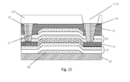
- the array substrate further includes: a flattening layer 111 located between the TFT and the pixel electrode 112 , the flattening layer 111 does not cover a third via hole 1111 (referring to FIG. 12 ) through which the drain electrode 110 is in contact with the pixel electrode 112 .
- a thickness of the top gate 17 is in the range of 150 nm-300 nm, and preferably is 200 nm; the active layer 14 is an ⁇ -Si film, and has a thickness in the range of 20 nm-100 nm.
- the first insulating layer 13 includes: SiO 2 and SiN x , wherein a part close to the bottom gate 12 uses SiN x , and a part close to the active layer 14 uses SiO 2 .
- the second insulating layer 16 includes: SiO 2 and SiN x , wherein a part close to the top gate 17 uses SiN x , and a part close to the active layer 14 uses SiO 2 .
- the array substrate of this embodiment has a structure substantially the same as that of the array substrate of Embodiment 1, and also includes: a base substrate 11 , a TFT, a gate line, a data line and a pixel electrode 112 formed on the base substrate 11 , the TFT includes: a bottom gate 12 , a first gate insulating layer 13 , an active layer 14 , a second gate insulating layer 16 , a top gate 17 , a gate isolation layer 18 and a source electrode 19 and a drain electrode 110 sequentially formed on the base substrate 11 , wherein the gate isolation layer 18 includes SiN x .
- the source electrode 19 and the drain electrode 110 are in contact with the active layer 14 through a first via hole 191 and a second via hole 1101 passing through the gate isolation layer 18 and the second insulating layer 16 , respectively; the pixel electrode 112 is in contact with the drain electrode 110 .
- the array substrate further includes: a flattening layer 111 located between the TFT and the pixel electrode 112 , the flattening layer 111 does not cover a third via hole 1111 (referring to FIG. 12 ) through which the drain electrode 110 is in contact with the pixel electrode 112 .
- a thickness of the top gate 17 is in the range of 150 nm-300 nm, and preferably is 200 nm; the active layer 14 is an ⁇ -Si film, and has a thickness in the range of 20 nm-100 nm.
- the first insulating layer 13 includes: SiO 2 and SiN x , wherein a part close to the bottom gate 12 uses SiN x , and a part close to the active layer 14 uses SiO 2 .
- the second insulating layer 16 includes: SiO 2 and SiN x , wherein a part close to the top gate 17 uses SiN x , and a part close to the active layer 14 uses SiO 2 .
- the TFT further includes a nickel layer 15 , the nickel layer 15 is disposed between the source electrode 19 and the active layer 14 , and a thickness of the nickel layer 15 is in the range of 20 nm-25 nm.
- the nickel layer 15 can induce lateral crystallization of the active layer (the ⁇ -Si film), which effectively reduces phase change energy of a crystallization process, the converted active layer is in a polycrystalline state, and high mobility of polysilicon helps to improve performance of a TFT device.
- the array substrate of this embodiment has a structure substantially the same as those of the array substrates of Embodiment 1 and Embodiment 2, and also includes: a base substrate 11 , a TFT, a gate line, a data line and a pixel electrode 112 formed on the base substrate 11 , the TFT includes: a bottom gate 12 , a first gate insulating layer 13 , an active layer 14 , a second gate insulating layer 16 , a top gate 17 , a gate isolation layer 18 and a source electrode 19 and a drain electrode 110 sequentially formed on the base substrate 11 , wherein the gate isolation layer 18 includes SiO 2 .
- the source electrode 19 and the drain electrode 110 are in contact with the active layer 14 through a first via hole 191 and a second via hole 1101 passing through the gate isolation layer 18 and the second insulating layer 16 , respectively; the pixel electrode 112 is in contact with the drain electrode 110 .
- the array substrate further includes: a flattening layer 111 located between the TFT and the pixel electrode 112 , the flattening layer 111 does not cover a third via hole 1111 (referring to FIG. 12 ) through which the drain electrode 110 is in contact with the pixel electrode 112 .
- a thickness of the top gate 17 is in the range of 150 nm-300 nm, and preferably is 200 nm; the active layer 14 is an ⁇ -Si film, and has a thickness in the range of 20 nm-100 nm.
- the first insulating layer 13 includes: SiO 2 and SiN x , wherein a part close to the bottom gate 12 uses SiN x , and a part close to the active layer 14 uses SiO 2 .
- the second insulating layer 16 includes: SiO 2 and SiN x , wherein a part close to the top gate 17 uses SiN x , and a part close to the active layer 14 uses SiO 2 .
- Embodiment 3 differs from the Embodiment 2 in that a nickel layer 15 included in the array substrate is disposed between the drain electrode 110 and the active layer 14 , or disposed between the source electrode 19 and the active layer 14 and between the drain electrode 110 and the active layer 14 ; a thickness of the nickel layer 15 is in the range of 20 nm-25 nm.
- the present invention also provides a method for fabricating an array substrate, which includes steps:
- S3′ as illustrated in FIG. 8 , doping the active layer 14 ; S3: as illustrated in FIGS. 9-12 and FIG. 1 , sequentially forming a gate isolation layer 18 , a source electrode 19 , a drain electrode 110 , a flattening layer 111 and a pixel electrode 112 illustrated in FIG. 1 on the top gate 17 .
- S3 specifically includes: forming an insulating film on the substrate formed by step of S3′, forming a first via hole 191 and a second via hole 1101 at an area where the source electrode 19 is to be formed and an area where the drain electrode 110 is to be formed, respectively, through a patterning process, and exposing the active layer 14 by the first via hole 191 and the second via hole 1101 ;
- a source-drain metal film forming patterns of the source electrode 19 and the drain electrode 110 through a patterning process, and forming a data line at the same time as forming the patterns of the source electrode 19 and the drain electrode 110 ;
- the flattening layer 111 formed between the TFT and the pixel electrode 112 does not cover the third via hole 1111 through which the drain electrode 110 is in contact with the pixel electrode 112 .
- Embodiment 4 As illustrated in FIGS. 4 to 12 , the method for fabricating an array substrate of this embodiment is substantially the same as that of Embodiment 4, which includes:
- S3 sequentially forming a gate isolation layer 18 , a source electrode 19 , a drain electrode 110 , a flattening layer 111 and a pixel electrode 112 illustrated in FIG. 1 on the top gate 17 .
- S3 specifically includes: forming an insulating film on the substrate formed by step of S3′, forming a first via hole 191 and a second via hole 1101 at an area where the source electrode 19 is to be formed and an area where the drain electrode 110 is to be formed, respectively, through a patterning process, and exposing the active layer 14 by the first via hole 191 and the second via hole 1101 ;
- a source-drain metal film forming patterns of the source electrode 19 and the drain electrode 110 through a patterning process, and forming a data line at the same time as forming the patterns of the source electrode 19 and the drain electrode 110 ;
- the flattening layer 111 formed between the TFT and the pixel electrode 112 does not cover the third via hole 1111 through which the drain electrode 110 is in contact with the pixel electrode 112 .
- Embodiment 5 differs from Embodiment 4 in that, as illustrated in FIG. 13 and referring to FIGS. 14 and 15 , this embodiment further includes S2′ before S2. and S2′ includes: forming a nickel layer 15 at an area on the active layer 14 where the source electrode 19 is to be formed, and then performing a heat treatment on the active layer 14 at a temperature of 500° C. for 2 hours in an atmosphere of H 2 .
- Adding metal Ni onto the active layer can effectively reduce energy of phase change converting from ⁇ -Si to P—Si, the converted active layer is in a polycrystalline state, and lateral crystallization can be achieved, and such a process is a metal-induced lateral crystallization process (MILC process).
- MILC process metal-induced lateral crystallization process
- a MILC process is employed, a nickel layer is deposited on the surface of an amorphous silicon film using a sputtering process, the amorphous silicon can be converted into polysilicon at a suitable temperature, and induced lateral crystallization is further achieved.
- This method effectively reduces energy of phase change in a crystallization process, and high mobility of polysilicon helps to improve performance of a device.
- the structure with two gates can make the carriers in sub-threshold state away from a Si—SiO 2 interface, which effectively reduces scattering of carriers in channel which results from the fact that they collide with too many defects when drifting under the source-drain electric field, and thus significantly improving mobility.
- the method for fabricating an array substrate of this embodiment is substantially the same as that of Embodiment 5, which also includes:
- S3 sequentially forming a gate isolation layer 18 , a source electrode 19 , a drain electrode 110 , a flattening layer 111 and a pixel electrode 112 illustrated in FIG. 1 on the top gate 17 .
- S3 specifically includes: forming an insulating film on the substrate formed in step S3′, forming a first via hole 191 and a second via hole 1101 at an area where the source electrode 19 is to be formed and an area where the drain electrode 110 is to be formed, respectively, through a patterning process, and exposing the active layer 14 by the first via hole 191 and the second via hole 1101 ;
- a source-drain metal film forming patterns of the source electrode 19 and the drain electrode 110 through a patterning process, and forming a data line at the same time as forming the patterns of the source electrode 19 and the drain electrode 110 ;
- the flattening layer 111 formed between the TFT and the pixel electrode 112 does not cover the third via hole 1111 through which the drain electrode 110 is in contact with the pixel electrode 112 .
- Embodiment 6 differs from Embodiment 5 in that this embodiment further includes S2′ before S2. and S2′ includes: forming a nickel layer 15 at an area on the active layer 14 where the drain electrode 110 is to be formed, and then performing a heat treatment on the active layer 14 at a temperature of 540° C. for 2 hours in an atmosphere of H 2 .
- Embodiment 6 The method for fabricating an array substrate of this embodiment is substantially the same as that of Embodiment 6, which also includes:
- S3 sequentially forming a gate isolation layer 18 , a source electrode 19 , a drain electrode 110 , a flattening layer 111 and a pixel electrode 112 illustrated in FIG. 1 on the top gate 17 .
- S3 specifically includes: forming an insulating film on the substrate formed in step S3′, forming a first via hole 191 and a second via hole 1101 at an area where the source electrode 19 is to be formed and an area where the drain electrode 110 is to be formed, respectively, through a patterning process, and exposing the active layer 14 by the first via hole 191 and the second via hole 1101 ;
- a source-drain metal film forming patterns of the source electrode 19 and the drain electrode 110 through a patterning process, and forming a data line at the same time as forming the patterns of the source electrode 19 and the drain electrode 110 ;
- the flattening layer 111 formed between the TFT and the pixel electrode 112 does not cover the third via hole 1111 through which the drain electrode 110 is in contact with the pixel electrode 112 .
- Embodiment 7 differs from Embodiments 6 and 5 in that this embodiment further includes S2′ before S2. and S2′ includes: forming a nickel layer 15 at an area on the active layer 14 where the source electrode 19 is to be formed and an area on the active layer 14 where the drain electrode 110 is to be formed, and then performing a heat treatment on the active layer 14 at a temperature of 570° C. for 2 hours in an atmosphere of H 2 .
- This embodiment provides a display device, which includes the array substrate described in any of the above embodiments.
Landscapes
- Physics & Mathematics (AREA)
- Nonlinear Science (AREA)
- Mathematical Physics (AREA)
- Engineering & Computer Science (AREA)
- Chemical & Material Sciences (AREA)
- Crystallography & Structural Chemistry (AREA)
- Microelectronics & Electronic Packaging (AREA)
- General Physics & Mathematics (AREA)
- Optics & Photonics (AREA)
- Thin Film Transistor (AREA)
- Liquid Crystal (AREA)
- Devices For Indicating Variable Information By Combining Individual Elements (AREA)
- Electroluminescent Light Sources (AREA)
Abstract
A method for fabricating an array substrate includes sequentially forming a bottom gate, a first gate insulating layer, an active layer and a second gate insulating layer on a base substrate, a gate line being formed at the same time as forming the bottom gate; forming a top gate on the second gate insulating layer; sequentially forming a gate isolation layer, a source electrode, a drain electrode and a pixel electrode on the top gate. Before forming the top gate on the second gate insulating layer, the method includes forming a nickel layer at an area on the active layer where the source electrode is to be formed and/or an area on the active layer where the drain electrode is to be formed, and then performing a heat treatment on the active layer at a temperature in the range of 500° C.-570° C. for 2 hours in an atmosphere of H2.
Description
This application is a division of U.S. patent application Ser. No. 14/089,841, now U.S. Pat. No. 9,214,482, filed Nov. 26, 2013, which claims the benefit of priority under 35 U.S.C. §119 of Chinese Patent Application Number 201210489122.2 filed Nov. 26, 2012, which is incorporated herein by reference in its entirety.
The present invention relates to the field of display technology, and particularly, to an array substrate and a method fabricating an array substrate, and a display device.
With the development of information and network, electronic display techniques have been widely used. Currently, liquid crystal display (LCD) display devices and active matrix/organic light emitting diode (AMOLED) display devices are popular. LCD and AMOLED display devices are generally driven using active matrix driving techniques, such as techniques for driving thin film transistor (TFT) array substrate.
Existing array substrates usually employ one-sided gate structure, an array substrate with one-sided gate structure has only a conductive channel existing at a side close to the gate when being turned on, and electrons are very likely to be scattered during their moving, which results in low mobility and limits performance of the array substrate.
Technical problems to be solved by the present invention are: providing an array substrate, a method for fabricating the array substrate, and a display device to improve performance of the array substrate, and improve driving ability and sub-threshold characteristics of the array substrate as well, directed to deficiencies in the prior art.
To solve the above problems, the present invention provides an array substrate, which includes: a base substrate; a TFT, a gate line, a data line and a pixel electrode formed on the base substrate, the TFT includes: a bottom gate, a first gate insulating layer, an active layer, a second gate insulating layer, a top gate, a gate isolation layer and a source electrode and a drain electrode sequentially formed on the base substrate; wherein, the source electrode and the drain electrode are in contact with the active layer through a first via hole and a second via hole passing through the gate isolation layer and the second insulating layer, respectively; the pixel electrode is in contact with the drain electrode.
Wherein, the array substrate further includes: a flattening layer located between the TFT and the pixel electrode, the flattening layer does not cover a third via hole through which the drain electrode is in contact with the pixel electrode.
Wherein, the array substrate further includes a nickel layer, the nickel layer is disposed between the source electrode and the active layer and/or between the drain electrode and the active layer.
Wherein, a thickness of the top gate is in the range of 150 nm-300 nm.
Preferably, the thickness of the top gate is 200 nm.
Wherein, a thickness of the nickel layer is in the range of 20 nm-25 nm.
Wherein, a thickness of the active layer is in the range of 20 nm-100 nm.
Wherein, material of the gate isolation layer includes SiO2 and/or SiNx.
The present invention further provides a display device, characterized in that it includes the above array substrate.
The present invention further provides a method for fabricating an array substrate, which includes steps:
S1: sequentially forming a bottom gate, a first gate insulating layer, an active layer and a second gate insulating layer on a base substrate, wherein a gate line is formed at the same time as forming the bottom gate;
S2: forming a top gate on the second gate insulating layer;
S3: sequentially forming a gate isolation layer, a source electrode, a drain electrode and a pixel electrode on the top gate.
Wherein, before step S2, the method further includes step S2′ including: forming a nickel layer at an area on the active layer where the source electrode is to be formed and/or an area on the active layer where the drain electrode is to be formed, and then performing a heat treatment on the active layer at a temperature in the range of 500° C.-570° C. for 2 hours in an atmosphere of H2.
Wherein, before step S3, the method further includes step S3′ including: doping the active layer subjected to the heat treatment in step S2′.
Wherein, step S3 includes: forming an insulating film on the substrate formed in step S3′, forming a first via hole and a second via hole at an area where the source electrode is to be formed and an area where the drain electrode is to be formed, respectively, through a patterning process, and exposing the active layer by the first via hole and the second via hole;
forming a source-drain metal film, forming patterns of the source electrode and the drain electrode through a patterning process, and forming a data line at the same time as forming the patterns of the source electrode and the drain electrode;
forming a flattening layer film, forming a third via hole at an area corresponding to the drain electrode in the flattening layer film through a patterning process, so as to form a pattern of the flattening layer; and
forming a transparent conductive film, and forming a pattern of the pixel electrode through a patterning process, the pixel electrode being in contact with the drain electrode;
wherein, the flattening layer formed between the TFT and the pixel electrode does not cover the third via hole through which the drain electrode is in contact with the pixel electrode.
The array substrate provided by the present invention employs a two-sided gate structure, that is, gates are formed at both sides of the active layer, an array substrate with the two-sided gate structure has conductive channels existing at both sides of the active layer when being turned on, carriers are not likely to be scattered during their moving, forming inversion layers at both upper and lower surfaces at the same time can be achieved in a situation where a proper silicon film (active layer) is selected, carrier concentrations in the inversion layers at both upper and lower surfaces increase rapidly with increase of gate voltage in a situation where the silicon film is fully depleted, and driving ability, and sub-threshold and frequency response characteristics of the array substrate are closer to an ideal state.
Wherein, 11: substrate; 12: bottom gate; 13: first gate insulating layer; 14: active layer; 15: nickel layer; 16: second gate insulating layer; 17: top gate; 18: gate isolation layer; 19: source electrode; 110: drain electrode; 111: flattening layer; 112: pixel electrode; 191: first via hole; 1101: second via hole; 1111: third via hole.
Specific implementations of the present invention will be further described below in details with reference to the drawings and the embodiments. The below embodiments are used to explain the present invention, but not used to limit the scope the present invention.
As illustrated in FIG. 1 , the present invention provides an array substrate, which includes: a base substrate 11, a TFT, a gate line, a data line and a pixel electrode 112 formed on the base substrate 11, the TFT includes: a bottom gate 12, a first gate insulating layer 13, an active layer 14, a second gate insulating layer 16, a top gate 17, a gate isolation layer 18 and a source electrode 19 and a drain electrode 110 sequentially formed on the base substrate 11, wherein material of the gate isolation layer 18 includes SiO2 and/or SiNx.
In this embodiment, forming inversion layers at both upper and lower surfaces of a silicon film at the same time can be achieved in a situation where a proper silicon film is selected, carrier concentrations in the inversion layers of both upper and lower surfaces increase rapidly with the increase of gate voltage in a situation where the silicon film is fully depleted, and the driving ability and sub-threshold and frequency response characteristics of the array substrate are closer to an ideal state.
Wherein, the source electrode 19 and the drain electrode 110 are in contact with the active layer 14 through a first via hole 191 and a second via hole 1101 passing through the gate isolation layer 18 and the second insulating layer 16 (referring to FIG. 10 ), respectively; the pixel electrode 112 is in contact with the drain electrode 110.
The array substrate further includes: a flattening layer 111 located between the TFT and the pixel electrode 112, the flattening layer 111 does not cover a third via hole 1111 (referring to FIG. 12 ) through which the drain electrode 110 is in contact with the pixel electrode 112.
A thickness of the top gate 17 is in the range of 150 nm-300 nm, and preferably is 200 nm; the active layer 14 is an α-Si film, and has a thickness in the range of 20 nm-100 nm.
The first insulating layer 13 includes: SiO2 and SiNx, wherein a part close to the bottom gate 12 uses SiNx, and a part close to the active layer 14 uses SiO2.
The second insulating layer 16 includes: SiO2 and SiNx, wherein a part close to the top gate 17 uses SiNx, and a part close to the active layer 14 uses SiO2.
As illustrated in FIG. 2 , the array substrate of this embodiment has a structure substantially the same as that of the array substrate of Embodiment 1, and also includes: a base substrate 11, a TFT, a gate line, a data line and a pixel electrode 112 formed on the base substrate 11, the TFT includes: a bottom gate 12, a first gate insulating layer 13, an active layer 14, a second gate insulating layer 16, a top gate 17, a gate isolation layer 18 and a source electrode 19 and a drain electrode 110 sequentially formed on the base substrate 11, wherein the gate isolation layer 18 includes SiNx.
Wherein, the source electrode 19 and the drain electrode 110 are in contact with the active layer 14 through a first via hole 191 and a second via hole 1101 passing through the gate isolation layer 18 and the second insulating layer 16, respectively; the pixel electrode 112 is in contact with the drain electrode 110.
The array substrate further includes: a flattening layer 111 located between the TFT and the pixel electrode 112, the flattening layer 111 does not cover a third via hole 1111 (referring to FIG. 12 ) through which the drain electrode 110 is in contact with the pixel electrode 112.
A thickness of the top gate 17 is in the range of 150 nm-300 nm, and preferably is 200 nm; the active layer 14 is an α-Si film, and has a thickness in the range of 20 nm-100 nm.
The first insulating layer 13 includes: SiO2 and SiNx, wherein a part close to the bottom gate 12 uses SiNx, and a part close to the active layer 14 uses SiO2.
The second insulating layer 16 includes: SiO2 and SiNx, wherein a part close to the top gate 17 uses SiNx, and a part close to the active layer 14 uses SiO2.
The difference between the array substrates of the above two embodiment exists in that the TFT further includes a nickel layer 15, the nickel layer 15 is disposed between the source electrode 19 and the active layer 14, and a thickness of the nickel layer 15 is in the range of 20 nm-25 nm.
The nickel layer 15 can induce lateral crystallization of the active layer (the α-Si film), which effectively reduces phase change energy of a crystallization process, the converted active layer is in a polycrystalline state, and high mobility of polysilicon helps to improve performance of a TFT device.
The array substrate of this embodiment has a structure substantially the same as those of the array substrates of Embodiment 1 and Embodiment 2, and also includes: a base substrate 11, a TFT, a gate line, a data line and a pixel electrode 112 formed on the base substrate 11, the TFT includes: a bottom gate 12, a first gate insulating layer 13, an active layer 14, a second gate insulating layer 16, a top gate 17, a gate isolation layer 18 and a source electrode 19 and a drain electrode 110 sequentially formed on the base substrate 11, wherein the gate isolation layer 18 includes SiO2.
Wherein, the source electrode 19 and the drain electrode 110 are in contact with the active layer 14 through a first via hole 191 and a second via hole 1101 passing through the gate isolation layer 18 and the second insulating layer 16, respectively; the pixel electrode 112 is in contact with the drain electrode 110.
The array substrate further includes: a flattening layer 111 located between the TFT and the pixel electrode 112, the flattening layer 111 does not cover a third via hole 1111 (referring to FIG. 12 ) through which the drain electrode 110 is in contact with the pixel electrode 112.
A thickness of the top gate 17 is in the range of 150 nm-300 nm, and preferably is 200 nm; the active layer 14 is an α-Si film, and has a thickness in the range of 20 nm-100 nm.
The first insulating layer 13 includes: SiO2 and SiNx, wherein a part close to the bottom gate 12 uses SiNx, and a part close to the active layer 14 uses SiO2.
The second insulating layer 16 includes: SiO2 and SiNx, wherein a part close to the top gate 17 uses SiNx, and a part close to the active layer 14 uses SiO2.
As illustrated in FIG. 3 and referring to FIGS. 4 to 12 , the present invention also provides a method for fabricating an array substrate, which includes steps:
S1: as illustrated in FIGS. 4 to 6 , sequentially forming a bottom gate 12, a first gate insulating layer 13, an active layer 14 and a second gate insulating layer 16 on a base substrate 11, wherein a gate line is formed at the same time as forming the bottom gate 12;
S2: as illustrated in FIG. 7 , forming a top gate 17 on the second gate insulating layer 16;
S3′: as illustrated in FIG. 8 , doping the active layer 14; S3: as illustrated in FIGS. 9-12 and FIG. 1 , sequentially forming a gate isolation layer 18, a source electrode 19, a drain electrode 110, a flattening layer 111 and a pixel electrode 112 illustrated in FIG. 1 on the top gate 17.
S3 specifically includes: forming an insulating film on the substrate formed by step of S3′, forming a first via hole 191 and a second via hole 1101 at an area where the source electrode 19 is to be formed and an area where the drain electrode 110 is to be formed, respectively, through a patterning process, and exposing the active layer 14 by the first via hole 191 and the second via hole 1101;
forming a source-drain metal film, forming patterns of the source electrode 19 and the drain electrode 110 through a patterning process, and forming a data line at the same time as forming the patterns of the source electrode 19 and the drain electrode 110;
forming a flattening layer film, forming a third via hole 1111 at an area corresponding to the drain electrode 110 in the flattening layer film through a patterning process, so as to form a pattern of the flattening layer 111 (referring to FIG. 12 ); and
forming a transparent conductive film, forming a pattern of the pixel electrode 112 through a patterning process, and the pixel electrode 112 is in contact with the drain electrode 110.
Wherein, the flattening layer 111 formed between the TFT and the pixel electrode 112 does not cover the third via hole 1111 through which the drain electrode 110 is in contact with the pixel electrode 112.
As illustrated in FIGS. 4 to 12 , the method for fabricating an array substrate of this embodiment is substantially the same as that of Embodiment 4, which includes:
S1: sequentially forming a bottom gate 12, a first gate insulating layer 13, an active layer 14 and a second gate insulating layer 16 on a base substrate 11, wherein a gate line is formed at the same time as forming the bottom gate 12;
S2: forming a top gate 17 on the second gate insulating layer 16;
S3′: doping the active layer 14;
S3: sequentially forming a gate isolation layer 18, a source electrode 19, a drain electrode 110, a flattening layer 111 and a pixel electrode 112 illustrated in FIG. 1 on the top gate 17.
S3 specifically includes: forming an insulating film on the substrate formed by step of S3′, forming a first via hole 191 and a second via hole 1101 at an area where the source electrode 19 is to be formed and an area where the drain electrode 110 is to be formed, respectively, through a patterning process, and exposing the active layer 14 by the first via hole 191 and the second via hole 1101;
forming a source-drain metal film, forming patterns of the source electrode 19 and the drain electrode 110 through a patterning process, and forming a data line at the same time as forming the patterns of the source electrode 19 and the drain electrode 110;
forming a flattening layer film, forming a third via hole 1111 at an area corresponding to the drain electrode 110 in the flattening layer film through a patterning process, so as to form a pattern of the flattening layer 111 (referring to FIG. 12 ); and
forming a transparent conductive film, forming a pattern of the pixel electrode 112 through a patterning process, and the pixel electrode 112 is in contact with the drain electrode 110.
Wherein, the flattening layer 111 formed between the TFT and the pixel electrode 112 does not cover the third via hole 1111 through which the drain electrode 110 is in contact with the pixel electrode 112.
Embodiment 5 differs from Embodiment 4 in that, as illustrated in FIG. 13 and referring to FIGS. 14 and 15 , this embodiment further includes S2′ before S2. and S2′ includes: forming a nickel layer 15 at an area on the active layer 14 where the source electrode 19 is to be formed, and then performing a heat treatment on the active layer 14 at a temperature of 500° C. for 2 hours in an atmosphere of H2.
Adding metal Ni onto the active layer (the α-Si film) can effectively reduce energy of phase change converting from α-Si to P—Si, the converted active layer is in a polycrystalline state, and lateral crystallization can be achieved, and such a process is a metal-induced lateral crystallization process (MILC process).
In this embodiment, a MILC process is employed, a nickel layer is deposited on the surface of an amorphous silicon film using a sputtering process, the amorphous silicon can be converted into polysilicon at a suitable temperature, and induced lateral crystallization is further achieved. This method effectively reduces energy of phase change in a crystallization process, and high mobility of polysilicon helps to improve performance of a device. The structure with two gates can make the carriers in sub-threshold state away from a Si—SiO2 interface, which effectively reduces scattering of carriers in channel which results from the fact that they collide with too many defects when drifting under the source-drain electric field, and thus significantly improving mobility.
The method for fabricating an array substrate of this embodiment is substantially the same as that of Embodiment 5, which also includes:
S1: sequentially forming a bottom gate 12, a first gate insulating layer 13, an active layer 14 and a second gate insulating layer 16 on a base substrate 11, wherein a gate line is formed at the same time as forming the bottom gate 12;
S2: forming a top gate 17 on the second gate insulating layer 16;
S3′: doping the active layer 14;
S3: sequentially forming a gate isolation layer 18, a source electrode 19, a drain electrode 110, a flattening layer 111 and a pixel electrode 112 illustrated in FIG. 1 on the top gate 17.
S3 specifically includes: forming an insulating film on the substrate formed in step S3′, forming a first via hole 191 and a second via hole 1101 at an area where the source electrode 19 is to be formed and an area where the drain electrode 110 is to be formed, respectively, through a patterning process, and exposing the active layer 14 by the first via hole 191 and the second via hole 1101;
forming a source-drain metal film, forming patterns of the source electrode 19 and the drain electrode 110 through a patterning process, and forming a data line at the same time as forming the patterns of the source electrode 19 and the drain electrode 110;
forming a flattening layer film, forming a third via hole 1111 at an area corresponding to the drain electrode 110 in the flattening layer film through a patterning process, so as to form a pattern of the flattening layer 111 (referring to FIG. 12 ); and
forming a transparent conductive film, forming a pattern of the pixel electrode 112 through a patterning process, and the pixel electrode 112 is in contact with the drain electrode 110.
Wherein, the flattening layer 111 formed between the TFT and the pixel electrode 112 does not cover the third via hole 1111 through which the drain electrode 110 is in contact with the pixel electrode 112.
Embodiment 6 differs from Embodiment 5 in that this embodiment further includes S2′ before S2. and S2′ includes: forming a nickel layer 15 at an area on the active layer 14 where the drain electrode 110 is to be formed, and then performing a heat treatment on the active layer 14 at a temperature of 540° C. for 2 hours in an atmosphere of H2.
The method for fabricating an array substrate of this embodiment is substantially the same as that of Embodiment 6, which also includes:
S1: sequentially forming a bottom gate 12, a first gate insulating layer 13, an active layer 14 and a second gate insulating layer 16 on a base substrate 11, wherein a gate line is formed at the same time as forming the bottom gate 12;
S2: forming a top gate 17 on the second gate insulating layer 16;
S3′: doping the active layer 14;
S3: sequentially forming a gate isolation layer 18, a source electrode 19, a drain electrode 110, a flattening layer 111 and a pixel electrode 112 illustrated in FIG. 1 on the top gate 17.
S3 specifically includes: forming an insulating film on the substrate formed in step S3′, forming a first via hole 191 and a second via hole 1101 at an area where the source electrode 19 is to be formed and an area where the drain electrode 110 is to be formed, respectively, through a patterning process, and exposing the active layer 14 by the first via hole 191 and the second via hole 1101;
forming a source-drain metal film, forming patterns of the source electrode 19 and the drain electrode 110 through a patterning process, and forming a data line at the same time as forming the patterns of the source electrode 19 and the drain electrode 110;
forming a flattening layer film, forming a third via hole 1111 at an area corresponding to the drain electrode 110 in the flattening layer film through a patterning process, so as to form a pattern of the flattening layer 111 (referring to FIG. 12 ); and
forming a transparent conductive film, forming a pattern of the pixel electrode 112 through a patterning process, and the pixel electrode 112 is in contact with the drain electrode 110.
Wherein, the flattening layer 111 formed between the TFT and the pixel electrode 112 does not cover the third via hole 1111 through which the drain electrode 110 is in contact with the pixel electrode 112.
Embodiment 7 differs from Embodiments 6 and 5 in that this embodiment further includes S2′ before S2. and S2′ includes: forming a nickel layer 15 at an area on the active layer 14 where the source electrode 19 is to be formed and an area on the active layer 14 where the drain electrode 110 is to be formed, and then performing a heat treatment on the active layer 14 at a temperature of 570° C. for 2 hours in an atmosphere of H2.
This embodiment provides a display device, which includes the array substrate described in any of the above embodiments.
The above implementations are only used to explain the present invention, but not to limit the present invention, the person skilled in the art can make various variations and modifications without departing from the spirit and scope of the present invention, therefore, all equivalent technical solutions fall within the scope of the present invention, and the protection scope of the present invention should be defined by the claims.
Claims (3)
1. A method for fabricating an array substrate, including steps:
S1: sequentially forming a bottom gate, a first gate insulating layer, an active layer and a second gate insulating layer on a base substrate, wherein a gate line is formed at the same time as forming the bottom gate;
S2: forming a top gate on the second gate insulating layer;
S3: sequentially forming a gate isolation layer, a source electrode, a drain electrode and a pixel electrode on the top gate;
wherein the method further includes step S2′ before step S2, and step S2′ includes:
forming a nickel layer at an area on the active layer where the source electrode is to be formed and/or an area on the active layer where the drain electrode is to be formed, and then performing a heat treatment on the active layer at a temperature in the range of 500° C.-570° C. for 2 hours in an atmosphere of H2.
2. The method for fabricating an array substrate of claim 1 , further including step S3′ before step S3, and step S3′ including doping the active layer subjected to the heat treatment in step S2′.
3. The method for fabricating an array substrate of claim 2 , wherein step S3 includes:
forming an insulating film on the substrate formed in step S3′, forming a first via hole and a second via hole at an area where the source electrode is to be formed and an area where the drain electrode is to be formed, respectively, through a patterning process, and exposing the active layer by the first via hole and the second via hole;
forming a source-drain metal film, forming patterns of the source electrode and the drain electrode through a patterning process, and forming a data line at the same time as forming the patterns of the source electrode and the drain electrode;
forming a flattening layer film, forming a third via hole at an area corresponding to the drain electrode in the flattening layer film through a patterning process, so as to form a pattern of the flattening layer; and
forming a transparent conductive film, and forming pattern of the pixel electrode through a patterning process, the pixel electrode being in contact with the drain electrode;
wherein, the flattening layer formed between the TFT and the pixel electrode does not cover the third via hole through which the drain electrode is in contact with the pixel electrode.
Priority Applications (1)
| Application Number | Priority Date | Filing Date | Title |
|---|---|---|---|
| US14/934,864 US9502448B2 (en) | 2012-11-26 | 2015-11-06 | Method for fabricating an array substrate with improved driving ability |
Applications Claiming Priority (5)
| Application Number | Priority Date | Filing Date | Title |
|---|---|---|---|
| CN2012104891222A CN102956649A (en) | 2012-11-26 | 2012-11-26 | Array baseplate, manufacturing method of array baseplate and display device |
| CN201210489122 | 2012-11-26 | ||
| CN201210489122.2 | 2012-11-26 | ||
| US14/089,841 US9214482B2 (en) | 2012-11-26 | 2013-11-26 | Array substrate and display device |
| US14/934,864 US9502448B2 (en) | 2012-11-26 | 2015-11-06 | Method for fabricating an array substrate with improved driving ability |
Related Parent Applications (1)
| Application Number | Title | Priority Date | Filing Date |
|---|---|---|---|
| US14/089,841 Division US9214482B2 (en) | 2012-11-26 | 2013-11-26 | Array substrate and display device |
Publications (2)
| Publication Number | Publication Date |
|---|---|
| US20160064418A1 US20160064418A1 (en) | 2016-03-03 |
| US9502448B2 true US9502448B2 (en) | 2016-11-22 |
Family
ID=47765228
Family Applications (2)
| Application Number | Title | Priority Date | Filing Date |
|---|---|---|---|
| US14/089,841 Expired - Fee Related US9214482B2 (en) | 2012-11-26 | 2013-11-26 | Array substrate and display device |
| US14/934,864 Active US9502448B2 (en) | 2012-11-26 | 2015-11-06 | Method for fabricating an array substrate with improved driving ability |
Family Applications Before (1)
| Application Number | Title | Priority Date | Filing Date |
|---|---|---|---|
| US14/089,841 Expired - Fee Related US9214482B2 (en) | 2012-11-26 | 2013-11-26 | Array substrate and display device |
Country Status (5)
| Country | Link |
|---|---|
| US (2) | US9214482B2 (en) |
| EP (1) | EP2736077B1 (en) |
| JP (1) | JP2014106539A (en) |
| KR (1) | KR20140067926A (en) |
| CN (1) | CN102956649A (en) |
Cited By (1)
| Publication number | Priority date | Publication date | Assignee | Title |
|---|---|---|---|---|
| US10593807B2 (en) * | 2017-12-26 | 2020-03-17 | Shenzhen China Star Optoelectronics Semiconductor Display Technology Co., Ltd. | Array substrate and fabricating method thereof |
Families Citing this family (23)
| Publication number | Priority date | Publication date | Assignee | Title |
|---|---|---|---|---|
| US8673426B2 (en) * | 2011-06-29 | 2014-03-18 | Semiconductor Energy Laboratory Co., Ltd. | Driver circuit, method of manufacturing the driver circuit, and display device including the driver circuit |
| US9419568B2 (en) | 2013-06-03 | 2016-08-16 | Skyworks Solutions, Inc. | Circuits and methods related to power amplifier efficiency based on multi-harmonic approximation |
| US9818765B2 (en) | 2013-08-26 | 2017-11-14 | Apple Inc. | Displays with silicon and semiconducting oxide thin-film transistors |
| CN103715267A (en) * | 2013-12-30 | 2014-04-09 | 京东方科技集团股份有限公司 | TFT, TFT array substrate, manufacturing method of TFT array substrate and display device |
| US9722090B2 (en) * | 2014-06-23 | 2017-08-01 | Semiconductor Energy Laboratory Co., Ltd. | Semiconductor device including first gate oxide semiconductor film, and second gate |
| CN104183607A (en) * | 2014-08-14 | 2014-12-03 | 深圳市华星光电技术有限公司 | Array substrate, manufacturing method of array substrate and display device with array substrate |
| US9543370B2 (en) * | 2014-09-24 | 2017-01-10 | Apple Inc. | Silicon and semiconducting oxide thin-film transistor displays |
| CN204314580U (en) * | 2015-01-08 | 2015-05-06 | 京东方科技集团股份有限公司 | A kind of dot structure, array base palte, display panel and display device |
| CN104867870B (en) * | 2015-04-14 | 2017-09-01 | 深圳市华星光电技术有限公司 | The preparation method and its structure of dual gate oxide semiconductor TFT substrate |
| CN104900653B (en) * | 2015-04-14 | 2017-12-29 | 深圳市华星光电技术有限公司 | TFT layout structure |
| CN104779203B (en) * | 2015-04-23 | 2017-11-28 | 京东方科技集团股份有限公司 | A kind of array base palte and its manufacture method, display device |
| CN105097941B (en) * | 2015-05-28 | 2019-02-26 | 京东方科技集团股份有限公司 | A thin film transistor and its manufacturing method, an array substrate, and a display device |
| JP6920785B2 (en) * | 2015-08-19 | 2021-08-18 | 株式会社ジャパンディスプレイ | Display device |
| US9818344B2 (en) | 2015-12-04 | 2017-11-14 | Apple Inc. | Display with light-emitting diodes |
| CN106483726B (en) * | 2016-12-21 | 2023-07-25 | 昆山龙腾光电股份有限公司 | Thin film transistor array substrate and manufacturing method, and liquid crystal display panel |
| CN106876330A (en) * | 2017-02-28 | 2017-06-20 | 上海中航光电子有限公司 | A kind of array base palte and preparation method thereof, display panel and display device |
| CN106920836A (en) * | 2017-03-29 | 2017-07-04 | 京东方科技集团股份有限公司 | A kind of thin film transistor (TFT) and preparation method thereof, array base palte, display device |
| CN107393933B (en) * | 2017-07-31 | 2020-08-04 | 京东方科技集团股份有限公司 | Manufacturing method of array substrate, array substrate and display panel |
| CN108122932B (en) * | 2017-12-26 | 2020-06-05 | 深圳市华星光电半导体显示技术有限公司 | Array substrate and preparation method thereof |
| CN108767016B (en) * | 2018-05-21 | 2021-09-21 | 京东方科技集团股份有限公司 | Thin film transistor, manufacturing method thereof, array substrate and display device |
| CN109378409B (en) * | 2018-10-18 | 2020-04-14 | 纳晶科技股份有限公司 | Electroluminescent device and manufacturing method thereof |
| CN110349975A (en) * | 2019-07-03 | 2019-10-18 | 深圳市华星光电半导体显示技术有限公司 | A kind of display panel and preparation method thereof |
| CN110634843B (en) * | 2019-08-27 | 2021-08-24 | 武汉华星光电半导体显示技术有限公司 | Thin film transistor, method for making the same, and display panel |
Citations (10)
| Publication number | Priority date | Publication date | Assignee | Title |
|---|---|---|---|---|
| US5834797A (en) | 1995-11-21 | 1998-11-10 | Sony Corporation | Transistor having first and second gate electrodes |
| US6015724A (en) | 1995-11-02 | 2000-01-18 | Semiconductor Energy Laboratory Co. | Manufacturing method of a semiconductor device |
| US20010030323A1 (en) | 2000-03-29 | 2001-10-18 | Sony Corporation | Thin film semiconductor apparatus and method for driving the same |
| US20020034842A1 (en) | 2000-09-15 | 2002-03-21 | Joo Seung Ki | Poly-silicon thin film transistor having back bias effects and fabrication method thereof |
| US20020139979A1 (en) | 2001-03-30 | 2002-10-03 | Joo Seung Ki | Method of crystallizing a silicon layer and method of fabricating a semiconductor device using the same |
| US6534788B1 (en) | 1998-07-30 | 2003-03-18 | Lg Philips Lcd Co., Ltd | Thin film transistor having dual gate structure and a fabricating method thereof |
| US20070026555A1 (en) | 2005-04-11 | 2007-02-01 | Lg Philips Lcd Co., Ltd. | Method of fabricating array substrate for liquid crystal display device |
| KR20070081218A (en) | 2006-02-10 | 2007-08-16 | 황진하 | A method of forming a nickel oxide thin film, a method of crystallizing an amorphous silicon thin film using the same, and a method of manufacturing a thin film transistor. |
| US20110024755A1 (en) | 2009-07-29 | 2011-02-03 | Nec Lcd Technologies, Ltd. | Thin film transistor substrate and thin film transistor used for the same |
| CN102709184A (en) | 2011-05-13 | 2012-10-03 | 京东方科技集团股份有限公司 | Polysilicon active layer-containing thin film transistor, manufacturing method thereof and array substrate |
Family Cites Families (10)
| Publication number | Priority date | Publication date | Assignee | Title |
|---|---|---|---|---|
| JPH04302475A (en) * | 1991-03-29 | 1992-10-26 | Kyocera Corp | Thin-film transistor |
| JP3067949B2 (en) * | 1994-06-15 | 2000-07-24 | シャープ株式会社 | Electronic device and liquid crystal display device |
| JPH09186101A (en) * | 1995-11-02 | 1997-07-15 | Semiconductor Energy Lab Co Ltd | Semiconductor device manufacturing method |
| JP4086925B2 (en) * | 1996-12-27 | 2008-05-14 | 株式会社半導体エネルギー研究所 | Active matrix display |
| JP3765902B2 (en) * | 1997-02-19 | 2006-04-12 | 株式会社半導体エネルギー研究所 | Manufacturing method of semiconductor device and manufacturing method of electronic device |
| US5940693A (en) * | 1997-07-15 | 1999-08-17 | Sharp Laboratories Of America, Inc. | Selective silicide thin-film transistor and method for same |
| US6278130B1 (en) * | 1998-05-08 | 2001-08-21 | Seung-Ki Joo | Liquid crystal display and fabricating method thereof |
| JP4008133B2 (en) * | 1998-12-25 | 2007-11-14 | 株式会社半導体エネルギー研究所 | Semiconductor device |
| JP2003115593A (en) * | 2001-10-04 | 2003-04-18 | Seiko Epson Corp | Electro-optical device and method for manufacturing the same, electronic apparatus, and thin film transistor |
| KR100611744B1 (en) * | 2003-11-22 | 2006-08-10 | 삼성에스디아이 주식회사 | Thin film transistor using metal induced lateral crystallization and its manufacturing method |
-
2012
- 2012-11-26 CN CN2012104891222A patent/CN102956649A/en active Pending
-
2013
- 2013-11-20 EP EP13193660.1A patent/EP2736077B1/en not_active Not-in-force
- 2013-11-25 JP JP2013242650A patent/JP2014106539A/en active Pending
- 2013-11-25 KR KR1020130144114A patent/KR20140067926A/en not_active Ceased
- 2013-11-26 US US14/089,841 patent/US9214482B2/en not_active Expired - Fee Related
-
2015
- 2015-11-06 US US14/934,864 patent/US9502448B2/en active Active
Patent Citations (12)
| Publication number | Priority date | Publication date | Assignee | Title |
|---|---|---|---|---|
| US6015724A (en) | 1995-11-02 | 2000-01-18 | Semiconductor Energy Laboratory Co. | Manufacturing method of a semiconductor device |
| US5834797A (en) | 1995-11-21 | 1998-11-10 | Sony Corporation | Transistor having first and second gate electrodes |
| US6534788B1 (en) | 1998-07-30 | 2003-03-18 | Lg Philips Lcd Co., Ltd | Thin film transistor having dual gate structure and a fabricating method thereof |
| US20010030323A1 (en) | 2000-03-29 | 2001-10-18 | Sony Corporation | Thin film semiconductor apparatus and method for driving the same |
| KR20010093719A (en) | 2000-03-29 | 2001-10-29 | 이데이 노부유끼 | Thin film semiconductor device and the driving method |
| US20020034842A1 (en) | 2000-09-15 | 2002-03-21 | Joo Seung Ki | Poly-silicon thin film transistor having back bias effects and fabrication method thereof |
| US20020139979A1 (en) | 2001-03-30 | 2002-10-03 | Joo Seung Ki | Method of crystallizing a silicon layer and method of fabricating a semiconductor device using the same |
| US20070026555A1 (en) | 2005-04-11 | 2007-02-01 | Lg Philips Lcd Co., Ltd. | Method of fabricating array substrate for liquid crystal display device |
| KR20070081218A (en) | 2006-02-10 | 2007-08-16 | 황진하 | A method of forming a nickel oxide thin film, a method of crystallizing an amorphous silicon thin film using the same, and a method of manufacturing a thin film transistor. |
| US20110024755A1 (en) | 2009-07-29 | 2011-02-03 | Nec Lcd Technologies, Ltd. | Thin film transistor substrate and thin film transistor used for the same |
| CN102709184A (en) | 2011-05-13 | 2012-10-03 | 京东方科技集团股份有限公司 | Polysilicon active layer-containing thin film transistor, manufacturing method thereof and array substrate |
| US20120289007A1 (en) | 2011-05-13 | 2012-11-15 | Boe Technology Group Co., Ltd. | Manufacturing method for thin film transistor with polysilicon active layer |
Non-Patent Citations (4)
| Title |
|---|
| European search report issued by European Patent Office for corresponding application 13193660 dated Feb. 10, 2014. |
| First office action issued by Chinese Patent Office for priority application 201210489122.2 dated Aug. 29, 2014 with English translation. |
| Notice of Preliminary Rejection issued by Korean Intellectual Property Office for corresponding application 10-2013-0144114 dated Dec. 1, 2014 with English translation. |
| Second office action issued by Chinese Patent Office for priority application 201210489122.2 dated Dec. 16, 2014 with English translation. |
Cited By (1)
| Publication number | Priority date | Publication date | Assignee | Title |
|---|---|---|---|---|
| US10593807B2 (en) * | 2017-12-26 | 2020-03-17 | Shenzhen China Star Optoelectronics Semiconductor Display Technology Co., Ltd. | Array substrate and fabricating method thereof |
Also Published As
| Publication number | Publication date |
|---|---|
| CN102956649A (en) | 2013-03-06 |
| EP2736077A1 (en) | 2014-05-28 |
| KR20140067926A (en) | 2014-06-05 |
| EP2736077B1 (en) | 2022-07-06 |
| JP2014106539A (en) | 2014-06-09 |
| US20160064418A1 (en) | 2016-03-03 |
| US9214482B2 (en) | 2015-12-15 |
| US20140145199A1 (en) | 2014-05-29 |
Similar Documents
| Publication | Publication Date | Title |
|---|---|---|
| US9502448B2 (en) | Method for fabricating an array substrate with improved driving ability | |
| CN106057735B (en) | TFT backplane manufacturing method and TFT backplane | |
| CN204391121U (en) | A kind of display unit, array base palte and thin-film transistor | |
| CN105390451B (en) | The preparation method of low temperature polycrystalline silicon TFT substrate | |
| CN103489920B (en) | A kind of thin film transistor (TFT) and preparation method thereof, array base palte and display device | |
| CN106098628B (en) | The production method and TFT backplate of TFT backplate | |
| US8119465B1 (en) | Thin film transistor and method for fabricating the same | |
| CN107425044B (en) | A flexible display panel, its manufacturing method and display device | |
| US9368634B2 (en) | Display panel, thin film transistor and method of fabricating the same | |
| CN104362179B (en) | Thin-film transistor, manufacturing method of thin-film transistor, array substrate and display device | |
| CN104576750A (en) | Thin-film transistor structure | |
| CN102751200B (en) | Thin film transistor, array substrateand manufacturing method thereof | |
| CN103762244A (en) | Thin film transistor, manufacturing method of thin film transistor, thin film transistor array substrate and liquid crystal panel | |
| CN102064109A (en) | Thin film transistor and method of manufacturing the same | |
| CN107170784A (en) | A kind of OLED array and preparation method thereof and OLED display | |
| WO2016201725A1 (en) | Method for manufacturing low-temperature polysilicon thin film transistor (tft) substrate and low-temperature polysilicon tft substrate | |
| WO2016090807A1 (en) | Array substrate, manufacturing method therefor, and display device | |
| CN102709283A (en) | Low temperature polysilicon thin film transistor (LTPS TFT) array substrate and manufacturing method thereof | |
| US10192903B2 (en) | Method for manufacturing TFT substrate | |
| WO2020062426A1 (en) | Array substrate and preparation method therefor, and display device | |
| CN104505404A (en) | Thin film transistor, preparation method of thin film transistor, array substrate adopting thin film transistor and display device adopting thin film transistor | |
| US10629746B2 (en) | Array substrate and manufacturing method thereof | |
| CN105990448B (en) | thin film transistor | |
| CN105870195B (en) | Semiconductor devices and preparation method thereof, array base palte, display device | |
| CN204243045U (en) | A kind of array base palte and display unit |
Legal Events
| Date | Code | Title | Description |
|---|---|---|---|
| STCF | Information on status: patent grant |
Free format text: PATENTED CASE |
|
| MAFP | Maintenance fee payment |
Free format text: PAYMENT OF MAINTENANCE FEE, 4TH YEAR, LARGE ENTITY (ORIGINAL EVENT CODE: M1551); ENTITY STATUS OF PATENT OWNER: LARGE ENTITY Year of fee payment: 4 |
|
| MAFP | Maintenance fee payment |
Free format text: PAYMENT OF MAINTENANCE FEE, 8TH YEAR, LARGE ENTITY (ORIGINAL EVENT CODE: M1552); ENTITY STATUS OF PATENT OWNER: LARGE ENTITY Year of fee payment: 8 |