US9502410B1 - Semiconductor structure and manufacturing method thereof - Google Patents
Semiconductor structure and manufacturing method thereof Download PDFInfo
- Publication number
- US9502410B1 US9502410B1 US14/792,591 US201514792591A US9502410B1 US 9502410 B1 US9502410 B1 US 9502410B1 US 201514792591 A US201514792591 A US 201514792591A US 9502410 B1 US9502410 B1 US 9502410B1
- Authority
- US
- United States
- Prior art keywords
- fin structure
- fin
- epitaxial layer
- isolation region
- substrate
- Prior art date
- Legal status (The legal status is an assumption and is not a legal conclusion. Google has not performed a legal analysis and makes no representation as to the accuracy of the status listed.)
- Active
Links
- 239000004065 semiconductor Substances 0.000 title claims abstract description 31
- 238000004519 manufacturing process Methods 0.000 title description 6
- 238000002955 isolation Methods 0.000 claims abstract description 42
- 239000000758 substrate Substances 0.000 claims abstract description 37
- 239000010410 layer Substances 0.000 description 68
- 238000000034 method Methods 0.000 description 50
- 238000010586 diagram Methods 0.000 description 19
- 238000005530 etching Methods 0.000 description 13
- 229910052710 silicon Inorganic materials 0.000 description 11
- 239000010703 silicon Substances 0.000 description 11
- 229920002120 photoresistant polymer Polymers 0.000 description 10
- XUIMIQQOPSSXEZ-UHFFFAOYSA-N Silicon Chemical compound [Si] XUIMIQQOPSSXEZ-UHFFFAOYSA-N 0.000 description 7
- 229910052581 Si3N4 Inorganic materials 0.000 description 5
- HQVNEWCFYHHQES-UHFFFAOYSA-N silicon nitride Chemical compound N12[Si]34N5[Si]62N3[Si]51N64 HQVNEWCFYHHQES-UHFFFAOYSA-N 0.000 description 5
- 125000006850 spacer group Chemical group 0.000 description 5
- 229910052751 metal Inorganic materials 0.000 description 4
- 239000002184 metal Substances 0.000 description 4
- 229910021332 silicide Inorganic materials 0.000 description 4
- FVBUAEGBCNSCDD-UHFFFAOYSA-N silicide(4-) Chemical compound [Si-4] FVBUAEGBCNSCDD-UHFFFAOYSA-N 0.000 description 4
- VYPSYNLAJGMNEJ-UHFFFAOYSA-N Silicium dioxide Chemical compound O=[Si]=O VYPSYNLAJGMNEJ-UHFFFAOYSA-N 0.000 description 3
- 230000000694 effects Effects 0.000 description 3
- 239000000463 material Substances 0.000 description 3
- TWNQGVIAIRXVLR-UHFFFAOYSA-N oxo(oxoalumanyloxy)alumane Chemical compound O=[Al]O[Al]=O TWNQGVIAIRXVLR-UHFFFAOYSA-N 0.000 description 3
- 238000001259 photo etching Methods 0.000 description 3
- 229910052454 barium strontium titanate Inorganic materials 0.000 description 2
- 230000004888 barrier function Effects 0.000 description 2
- 239000003989 dielectric material Substances 0.000 description 2
- 238000000407 epitaxy Methods 0.000 description 2
- GNPVGFCGXDBREM-UHFFFAOYSA-N germanium atom Chemical compound [Ge] GNPVGFCGXDBREM-UHFFFAOYSA-N 0.000 description 2
- 239000012535 impurity Substances 0.000 description 2
- 229910052451 lead zirconate titanate Inorganic materials 0.000 description 2
- 229910044991 metal oxide Inorganic materials 0.000 description 2
- 239000000203 mixture Substances 0.000 description 2
- SIWVEOZUMHYXCS-UHFFFAOYSA-N oxo(oxoyttriooxy)yttrium Chemical compound O=[Y]O[Y]=O SIWVEOZUMHYXCS-UHFFFAOYSA-N 0.000 description 2
- RVTZCBVAJQQJTK-UHFFFAOYSA-N oxygen(2-);zirconium(4+) Chemical compound [O-2].[O-2].[Zr+4] RVTZCBVAJQQJTK-UHFFFAOYSA-N 0.000 description 2
- 229910021420 polycrystalline silicon Inorganic materials 0.000 description 2
- 229920005591 polysilicon Polymers 0.000 description 2
- HBMJWWWQQXIZIP-UHFFFAOYSA-N silicon carbide Chemical compound [Si+]#[C-] HBMJWWWQQXIZIP-UHFFFAOYSA-N 0.000 description 2
- LIVNPJMFVYWSIS-UHFFFAOYSA-N silicon monoxide Chemical compound [Si-]#[O+] LIVNPJMFVYWSIS-UHFFFAOYSA-N 0.000 description 2
- 238000012546 transfer Methods 0.000 description 2
- 229910001928 zirconium oxide Inorganic materials 0.000 description 2
- 229910015846 BaxSr1-xTiO3 Inorganic materials 0.000 description 1
- 229910000927 Ge alloy Inorganic materials 0.000 description 1
- 229910020696 PbZrxTi1−xO3 Inorganic materials 0.000 description 1
- 229910000676 Si alloy Inorganic materials 0.000 description 1
- 229910000577 Silicon-germanium Inorganic materials 0.000 description 1
- LEVVHYCKPQWKOP-UHFFFAOYSA-N [Si].[Ge] Chemical compound [Si].[Ge] LEVVHYCKPQWKOP-UHFFFAOYSA-N 0.000 description 1
- CEPICIBPGDWCRU-UHFFFAOYSA-N [Si].[Hf] Chemical compound [Si].[Hf] CEPICIBPGDWCRU-UHFFFAOYSA-N 0.000 description 1
- ILCYGSITMBHYNK-UHFFFAOYSA-N [Si]=O.[Hf] Chemical compound [Si]=O.[Hf] ILCYGSITMBHYNK-UHFFFAOYSA-N 0.000 description 1
- VNSWULZVUKFJHK-UHFFFAOYSA-N [Sr].[Bi] Chemical compound [Sr].[Bi] VNSWULZVUKFJHK-UHFFFAOYSA-N 0.000 description 1
- 230000004075 alteration Effects 0.000 description 1
- 238000000137 annealing Methods 0.000 description 1
- 230000015572 biosynthetic process Effects 0.000 description 1
- 238000000151 deposition Methods 0.000 description 1
- 238000013461 design Methods 0.000 description 1
- 230000005669 field effect Effects 0.000 description 1
- 229910052732 germanium Inorganic materials 0.000 description 1
- KQHQLIAOAVMAOW-UHFFFAOYSA-N hafnium(4+) oxygen(2-) zirconium(4+) Chemical compound [O--].[O--].[O--].[O--].[Zr+4].[Hf+4] KQHQLIAOAVMAOW-UHFFFAOYSA-N 0.000 description 1
- CJNBYAVZURUTKZ-UHFFFAOYSA-N hafnium(iv) oxide Chemical compound O=[Hf]=O CJNBYAVZURUTKZ-UHFFFAOYSA-N 0.000 description 1
- 239000012212 insulator Substances 0.000 description 1
- 238000005468 ion implantation Methods 0.000 description 1
- MRELNEQAGSRDBK-UHFFFAOYSA-N lanthanum(3+);oxygen(2-) Chemical compound [O-2].[O-2].[O-2].[La+3].[La+3] MRELNEQAGSRDBK-UHFFFAOYSA-N 0.000 description 1
- HFGPZNIAWCZYJU-UHFFFAOYSA-N lead zirconate titanate Chemical compound [O-2].[O-2].[O-2].[O-2].[O-2].[Ti+4].[Zr+4].[Pb+2] HFGPZNIAWCZYJU-UHFFFAOYSA-N 0.000 description 1
- 150000004706 metal oxides Chemical class 0.000 description 1
- 238000012986 modification Methods 0.000 description 1
- 230000004048 modification Effects 0.000 description 1
- 229910021421 monocrystalline silicon Inorganic materials 0.000 description 1
- BPUBBGLMJRNUCC-UHFFFAOYSA-N oxygen(2-);tantalum(5+) Chemical compound [O-2].[O-2].[O-2].[O-2].[O-2].[Ta+5].[Ta+5] BPUBBGLMJRNUCC-UHFFFAOYSA-N 0.000 description 1
- 229910052594 sapphire Inorganic materials 0.000 description 1
- 239000010980 sapphire Substances 0.000 description 1
- 229910010271 silicon carbide Inorganic materials 0.000 description 1
- 235000012239 silicon dioxide Nutrition 0.000 description 1
- 239000000377 silicon dioxide Substances 0.000 description 1
- 229910052814 silicon oxide Inorganic materials 0.000 description 1
- 239000002356 single layer Substances 0.000 description 1
- VEALVRVVWBQVSL-UHFFFAOYSA-N strontium titanate Chemical compound [Sr+2].[O-][Ti]([O-])=O VEALVRVVWBQVSL-UHFFFAOYSA-N 0.000 description 1
- 238000012360 testing method Methods 0.000 description 1
- GFQYVLUOOAAOGM-UHFFFAOYSA-N zirconium(iv) silicate Chemical compound [Zr+4].[O-][Si]([O-])([O-])[O-] GFQYVLUOOAAOGM-UHFFFAOYSA-N 0.000 description 1
Images


Classifications
-
- H—ELECTRICITY
- H01—ELECTRIC ELEMENTS
- H01L—SEMICONDUCTOR DEVICES NOT COVERED BY CLASS H10
- H01L27/00—Devices consisting of a plurality of semiconductor or other solid-state components formed in or on a common substrate
- H01L27/02—Devices consisting of a plurality of semiconductor or other solid-state components formed in or on a common substrate including semiconductor components specially adapted for rectifying, oscillating, amplifying or switching and having potential barriers; including integrated passive circuit elements having potential barriers
- H01L27/04—Devices consisting of a plurality of semiconductor or other solid-state components formed in or on a common substrate including semiconductor components specially adapted for rectifying, oscillating, amplifying or switching and having potential barriers; including integrated passive circuit elements having potential barriers the substrate being a semiconductor body
- H01L27/08—Devices consisting of a plurality of semiconductor or other solid-state components formed in or on a common substrate including semiconductor components specially adapted for rectifying, oscillating, amplifying or switching and having potential barriers; including integrated passive circuit elements having potential barriers the substrate being a semiconductor body including only semiconductor components of a single kind
- H01L27/085—Devices consisting of a plurality of semiconductor or other solid-state components formed in or on a common substrate including semiconductor components specially adapted for rectifying, oscillating, amplifying or switching and having potential barriers; including integrated passive circuit elements having potential barriers the substrate being a semiconductor body including only semiconductor components of a single kind including field-effect components only
- H01L27/088—Devices consisting of a plurality of semiconductor or other solid-state components formed in or on a common substrate including semiconductor components specially adapted for rectifying, oscillating, amplifying or switching and having potential barriers; including integrated passive circuit elements having potential barriers the substrate being a semiconductor body including only semiconductor components of a single kind including field-effect components only the components being field-effect transistors with insulated gate
- H01L27/0886—Devices consisting of a plurality of semiconductor or other solid-state components formed in or on a common substrate including semiconductor components specially adapted for rectifying, oscillating, amplifying or switching and having potential barriers; including integrated passive circuit elements having potential barriers the substrate being a semiconductor body including only semiconductor components of a single kind including field-effect components only the components being field-effect transistors with insulated gate including transistors with a horizontal current flow in a vertical sidewall of a semiconductor body, e.g. FinFET, MuGFET
-
- H—ELECTRICITY
- H01—ELECTRIC ELEMENTS
- H01L—SEMICONDUCTOR DEVICES NOT COVERED BY CLASS H10
- H01L29/00—Semiconductor devices specially adapted for rectifying, amplifying, oscillating or switching and having potential barriers; Capacitors or resistors having potential barriers, e.g. a PN-junction depletion layer or carrier concentration layer; Details of semiconductor bodies or of electrodes thereof ; Multistep manufacturing processes therefor
- H01L29/02—Semiconductor bodies ; Multistep manufacturing processes therefor
- H01L29/06—Semiconductor bodies ; Multistep manufacturing processes therefor characterised by their shape; characterised by the shapes, relative sizes, or dispositions of the semiconductor regions ; characterised by the concentration or distribution of impurities within semiconductor regions
- H01L29/10—Semiconductor bodies ; Multistep manufacturing processes therefor characterised by their shape; characterised by the shapes, relative sizes, or dispositions of the semiconductor regions ; characterised by the concentration or distribution of impurities within semiconductor regions with semiconductor regions connected to an electrode not carrying current to be rectified, amplified or switched and such electrode being part of a semiconductor device which comprises three or more electrodes
- H01L29/1025—Channel region of field-effect devices
- H01L29/1029—Channel region of field-effect devices of field-effect transistors
- H01L29/1033—Channel region of field-effect devices of field-effect transistors with insulated gate, e.g. characterised by the length, the width, the geometric contour or the doping structure
-
- H—ELECTRICITY
- H01—ELECTRIC ELEMENTS
- H01L—SEMICONDUCTOR DEVICES NOT COVERED BY CLASS H10
- H01L21/00—Processes or apparatus adapted for the manufacture or treatment of semiconductor or solid state devices or of parts thereof
- H01L21/02—Manufacture or treatment of semiconductor devices or of parts thereof
- H01L21/04—Manufacture or treatment of semiconductor devices or of parts thereof the devices having potential barriers, e.g. a PN junction, depletion layer or carrier concentration layer
- H01L21/18—Manufacture or treatment of semiconductor devices or of parts thereof the devices having potential barriers, e.g. a PN junction, depletion layer or carrier concentration layer the devices having semiconductor bodies comprising elements of Group IV of the Periodic Table or AIIIBV compounds with or without impurities, e.g. doping materials
- H01L21/30—Treatment of semiconductor bodies using processes or apparatus not provided for in groups H01L21/20 - H01L21/26
- H01L21/302—Treatment of semiconductor bodies using processes or apparatus not provided for in groups H01L21/20 - H01L21/26 to change their surface-physical characteristics or shape, e.g. etching, polishing, cutting
- H01L21/306—Chemical or electrical treatment, e.g. electrolytic etching
- H01L21/30604—Chemical etching
-
- H—ELECTRICITY
- H01—ELECTRIC ELEMENTS
- H01L—SEMICONDUCTOR DEVICES NOT COVERED BY CLASS H10
- H01L21/00—Processes or apparatus adapted for the manufacture or treatment of semiconductor or solid state devices or of parts thereof
- H01L21/02—Manufacture or treatment of semiconductor devices or of parts thereof
- H01L21/04—Manufacture or treatment of semiconductor devices or of parts thereof the devices having potential barriers, e.g. a PN junction, depletion layer or carrier concentration layer
- H01L21/18—Manufacture or treatment of semiconductor devices or of parts thereof the devices having potential barriers, e.g. a PN junction, depletion layer or carrier concentration layer the devices having semiconductor bodies comprising elements of Group IV of the Periodic Table or AIIIBV compounds with or without impurities, e.g. doping materials
- H01L21/30—Treatment of semiconductor bodies using processes or apparatus not provided for in groups H01L21/20 - H01L21/26
- H01L21/302—Treatment of semiconductor bodies using processes or apparatus not provided for in groups H01L21/20 - H01L21/26 to change their surface-physical characteristics or shape, e.g. etching, polishing, cutting
- H01L21/306—Chemical or electrical treatment, e.g. electrolytic etching
- H01L21/308—Chemical or electrical treatment, e.g. electrolytic etching using masks
-
- H—ELECTRICITY
- H01—ELECTRIC ELEMENTS
- H01L—SEMICONDUCTOR DEVICES NOT COVERED BY CLASS H10
- H01L21/00—Processes or apparatus adapted for the manufacture or treatment of semiconductor or solid state devices or of parts thereof
- H01L21/70—Manufacture or treatment of devices consisting of a plurality of solid state components formed in or on a common substrate or of parts thereof; Manufacture of integrated circuit devices or of parts thereof
- H01L21/71—Manufacture of specific parts of devices defined in group H01L21/70
- H01L21/76—Making of isolation regions between components
- H01L21/762—Dielectric regions, e.g. EPIC dielectric isolation, LOCOS; Trench refilling techniques, SOI technology, use of channel stoppers
- H01L21/76224—Dielectric regions, e.g. EPIC dielectric isolation, LOCOS; Trench refilling techniques, SOI technology, use of channel stoppers using trench refilling with dielectric materials
-
- H—ELECTRICITY
- H01—ELECTRIC ELEMENTS
- H01L—SEMICONDUCTOR DEVICES NOT COVERED BY CLASS H10
- H01L21/00—Processes or apparatus adapted for the manufacture or treatment of semiconductor or solid state devices or of parts thereof
- H01L21/70—Manufacture or treatment of devices consisting of a plurality of solid state components formed in or on a common substrate or of parts thereof; Manufacture of integrated circuit devices or of parts thereof
- H01L21/77—Manufacture or treatment of devices consisting of a plurality of solid state components or integrated circuits formed in, or on, a common substrate
- H01L21/78—Manufacture or treatment of devices consisting of a plurality of solid state components or integrated circuits formed in, or on, a common substrate with subsequent division of the substrate into plural individual devices
- H01L21/82—Manufacture or treatment of devices consisting of a plurality of solid state components or integrated circuits formed in, or on, a common substrate with subsequent division of the substrate into plural individual devices to produce devices, e.g. integrated circuits, each consisting of a plurality of components
- H01L21/822—Manufacture or treatment of devices consisting of a plurality of solid state components or integrated circuits formed in, or on, a common substrate with subsequent division of the substrate into plural individual devices to produce devices, e.g. integrated circuits, each consisting of a plurality of components the substrate being a semiconductor, using silicon technology
- H01L21/8232—Field-effect technology
- H01L21/8234—MIS technology, i.e. integration processes of field effect transistors of the conductor-insulator-semiconductor type
- H01L21/823431—MIS technology, i.e. integration processes of field effect transistors of the conductor-insulator-semiconductor type with a particular manufacturing method of transistors with a horizontal current flow in a vertical sidewall of a semiconductor body, e.g. FinFET, MuGFET
-
- H—ELECTRICITY
- H01—ELECTRIC ELEMENTS
- H01L—SEMICONDUCTOR DEVICES NOT COVERED BY CLASS H10
- H01L21/00—Processes or apparatus adapted for the manufacture or treatment of semiconductor or solid state devices or of parts thereof
- H01L21/70—Manufacture or treatment of devices consisting of a plurality of solid state components formed in or on a common substrate or of parts thereof; Manufacture of integrated circuit devices or of parts thereof
- H01L21/77—Manufacture or treatment of devices consisting of a plurality of solid state components or integrated circuits formed in, or on, a common substrate
- H01L21/78—Manufacture or treatment of devices consisting of a plurality of solid state components or integrated circuits formed in, or on, a common substrate with subsequent division of the substrate into plural individual devices
- H01L21/82—Manufacture or treatment of devices consisting of a plurality of solid state components or integrated circuits formed in, or on, a common substrate with subsequent division of the substrate into plural individual devices to produce devices, e.g. integrated circuits, each consisting of a plurality of components
- H01L21/822—Manufacture or treatment of devices consisting of a plurality of solid state components or integrated circuits formed in, or on, a common substrate with subsequent division of the substrate into plural individual devices to produce devices, e.g. integrated circuits, each consisting of a plurality of components the substrate being a semiconductor, using silicon technology
- H01L21/8232—Field-effect technology
- H01L21/8234—MIS technology, i.e. integration processes of field effect transistors of the conductor-insulator-semiconductor type
- H01L21/823481—MIS technology, i.e. integration processes of field effect transistors of the conductor-insulator-semiconductor type isolation region manufacturing related aspects, e.g. to avoid interaction of isolation region with adjacent structure
-
- H—ELECTRICITY
- H01—ELECTRIC ELEMENTS
- H01L—SEMICONDUCTOR DEVICES NOT COVERED BY CLASS H10
- H01L27/00—Devices consisting of a plurality of semiconductor or other solid-state components formed in or on a common substrate
- H01L27/02—Devices consisting of a plurality of semiconductor or other solid-state components formed in or on a common substrate including semiconductor components specially adapted for rectifying, oscillating, amplifying or switching and having potential barriers; including integrated passive circuit elements having potential barriers
- H01L27/04—Devices consisting of a plurality of semiconductor or other solid-state components formed in or on a common substrate including semiconductor components specially adapted for rectifying, oscillating, amplifying or switching and having potential barriers; including integrated passive circuit elements having potential barriers the substrate being a semiconductor body
- H01L27/08—Devices consisting of a plurality of semiconductor or other solid-state components formed in or on a common substrate including semiconductor components specially adapted for rectifying, oscillating, amplifying or switching and having potential barriers; including integrated passive circuit elements having potential barriers the substrate being a semiconductor body including only semiconductor components of a single kind
- H01L27/085—Devices consisting of a plurality of semiconductor or other solid-state components formed in or on a common substrate including semiconductor components specially adapted for rectifying, oscillating, amplifying or switching and having potential barriers; including integrated passive circuit elements having potential barriers the substrate being a semiconductor body including only semiconductor components of a single kind including field-effect components only
- H01L27/088—Devices consisting of a plurality of semiconductor or other solid-state components formed in or on a common substrate including semiconductor components specially adapted for rectifying, oscillating, amplifying or switching and having potential barriers; including integrated passive circuit elements having potential barriers the substrate being a semiconductor body including only semiconductor components of a single kind including field-effect components only the components being field-effect transistors with insulated gate
- H01L27/092—Devices consisting of a plurality of semiconductor or other solid-state components formed in or on a common substrate including semiconductor components specially adapted for rectifying, oscillating, amplifying or switching and having potential barriers; including integrated passive circuit elements having potential barriers the substrate being a semiconductor body including only semiconductor components of a single kind including field-effect components only the components being field-effect transistors with insulated gate complementary MIS field-effect transistors
-
- H—ELECTRICITY
- H01—ELECTRIC ELEMENTS
- H01L—SEMICONDUCTOR DEVICES NOT COVERED BY CLASS H10
- H01L29/00—Semiconductor devices specially adapted for rectifying, amplifying, oscillating or switching and having potential barriers; Capacitors or resistors having potential barriers, e.g. a PN-junction depletion layer or carrier concentration layer; Details of semiconductor bodies or of electrodes thereof ; Multistep manufacturing processes therefor
- H01L29/02—Semiconductor bodies ; Multistep manufacturing processes therefor
- H01L29/06—Semiconductor bodies ; Multistep manufacturing processes therefor characterised by their shape; characterised by the shapes, relative sizes, or dispositions of the semiconductor regions ; characterised by the concentration or distribution of impurities within semiconductor regions
- H01L29/0603—Semiconductor bodies ; Multistep manufacturing processes therefor characterised by their shape; characterised by the shapes, relative sizes, or dispositions of the semiconductor regions ; characterised by the concentration or distribution of impurities within semiconductor regions characterised by particular constructional design considerations, e.g. for preventing surface leakage, for controlling electric field concentration or for internal isolations regions
- H01L29/0642—Isolation within the component, i.e. internal isolation
- H01L29/0649—Dielectric regions, e.g. SiO2 regions, air gaps
-
- H—ELECTRICITY
- H01—ELECTRIC ELEMENTS
- H01L—SEMICONDUCTOR DEVICES NOT COVERED BY CLASS H10
- H01L29/00—Semiconductor devices specially adapted for rectifying, amplifying, oscillating or switching and having potential barriers; Capacitors or resistors having potential barriers, e.g. a PN-junction depletion layer or carrier concentration layer; Details of semiconductor bodies or of electrodes thereof ; Multistep manufacturing processes therefor
- H01L29/40—Electrodes ; Multistep manufacturing processes therefor
- H01L29/41—Electrodes ; Multistep manufacturing processes therefor characterised by their shape, relative sizes or dispositions
- H01L29/423—Electrodes ; Multistep manufacturing processes therefor characterised by their shape, relative sizes or dispositions not carrying the current to be rectified, amplified or switched
- H01L29/42312—Gate electrodes for field effect devices
- H01L29/42316—Gate electrodes for field effect devices for field-effect transistors
- H01L29/4232—Gate electrodes for field effect devices for field-effect transistors with insulated gate
- H01L29/42372—Gate electrodes for field effect devices for field-effect transistors with insulated gate characterised by the conducting layer, e.g. the length, the sectional shape or the lay-out
-
- H—ELECTRICITY
- H01—ELECTRIC ELEMENTS
- H01L—SEMICONDUCTOR DEVICES NOT COVERED BY CLASS H10
- H01L29/00—Semiconductor devices specially adapted for rectifying, amplifying, oscillating or switching and having potential barriers; Capacitors or resistors having potential barriers, e.g. a PN-junction depletion layer or carrier concentration layer; Details of semiconductor bodies or of electrodes thereof ; Multistep manufacturing processes therefor
- H01L29/66—Types of semiconductor device ; Multistep manufacturing processes therefor
- H01L29/66007—Multistep manufacturing processes
- H01L29/66075—Multistep manufacturing processes of devices having semiconductor bodies comprising group 14 or group 13/15 materials
- H01L29/66227—Multistep manufacturing processes of devices having semiconductor bodies comprising group 14 or group 13/15 materials the devices being controllable only by the electric current supplied or the electric potential applied, to an electrode which does not carry the current to be rectified, amplified or switched, e.g. three-terminal devices
- H01L29/66409—Unipolar field-effect transistors
- H01L29/66477—Unipolar field-effect transistors with an insulated gate, i.e. MISFET
- H01L29/66787—Unipolar field-effect transistors with an insulated gate, i.e. MISFET with a gate at the side of the channel
- H01L29/66795—Unipolar field-effect transistors with an insulated gate, i.e. MISFET with a gate at the side of the channel with a horizontal current flow in a vertical sidewall of a semiconductor body, e.g. FinFET, MuGFET
-
- H—ELECTRICITY
- H01—ELECTRIC ELEMENTS
- H01L—SEMICONDUCTOR DEVICES NOT COVERED BY CLASS H10
- H01L29/00—Semiconductor devices specially adapted for rectifying, amplifying, oscillating or switching and having potential barriers; Capacitors or resistors having potential barriers, e.g. a PN-junction depletion layer or carrier concentration layer; Details of semiconductor bodies or of electrodes thereof ; Multistep manufacturing processes therefor
- H01L29/66—Types of semiconductor device ; Multistep manufacturing processes therefor
- H01L29/68—Types of semiconductor device ; Multistep manufacturing processes therefor controllable by only the electric current supplied, or only the electric potential applied, to an electrode which does not carry the current to be rectified, amplified or switched
- H01L29/76—Unipolar devices, e.g. field effect transistors
- H01L29/772—Field effect transistors
- H01L29/78—Field effect transistors with field effect produced by an insulated gate
- H01L29/7842—Field effect transistors with field effect produced by an insulated gate means for exerting mechanical stress on the crystal lattice of the channel region, e.g. using a flexible substrate
-
- H—ELECTRICITY
- H01—ELECTRIC ELEMENTS
- H01L—SEMICONDUCTOR DEVICES NOT COVERED BY CLASS H10
- H01L29/00—Semiconductor devices specially adapted for rectifying, amplifying, oscillating or switching and having potential barriers; Capacitors or resistors having potential barriers, e.g. a PN-junction depletion layer or carrier concentration layer; Details of semiconductor bodies or of electrodes thereof ; Multistep manufacturing processes therefor
- H01L29/66—Types of semiconductor device ; Multistep manufacturing processes therefor
- H01L29/68—Types of semiconductor device ; Multistep manufacturing processes therefor controllable by only the electric current supplied, or only the electric potential applied, to an electrode which does not carry the current to be rectified, amplified or switched
- H01L29/76—Unipolar devices, e.g. field effect transistors
- H01L29/772—Field effect transistors
- H01L29/78—Field effect transistors with field effect produced by an insulated gate
- H01L29/785—Field effect transistors with field effect produced by an insulated gate having a channel with a horizontal current flow in a vertical sidewall of a semiconductor body, e.g. FinFET, MuGFET
-
- H—ELECTRICITY
- H01—ELECTRIC ELEMENTS
- H01L—SEMICONDUCTOR DEVICES NOT COVERED BY CLASS H10
- H01L21/00—Processes or apparatus adapted for the manufacture or treatment of semiconductor or solid state devices or of parts thereof
- H01L21/70—Manufacture or treatment of devices consisting of a plurality of solid state components formed in or on a common substrate or of parts thereof; Manufacture of integrated circuit devices or of parts thereof
- H01L21/77—Manufacture or treatment of devices consisting of a plurality of solid state components or integrated circuits formed in, or on, a common substrate
- H01L21/78—Manufacture or treatment of devices consisting of a plurality of solid state components or integrated circuits formed in, or on, a common substrate with subsequent division of the substrate into plural individual devices
- H01L21/82—Manufacture or treatment of devices consisting of a plurality of solid state components or integrated circuits formed in, or on, a common substrate with subsequent division of the substrate into plural individual devices to produce devices, e.g. integrated circuits, each consisting of a plurality of components
- H01L21/84—Manufacture or treatment of devices consisting of a plurality of solid state components or integrated circuits formed in, or on, a common substrate with subsequent division of the substrate into plural individual devices to produce devices, e.g. integrated circuits, each consisting of a plurality of components the substrate being other than a semiconductor body, e.g. being an insulating body
- H01L21/845—Manufacture or treatment of devices consisting of a plurality of solid state components or integrated circuits formed in, or on, a common substrate with subsequent division of the substrate into plural individual devices to produce devices, e.g. integrated circuits, each consisting of a plurality of components the substrate being other than a semiconductor body, e.g. being an insulating body including field-effect transistors with a horizontal current flow in a vertical sidewall of a semiconductor body, e.g. FinFET, MuGFET
-
- H—ELECTRICITY
- H01—ELECTRIC ELEMENTS
- H01L—SEMICONDUCTOR DEVICES NOT COVERED BY CLASS H10
- H01L27/00—Devices consisting of a plurality of semiconductor or other solid-state components formed in or on a common substrate
- H01L27/02—Devices consisting of a plurality of semiconductor or other solid-state components formed in or on a common substrate including semiconductor components specially adapted for rectifying, oscillating, amplifying or switching and having potential barriers; including integrated passive circuit elements having potential barriers
- H01L27/12—Devices consisting of a plurality of semiconductor or other solid-state components formed in or on a common substrate including semiconductor components specially adapted for rectifying, oscillating, amplifying or switching and having potential barriers; including integrated passive circuit elements having potential barriers the substrate being other than a semiconductor body, e.g. an insulating body
- H01L27/1203—Devices consisting of a plurality of semiconductor or other solid-state components formed in or on a common substrate including semiconductor components specially adapted for rectifying, oscillating, amplifying or switching and having potential barriers; including integrated passive circuit elements having potential barriers the substrate being other than a semiconductor body, e.g. an insulating body the substrate comprising an insulating body on a semiconductor body, e.g. SOI
- H01L27/1211—Devices consisting of a plurality of semiconductor or other solid-state components formed in or on a common substrate including semiconductor components specially adapted for rectifying, oscillating, amplifying or switching and having potential barriers; including integrated passive circuit elements having potential barriers the substrate being other than a semiconductor body, e.g. an insulating body the substrate comprising an insulating body on a semiconductor body, e.g. SOI combined with field-effect transistors with a horizontal current flow in a vertical sidewall of a semiconductor body, e.g. FinFET, MuGFET
-
- H—ELECTRICITY
- H01—ELECTRIC ELEMENTS
- H01L—SEMICONDUCTOR DEVICES NOT COVERED BY CLASS H10
- H01L29/00—Semiconductor devices specially adapted for rectifying, amplifying, oscillating or switching and having potential barriers; Capacitors or resistors having potential barriers, e.g. a PN-junction depletion layer or carrier concentration layer; Details of semiconductor bodies or of electrodes thereof ; Multistep manufacturing processes therefor
- H01L29/02—Semiconductor bodies ; Multistep manufacturing processes therefor
- H01L29/12—Semiconductor bodies ; Multistep manufacturing processes therefor characterised by the materials of which they are formed
- H01L29/16—Semiconductor bodies ; Multistep manufacturing processes therefor characterised by the materials of which they are formed including, apart from doping materials or other impurities, only elements of Group IV of the Periodic Table
- H01L29/161—Semiconductor bodies ; Multistep manufacturing processes therefor characterised by the materials of which they are formed including, apart from doping materials or other impurities, only elements of Group IV of the Periodic Table including two or more of the elements provided for in group H01L29/16, e.g. alloys
- H01L29/165—Semiconductor bodies ; Multistep manufacturing processes therefor characterised by the materials of which they are formed including, apart from doping materials or other impurities, only elements of Group IV of the Periodic Table including two or more of the elements provided for in group H01L29/16, e.g. alloys in different semiconductor regions, e.g. heterojunctions
Definitions
- the invention relates to a semiconductor structure and fabrication method thereof, and more particularly, to a semiconductor structure with better quality epitaxial layer.
- FinFET fin field effect transistor technology
- the present invention provides a semiconductor structure, comprising a substrate having a first fin structure and a second fin structure disposed thereon, a first isolation region located between the first fin structure and the second fin structure, a second isolation region located opposite the first fin structure from the first isolation region, and at least an epitaxial layer disposed on the side of the first fin structure and the second fin structure, wherein the epitaxial layer has a bottom surface, the bottom surface extending from the first fin structure to the second fin structure, and the bottom surface is lower than a bottom surface of the first isolation region and a top surface of the second isolation region.
- the present invention further provides a method for forming a semiconductor structure, comprising: firstly, a substrate having a first fin structure and a second fin structure disposed thereon is provided, afterwards, a first isolation region located between the first fin structure and the second fin structure is formed, a second isolation region located opposite the first fin structure from the first isolation region is also formed, and at least an epitaxial layer disposed on the side of the first fin structure and the second fin structure is then formed, wherein the epitaxial layer has a bottom surface, the bottom surface extending from the first fin structure to the second fin structure, and the bottom surface is lower than a bottom surface of the first isolation region and a top surface of the second isolation region.
- each fin structure is partially removed during the process for forming the fin structure, and the removed region is used for growing the epitaxial layer.
- the quality of the epitaxial layer can be increased, thereby improving the semiconductor device performance.
- the epitaxial layer of the present invention contacts more than one fin structure. In other words, the source/drain regions of a plurality of transistors can be formed simultaneously, and further improves the convenience of the process.
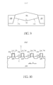
- FIG. 1 to FIG. 8 are schematic diagrams showing a method for fabricating a semiconductor structure according to a first preferred embodiment of the present invention, wherein:
- FIG. 1 to FIG. 5 are 3D schematic diagrams showing the semiconductor structure according to a first preferred embodiment of the present invention.
- FIG. 6 to FIG. 8 are cross section schematic diagrams showing the semiconductor structure according to a first preferred embodiment of the present invention.
- FIG. 9 shows the cross section diagram of the semiconductor structure according to another embodiment of the present invention.
- FIG. 10 shows the cross section diagram of the semiconductor structure according to another embodiment of the present invention.
- FIG. 1 to FIG. 8 are schematic diagrams showing a method for fabricating a semiconductor structure according to a first preferred embodiment of the present invention. Please refer to FIG. 1 .
- FIG. 1 is a schematic diagram showing a semiconductor structure at the beginning of the fabrication process. As this stage, a semiconductor structure having a substrate 100 and a plurality of fin structures 112 disposed thereon is provided.
- the substrate 100 may be chosen from semiconductor substrate such as a bulk silicon substrate, a silicon containing substrate, a III-V semiconductor-on-silicon (such as GaAs-on-silicon) substrate, a graphene-on-silicon substrate, a silicon-on-insulator (SOI) substrate, a silicon dioxide substrate, an aluminum oxide substrate, a sapphire substrate, a germanium containing substrate or an alloy of silicon and germanium substrate.
- semiconductor substrate such as a bulk silicon substrate, a silicon containing substrate, a III-V semiconductor-on-silicon (such as GaAs-on-silicon) substrate, a graphene-on-silicon substrate, a silicon-on-insulator (SOI) substrate, a silicon dioxide substrate, an aluminum oxide substrate, a sapphire substrate, a germanium containing substrate or an alloy of silicon and germanium substrate.
- semiconductor substrate such as a bulk silicon substrate, a silicon containing substrate, a III-V semiconductor-on-silicon (such as GaAs-on-
- the method for fabricating the fin-shaped structures 112 may include the following processes, but not limited thereto. First, a bulk substrate (not shown) is provided and a hard mask layer (not shown) is formed thereon. The hard mask layer is then patterned through a photolithographic and an etching process (photo-etching process), so as to define the location for forming fin structures 112 in the bulk substrate. Afterwards, an etching process is performed to form fin structures 112 in the bulk substrate. After the above processes, the fabrication method for the fin structures 112 is complete. In this case, the fin structures 112 may be regarded as protruding from the surface of the substrate 100 and the compositions of the fin structures 112 and the substrate 100 may be the same, such as monocrystalline silicon.
- the main compositions of the fin-shaped structures may be the same as that of the III-V semiconductor and differ from that of the underlying substrate.
- a photo-etching process P 2 is then performed, to remove parts of the fin structure 112 , and so as to form a plurality of fin structures 114 which are separated from each other.
- another hard mask (not shown) can be formed on the substrate, and the hard mask preferably consists of a plurality of strip-shaped photoresist patterns arranged parallel to each other, wherein the extending direction of each strip-shaped photoresist pattern is preferably perpendicular to the extending direction of each fin structure 112 . Therefore, after the etching process is performed, each fin structure 112 will be segmented into a plurality of fin structures 114 which are separated from each other.
- the removing region of the fin structure 112 is the region that an epitaxial layer will be formed in the following steps. It will be described again in the following paragraphs.
- parts of the fin structure may be regarded as the dummy fin structure (such as the dummy fin structure 112 a shown in FIG. 2 ), and the dummy fin structure 112 a will not be etched.
- the fin structures 112 are formed, another photo-etching process P 2 is then formed to remove parts of the fin structures 112 , so as to form the fin structures 114 .
- an etching process can be performed to remove parts of the photoresist patterns, thereby forming a plurality of hard masks separated from each other.
- another etching process is then performed, so as to transfer the patterns of the rest of the hard masks to the substrate 100 , and the fin structure 114 shown in FIG. 2 can be formed.
- the hard masks mentioned above can be formed on the substrate through a sidewalls image transfer (SIT) process. It is a well-known technology and will not be redundantly described here.
- SIT sidewalls image transfer
- a photoresist layer (not shown) is used as the hard mask to perform a fin-cut process.
- a photoresist layer (not shown) is used as the hard mask to perform a fin-cut process.
- the recess 116 will be filled in the isolation layer in the following steps, so as to form shallow trench isolation (STI).
- the region A 1 which surrounded by the recess 116 can be defined as the active area of the semiconductor device, namely the region comprising the semiconductor device such as transistors disposed therein.
- a flat isolation layer 120 is entirely formed on the substrate 110 , covering each fin structure 114 and also filling in the recess 116 .
- the isolation layer 120 comprises isolating materials such as silicon oxide or silicon nitride. It is noteworthy that the thickness of the isolation layer 120 within the active area A 1 is smaller than the thickness of each fin structure 114 . More precisely, in the present invention, the isolation layer 120 disposed between each of the fin structures 114 can be defined as a first isolation region 122 , and the isolation layer 120 disposed in the recess 116 can be defined as a second isolation region 124 , the depth D 2 of the second isolation region 124 being larger than the depth D 1 of the first isolation region 122 . In addition, before the isolation layer 120 is formed, a liner can be selectively formed between the substrate and the isolation layer 120 , and it should also be within the scope of the present invention.
- Each gate structure 130 includes a gate dielectric layer 132 , a gate conductive layer 134 and a cap layer 136 .
- the material of the gate dielectric layer 132 may include silicon oxide (SiO), silicon nitride (SiN), silicon oxynitride (SiON), or a high-k dielectric material having a dielectric constant (k value) larger than 4 such as metallic oxide, such as hafnium oxide (HfO 2 ), hafnium silicon oxide (HfSiO 4 ), hafnium silicon oxynitride (HfSiON), aluminum oxide (Al 2 O 3 ), lanthanum oxide (La 2 O 3 ), tantalum oxide (Ta 2 O 5 ), yttrium oxide (Y 2 O 3 ), zirconium oxide (ZrO 2 ), strontium titanate oxide (SrTiO 3 ), zirconium silicon oxide (ZrSiO 4 ), hafnium zirconium oxide (HfZrO 4 ), strontium bismuth tantalate (SrBi 2 Ta2O 9 , SBT), lead zirconate titanate
- the material of the gate conductive layer 134 may include undoped polysilicon, heavily doped polysilicon, or one or a plurality of metal layers such as a work function metal layer, a barrier layer and a low-resistance metal layer, etc.
- the cap layer 136 may include a single-layer structure or multi-layer structure made of dielectric materials such as silicon oxide (SiO), silicon nitride (SiN), silicon carbide (SiC), silicon carbonitride (SiCN), silicon oxynitride (SiON) or a combination thereof.
- spacers should also be comprised and disposed on two sides of the gate structure 130 , but in order to simplify the figure, spacers are not shown in FIG. 5 , but it will be described in the following paragraphs and shown in FIG. 6 .
- FIG. 6 show the cross section diagrams along the cross section line A-A′ and along the cross section line B-B′ of FIG. 5 respectively.
- the cross section diagrams along the cross section line A-A′ is the X-direction cross section diagram
- the cross section diagrams along the cross section line B-B′ is the Y-direction cross section diagram.
- the following figures are shown in cross section views, the relative position of each element can be known by referring the FIGS. 5-6 .
- the spacers 138 are shown in the Y-direction cross section diagram of FIG. 6 .
- FIG. 7 shows the cross section diagram of the present invention after performing an epitaxial recess etching process.
- a patterned photoresist layer (not shown) is formed on the isolation layer 120 .
- the patterned photoresist layer includes a plurality of openings, each opening disposed between two adjacent gate structures 130 , and afterwards, an etching process P 4 is then performed, to form the recesses 140 on two sides of each gate structure 130 .
- the bottom surface 142 of the recess 140 may lower than the top surface of the substrate 110 within the active area A 1 .
- the bottom surface 142 of the recess 140 is lower than the bottom surface of the fin structure 114 .
- the recess 140 when viewed in X-direction cross section diagram (along the cross section line A-A′), the recess 140 has two sidewalls 144 , the angle t 1 between the bottom surface 142 and the sidewall 144 is preferably larger than 90 degrees, but not limited thereto.
- the shapes of the recess can be adjusted according to actual requirements.
- FIG. 8 shows the cross section diagram of the present invention after performing a selective epitaxy growing process.
- a selective epitaxy growing (SEG) process P 5 is performed to form an epitaxial layer 150 in the recess 140 , and the epitaxial layer 150 fills up the recess 140 .
- SEG selective epitaxy growing
- the epitaxial layer 150 is to grow along each surface of the recess 140 . Therefore, the epitaxial layer 150 has a bottom surface 152 , and the bottom surface 152 is lower than the top surface 120 a of the isolation layer 120 (it is also the top surface of the second isolation region 124 ).
- the bottom surface 152 is also lower than the bottom surface of the isolation layer 122 (please also refer to FIG. 6 ).
- the angle between the flat bottom surface 152 of the epitaxial layer 150 and the sidewall 154 is preferably larger than 90 degrees. It is noteworthy that the epitaxial layer 150 disposed on sidewalls of each fin structure 114 , and the bottom surface 152 at least extends through more than two fin structures 114 . In other words, the bottom surface 152 of the epitaxial layer 150 disposed in the substrate 110 , and the epitaxial layer 150 directly contacts more than two fin structures 114 .
- the epitaxial layer 150 has a flat bottom surface 152 .
- FIG. 9 shows the cross section diagram of the semiconductor structure according to another embodiment of the present invention.
- the bottom surface 152 a of the epitaxial layer 150 a it is not a flat surface and has an angle t 2 . It should also be within the scope of the present invention.
- the epitaxial layer 150 , 150 a may include a silicon-germanium epitaxial layer suited for a PMOS transistor, or a silicon-carbide epitaxial layer suited for an NMOS transistor, depending upon the electrical properties of the Multi-gate MOSFET.
- the epitaxial layer 150 , 150 a is formed in the recess R, and grows conformally along the shape of the recess R, therefore having a hexagon-shaped profile structure. Thereafter, an ion implantation process may be performed to dope impurities, or impurities may be doped while performing the SEG process P 5 , so that the epitaxial layer 150 can be used as a source/drain region.
- a silicide process (or a salicide process, not shown) may be performed to form silicide in the source/drain region, wherein the silicide process may include a post clean process, a metal depositing process, an annealing process, a selective etching process, or a test process, etc. Thereafter, other processes may be performed after the silicide process is performed.
- FIG. 10 shows the cross section diagram of the semiconductor structure according to another embodiment of the present invention.
- the substrate 210 comprises a plurality of fin structures 214 and a plurality of gate structures 230 disposed thereon, each gate structure 230 includes the cap layer 236 disposed on the top of the gate structure 230 , and the spacers 238 disposed on two sidewalls of the gate structure 230 .
- the epitaxial layers 250 are disposed on two sides of every gate structure 230 .
- the middle line M of one fin structure 214 is regarded as the symmetry axis, and each fin structure 214 is covered by the gate structure 230 asymmetrically.
- the distances between the central point of the gate structure 230 and two ends of the fin structure 214 are labeled as “a” and “b” respectively, and the value a and value b are different. Therefore, the two epitaxial layers 250 disposed on two sides of the gate structure 230 (especially the gate structure disposed near the edges of the active area) may have different volumes.
- the opening of the photoresist layer may be larger than the gap between every two adjacent gate structure 230 , so as to perform a self-aligned etching by using the spacer 238 of the gate structure 230 and/or the cap layer 236 .
- partial sidewall of the fin structure 214 may also be removed, and the fin structure 214 will have a stepped-shaped sidewall profile, since the epitaxial layer 250 grows along each surface of the recess, so the epitaxial layer 250 will also have a stepped-shaped sidewall profile (such as the angle t 3 shown in FIG. 10 ).
- the first embodiment of the present invention mentioned above may also include the stepped-shaped sidewall profile of this embodiment, and will not be described again.
- each fin structure is partially removed during the process for forming the fin structure, and the removed region is used for growing the epitaxial layer.
- the quality of the epitaxial layer can be increased, thereby improving the semiconductor device performance.
- the epitaxial layer of the present invention contacts more than one fin structure. In other words, the source/drain regions of a plurality of transistors can be formed simultaneously, and further improves the convenience of the process.
Landscapes
- Engineering & Computer Science (AREA)
- Power Engineering (AREA)
- Microelectronics & Electronic Packaging (AREA)
- General Physics & Mathematics (AREA)
- Physics & Mathematics (AREA)
- Computer Hardware Design (AREA)
- Condensed Matter Physics & Semiconductors (AREA)
- Manufacturing & Machinery (AREA)
- Ceramic Engineering (AREA)
- Chemical & Material Sciences (AREA)
- Crystallography & Structural Chemistry (AREA)
- Insulated Gate Type Field-Effect Transistor (AREA)
- Chemical Kinetics & Catalysis (AREA)
- General Chemical & Material Sciences (AREA)
Priority Applications (1)
| Application Number | Priority Date | Filing Date | Title |
|---|---|---|---|
| US15/293,292 US9583394B2 (en) | 2015-06-09 | 2016-10-14 | Manufacturing method of semiconductor structure |
Applications Claiming Priority (3)
| Application Number | Priority Date | Filing Date | Title |
|---|---|---|---|
| CN201510311627.3A CN106252391B (zh) | 2015-06-09 | 2015-06-09 | 半导体结构及其制作方法 |
| CN201510311627.3 | 2015-06-09 | ||
| CN201510311627 | 2015-06-09 |
Related Child Applications (1)
| Application Number | Title | Priority Date | Filing Date |
|---|---|---|---|
| US15/293,292 Division US9583394B2 (en) | 2015-06-09 | 2016-10-14 | Manufacturing method of semiconductor structure |
Publications (2)
| Publication Number | Publication Date |
|---|---|
| US9502410B1 true US9502410B1 (en) | 2016-11-22 |
| US20160365344A1 US20160365344A1 (en) | 2016-12-15 |
Family
ID=57287849
Family Applications (2)
| Application Number | Title | Priority Date | Filing Date |
|---|---|---|---|
| US14/792,591 Active US9502410B1 (en) | 2015-06-09 | 2015-07-06 | Semiconductor structure and manufacturing method thereof |
| US15/293,292 Active US9583394B2 (en) | 2015-06-09 | 2016-10-14 | Manufacturing method of semiconductor structure |
Family Applications After (1)
| Application Number | Title | Priority Date | Filing Date |
|---|---|---|---|
| US15/293,292 Active US9583394B2 (en) | 2015-06-09 | 2016-10-14 | Manufacturing method of semiconductor structure |
Country Status (2)
| Country | Link |
|---|---|
| US (2) | US9502410B1 (zh) |
| CN (1) | CN106252391B (zh) |
Cited By (5)
| Publication number | Priority date | Publication date | Assignee | Title |
|---|---|---|---|---|
| US20170179105A1 (en) * | 2015-12-16 | 2017-06-22 | Taiwan Semiconductor Manufacturing Co., Ltd. | Semiconductor device and layout thereof |
| US20180158935A1 (en) * | 2016-12-07 | 2018-06-07 | Qualcomm Incorporated | Asymmetric gated fin field effect transistor (fet) (finfet) diodes |
| CN108417631A (zh) * | 2017-02-09 | 2018-08-17 | 联华电子股份有限公司 | 鳍状结构旁的绝缘层和移除鳍状结构的方法 |
| US10707845B2 (en) * | 2018-11-13 | 2020-07-07 | Marvell International Ltd. | Ultra-low voltage level shifter |
| US20220328627A1 (en) * | 2021-04-08 | 2022-10-13 | Taiwan Semiconductor Manufacturing Co., Ltd. | Semiconductor device and methods of forming the same |
Families Citing this family (3)
| Publication number | Priority date | Publication date | Assignee | Title |
|---|---|---|---|---|
| KR102352155B1 (ko) * | 2015-04-02 | 2022-01-17 | 삼성전자주식회사 | 반도체 소자 및 그 제조방법 |
| US9917154B2 (en) * | 2016-06-29 | 2018-03-13 | International Business Machines Corporation | Strained and unstrained semiconductor device features formed on the same substrate |
| US9941150B1 (en) | 2017-04-27 | 2018-04-10 | International Business Machines Corporation | Method and structure for minimizing fin reveal variation in FinFET transistor |
Citations (8)
| Publication number | Priority date | Publication date | Assignee | Title |
|---|---|---|---|---|
| US20120049294A1 (en) * | 2010-07-26 | 2012-03-01 | Taiwan Semiconductor Manufacturing Company, Ltd. | Forming Crown Active Regions for FinFETs |
| US8410544B2 (en) | 2009-09-17 | 2013-04-02 | International Business Machines Corporation | finFETs and methods of making same |
| US8426923B2 (en) | 2009-12-02 | 2013-04-23 | Taiwan Semiconductor Manufacturing Company, Ltd. | Multiple-gate semiconductor device and method |
| US20140124860A1 (en) * | 2012-11-07 | 2014-05-08 | International Business Machines Corporation | Method and structure for forming a localized soi finfet |
| US20160163851A9 (en) * | 2010-05-28 | 2016-06-09 | Taiwan Semiconductor Manufacturing Company, Ltd. | Structure and method for providing line end extensions for fin-type active regions |
| US20160190305A1 (en) * | 2014-12-30 | 2016-06-30 | Taiwan Semiconductor Manufacturing Company, Ltd. | Structure and Method for 3D FinFET Metal Gate |
| US20160190262A1 (en) * | 2014-12-29 | 2016-06-30 | Globalfoundries Inc. | Confined early epitaxy with local interconnect capability |
| US20160225906A1 (en) * | 2015-02-04 | 2016-08-04 | Taiwan Semiconductor Manufacturing Co., Ltd | Semiconductor device structure and method for forming the same |
Family Cites Families (8)
| Publication number | Priority date | Publication date | Assignee | Title |
|---|---|---|---|---|
| US7309626B2 (en) * | 2005-11-15 | 2007-12-18 | International Business Machines Corporation | Quasi self-aligned source/drain FinFET process |
| US7977174B2 (en) * | 2009-06-08 | 2011-07-12 | Globalfoundries Inc. | FinFET structures with stress-inducing source/drain-forming spacers and methods for fabricating the same |
| US8440517B2 (en) * | 2010-10-13 | 2013-05-14 | Taiwan Semiconductor Manufacturing Company, Ltd. | FinFET and method of fabricating the same |
| US8609499B2 (en) * | 2012-01-09 | 2013-12-17 | Taiwan Semiconductor Manufacturing Company, Ltd. | FinFETs and the methods for forming the same |
| US20130200455A1 (en) * | 2012-02-08 | 2013-08-08 | Taiwan Semiconductor Manufacturing Company, Ltd. | Dislocation smt for finfet device |
| CN103632977B (zh) * | 2012-08-29 | 2016-02-17 | 中芯国际集成电路制造(上海)有限公司 | 半导体结构及形成方法 |
| KR102021768B1 (ko) * | 2013-03-15 | 2019-09-17 | 삼성전자 주식회사 | 반도체 장치의 제조 방법 및 그 방법에 의해 제조된 반도체 장치 |
| US8853015B1 (en) * | 2013-04-16 | 2014-10-07 | United Microelectronics Corp. | Method of forming a FinFET structure |
-
2015
- 2015-06-09 CN CN201510311627.3A patent/CN106252391B/zh active Active
- 2015-07-06 US US14/792,591 patent/US9502410B1/en active Active
-
2016
- 2016-10-14 US US15/293,292 patent/US9583394B2/en active Active
Patent Citations (8)
| Publication number | Priority date | Publication date | Assignee | Title |
|---|---|---|---|---|
| US8410544B2 (en) | 2009-09-17 | 2013-04-02 | International Business Machines Corporation | finFETs and methods of making same |
| US8426923B2 (en) | 2009-12-02 | 2013-04-23 | Taiwan Semiconductor Manufacturing Company, Ltd. | Multiple-gate semiconductor device and method |
| US20160163851A9 (en) * | 2010-05-28 | 2016-06-09 | Taiwan Semiconductor Manufacturing Company, Ltd. | Structure and method for providing line end extensions for fin-type active regions |
| US20120049294A1 (en) * | 2010-07-26 | 2012-03-01 | Taiwan Semiconductor Manufacturing Company, Ltd. | Forming Crown Active Regions for FinFETs |
| US20140124860A1 (en) * | 2012-11-07 | 2014-05-08 | International Business Machines Corporation | Method and structure for forming a localized soi finfet |
| US20160190262A1 (en) * | 2014-12-29 | 2016-06-30 | Globalfoundries Inc. | Confined early epitaxy with local interconnect capability |
| US20160190305A1 (en) * | 2014-12-30 | 2016-06-30 | Taiwan Semiconductor Manufacturing Company, Ltd. | Structure and Method for 3D FinFET Metal Gate |
| US20160225906A1 (en) * | 2015-02-04 | 2016-08-04 | Taiwan Semiconductor Manufacturing Co., Ltd | Semiconductor device structure and method for forming the same |
Cited By (11)
| Publication number | Priority date | Publication date | Assignee | Title |
|---|---|---|---|---|
| US20170179105A1 (en) * | 2015-12-16 | 2017-06-22 | Taiwan Semiconductor Manufacturing Co., Ltd. | Semiconductor device and layout thereof |
| US10163882B2 (en) * | 2015-12-16 | 2018-12-25 | Taiwan Semiconductor Manufacturing Co., Ltd. | Semiconductor device and layout thereof |
| US10854593B2 (en) | 2015-12-16 | 2020-12-01 | Taiwan Semiconductor Manufacturing Co., Ltd. | Semiconductor device and layout thereof |
| US20180158935A1 (en) * | 2016-12-07 | 2018-06-07 | Qualcomm Incorporated | Asymmetric gated fin field effect transistor (fet) (finfet) diodes |
| WO2018106315A1 (en) * | 2016-12-07 | 2018-06-14 | Qualcomm Incorporated | Asymmetric gated fin field effect transistor (fet) (finfet) diodes |
| US10340370B2 (en) | 2016-12-07 | 2019-07-02 | Qualcomm Incorporated | Asymmetric gated fin field effect transistor (FET) (finFET) diodes |
| CN110036487A (zh) * | 2016-12-07 | 2019-07-19 | 高通股份有限公司 | 非对称栅控鳍式场效应晶体管(FET)(finFET)二极管 |
| CN108417631A (zh) * | 2017-02-09 | 2018-08-17 | 联华电子股份有限公司 | 鳍状结构旁的绝缘层和移除鳍状结构的方法 |
| CN108417631B (zh) * | 2017-02-09 | 2022-06-03 | 联华电子股份有限公司 | 鳍状结构旁的绝缘层和移除鳍状结构的方法 |
| US10707845B2 (en) * | 2018-11-13 | 2020-07-07 | Marvell International Ltd. | Ultra-low voltage level shifter |
| US20220328627A1 (en) * | 2021-04-08 | 2022-10-13 | Taiwan Semiconductor Manufacturing Co., Ltd. | Semiconductor device and methods of forming the same |
Also Published As
| Publication number | Publication date |
|---|---|
| US20160365344A1 (en) | 2016-12-15 |
| CN106252391A (zh) | 2016-12-21 |
| CN106252391B (zh) | 2021-02-19 |
| US20170033015A1 (en) | 2017-02-02 |
| US9583394B2 (en) | 2017-02-28 |
Similar Documents
| Publication | Publication Date | Title |
|---|---|---|
| US9337193B2 (en) | Semiconductor device with epitaxial structures | |
| US11972984B2 (en) | Semiconductor device and method for fabricating the same | |
| US9583394B2 (en) | Manufacturing method of semiconductor structure | |
| US10062604B2 (en) | Semiconductor device and method for fabricating the same | |
| US8174073B2 (en) | Integrated circuit structures with multiple FinFETs | |
| US9666715B2 (en) | FinFET transistor with epitaxial structures | |
| US9318609B2 (en) | Semiconductor device with epitaxial structure | |
| US10256240B2 (en) | Semiconductor device having fin-shaped structure and bump | |
| US9780169B2 (en) | Semiconductor structure having epitaxial layers | |
| US9450094B1 (en) | Semiconductor process and fin-shaped field effect transistor | |
| US10090398B2 (en) | Manufacturing method of patterned structure of semiconductor | |
| US20230386939A1 (en) | Semiconductor device and method for fabricating the same | |
| US10566244B2 (en) | Semiconductor device and method for fabricating the same | |
| US9461147B2 (en) | Semiconductor structure | |
| US20210210628A1 (en) | Semiconductor device | |
| US9614034B1 (en) | Semiconductor structure and method for fabricating the same | |
| US9508715B1 (en) | Semiconductor structure |
Legal Events
| Date | Code | Title | Description |
|---|---|---|---|
| AS | Assignment |
Owner name: UNITED MICROELECTRONICS CORP., TAIWAN Free format text: ASSIGNMENT OF ASSIGNORS INTEREST;ASSIGNORS:FENG, LI-WEI;TSAI, SHIH-HUNG;LIU, HON-HUEI;AND OTHERS;SIGNING DATES FROM 20150525 TO 20150630;REEL/FRAME:036003/0128 |
|
| STCF | Information on status: patent grant |
Free format text: PATENTED CASE |
|
| MAFP | Maintenance fee payment |
Free format text: PAYMENT OF MAINTENANCE FEE, 4TH YEAR, LARGE ENTITY (ORIGINAL EVENT CODE: M1551); ENTITY STATUS OF PATENT OWNER: LARGE ENTITY Year of fee payment: 4 |
|
| AS | Assignment |
Owner name: MARLIN SEMICONDUCTOR LIMITED, IRELAND Free format text: ASSIGNMENT OF ASSIGNORS INTEREST;ASSIGNOR:UNITED MICROELECTRONICS CORPORATION;REEL/FRAME:056991/0292 Effective date: 20210618 |
|
| MAFP | Maintenance fee payment |
Free format text: PAYMENT OF MAINTENANCE FEE, 8TH YEAR, LARGE ENTITY (ORIGINAL EVENT CODE: M1552); ENTITY STATUS OF PATENT OWNER: LARGE ENTITY Year of fee payment: 8 |