US9501199B2 - Touch window and touch device including the same - Google Patents
Touch window and touch device including the same Download PDFInfo
- Publication number
- US9501199B2 US9501199B2 US14/468,638 US201414468638A US9501199B2 US 9501199 B2 US9501199 B2 US 9501199B2 US 201414468638 A US201414468638 A US 201414468638A US 9501199 B2 US9501199 B2 US 9501199B2
- Authority
- US
- United States
- Prior art keywords
- substrate
- sensing electrode
- sub
- touch window
- touch
- Prior art date
- Legal status (The legal status is an assumption and is not a legal conclusion. Google has not performed a legal analysis and makes no representation as to the accuracy of the status listed.)
- Active, expires
Links
Images


Classifications
-
- G—PHYSICS
- G06—COMPUTING OR CALCULATING; COUNTING
- G06F—ELECTRIC DIGITAL DATA PROCESSING
- G06F3/00—Input arrangements for transferring data to be processed into a form capable of being handled by the computer; Output arrangements for transferring data from processing unit to output unit, e.g. interface arrangements
- G06F3/01—Input arrangements or combined input and output arrangements for interaction between user and computer
- G06F3/03—Arrangements for converting the position or the displacement of a member into a coded form
- G06F3/041—Digitisers, e.g. for touch screens or touch pads, characterised by the transducing means
- G06F3/044—Digitisers, e.g. for touch screens or touch pads, characterised by the transducing means by capacitive means
- G06F3/0446—Digitisers, e.g. for touch screens or touch pads, characterised by the transducing means by capacitive means using a grid-like structure of electrodes in at least two directions, e.g. using row and column electrodes
-
- G—PHYSICS
- G06—COMPUTING OR CALCULATING; COUNTING
- G06F—ELECTRIC DIGITAL DATA PROCESSING
- G06F3/00—Input arrangements for transferring data to be processed into a form capable of being handled by the computer; Output arrangements for transferring data from processing unit to output unit, e.g. interface arrangements
- G06F3/01—Input arrangements or combined input and output arrangements for interaction between user and computer
- G06F3/03—Arrangements for converting the position or the displacement of a member into a coded form
- G06F3/041—Digitisers, e.g. for touch screens or touch pads, characterised by the transducing means
- G06F3/045—Digitisers, e.g. for touch screens or touch pads, characterised by the transducing means using resistive elements, e.g. a single continuous surface or two parallel surfaces put in contact
-
- G—PHYSICS
- G06—COMPUTING OR CALCULATING; COUNTING
- G06F—ELECTRIC DIGITAL DATA PROCESSING
- G06F3/00—Input arrangements for transferring data to be processed into a form capable of being handled by the computer; Output arrangements for transferring data from processing unit to output unit, e.g. interface arrangements
- G06F3/01—Input arrangements or combined input and output arrangements for interaction between user and computer
- G06F3/03—Arrangements for converting the position or the displacement of a member into a coded form
- G06F3/041—Digitisers, e.g. for touch screens or touch pads, characterised by the transducing means
- G06F3/0412—Digitisers structurally integrated in a display
-
- G—PHYSICS
- G06—COMPUTING OR CALCULATING; COUNTING
- G06F—ELECTRIC DIGITAL DATA PROCESSING
- G06F3/00—Input arrangements for transferring data to be processed into a form capable of being handled by the computer; Output arrangements for transferring data from processing unit to output unit, e.g. interface arrangements
- G06F3/01—Input arrangements or combined input and output arrangements for interaction between user and computer
- G06F3/03—Arrangements for converting the position or the displacement of a member into a coded form
- G06F3/041—Digitisers, e.g. for touch screens or touch pads, characterised by the transducing means
- G06F3/044—Digitisers, e.g. for touch screens or touch pads, characterised by the transducing means by capacitive means
- G06F3/0443—Digitisers, e.g. for touch screens or touch pads, characterised by the transducing means by capacitive means using a single layer of sensing electrodes
-
- H—ELECTRICITY
- H05—ELECTRIC TECHNIQUES NOT OTHERWISE PROVIDED FOR
- H05K—PRINTED CIRCUITS; CASINGS OR CONSTRUCTIONAL DETAILS OF ELECTRIC APPARATUS; MANUFACTURE OF ASSEMBLAGES OF ELECTRICAL COMPONENTS
- H05K1/00—Printed circuits
- H05K1/02—Details
- H05K1/03—Use of materials for the substrate
- H05K1/0393—Flexible materials
-
- B—PERFORMING OPERATIONS; TRANSPORTING
- B82—NANOTECHNOLOGY
- B82Y—SPECIFIC USES OR APPLICATIONS OF NANOSTRUCTURES; MEASUREMENT OR ANALYSIS OF NANOSTRUCTURES; MANUFACTURE OR TREATMENT OF NANOSTRUCTURES
- B82Y10/00—Nanotechnology for information processing, storage or transmission, e.g. quantum computing or single electron logic
-
- G—PHYSICS
- G06—COMPUTING OR CALCULATING; COUNTING
- G06F—ELECTRIC DIGITAL DATA PROCESSING
- G06F2203/00—Indexing scheme relating to G06F3/00 - G06F3/048
- G06F2203/041—Indexing scheme relating to G06F3/041 - G06F3/045
- G06F2203/04103—Manufacturing, i.e. details related to manufacturing processes specially suited for touch sensitive devices
-
- H—ELECTRICITY
- H05—ELECTRIC TECHNIQUES NOT OTHERWISE PROVIDED FOR
- H05K—PRINTED CIRCUITS; CASINGS OR CONSTRUCTIONAL DETAILS OF ELECTRIC APPARATUS; MANUFACTURE OF ASSEMBLAGES OF ELECTRICAL COMPONENTS
- H05K2201/00—Indexing scheme relating to printed circuits covered by H05K1/00
- H05K2201/03—Conductive materials
- H05K2201/032—Materials
- H05K2201/0326—Inorganic, non-metallic conductor, e.g. indium-tin oxide [ITO]
-
- H—ELECTRICITY
- H05—ELECTRIC TECHNIQUES NOT OTHERWISE PROVIDED FOR
- H05K—PRINTED CIRCUITS; CASINGS OR CONSTRUCTIONAL DETAILS OF ELECTRIC APPARATUS; MANUFACTURE OF ASSEMBLAGES OF ELECTRICAL COMPONENTS
- H05K2201/00—Indexing scheme relating to printed circuits covered by H05K1/00
- H05K2201/05—Flexible printed circuits [FPCs]
-
- H—ELECTRICITY
- H05—ELECTRIC TECHNIQUES NOT OTHERWISE PROVIDED FOR
- H05K—PRINTED CIRCUITS; CASINGS OR CONSTRUCTIONAL DETAILS OF ELECTRIC APPARATUS; MANUFACTURE OF ASSEMBLAGES OF ELECTRICAL COMPONENTS
- H05K2201/00—Indexing scheme relating to printed circuits covered by H05K1/00
- H05K2201/10—Details of components or other objects attached to or integrated in a printed circuit board
- H05K2201/10007—Types of components
- H05K2201/10128—Display
-
- Y—GENERAL TAGGING OF NEW TECHNOLOGICAL DEVELOPMENTS; GENERAL TAGGING OF CROSS-SECTIONAL TECHNOLOGIES SPANNING OVER SEVERAL SECTIONS OF THE IPC; TECHNICAL SUBJECTS COVERED BY FORMER USPC CROSS-REFERENCE ART COLLECTIONS [XRACs] AND DIGESTS
- Y10—TECHNICAL SUBJECTS COVERED BY FORMER USPC
- Y10S—TECHNICAL SUBJECTS COVERED BY FORMER USPC CROSS-REFERENCE ART COLLECTIONS [XRACs] AND DIGESTS
- Y10S977/00—Nanotechnology
- Y10S977/902—Specified use of nanostructure
- Y10S977/932—Specified use of nanostructure for electronic or optoelectronic application
- Y10S977/952—Display
Definitions
- the disclosure relates to a touch window and a touch device including the same.
- a touch window which performs an input function through the touch of an image displayed on a touch device by an input device such as a stylus pen or a hand, has been applied to various electronic appliances.
- the touch window may be typically classified into a resistive touch window and a capacitive touch window.
- the position of the touch point is detected by detecting the variation of resistance according to the connection between electrodes when pressure is applied to an input device.
- the capacitive touch window the position of the touch point is detected by detecting the variation in capacitance when a finger of the user touches the capacitive touch window between electrodes.
- the embodiment is to provide a touch window which is flexible, and a touch device including the same.
- the touch window according to the embodiment includes first and second areas, wherein the second area is bendable from the first area.
- the embodiment may provide a touch window of which the structure may be modified in various structures. That is, a wide screen may be provided when a touch window is used, and a size of the touch window may be greatly reduced through the second area when the touch window is carried. Thus, a large size of screen and portability may be secured together.
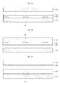
- FIG. 1 is a plan view showing a touch window according to an embodiment.
- FIG. 2 is a sectional view taken along line I-I′ of FIG. 1 .
- FIG. 3 is a sectional view showing a touch window according to another embodiment.
- FIGS. 4 and 5 are plan views showing a touch window according to another embodiment.
- FIGS. 6 and 7 are sectional views taken along line II-II′ of FIG. 5 .
- FIG. 8 is a plan view showing a touch window according to another embodiment.
- FIG. 9 is a sectional view taken along line III-III′ of FIG. 8 .
- FIGS. 10 and 11 are schematic plan views showing a touch window according to another embodiment.
- FIGS. 12 to 17 are sectional views showing a touch device in which the touch window according to the embodiment is disposed on a display panel according to various embodiments.
- each layer shown in the drawings may be exaggerated, omitted or schematically drawn for the purpose of convenience or clarity.
- the size of elements does not utterly reflect an actual size.
- FIG. 1 is a plan view showing the touch window according to the embodiment.
- FIG. 2 is a sectional view taken along line I-I′ of FIG. 1 .
- FIG. 3 is a sectional view showing a touch window according to another embodiment.
- the touch window may include a substrate including first and second areas 1 A and 2 A.
- the substrate 101 may include a first substrate 101 including the first area 1 A and a second substrate 102 including the second area 2 A.
- the first and second substrates 101 and 102 may be formed integrally with each other.
- the first area 1 A may be fixed in the touch window.
- a first sensing electrode 210 and a first wire 310 may be provided on the first substrate 101 including the first area 1 A.
- the first substrate 101 may be formed of various materials which may support the first sensing electrode 210 and the first wire 310 which are formed on the first substrate 101 .
- the first substrate 101 may include a glass substrate or a plastic substrate including a polyethylene terephthalate (PET) film or resin.
- PET polyethylene terephthalate
- the first sensing electrode 210 may include a first material.
- the first material may include transparent conductive film.
- the first material may include metal oxide such as indium tin oxide, indium zinc oxide, copper oxide, tin oxide, zinc oxide or titanium oxide.
- the first material may be a material very useful for visibility without interrupting transmission of light.
- the first wire 310 is electrically connected to the first sensing electrode 210 .
- the first wire 310 may be connected to at least one of ends of the first sensing electrode 210 .
- the first wire 310 may be formed of metal having superior electric conductivity.
- the first wire 310 may include chrome (Cr), nickel (Ni), copper (Cu), aluminum (Al), silver (Ag), molybdenum (Mo), and an alloy thereof.
- the first wire 310 may include various metallic paste materials which can be formed through a printing process.
- the second substrate 102 may be disposed to be adjacent to the first substrate 101 . That is, the second area 2 A may be disposed to be adjacent to the first area 1 A.
- the second substrate 102 may be warped or bent from the first substrate 101 . That is, the second area 2 A may be bent from the first area 1 A.
- the second area 2 A may be bent from the first area 1 A.
- the second area 2 A may be bent downwardly from the first area 1 A.
- the second area 2 A may be bent upwardly from the first area 1 A.
- the second area 2 A may slide from the first area 1 A.
- a second sensing electrode 220 and a second wire 320 may be disposed on the second substrate 102 including the second area 2 A.
- the second substrate 102 may be formed of a plastic substrate including a polyethylene terephthalate (PET) film or resin.
- PET polyethylene terephthalate
- the second substrate 102 may have a flexible property.
- the second sensing electrode 220 may include a second material different from the first material.
- the second material may include an interconnecting structure, a carbon nano tube (CM), graphene or various metals.
- the interconnecting structure may be a micro-structure having a diameter of 10 nm to 200 nm.
- the second sensing electrode 220 may include a nanowire.
- the sensing electrode 220 when the sensing electrode 220 includes a metal, the sensing electrode 220 may include chrome (Cr), nickel (Ni), copper (Cu), aluminum (Al), silver (Ag), molybdenum (Mo) and an alloy thereof.
- the second material has a flexible property so that the second material may be suitable to be applied to the substrate having the bending or warping property.
- the second sensing electrode 220 when the second sensing electrode 220 is formed of a metallic material, the second sensing electrode 220 may include a conductive pattern.
- the second sensing electrode 220 may be disposed in a mesh shape.
- the mesh pattern may be formed in random to prevent a moiré phenomenon.
- the moiré phenomenon occurs when periodical stripes overlap with each other. Since adjacent stripes overlap with each other, a thickness of a stripe is thickened so that the stripe is spotlighted as compared with other stripes.
- the conductive pattern may be provided in various shapes.
- a line width of the mesh line may be in the range of 0.1 ⁇ m to 10 ⁇ m. It may be impossible in terms of the manufacturing process to form the mesh line having the line width less than 0.1 ⁇ m.
- the line width is 10 ⁇ m or less, the pattern of the second sensing electrode 220 may be invisible.
- the line width of the mesh line may be in the range of 1 ⁇ m to 10 ⁇ m about 1 ⁇ m to about 5 ⁇ m or about 1.5 ⁇ m to about 3 ⁇ m.
- the second sensing electrode 220 may include the second material having a flexible property, so that the second sensing electrode 220 may be flexible without any physical damages.
- the second wire 320 is electrically connected to the second sensing electrode 220 .
- the second wire 320 may be connected to at least one of ends of the second sensing electrode 220 .
- the second wire 320 may be formed of metal having superior electric conductivity.
- the second wire 320 may include chrome (Cr), nickel (Ni), copper (Cu), aluminum (Al), silver (Ag), molybdenum (Mo) and an alloy thereof.
- the second wire 320 may include various metallic paste materials which can be formed through a printing process.
- the second wire 320 may be disposed on the flexible second substrate 100 .
- the second wire 320 may be disposed on the second area 2 A.
- only the second wire 320 or the sensing electrode 220 and the second wire 320 together may be disposed on the second area 2 A, that is, the bent area 2 A of the second substrate.
- the embodiment may provide a touch window which may be easily portable and of which the structure may be modified in various structures. That is, a wide screen may be provided when a touch window is used, and a size of the touch window may be greatly reduced through the second area 2 A when the touch window is carried. Thus, a large size of screen and portability may be secured together.
- FIG. 1 shows the sensing electrodes 210 and 220 extending in one direction, but the embodiment is not limited thereto.
- first and second electrode 210 and 220 may include first and second sub-sensing electrodes extending in mutually different directions.
- the first and second sub-sensing electrodes may be disposed in various schemes according to a touch window structure.
- the first and second sub-sensing electrodes may be disposed on the same surface of the substrate.
- the substrate may include a cover substrate including glass or strengthened glass.
- the first and second sub-sensing electrodes may be disposed on the same surface of the cover substrate
- a cover substrate may be further provided on the substrate and the first and second sub-sensing electrodes may be disposed on the same surface of the substrate.
- the first and second sub-sensing electrodes may be disposed on mutually different surfaces of the substrate.
- the first sub-sensing electrode may be disposed on one surface of the substrate and the second sub-sensing electrode may be disposed on the opposite surface of the substrate.
- a middle layer that is, a dielectric layer may be further disposed on the substrate and a cover substrate may be further disposed on the dielectric layer.
- One of the first and second sub-sensing electrodes may be disposed on the substrate and the other may be disposed on the dielectric layer.
- a cover substrate may be further disposed on the substrate.
- One of the first and second sub-sensing electrodes may be disposed on the cover substrate and the other may be disposed on the substrate.
- another substrate may be further disposed on the substrate and a cover substrate may be disposed on the another substrate.
- One of the first and second sub-sensing electrodes may be disposed on the substrate and the other may be disposed on another substrate.
- FIGS. 5 to 7 a touch window according to another embodiment will be described with reference to FIGS. 5 to 7 .
- the parts similar or identical to those of the previously described embodiment will be omitted for the purpose of clear and brief description.
- a touch window according to another embodiment includes two first areas 1 A 1 and 1 A 2 disposed at both sides of the second area 2 A. That is, the second area 2 A, which is flexible, may be interposed between the two first areas 1 A 1 and 1 A 2 .
- a foldable touch window may be implemented.
- the touch window may be used, as shown in FIGS. 5 and 6 , the touch window may be unfolded to use a wide screen.
- the second area 2 A is bent so that the size may be reduced.
- a large size of screen may be secured and at the same time, portability may be ensured.
- the touch window is used or carried, as shown in FIG. 7 , the second area may be bent so that a bent touch window may be implemented.
- FIGS. 8 and 9 a touch window according to still another embodiment will be described.
- the second region 2 A which is a bendable area, surrounds the first area 1 A which is a fixed area. That is, the second area 2 A is disposed at an outside of the first area 1 A. Referring to FIG. 9 , the second area 2 A may be bent from the first area 1 A, so that the grip sensitivity of the touch window may be improved.
- the first and second areas 1 A and 2 A may be variously disposed. That is, as shown in FIG. 10 , the second area 2 A may not be disposed on anyone side surface of the first area 1 A. The second area 2 A may be disposed on three among four side surfaces of the first area 1 A.
- the second area 2 A may be disposed on only two among the four side surfaces of the first area 1 A.
- the embodiment is not limited to the above, but the second area 2 A may be disposed on at least one side surface of the first area 1 A.
- a touch device may include a touch window formed integrally with a display panel 700 .
- a substrate to support at least one sensing electrode may be omitted.
- At least one sub-sensing electrode may be formed on at least one surface of the display panel 700 .
- the display panel 700 includes first and second substrates 701 and 702 .
- at least one sub-sensing electrode may be formed on at least one surface of the first substrate 701 or the second substrate 702 .
- the display panel 700 may be formed in a structure that the first substrate 701 including a thin film transistor (TFT) and a pixel electrode and the second substrate 702 including color filters are combined with each other while interposing a liquid crystal layer therebetween.
- TFT thin film transistor
- the display panel 700 may include a liquid crystal display panel having a color filter on transistor (COT) structure in which a TFT, a color filter, and a black matrix are formed on the first substrate 701 , and the second substrate 702 is combined with the first substrate 701 while interposing a liquid crystal layer between the second substrate 702 and the first substrate 701 .
- the TFT may be formed on the first substrate 701
- a protective layer may be formed on the TFT
- the color filter lay may be formed on the protective layer.
- a pixel electrode making contact with the TFT is formed on the first substrate 701 .
- the black matrix may be omitted to improve an opening ratio and to simplify a mask process, and a common electrode may perform both of the inherent function thereof and the function as the black matrix.
- a display device may further include a backlight unit to provide light to a bottom surface of the display panel 700 .
- the display panel 700 includes a self-emissive device that does not require an additional light source.
- the display panel 700 includes the first substrate 701 formed thereon with a TFT and an organic light emitting device making contact with the TFT.
- the organic light emitting device may include an anode, a cathode, and an organic light emitting layer interposed between the anode and the cathode.
- the second substrate 702 which serves as an encapsulation substrate for encapsulation, may be further provided on the organic light emitting device.
- At least one sub-sensing electrode may be formed on a top surface of an upper substrate.
- the sub-sensing electrode is formed on the top surface of the second substrate 702 in the drawings, when the first substrate 701 serves as the upper substrate, at least one sub-sensing electrode may be formed on the top surface of the first substrate 701 .
- the first sub-sensing electrode 241 may be formed on the top surface of the display panel 700 .
- a first wire connected with the first sub-sensing electrode 241 may be formed.
- a touch substrate 105 having the second sub-sensing electrode 242 and the second wire may be formed on the display panel 700 having the first sub-sensing electrode 241 .
- a first bonding layer 66 may be interposed between the touch substrate 105 and the display panel 700 .
- the drawing shows that the second sub-sensing electrode 242 is formed on the top surface of the touch substrate 105 , and a cover substrate 400 is formed on the touch substrate 105 while interposing a second bonding layer 67 between the touch substrate 105 and the cover substrate 400 , the embodiment is not limited thereto.
- the second sub-sensing electrode 242 may be formed on a bottom surface of the touch substrate 105 .
- the touch substrate 105 may serve as the cover substrate.
- the embodiment is not limited to the structure shown in the drawing, but various modifications are possible if the first sub-sensing electrode 241 is formed on a top surface of the display panel 700 , the touch substrate 105 to support the second sub-sensing electrode 242 is disposed on the display panel 700 , and the touch substrate 105 is combined with the display panel 700 .
- the touch substrate 105 may include a polarizer.
- the second sub-sensing electrode 242 may be formed on top and bottom surfaces of the polarizer. Accordingly, the second sub-sensing electrode 242 may be formed integrally with the polarizer.
- the polarizer may be provided independently from the touch substrate 105 .
- the polarizer may be disposed under the touch substrate 105 .
- the polarizer may be interposed between the touch substrate 105 and the display panel 700 .
- the polarizer may be disposed above the touch substrate 105 .
- the polarizer may include a linear polarizer or an anti-reflective polarizer for external light.
- the polarizer may include the linear polarizer.
- the polarizer may be the anti-reflective polarizer for the external light.
- the first and second sub-sensing electrodes 241 and 242 may be formed on the top surface of the display panel 700 .
- the display panel 700 may be formed on the top surface thereof with the first wire connected with the first sub-sensing electrode 241 and the second wire connected with the second sub-sensing electrode 242 .
- an insulating layer 600 may be formed on the first sub-sensing electrode 241 and expose the second sub-sensing electrode 242 .
- a bridge electrode 230 may be further formed on the insulating layer 600 for the connection between second sub-sensing electrodes 242 .
- the embodiment is not limited to the structure shown in the drawings, and the display panel 700 may be formed on the top surface thereof with the first sub-sensing electrode 241 , the first wire, and the second wire, and the insulating layer may be formed on the first sub-sensing electrode 241 and the first wire.
- the insulating layer may be formed thereon with the second sub-sensing electrode 242 , and a connection part may be further provided to connect the second sub-sensing electrode 242 with the second wire.
- the first and second sub-sensing electrodes 241 and 242 and the first and second wires may be formed in an active area on the top surface of the display panel 700 .
- the first and second sub-sensing electrodes 241 and 242 may be spaced apart from each other while being adjacent to each other. In other words, the insulating layer and the bridge electrode may be omitted.
- the embodiment is not limited to the structure shown in the drawing, but various modifications are possible if the first and second sub-sensing electrodes 241 and 242 are formed on the display panel 700 without an additional sub-sensing electrode support substrate.
- the cover substrate 400 may be disposed above the display panel 700 while a bonding layer 68 is interposed between the display panel 700 and the cover substrate 400 .
- the polarizer may be interposed between the display panel 700 and the cover substrate 400 .
- At least one substrate to support the sub-sensing electrode may be omitted. Accordingly, a thin and light touch device can be formed.
- FIGS. 14 to 17 a touch device according to another embodiment will be described with reference to FIGS. 14 to 17 .
- the details of the same structure and elements as those described above will be omitted.
- the same reference numerals will be assigned to the same elements.
- the touch device may include a touch window formed integrally with a display panel.
- a touch window formed integrally with a display panel.
- at least one or all of substrates to support sensing electrodes may be omitted.
- a sensing electrode disposed at an active area to serve as a sensor, which senses a touch, and a wire to apply an electrical signal to the sub-sensing electrode may be formed inside the display panel.
- at least one sub-sensing electrode or at least one wire may be formed inside the display panel.
- the display panel includes the first and second substrates 701 and 702 .
- at least one of the first and second sub-sensing electrodes 241 and 242 is interposed between the first and second substrates 701 and 702 .
- at least one sub-sensing electrode may be formed on at least one surface of the first substrate 701 or the second substrate 702 .
- the first and second sub-sensing electrodes 241 and 242 and first and second wires may be interposed between the first and second substrates 701 and 702 .
- the first and second sub-sensing electrodes 241 and 242 and the first and second wires may be disposed inside the display panel.
- the first sub-sensing electrode 241 and the first wire may be formed on the top surface of the first substrate 701 of the display panel, and the second sub-sensing electrode 242 and the second wire may be formed on the bottom surface of the second substrate 702 .
- the first and second sub-sensing electrodes 241 and 242 and the first and second wires may be formed on the top surface of the first substrate 701 .
- An insulating layer 620 may be interposed between the first and second sub-sensing electrodes 241 and 242 .
- the first and second sub-sensing electrodes 241 and 242 may be formed on the bottom surface of the second substrate 702 .
- An insulating layer 630 may be interposed between the first and second sub-sensing electrodes 241 and 242 .
- the first sub-sensing electrode 241 and the first wire may be interposed between the first and second substrates 701 and 702 .
- the second sub-sensing electrode 242 and the second wire may be formed on a touch substrate 106 .
- the touch substrate 106 may be disposed on the display panel including the first and second substrates 701 and 702 .
- the first sub-sensing electrode 241 and the first wire may be disposed inside the display panel, and the second sub-sensing electrode 242 and the second wire may be disposed outside the display panel.
- the first sub-sensing electrode 241 and the first wire may be formed on a top surface of the first substrate 701 or a bottom surface of the second substrate 702 .
- a bonding layer may be interposed between the touch substrate 106 and the display panel.
- the touch substrate 105 may serve as the cover substrate.
- the touch substrate 106 may be formed on a top surface thereof with the second sub-sensing electrode 242 , and may be additionally formed on the top surface thereof with a cover substrate that interposes a bonding layer between the cover substrate and the touch substrate 106 .
- the embodiment is not limited to the structure shown in the drawing, but various modifications are possible if the first sub-sensing electrode 241 and the first wire are disposed inside the display panel, and the second sub-sensing electrode 242 and the second wire are disposed outside the display panel.
- the touch substrate 106 may be the polarizer.
- the second sub-sensing electrode 242 may be formed on top and bottom surfaces of the polarizer. Accordingly, the sensing electrode may be formed integrally with the polarizer.
- the polarizer may be provided independently from the touch substrate 106 .
- the polarizer may be disposed under the touch substrate 106 .
- the polarizer may be interposed between the touch substrate 105 and the display panel 700 .
- the polarizer may be disposed above the touch substrate 106 .
- the sub-sensing electrode may be formed together with a TFT or a pixel electrode.
- a color filter layer may be formed on the sub-sensing electrode or the sub-sensing electrode may be formed on the color filter layer.
- the display panel is an organic electroluminescence display panel, and the sub-sensing electrode is formed on the top surface of the first substrate 701 , the sub-sensing electrode may be formed together with a TFT or an organic light emitting device.
- an additional substrate to support the sub-sensing electrode may be omitted. Accordingly, a thin and light touch device can be formed.
- the sensing electrode and the wire are formed together with devices formed on the display panel, so that the process can be simplified and the costs can be saved.
- the touch window may be applied to a vehicle as well as a mobile terminal, so that the touch window may be applied to a PND (Personal Navigation Display) such as a vehicle navigator.
- the touch window may be applied to a dashboard, so that a CID (Center Information Display) may be implemented.
- the embodiment is not limited to the above, and the display device may be used for various electronic appliances.
- any reference in this specification to “one embodiment,” “an embodiment,” “example embodiment,” etc. means that a particular feature, structure, or characteristic described in connection with the embodiment is included in at least one embodiment of the invention.
- the appearances of such phrases in various places in the specification are not necessarily all referring to the same embodiment.
Landscapes
- Engineering & Computer Science (AREA)
- General Engineering & Computer Science (AREA)
- Theoretical Computer Science (AREA)
- Human Computer Interaction (AREA)
- Physics & Mathematics (AREA)
- General Physics & Mathematics (AREA)
- Microelectronics & Electronic Packaging (AREA)
- Position Input By Displaying (AREA)
- Switches That Are Operated By Magnetic Or Electric Fields (AREA)
Applications Claiming Priority (2)
| Application Number | Priority Date | Filing Date | Title |
|---|---|---|---|
| KR10-2013-0101614 | 2013-08-27 | ||
| KR20130101614A KR20150024572A (ko) | 2013-08-27 | 2013-08-27 | 터치 윈도우 및 이를 포함하는 디스플레이 |
Publications (2)
| Publication Number | Publication Date |
|---|---|
| US20150062465A1 US20150062465A1 (en) | 2015-03-05 |
| US9501199B2 true US9501199B2 (en) | 2016-11-22 |
Family
ID=51429050
Family Applications (1)
| Application Number | Title | Priority Date | Filing Date |
|---|---|---|---|
| US14/468,638 Active 2034-10-09 US9501199B2 (en) | 2013-08-27 | 2014-08-26 | Touch window and touch device including the same |
Country Status (6)
| Country | Link |
|---|---|
| US (1) | US9501199B2 (enExample) |
| EP (1) | EP2843519B1 (enExample) |
| JP (1) | JP6490925B2 (enExample) |
| KR (1) | KR20150024572A (enExample) |
| CN (1) | CN104423702B (enExample) |
| TW (1) | TWI623872B (enExample) |
Cited By (4)
| Publication number | Priority date | Publication date | Assignee | Title |
|---|---|---|---|---|
| US20160188098A1 (en) * | 2014-12-26 | 2016-06-30 | Lg Innotek Co., Ltd. | Touch window and touch device |
| US20170153153A1 (en) * | 2015-12-01 | 2017-06-01 | Sensitronics, LLC | Metalized polyester film force sensors |
| US11287935B2 (en) | 2016-12-30 | 2022-03-29 | Lg Display Co., Ltd. | Stretchable touchscreen, method for manufacturing the same, and display device using the same |
| US11907465B2 (en) | 2015-06-05 | 2024-02-20 | Apple Inc. | Electronic devices with display and touch sensor structures |
Families Citing this family (14)
| Publication number | Priority date | Publication date | Assignee | Title |
|---|---|---|---|---|
| KR101931771B1 (ko) * | 2012-11-23 | 2019-03-14 | 삼성디스플레이 주식회사 | 유기 발광 표시 장치 |
| CN105446512B (zh) * | 2014-08-08 | 2018-10-26 | 宸鸿科技(厦门)有限公司 | 触控电极结构及应用其的触控面板 |
| CN106155434B (zh) * | 2015-04-03 | 2019-04-26 | 昆山工研院新型平板显示技术中心有限公司 | 一种柔性触控屏及其制备方法 |
| CN106155384B (zh) * | 2015-04-03 | 2019-04-30 | 昆山工研院新型平板显示技术中心有限公司 | 一种柔性触摸显示装置及其制作方法 |
| KR20160127276A (ko) * | 2015-04-24 | 2016-11-03 | 삼성디스플레이 주식회사 | 표시 장치 |
| KR20170018718A (ko) | 2015-08-10 | 2017-02-20 | 삼성전자주식회사 | 비정질 합금을 이용한 투명 전극 및 그 제조 방법 |
| KR101992915B1 (ko) * | 2016-09-30 | 2019-06-25 | 엘지디스플레이 주식회사 | 터치 센서를 가지는 유기 발광 표시 장치 및 그 제조 방법 |
| KR101992916B1 (ko) | 2016-09-30 | 2019-06-25 | 엘지디스플레이 주식회사 | 터치 센서를 가지는 유기 발광 표시 장치 및 그 제조 방법 |
| TWI609294B (zh) * | 2016-12-27 | 2017-12-21 | 財團法人工業技術研究院 | 摺疊式顯示裝置之使用者介面方法 |
| CN108255331B (zh) * | 2016-12-29 | 2024-03-08 | 京东方科技集团股份有限公司 | 柔性触摸屏及制作方法、显示屏及制作方法以及显示设备 |
| US10073294B1 (en) * | 2017-03-31 | 2018-09-11 | Innolux Corporation | Display device |
| KR20200034388A (ko) | 2018-09-21 | 2020-03-31 | 엘지전자 주식회사 | 이동 단말기 |
| CN111752402A (zh) * | 2019-03-28 | 2020-10-09 | 群创光电股份有限公司 | 一种电子装置 |
| KR102813190B1 (ko) * | 2020-06-30 | 2025-05-26 | 엘지디스플레이 주식회사 | 폴더블 표시 장치 |
Citations (12)
| Publication number | Priority date | Publication date | Assignee | Title |
|---|---|---|---|---|
| US20020149572A1 (en) | 2001-04-17 | 2002-10-17 | Schulz Stephen C. | Flexible capacitive touch sensor |
| US20080303782A1 (en) | 2007-06-05 | 2008-12-11 | Immersion Corporation | Method and apparatus for haptic enabled flexible touch sensitive surface |
| US20090153521A1 (en) | 2007-12-14 | 2009-06-18 | Tsinghua University | Touch panel and display device using the same |
| US20120127112A1 (en) | 2010-11-22 | 2012-05-24 | Industrial Technology Research Institute | Flexible projective capacitive touch sensor structure |
| US20130002133A1 (en) * | 2011-06-30 | 2013-01-03 | Jin Dong-Un | Flexible display panel and display apparatus including the flexible display panel |
| US20130181925A1 (en) | 2012-01-18 | 2013-07-18 | Lg Innotek Co., Ltd. | Touch panel |
| US20130265257A1 (en) * | 2012-04-08 | 2013-10-10 | Samsung Electronics Co., Ltd. | Flexible display apparatus and operating method thereof |
| US20130293096A1 (en) * | 2012-05-07 | 2013-11-07 | Sung-ku Kang | Flexible touch screen panel and flexible display device with the same |
| US20140145977A1 (en) * | 2012-11-23 | 2014-05-29 | Samsung Display Co., Ltd. | Flexible touch screen panel and method of manufacturing the same |
| US20140204285A1 (en) * | 2013-01-24 | 2014-07-24 | Hyoung-Wook Jang | Flexible display device having touch and bending sensing function |
| EP2827230A1 (en) | 2013-07-16 | 2015-01-21 | LG Innotek Co., Ltd. | Touch window and touch device including the same |
| US20150029150A1 (en) | 2013-07-29 | 2015-01-29 | Lg Innotek Co., Ltd. | Touch window and touch device the same |
Family Cites Families (7)
| Publication number | Priority date | Publication date | Assignee | Title |
|---|---|---|---|---|
| JP4747747B2 (ja) * | 2005-09-08 | 2011-08-17 | ソニー株式会社 | 入力装置、その製造方法及び電子機器 |
| KR101521219B1 (ko) * | 2008-11-10 | 2015-05-18 | 엘지전자 주식회사 | 플렉서블 디스플레이를 이용하는 휴대 단말기 및 그 제어방법 |
| KR20120072793A (ko) * | 2010-12-24 | 2012-07-04 | 삼성전기주식회사 | 터치스크린 |
| CN102073406A (zh) * | 2010-12-31 | 2011-05-25 | 汕头超声显示器有限公司 | 触摸屏及手持式装置 |
| TW201237720A (en) * | 2011-03-11 | 2012-09-16 | Cando Corp | Thin type flexible capacitive touch device |
| CN205139862U (zh) * | 2013-05-08 | 2016-04-06 | 阿尔卑斯电气株式会社 | 输入装置 |
| WO2014192344A1 (ja) * | 2013-05-28 | 2014-12-04 | シャープ株式会社 | タッチパネル装置、および、タッチパネル付き表示装置 |
-
2013
- 2013-08-27 KR KR20130101614A patent/KR20150024572A/ko not_active Ceased
-
2014
- 2014-08-25 EP EP14182146.2A patent/EP2843519B1/en active Active
- 2014-08-26 TW TW103129355A patent/TWI623872B/zh active
- 2014-08-26 US US14/468,638 patent/US9501199B2/en active Active
- 2014-08-27 CN CN201410428774.4A patent/CN104423702B/zh active Active
- 2014-08-27 JP JP2014172746A patent/JP6490925B2/ja active Active
Patent Citations (14)
| Publication number | Priority date | Publication date | Assignee | Title |
|---|---|---|---|---|
| US20020149572A1 (en) | 2001-04-17 | 2002-10-17 | Schulz Stephen C. | Flexible capacitive touch sensor |
| US20080303782A1 (en) | 2007-06-05 | 2008-12-11 | Immersion Corporation | Method and apparatus for haptic enabled flexible touch sensitive surface |
| US20090153521A1 (en) | 2007-12-14 | 2009-06-18 | Tsinghua University | Touch panel and display device using the same |
| US20120127112A1 (en) | 2010-11-22 | 2012-05-24 | Industrial Technology Research Institute | Flexible projective capacitive touch sensor structure |
| US20130002133A1 (en) * | 2011-06-30 | 2013-01-03 | Jin Dong-Un | Flexible display panel and display apparatus including the flexible display panel |
| US20130181925A1 (en) | 2012-01-18 | 2013-07-18 | Lg Innotek Co., Ltd. | Touch panel |
| US20130265257A1 (en) * | 2012-04-08 | 2013-10-10 | Samsung Electronics Co., Ltd. | Flexible display apparatus and operating method thereof |
| US20130293096A1 (en) * | 2012-05-07 | 2013-11-07 | Sung-ku Kang | Flexible touch screen panel and flexible display device with the same |
| US20140145977A1 (en) * | 2012-11-23 | 2014-05-29 | Samsung Display Co., Ltd. | Flexible touch screen panel and method of manufacturing the same |
| US20140204285A1 (en) * | 2013-01-24 | 2014-07-24 | Hyoung-Wook Jang | Flexible display device having touch and bending sensing function |
| EP2827230A1 (en) | 2013-07-16 | 2015-01-21 | LG Innotek Co., Ltd. | Touch window and touch device including the same |
| US20150022492A1 (en) | 2013-07-16 | 2015-01-22 | Lg Innotek Co., Ltd. | Touch window and touch device including the same |
| US20150029150A1 (en) | 2013-07-29 | 2015-01-29 | Lg Innotek Co., Ltd. | Touch window and touch device the same |
| EP2833235A1 (en) | 2013-07-29 | 2015-02-04 | LG Innotek Co., Ltd. | Flexible touch panel with bendable active area |
Non-Patent Citations (3)
| Title |
|---|
| European Office Action for Application 14 182 146.2 dated Jul. 28, 2016. |
| European Search Report dated Mar. 10, 2015 issued in Application No. 14182146.2. |
| European Search Report dated Nov. 10, 2015 issued in Application No. 14 182 146.2. |
Cited By (6)
| Publication number | Priority date | Publication date | Assignee | Title |
|---|---|---|---|---|
| US20160188098A1 (en) * | 2014-12-26 | 2016-06-30 | Lg Innotek Co., Ltd. | Touch window and touch device |
| US11907465B2 (en) | 2015-06-05 | 2024-02-20 | Apple Inc. | Electronic devices with display and touch sensor structures |
| US12591330B2 (en) | 2015-06-05 | 2026-03-31 | Apple Inc. | Electronic devices with display and touch sensor structures |
| US20170153153A1 (en) * | 2015-12-01 | 2017-06-01 | Sensitronics, LLC | Metalized polyester film force sensors |
| US10352788B2 (en) * | 2015-12-01 | 2019-07-16 | Sensitronics, LLC | Metalized polyester film force sensors |
| US11287935B2 (en) | 2016-12-30 | 2022-03-29 | Lg Display Co., Ltd. | Stretchable touchscreen, method for manufacturing the same, and display device using the same |
Also Published As
| Publication number | Publication date |
|---|---|
| TW201520868A (zh) | 2015-06-01 |
| KR20150024572A (ko) | 2015-03-09 |
| EP2843519A3 (en) | 2015-04-08 |
| US20150062465A1 (en) | 2015-03-05 |
| EP2843519B1 (en) | 2017-05-31 |
| JP6490925B2 (ja) | 2019-03-27 |
| JP2015046165A (ja) | 2015-03-12 |
| EP2843519A2 (en) | 2015-03-04 |
| TWI623872B (zh) | 2018-05-11 |
| CN104423702B (zh) | 2020-04-07 |
| CN104423702A (zh) | 2015-03-18 |
Similar Documents
| Publication | Publication Date | Title |
|---|---|---|
| US9501199B2 (en) | Touch window and touch device including the same | |
| US10353524B2 (en) | Touch window and touch device including the same | |
| US10019124B2 (en) | Touch window | |
| US9823792B2 (en) | Touch panel | |
| US9791981B2 (en) | Touch window and touch device including the same | |
| US10013084B2 (en) | Bendable touch window and touch device with the same | |
| CN204557440U (zh) | 触摸窗 | |
| US9857894B2 (en) | Touch panel having a color film that includes a color part | |
| US20150092359A1 (en) | Touch window and touch device with the same | |
| US10386961B2 (en) | Touch window | |
| US9547397B2 (en) | Touch window and touch device the same | |
| KR20160030635A (ko) | 전극 부재 및 이를 포함하는 터치 윈도우 | |
| KR20170001328A (ko) | 터치 윈도우 | |
| KR20170136758A (ko) | 터치 윈도우 및 터치 디바이스 | |
| KR20160136830A (ko) | 터치 윈도우 |
Legal Events
| Date | Code | Title | Description |
|---|---|---|---|
| AS | Assignment |
Owner name: LG INNOTEK CO., LTD., KOREA, REPUBLIC OF Free format text: ASSIGNMENT OF ASSIGNORS INTEREST;ASSIGNOR:HER, JAE HAK;REEL/FRAME:033609/0809 Effective date: 20140818 |
|
| STCF | Information on status: patent grant |
Free format text: PATENTED CASE |
|
| FEPP | Fee payment procedure |
Free format text: PAYOR NUMBER ASSIGNED (ORIGINAL EVENT CODE: ASPN); ENTITY STATUS OF PATENT OWNER: LARGE ENTITY |
|
| MAFP | Maintenance fee payment |
Free format text: PAYMENT OF MAINTENANCE FEE, 4TH YEAR, LARGE ENTITY (ORIGINAL EVENT CODE: M1551); ENTITY STATUS OF PATENT OWNER: LARGE ENTITY Year of fee payment: 4 |
|
| MAFP | Maintenance fee payment |
Free format text: PAYMENT OF MAINTENANCE FEE, 8TH YEAR, LARGE ENTITY (ORIGINAL EVENT CODE: M1552); ENTITY STATUS OF PATENT OWNER: LARGE ENTITY Year of fee payment: 8 |