US9460886B2 - High resolution high quantum efficiency electron bombarded CCD or CMOS imaging sensor - Google Patents
High resolution high quantum efficiency electron bombarded CCD or CMOS imaging sensor Download PDFInfo
- Publication number
- US9460886B2 US9460886B2 US14/614,088 US201514614088A US9460886B2 US 9460886 B2 US9460886 B2 US 9460886B2 US 201514614088 A US201514614088 A US 201514614088A US 9460886 B2 US9460886 B2 US 9460886B2
- Authority
- US
- United States
- Prior art keywords
- photoelectrons
- vacuum tube
- sensor
- electron
- tube chamber
- Prior art date
- Legal status (The legal status is an assumption and is not a legal conclusion. Google has not performed a legal analysis and makes no representation as to the accuracy of the status listed.)
- Active, expires
Links
- 238000003384 imaging method Methods 0.000 title description 10
- 230000005684 electric field Effects 0.000 claims abstract description 35
- 230000005405 multipole Effects 0.000 claims abstract description 9
- 230000000694 effects Effects 0.000 claims abstract description 8
- 230000003287 optical effect Effects 0.000 claims description 28
- 238000007689 inspection Methods 0.000 claims description 12
- 239000000463 material Substances 0.000 claims description 12
- 238000000034 method Methods 0.000 claims description 12
- 230000004044 response Effects 0.000 claims description 12
- 230000004075 alteration Effects 0.000 claims description 8
- 229910052796 boron Inorganic materials 0.000 claims description 7
- ZOXJGFHDIHLPTG-UHFFFAOYSA-N Boron Chemical compound [B] ZOXJGFHDIHLPTG-UHFFFAOYSA-N 0.000 claims description 5
- 239000011248 coating agent Substances 0.000 claims description 5
- 238000000576 coating method Methods 0.000 claims description 5
- 230000003247 decreasing effect Effects 0.000 claims description 5
- 230000010354 integration Effects 0.000 claims description 3
- 239000003513 alkali Substances 0.000 claims description 2
- 229910001218 Gallium arsenide Inorganic materials 0.000 claims 1
- 238000013459 approach Methods 0.000 abstract description 20
- 230000001133 acceleration Effects 0.000 abstract description 6
- 238000005286 illumination Methods 0.000 description 17
- 238000013461 design Methods 0.000 description 13
- 230000005540 biological transmission Effects 0.000 description 11
- OAICVXFJPJFONN-UHFFFAOYSA-N Phosphorus Chemical compound [P] OAICVXFJPJFONN-UHFFFAOYSA-N 0.000 description 6
- 239000011521 glass Substances 0.000 description 6
- 230000006870 function Effects 0.000 description 5
- 238000000149 argon plasma sintering Methods 0.000 description 4
- JMASRVWKEDWRBT-UHFFFAOYSA-N Gallium nitride Chemical compound [Ga]#N JMASRVWKEDWRBT-UHFFFAOYSA-N 0.000 description 3
- 238000006243 chemical reaction Methods 0.000 description 3
- 238000010586 diagram Methods 0.000 description 3
- 239000004033 plastic Substances 0.000 description 3
- 239000004065 semiconductor Substances 0.000 description 3
- 239000000758 substrate Substances 0.000 description 3
- 101100064589 Arabidopsis thaliana EB1A gene Proteins 0.000 description 2
- 101100064590 Arabidopsis thaliana EB1B gene Proteins 0.000 description 2
- 229910002601 GaN Inorganic materials 0.000 description 2
- 230000008901 benefit Effects 0.000 description 2
- LZDVDTNBLCLMGQ-UHFFFAOYSA-N cesium telluride Chemical compound [Cs][Te][Cs] LZDVDTNBLCLMGQ-UHFFFAOYSA-N 0.000 description 2
- 230000008878 coupling Effects 0.000 description 2
- 238000010168 coupling process Methods 0.000 description 2
- 238000005859 coupling reaction Methods 0.000 description 2
- 239000013078 crystal Substances 0.000 description 2
- 230000007547 defect Effects 0.000 description 2
- 238000011160 research Methods 0.000 description 2
- 229910052710 silicon Inorganic materials 0.000 description 2
- 239000010703 silicon Substances 0.000 description 2
- JBRZTFJDHDCESZ-UHFFFAOYSA-N AsGa Chemical compound [As]#[Ga] JBRZTFJDHDCESZ-UHFFFAOYSA-N 0.000 description 1
- 206010010071 Coma Diseases 0.000 description 1
- 230000004888 barrier function Effects 0.000 description 1
- 230000015572 biosynthetic process Effects 0.000 description 1
- 239000000919 ceramic Substances 0.000 description 1
- 238000005229 chemical vapour deposition Methods 0.000 description 1
- 238000001514 detection method Methods 0.000 description 1
- 238000009792 diffusion process Methods 0.000 description 1
- 239000000835 fiber Substances 0.000 description 1
- 230000004907 flux Effects 0.000 description 1
- 230000006872 improvement Effects 0.000 description 1
- 229910052751 metal Inorganic materials 0.000 description 1
- 239000002184 metal Substances 0.000 description 1
- 238000012986 modification Methods 0.000 description 1
- 230000004048 modification Effects 0.000 description 1
- 238000004382 potting Methods 0.000 description 1
- 230000008569 process Effects 0.000 description 1
- 239000007787 solid Substances 0.000 description 1
- 238000012546 transfer Methods 0.000 description 1
- VLCQZHSMCYCDJL-UHFFFAOYSA-N tribenuron methyl Chemical compound COC(=O)C1=CC=CC=C1S(=O)(=O)NC(=O)N(C)C1=NC(C)=NC(OC)=N1 VLCQZHSMCYCDJL-UHFFFAOYSA-N 0.000 description 1
- 230000000007 visual effect Effects 0.000 description 1
Images


Classifications
-
- H—ELECTRICITY
- H01—ELECTRIC ELEMENTS
- H01J—ELECTRIC DISCHARGE TUBES OR DISCHARGE LAMPS
- H01J31/00—Cathode ray tubes; Electron beam tubes
- H01J31/08—Cathode ray tubes; Electron beam tubes having a screen on or from which an image or pattern is formed, picked up, converted, or stored
- H01J31/26—Image pick-up tubes having an input of visible light and electric output
-
- G—PHYSICS
- G01—MEASURING; TESTING
- G01N—INVESTIGATING OR ANALYSING MATERIALS BY DETERMINING THEIR CHEMICAL OR PHYSICAL PROPERTIES
- G01N21/00—Investigating or analysing materials by the use of optical means, i.e. using sub-millimetre waves, infrared, visible or ultraviolet light
- G01N21/84—Systems specially adapted for particular applications
- G01N21/88—Investigating the presence of flaws or contamination
-
- H—ELECTRICITY
- H01—ELECTRIC ELEMENTS
- H01J—ELECTRIC DISCHARGE TUBES OR DISCHARGE LAMPS
- H01J29/00—Details of cathode-ray tubes or of electron-beam tubes of the types covered by group H01J31/00
- H01J29/46—Arrangements of electrodes and associated parts for generating or controlling the ray or beam, e.g. electron-optical arrangement
-
- H—ELECTRICITY
- H01—ELECTRIC ELEMENTS
- H01L—SEMICONDUCTOR DEVICES NOT COVERED BY CLASS H10
- H01L27/00—Devices consisting of a plurality of semiconductor or other solid-state components formed in or on a common substrate
- H01L27/14—Devices consisting of a plurality of semiconductor or other solid-state components formed in or on a common substrate including semiconductor components sensitive to infrared radiation, light, electromagnetic radiation of shorter wavelength or corpuscular radiation and specially adapted either for the conversion of the energy of such radiation into electrical energy or for the control of electrical energy by such radiation
- H01L27/144—Devices controlled by radiation
- H01L27/146—Imager structures
Definitions
- This invention relates to the field of optical devices and more particularly to electron bombarded imaging sensors.
- An image intensifier tube is a vacuum tube device that increases the intensity of available light in an optical system to facilitate visual imaging of low-light processes, such as fluorescence of materials in x-rays or gamma rays (x-ray image intensifier), or for conversion of non-visible light sources, such as near-infrared or short wave infrared to visible.
- Image intensifiers based on micro-channel plate (MCP) and proximity focus concept can provide high gain due to MCP magnification, low distortion, and uniform resolution across an entire field of view.
- MCP-based image intensifiers tend to have relatively bad resolution for many critical applications.
- MCP may block as much as 40% of the photoelectrons right after the photocathode. Thus, detective quantum efficiency for MCP-based image intensifiers is usually low.
- intensifier tubes based on electrostatic focusing lens or combined magnetic-electrostatic focusing optics may be utilized.
- image intensifier tubes usually have much better detector quantum efficiency (DQE) and resolution than MCP-based image intensifiers.
- DQE detector quantum efficiency
- MCP-based image intensifiers electron and photon scattering in the amorphous phosphor scintillating layer can still degrade the final resolution.
- fiber plate or relay optical lens is required to transfer the light emitted on the phosphor screen to the final imaging device, such as CCD or CMOS. Resolution and gain can be further degraded at this coupling stage.
- high numerical aperture (NA) relay lens may be required.
- High NA and large field of view (FOV) optics require a relay lens with a large diameter and long profile.
- the cost of such relay optics may become significant.
- the shallow depth of focus in such a collection scheme is another concern. All these shortcomings increase the challenges of optical alignment and field service.
- pixelated image sensors such as CCD or CMOS sensors are placed on the phosphor screen location to directly collect photoelectrons emitted from the photocathode.
- CCD electron bombarded CCD
- EBCMOS electron bombarded CMOS
- EBCCD or EBCMOS devices eliminate the electron-to-photon conversion step in phosphor screen and the expensive coupling device between phosphor and CCD or CMOS sensor.
- EBCCD/EBCMOS detectors are designed based on proximity focus method to simplify the design, reduce the power requirements and make the detector compact.
- Proximity focus EBCCD/EBCMOS are disclosed, for example, in U.S. Pat. No. 5,321,334 issued on Jun. 14, 1994 to Katsuyuki Kinoshita and Yoshinori Inagaki, and in U.S. Pat. No. 6,285,018 issued on Sep. 4, 2001 to Verle W. Aebi et al.
- FIG. 1 A conceptual drawing of proximity-focus EBCCD is shown in FIG. 1 .
- a photocathode layer 101 is coated on a glass substrate 100 .
- a CCD/CMOS chip 104 is placed on a package substrate 105 facing photocathode 101 .
- the whole package is sealed by potting material 103 to form a vacuum tight tube.
- Photocathode in traditional EBCCD/EBCMOS device is usually in the form of transmission mode. It means incoming photons will pass through the glass window and illuminate the photocathode layer on the side with interface layer to the glass substrate.
- photoelectrons 102 Upon the incoming photon illumination, photoelectrons 102 are emitted from the vacuum side surface of the photocathode layer, then they will be accelerated by the bias voltage 106 applied between the photocathode layer and the sensor surface.
- narrower gap and higher accelerating bias voltage will result in shorter travel time, thus better resolution.
- narrower gap and higher bias voltage means higher electric field strength between the photocathode and the sensor. If the electric field strength approaches 2 ⁇ 4 kV/mm, the risk of arcing increases significantly depending on the vacuum pressure, surface smoothness and materials. To get a sub-pixel resolution, the gap needs to be so small that non-flatness of CCD/CMOS chip, especially on the back-thinned sensor becomes significant. Such a non-uniform gap may results in variation of resolution, localized distortion and increased risk of arcing.
- electrostatically focused hybrid EBCCD design has been disclosed in U.S. Pat. No. 5,321,334 issued on Jun. 14, 1994 to Katsuyuki Kinoshita et al and a research paper published in Nuclear Instruments and Methods A, issue 2-3, page 255, August 1998 by S. Buontempo et al.
- electrostatic focused vacuum tube usually has poor focus uniformity or non-flat object/image plane and high image distortion.
- Such shortcomings limit its application in high resolution Time Delay Integration (TDI) imaging sensors.
- TDI Time Delay Integration
- distortion may be rendered as blur in TDI mode imaging sensors.
- the overall DQE of an EBCCD/EBCMOS device is mostly determined by the quantum efficiency (QE) of the photocathode.
- QE quantum efficiency
- photons are mostly absorbed on the front side of the photocathode.
- the energetic electrons inside the photocathode layer need to diffuse to the vacuum side of the photocathode before they can escape the energy barrier created by the work function. Momentum of the energetic electrons may be lost during the diffusion process between the two surfaces.
- a reflective mode photocathode photons are absorbed on the vacuum side of the photocathode. Energetic electrons can immediately escape the photocathode close to the same location. Therefore, a reflective mode photocathode usually has significantly higher quantum efficiency.
- reflective mode photocathode can achieve more than 50% to 100% higher quantum efficiency (QE) compared with corresponding transmission mode photocathode.
- QE quantum efficiency
- a research paper published in Proceedings of SPIE vol. 8359 in 2012 by Yoshihiro Ishigami, et al compared the QE of GaN photocathode in reflective mode and transmission mode.
- the QE of GaN photocathode for 266 nm photons can be as high as 37% in reflective mode. Yet the QE will be reduced to 17% in transmission mode. It's almost impossible to implement the reflective mode photocathode in traditional proximity-focus EBCCD/EBCMOS without significantly sacrificing resolution by increasing the tube length.
- a reflective mode oblique magnetic field focused EBCCD/CMOS device had been reported by C. B. Opal and G. R. Carruthers in the Proceedings of SPIE vol. 1158, page 96-103 in 1989 to improve the resolution and quantum efficiency.
- Such a device has a magnetic field tilted with respect to the accelerating electric field axis.
- the oblique magnetic field can deflect the photoelectrons off the normal axis and focus them on to the sensor that is not located on the normal axis.
- the overall device is bulky. Focus aberrations and geometrical distortion in oblique focus design could be too high for many high resolution TDI imaging applications, such as semiconductor defect inspection equipment.
- EBCCD/CMOS device that can achieve high spatial resolution, low landing energy, and high gain. Furthermore there is a need for an EBCCD/CMOS device that can achieve these requirements even if the sensor has many tens of microns or about one hundred microns of non-flatness.
- the present invention is directed to electron-bombarded detectors (e.g., EBCCD or EBCMOS detectors) that utilize various novel structures and methodologies to achieve both high resolution electron optics and low landing energies (e.g., 2 keV or below), thereby providing high quality low light imaging and maximizing the operating lifetime of the CMOS or CCD image sensor.
- EBCCD or EBCMOS detectors electron-bombarded detectors
- EBCMOS detectors electron-bombarded detectors
- ring electrodes are utilized to accelerate the photoelectrons as they leave the photocathode, and a magnetic field generator is utilized to generate a focusing lens effect on the photoelectrons as they pass through a vacuum chamber between the photocathode and the sensor.
- the first approach is to make the distance between the photocathode and the sensor around 10 mm to 20 mm, a distance that is significantly longer than the gap in traditional proximity EBCCD (usually less than 0.5 mm) and significantly shorter than magnetically focused image intensifier with phosphor screen (usually >40 mm), whereby the photoelectrons are accelerated at a relatively low accelerating electric field to generate the desired low landing energy.
- an additional magnetic field generated by a solenoid with current of 3 Amps or less or permanent magnets to achieve high resolution electron optics In this case, an additional magnetic field generated by a solenoid with current of 3 Amps or less or permanent magnets to achieve high resolution electron optics.
- the ring electrodes near the photocathode receive sequentially increasing voltages such that the photoelectrons accelerate to a peak energy within a short distance along vacuum tube chamber, and the ring electrodes near the CCD/CMOS sensor receive sequentially decreasing voltages such that the photoelectrons decelerate from the peak energy to the desired low landing energy.
- both transmission mode embodiments and reflective mode embodiments are disclosed.
- either electric deflection fields or magnetic deflection fields are utilized to deflect the photoelectrons to the off axis sensor.
- one or more of the ring electrodes comprises a segmented circular electrode structure including two or more electrically isolated curved sectors, and different voltages are applied on each curved sector to generate a deflective electric field.
- a multi-pole deflector coil is disposed between the vacuum tube structure and a permanent magnet or a solenoid, where the multi-pole deflector coil configured to generate a deflective magnetic field.
- an electrostatic deflector or a magnetic deflector are utilized to deflect the photoelectrons to an off axis angle larger than about 30 degrees.
- the present invention is also directed to a dark-field inspection system including one or more EB (CCD or CMOS) detectors of the type described above, and an optical system that is configured for directing light to a sample being inspected, for collecting scattered light from the sample, and for directing collected light to the EB detector.
- EB CCD or CMOS
- FIG. 1 is a cross-sectional side view showing a traditional proximity-focus EBCCD
- FIG. 2 is a cross-sectional side view showing a transmission mode magnetic focused EBCCD/EBCMOS according to an embodiment of the present invention
- FIG. 3A is an diagram showing energy of photoelectrons along the tube length in an accelerating tube embodiment
- FIG. 3B is a cross-sectional side view showing a transmission mode magnetic focused EBCCD/EBCMOS having a reduced distance configuration according to an embodiment of the present invention
- FIG. 4 is a diagram showing energy of photoelectrons along the tube length in a decelerating tube embodiment
- FIG. 5 is a cross-sectional side view showing a reflective mode ECCD/EBCMOS with electrostatic deflection according to another embodiment of the present invention.
- FIG. 6(A) is a top view showing a circular ring electrode divided into two electrodes to act as both a dipole deflector and a ring electrode;
- FIG. 6(B) is a top view showing a circular ring electrode divided into six pieces to act as both a sextupole deflector and a ring electrode;
- FIG. 7 is a cross-sectional side view showing a ECCD/EBCMOS with a magnetic field deflection according to another embodiment of the present invention.
- FIG. 8 is a schematic diagram of a large deflection angle reflective mode EBCCD/EBCMOS design
- FIGS. 9A and 9B are top-front perspective and side views, respectively, showing surface inspection apparatus including EBCCD/EBCMOS detectors according to yet other embodiments of the present invention.
- FIG. 10 is a simplified side view showing a dark-field wafer inspection system including a plurality of EBCCD/EBCMOS detectors according to another embodiment of the present invention.
- the present invention relates to an improvement in electron-bombarded detectors for low light signal detection.
- the following description is presented to enable one of ordinary skill in the art to make and use the invention as provided in the context of a particular application and its requirements.
- Various modifications to the preferred embodiment will be apparent to those with skill in the art, and the general principles defined herein may be applied to other embodiments. Therefore, the present invention is not intended to be limited to the particular embodiments shown and described, but is to be accorded the widest scope consistent with the principles and novel features herein disclosed.
- FIG. 2 is a cross-sectional side view showing an electron-bombarded detector (EB-detector) 200 , such as an EB-CCD or an EB-CMOS detector, that illustrates an exemplary transmission mode electron-bombarded detector according to an embodiment of the present invention.
- EB-detector 200 generally includes a vacuum tube structure 201 , a photocathode 101 , a sensor 104 , ring electrodes E 1 to En, a magnetic field generator 210 and a controller 220 .
- Vacuum tube structure 201 includes a cylindrical wall 202 , a first end wall 203 and a second end wall 204 that collectively form (define) a cylindrical vacuum-tight tube chamber 205 having a circular first end 205 - 1 and an opposing circular second end 205 - 2 .
- Cylindrical wall 202 , first end wall 203 and a second end wall 204 are constructed using known rigid materials such as ceramic, silicon, glass or plastic.
- an illumination window 206 e.g., glass, optical crystal or clear plastic
- first end wall 203 is disposed on first end wall 203 .
- Photocathode 101 and sensor 104 are disposed at opposite ends of vacuum tube chamber 205 , with photocathode 101 positioned to generate photoelectrons in response to low light signals (photons), and sensor 104 positioned to capture the emitted photoelectrons after they are accelerated across vacuum tube chamber 205 in the manner described below.
- Photocathode 101 is disposed on an inside surface of first end wall 203 (i.e., at first end 205 - 1 of vacuum tube chamber 205 ) and includes one or more materials that emit photoelectrons in response to said low light signals.
- photocathode 101 includes one or more alkali based materials, gallium-nitride (GaN), or gallium-arsenide (GaAs), or cesium telluride (CsTe), or a combination including two or more of these materials.
- Sensor 104 is disposed at second end 205 - 2 of vacuum tube chamber 205 , and is configured to receive at least some of the emitted photoelectrons and to generate an electric signal S in response to the received photoelectrons.
- sensor 104 is either a charge-coupled device (CCD) image sensor or a CMOS image sensor.
- CCD charge-coupled device
- sensor 104 is of a type configured to generate image information using time-delay integration (TDI), such as a TDI CCD, in order to provide higher speed.
- TDI time-delay integration
- sensor 104 is either a back-thinned CMOS or a back-thinned CCD sensor to increase the photon to photoelectron conversion efficiency and thereby improve low-light performance.
- a boron coating is disposed on a surface of sensor 104 facing towards photocathode 101 to achieve high gain at low landing electron energy and improve the operating lifetime of the sensor. More details on boron coating of sensors can be found in U.S.
- Ring electrodes E 1 to En and magnetic field generator 210 are configured to accelerate the emitted photoelectrons toward sensor 104 , and to focus the accelerated photoelectrons such that they arrive at sensor 104 in a pattern similar to the pattern of their generation.
- Electrodes E 1 , E 2 , E 3 . . . En respectively receive voltages V 1 , V 2 , V 3 . . . Vn from controller 220 , thereby generating an acceleration equipotential profile (indicated by generally vertical long-dashed lines) within the EB-detector 200 that accelerates the emitted photoelectrons towards electron sensor 102 .
- Controller 220 is configured to generate and transmit voltages V 1 , V 2 , V 3 . . . Vn to electrodes E 1 , E 2 , E 3 . . . En such that the voltages (e.g., V 1 and V 2 ) applied on the electrodes adjacent to photocathode 101 (e.g., electrodes E 1 and E 2 ) are adjusted to compensate the electron optics aberrations, for example, by creating a high strength electric near photocathode 101 followed by a relatively low electric field near sensor 104 .
- Such electric field profile creates divergent (negative) lens effect and compensates the positive optics aberrations generated by the magnetic focusing field.
- Magnetic field generator 210 surrounds vacuum tube structure 201 such that the entire tube structure is immersed in an axially symmetric magnetic field ⁇ right arrow over (B) ⁇ (shown as generally horizontal small-dashed lines in FIG. 2 ) that is created by the solenoid coil (e.g., in response to solenoid control current I S generated by controller 220 ) and/or permanent magnets forming magnetic field generator 210 . As indicated in FIG.
- axially symmetric magnetic field ⁇ right arrow over (B) ⁇ is formed such that both photoelectrons emitted from a location off the tube axis (e.g., photoelectrons PE 2 and PE 3 ) and photoelectrons emitted close to the axis (e.g., photoelectron PE 1 ) are brought into focus at the same plane on sensor 104 by adjusting the electric field around photocathode 101 to create a divergent (negative) lens effect to compensate the positive optical aberrations created by the magnetic field.
- low-light signals LLS i.e., illumination
- LLS i.e., illumination
- photocathode 101 to emit photoelectrons (e.g., photoelectrons PE 1 , PE 2 and PE 3 ).
- photoelectrons e.g., photoelectrons PE 1 , PE 2 and PE 3 .
- E electric field ⁇ right arrow over (E) ⁇ generated by electrodes E 1 , E 2 , E 3 . . . En across the space between the photocathode 101 and solid state sensor 104 , and arrive at sensor 104 with a low landing energy while maintaining high resolution electron optics.
- electron-bombarded detector 200 is configured to achieve high resolution electron optics at low landing energy (i.e., such that said photoelectrons arriving at sensor 104 have a landing energy below 2 keV.
- the landing energy of the photoelectrons is usually significantly higher than 20 keV to generate enough photons on the scintillator screen.
- Such a high landing energy can damage CCD or CMOS sensor rapidly in EBCCD/EBCMOS devices.
- the present invention utilizes two basic approaches to obtain high resolution electron optics at low landing energy: a reduced distance approach, which is described below with reference to FIGS. 3A and 3B , and an acceleration/deceleration approach, which is described below with reference to FIG. 4 .
- the reduced distance focusing approach involves reducing the distance between the photocathode plane and the sensor plane while maintaining the accelerating electric field ⁇ in between such that photoelectrons arrive at the sensor plane having a landing energy of 2 keV or less.
- photoelectron energy constantly increases along the flight path between the photocathode plane and the sensor plane. Photoelectrons are accelerated faster and faster until they hit the semiconductor sensor at a landing energy E LE .
- Off axis photoelectrons e.g., photoelectrons PE 2 and PE 3 , shown in FIG. 2
- FIG. 3B illustrates an EB detector 200 A according to one exemplary implementation of the reduced distance focusing approach, where vacuum tube structure 201 A includes a reduced-length cylindrical wall 202 A defining a cylindrical tube chamber 205 A having a radius r that is larger than a distance d between photocathode 101 and sensor 104 .
- radius r is 20 mm
- distance d is 14 mm.
- Controller 220 A applies a current I S of 2.4 amps to a solenoid 211 A of magnetic field generator 210 A (which also includes an optional permanent magnet 212 A), and also applies suitable bias voltages V 1 to V 3 to each ring electrode E 1 to E 3 such that electric field ⁇ is less than 0.25 kV/mm.
- the gap between the photocathode and the sensor may be less than 0.5 mm, and electric field may need to higher than 2.5 kV/mm to achieve reasonable resolution.
- resolution in this reduced length magnetically focusing EBCCD/EBCMOS tube has been improved by 3 ⁇ at a gap that is 30 times larger.
- the electric field in the exemplary device is only 0.086 kV/mm.
- the risk of arcing is negligible.
- the magnetically focused EBCCD/EBCMOS device disclosed in this application totally eliminates the risk of high voltage arcing and achieves much improved resolution.
- the depth of focus of such exemplary EBCCD/EBCMOS device can be more than 100 um, which is large enough to handle the non-flatness of many back-thinned EBCCD/EBCMOS device.
- Non-flatness in back-thinned semiconductor sensor is a serious issue for traditional proximity EBCCD/EBCMOS due to the short gap ( ⁇ 0.5 mm).
- This reduced distance magnetically focusing approach can compensate the field curvature aberrations on the sensor plane.
- Final resolution is very sensitive to the electric field strength around the photocathode plane. The higher the electric field strength, the better the resolution.
- short tube length is required to achieve higher electric field strength at the same bias voltage. Short tube length requires higher magnetic focusing field strength. It may increase the diameter of the solenoid or the permanent magnets. In applications with limited space available, a large permanent magnet is not desirable.
- FIG. 4 illustrates exemplary photoelectron energy according to the accelerate/decelerate approach.
- the photoelectrons are accelerated to a peak energy E peak that is substantially higher than the final landing energy E LE , then decelerated to final landing energy E LE before arriving at the sensor plane.
- the photoelectrons are accelerated to peak energy E peak , which can be 10 keV or greater, and then decelerated such that their landing energy E LE is 2 keV or lower.
- a high accelerating electric field strength is maintained around the photocathode for better resolution by applying sequentially increasing voltages to a first group of electrodes located adjacent to the photocathode, and a decelerating electric field strength is achieved around the sensor plane by applying sequentially decreasing voltages to a second group of electrodes located adjacent to the sensor.
- controller 220 is configured to generate voltages V 1 -V 3 , which are respectively applied to (first) electrodes E 1 to E 3 , such that V 3 >V 2 >V 1 , whereby photoelectrons are accelerated to a peak energy E peak as depicted in the left half of the graph shown in FIG. 4 .
- Controller 220 is also configured to generate voltages V 4 , V 5 and Vn, which are respectively applied to (second) electrodes E 4 , E 5 and En, such that V 4 >V 5 >Vn, whereby photoelectrons are decelerated from peak energy E peak to landing energy E LE at the sensor, as depicted in the right half of the graph shown in FIG. 4 .
- a bias voltage is applied on the photocathode between ⁇ 200V to ⁇ 2 kV, the sensor is kept at ground potential, and the bias voltage V 3 applied to electrode E 3 is equal to or higher than +10 keV.
- Total tube length from photocathode 101 to sensor 104 in detectors utilizing the accelerate/decelerate approach can be more than twice the length of the corresponding accelerating tube length at the same final photoelectron landing energy and with the same resolution capability.
- Focus length of the magnetic field in detectors utilizing the accelerate/decelerate approach can be significantly longer than that of the detectors utilizing acceleration-only approaches (e.g., those generating photoelectron energy curves similar to those shown in FIG. 3A ). Long focal length can help to reduce the required magnetic field strength, thus reducing the size of the magnetic solenoid and pole pieces.
- EB detectors utilizing reflective mode photocathodes require that the sensor be offset from the optical axis along which light enters the vacuum tube chamber. Because the sensor is offset from photocathode 101 B in the reflective mode configuration, a deflection field is needed to deflect the photoelectrons away from the optical (normal) axis to the sensor. To achieve large off-axis deflection within a limited tube length, it's better to apply the deflection force near the photocathode.
- the photocathode area is already immersed in a strong axially symmetric accelerating electric field.
- To insert additional metal deflector electrodes into the tube vacuum space would create a shielding effect on the field generated by the circular electrodes used to generate the axial electric field, whereby the axial electric field would be perturbed (changed) dramatically, resulting in lower resolution and worse distortion performance.
- reflective mode EB detectors address the shielding effect issue by utilizing either novel ring electrode structures or a novel magnetic field generator to generate a deflection field without affecting the desired acceleration electric field.
- FIG. 5 illustrates an exemplary reflective mode EB detector 200 B that utilizes ring electrodes EB 1 to EBn, each of which is segmented into multiple sectors (see FIGS. 6A and 6B ), to generate both a deflective electric field ⁇ right arrow over (E) ⁇ def having sufficient strength to direct photoelectrons to offset sensor 104 B, and an axial field ⁇ right arrow over (E) ⁇ axial to accelerate electrons to the desired landing energy when they arrive at sensor 104 B.
- a deflective electric field ⁇ right arrow over (E) ⁇ def having sufficient strength to direct photoelectrons to offset sensor 104 B
- an axial field ⁇ right arrow over (E) ⁇ axial to accelerate electrons to the desired landing energy when they arrive at sensor 104 B.
- EB detector 200 B generally includes a vacuum tube structure 201 B forming a vacuum-tight tube chamber 205 B, a photocathode 101 B disposed at a first end 205 - 1 B of chamber 205 B, a CCD or CMOS image sensor 104 B disposed at a second end 205 - 1 B of chamber 205 B, ring electrodes EB 1 to EBn disposed inside chamber 205 B and coupled to a controller 220 B to receive corresponding voltages VB 1 to VBn (the voltages applied to the individual sectors of each ring electrode may be individually set or controlled, see FIGS. 6A and 6B and the associated description below), and magnetic field generator 210 B that generates a symmetric magnetic field ⁇ right arrow over (B) ⁇ .
- Vacuum tube structure 201 B is similar to structure 201 (see FIG. 2 ) in that it includes a cylindrical wall 202 B, a first end wall 203 B and a second end wall 204 B that are configured to define cylindrical vacuum-tight tube chamber 205 B.
- Vacuum tube structure 201 B differs from structure 201 in that illumination window 206 B (e.g., glass, optical crystal or clear plastic) is disposed on second end wall 204 B (i.e., at second end 205 - 2 B of chamber 205 B) such that light LLS traveling along an optical axis OA is directed through chamber 205 B onto reflective mode photocathode 205 B, and in that sensor 104 B is spaced (offset) from optical axis OA (e.g., on the opposite side of central axis X of cylindrical vacuum-tight tube chamber 205 B).
- illumination window 206 B e.g., glass, optical crystal or clear plastic
- second end wall 204 B i.e., at second end 205 - 2 B of chamber 205 B
- sensor 104 B is spaced (offset) from optical axis OA (e.g., on the opposite side of central axis X of cylindrical vacuum-tight tube chamber 205 B).
- Ring electrodes EB 1 to EBn are configured to generate both an axial accelerating electric field (indicated in FIG. 5 by horizontally oriented component ⁇ right arrow over (E) ⁇ axial ) and a deflection electric field component (indicated in FIG. 5 by vertically oriented component ⁇ right arrow over (E) ⁇ def ) by applying appropriate voltages to each of the sectors of each of the ring electrodes EB 1 to EBn.
- Deflection component ⁇ right arrow over (E) ⁇ def is generated by the differences between the voltages applied to individual sectors within a single ring electrode.
- Axial component ⁇ right arrow over (E) ⁇ axial is generated by the differences between the voltages on the sectors of one ring electrode and the voltages on the sectors of the adjacent electrodes.
- the voltages applied to the individual sectors of the ring electrodes EB 1 to EBn are chosen so as to create an axial component ⁇ right arrow over (E) ⁇ axial that causes photoelectrons to accelerate monotonically as they move from the photocathode 101 B towards the sensor 104 B in a manner similar to that illustrated in FIG. 3A .
- the voltages applied to the individual sectors of the ring electrodes EB 1 to EBn are chosen so as to create an axial component ⁇ right arrow over (E) ⁇ axial that causes photoelectrons to accelerate and then decelerate as they move from the photocathode 101 B towards the sensor 104 B in a manner similar to that illustrated in FIG. 4 .
- FIGS. 6A and 6B are front views showing segmented circular electrode structures including two or more electrically isolated curved sectors according to exemplary embodiments.
- FIG. 6A shows ring structure EB 1 A comprising two semi-circular (curved) sectors EB 1 A- 1 and EB 1 A- 2 that respectively receive voltages VB 1 A- 1 and VB 1 A- 2 during operation.
- controller 220 B FIG.
- ring structure EB 1 A functions as a dipole deflector that produces a deflection electric field component ⁇ right arrow over (E) ⁇ def-1 , which acts to deflect photoelectrons upward as indicated by the arrows (i.e., toward sensor 104 B in FIG. 5 ).
- FIG. 1 A a dipole deflector that produces a deflection electric field component ⁇ right arrow over (E) ⁇ def-1 , which acts to deflect photoelectrons upward as indicated by the arrows (i.e., toward sensor 104 B in FIG. 5 ).
- FIG. 6B shows an alternative segmented circular electrode structure EB 1 B comprising six curved sectors including EB 1 B- 11 , EB 1 B- 12 and EB 1 B- 13 forming the upper semi-circular portion, and EB 1 B- 21 , EB 1 B- 22 and EB 1 B- 23 forming the lower semi-circular portion. These sectors respectively receive voltages VB 1 B- 11 to VB 1 B- 23 during operation.
- structure EB 1 B functions as a sextupole deflector that produces a deflection electric field component ⁇ right arrow over (E) ⁇ def-2 , which acts to deflect photoelectrons upward as indicated by the arrows (i.e., toward sensor 104 B in FIG. 5 ).
- the segmented circular electrode structures serve as both deflection electric field component ⁇ right arrow over (E) ⁇ def-2 , which acts to deflect photoelectrons upward as indicated by the arrows (i.e., toward sensor 104 B in FIG. 5 ).
- the reflective mode EB sensors illustrated in FIGS. 5 through 7 are not limited to using ring electrodes divided into two or six equal-area sectors. Variations such as dividing the ring electrodes into sectors of unequal areas, dividing the ring electrodes into four, eight or another number of sectors are all possible alternatives to the exemplary embodiments mentioned above.
- An advantage of the ring electrode illustrated in FIG. 6B wherein a circular ring electrode is divided into six pieces to act as both a sextupole deflector and a ring electrode, compared with a dipole design such as that illustrated in FIG.
- deflection field ⁇ right arrow over (E) ⁇ def-2 in a sextupole deflector design is more uniform than the deflection field ⁇ right arrow over (E) ⁇ def-1 in a dipole deflector design. More uniform deflection field can help to reduce image aberrations such as coma and distortion.
- One or more of the ring electrodes EB 1 to EBn shown in FIG. 5 can be divided into multiple sectors to generate a deflection electric field.
- the deflection biases on the different sectors can be floated relative to each ring electrode voltage.
- the different voltages applied to each sector can be generated separately, or a divider resistor chain can be used to generate different bias voltages on different sectors (pole pieces).
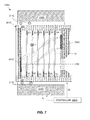
- FIG. 7 illustrates an exemplary reflective mode EB detector 200 C that utilizes a multi-pole magnetic deflector coil 211 C disposed between vacuum tube structure 201 C and permanent magnet 212 C, where multi-pole deflector coil 211 C is configured to generate a deflective magnetic field ⁇ right arrow over (B) ⁇ def (directed perpendicular to the drawing sheet) having sufficient strength to direct photoelectrons toward sensor 104 C.
- EB detector 200 C also includes a photocathode 101 C configured in a manner described above with reference to FIG. 5 , and ring electrodes E 1 to En that function as described above with reference to FIG. 2 .
- multi-pole deflector coils 211 C are inserted between vacuum tube structure 201 C and a solenoid.
- Deflector coil 211 C is positioned in a manner that generates an out-of-plane magnetic field, whereby photoelectrons leaving photocathode 101 C will be deflected upwards toward sensor 104 C.
- the magnetic solenoid in this design only needs to be slightly larger than the vacuum tube wrapped with deflector coils.
- the diameter of the magnetic pole piece in our design is significantly smaller. If the magnetic pole piece diameter is smaller, it requires less total magnetic flux to create the same magnetic field on the vacuum tube axis, which in turn can make magnetic solenoid even smaller.
- the design of the magnetic deflectors is widely known in the field of electron optics. Dipole, quadrupole, sextupole, octopole and other magnetic deflector designs can all be used here.
- FIG. 8 illustrates a simplified large deflection angle reflective mode EB detector 200 D according to another exemplary embodiment of the present invention.
- EB detector 200 D is utilized, for example, when larger deflection angle is required to provide enough space for camera electronics attached to the sensor.
- photoelectrons 805 are emitted from photocathode 101 D under photon illumination LLS, they will be immediately accelerated to a high voltage and focused by electron optics 802 .
- Electron optics 802 may include electrostatic lens and/or magnetic lens (e.g., utilizing ring electrodes E 1 to E 3 in the manner described above with reference to FIG. 4 ).
- a magnetic or electrostatic deflector or sector 803 is used to deflect the photoelectrons to a relatively large angle (e.g., 45° or more) away from the normal (optical) axis to the photocathode 104 D.
- a simple exemplary implementation of magnetic deflector 803 includes two permanent magnet plates with opposite polarity placed close to each other on opposite sides of the photoelectron path. A uniformly strong magnetic deflection field can be formed in the gap. Even though an exemplary deflection angle of 90° is shown in FIG. 8 , it is possible to deflect to other angles using the same design.
- Electrostatic and or magnetic lens can be used to form electron optics 806 (e.g., utilizing electrodes E 4 to En according to the embodiment described above with reference to FIG. 4 ). It is possible to have one or more than one intermediate conjugate planes along the path of the photoelectrons.
- FIG. 9A illustrates a surface inspection apparatus 900 that includes illumination system 901 and collection system 910 for inspecting areas of surface 911 .
- a laser system 915 is configured to direct light beam 902 through lens 903 .
- Lens 903 is oriented so that its principal plane is substantially parallel to surface 911 and, as a result, illumination line 905 is formed on surface 911 in the focal plane of lens 903 .
- light beam 902 and focused beam 904 are directed at a non-orthogonal angle of incidence to surface 911 .
- light beam 902 and focused beam 904 may be directed at an angle between about 1 degree and about 85 degrees from a normal direction to surface 911 .
- illumination line 905 is substantially in the plane of incidence of focused beam 904 .
- illumination line might be approximately 1 or 2, or a few, mm long and 1, 2 or a few ⁇ m wide.
- the illumination may be focused into a series of discrete spots.
- Collection system 910 includes lens 912 for collecting light scattered from illumination line 905 and lens 913 for focusing the light coming out of lens 912 onto a device, such as an EBCCD detector 914 including the above-described control device.
- a device such as an EBCCD detector 914 including the above-described control device.
- Dynamic adjustment of the gain of EBCCD detector 914 is important in this kind of inspection system because the scattered and diffracted light levels (and the efficiency of the filters) can vary dramatically from one region of a wafer to another due to the different patterns on the wafer.
- EBCCD detector 914 may include a linear array of detectors. In such cases, the linear array of detectors within EBCCD detector 914 can be oriented parallel to illumination line 915 . In one embodiment, multiple collection systems can be included, wherein each of the collection systems includes similar components, but differ in orientation.
- FIG. 9B illustrates an exemplary array of collection systems 921 , 922 , and 923 for a surface inspection apparatus (wherein its illumination system, e.g. similar to that of illumination system 901 , is not shown for simplicity).
- U.S. Pat. No. 7,525,649 which issued on Apr. 8, 2009 and is incorporated by reference herein, describes certain aspects of inspection system 901 in greater detail.
- FIG. 10 illustrates another dark-field wafer inspection system 1000 including a plurality of EBCCD/EBCMOS detectors.
- illumination optics 1002 receives the light beam(s) emitted by a light source 1001 .
- illumination optics 1002 may include multiple beam splitters and reflective optical elements that provide substantially parallel output light beams to a refractive optical element. That refractive optical element, in turn, can focus the multiple light beams onto a sample 1003 .
- optical collection subsystem 1007 may further include refractive optical elements 1005 that are configured to assist the other elements of optical collection subsystem 1007 in imaging the scattered light onto image detectors 1006 .
- at least one of image detectors 1006 can include the above-described EBCCD/EBCMOS detector.
- one detector may be optimized for substantial light scattering while another detector may be optimized for substantially low light scattering.
- the optical element may be configured to direct one portion of the scattered light to one image detector optimized for substantial light scattering and to direct another, different portion of the scattered light to a different image detector that is optimized for low-light scattering.
- U.S. Patent Pub. No. 2014/0009759 A1 issued to Guoheng Zhao et al. in 2014 describes dark field wafer inspection system 900 in more detail.
Priority Applications (7)
| Application Number | Priority Date | Filing Date | Title |
|---|---|---|---|
| US14/614,088 US9460886B2 (en) | 2014-07-22 | 2015-02-04 | High resolution high quantum efficiency electron bombarded CCD or CMOS imaging sensor |
| JP2017503495A JP6657175B2 (ja) | 2014-07-22 | 2015-07-15 | 高解像度且つ高量子効率の電子衝撃ccdまたはcmos撮像センサ |
| CN201580039421.8A CN106537596B (zh) | 2014-07-22 | 2015-07-15 | 用于检测低光信号的电子轰击检测器及其操作方法 |
| PCT/US2015/040618 WO2016014318A1 (en) | 2014-07-22 | 2015-07-15 | High resolution high quantum efficiency electron bombarded ccd or cmos imaging sensor |
| TW104123752A TWI646568B (zh) | 2014-07-22 | 2015-07-22 | 高解析度高量子效率之電子轟擊之電荷耦合裝置或互補金氧半導體成像感測器 |
| IL249255A IL249255B (en) | 2014-07-22 | 2016-11-28 | An electron bombarded ccd or cmos imaging sensor with high resolution and high quantum efficiency |
| JP2020018027A JP6826218B2 (ja) | 2014-07-22 | 2020-02-05 | 電子衝撃検出器を動作させる方法 |
Applications Claiming Priority (2)
| Application Number | Priority Date | Filing Date | Title |
|---|---|---|---|
| US201462027679P | 2014-07-22 | 2014-07-22 | |
| US14/614,088 US9460886B2 (en) | 2014-07-22 | 2015-02-04 | High resolution high quantum efficiency electron bombarded CCD or CMOS imaging sensor |
Publications (2)
| Publication Number | Publication Date |
|---|---|
| US20160027605A1 US20160027605A1 (en) | 2016-01-28 |
| US9460886B2 true US9460886B2 (en) | 2016-10-04 |
Family
ID=55163562
Family Applications (1)
| Application Number | Title | Priority Date | Filing Date |
|---|---|---|---|
| US14/614,088 Active 2035-04-24 US9460886B2 (en) | 2014-07-22 | 2015-02-04 | High resolution high quantum efficiency electron bombarded CCD or CMOS imaging sensor |
Country Status (6)
| Country | Link |
|---|---|
| US (1) | US9460886B2 (ja) |
| JP (2) | JP6657175B2 (ja) |
| CN (1) | CN106537596B (ja) |
| IL (1) | IL249255B (ja) |
| TW (1) | TWI646568B (ja) |
| WO (1) | WO2016014318A1 (ja) |
Cited By (1)
| Publication number | Priority date | Publication date | Assignee | Title |
|---|---|---|---|---|
| US20160299333A1 (en) * | 2015-04-09 | 2016-10-13 | Goodrich Corporation | Optical sensors |
Families Citing this family (4)
| Publication number | Priority date | Publication date | Assignee | Title |
|---|---|---|---|---|
| US10748739B2 (en) * | 2018-10-12 | 2020-08-18 | Kla-Tencor Corporation | Deflection array apparatus for multi-electron beam system |
| FR3096506B1 (fr) * | 2019-05-23 | 2021-06-11 | Photonis France | Photocathode à rendement quantique amélioré |
| CN110057293A (zh) * | 2019-05-31 | 2019-07-26 | 大理大学 | 电子落点位置检测装置 |
| CN112071732B (zh) * | 2020-07-28 | 2021-11-19 | 西安交通大学 | 一种可编码阵列式静电偏转器、聚焦偏转系统及设计方法 |
Citations (10)
| Publication number | Priority date | Publication date | Assignee | Title |
|---|---|---|---|---|
| US5321334A (en) | 1989-11-22 | 1994-06-14 | Hamamatsu Photonics K.K. | Imaging device |
| US5475227A (en) * | 1992-12-17 | 1995-12-12 | Intevac, Inc. | Hybrid photomultiplier tube with ion deflector |
| US6198221B1 (en) | 1996-07-16 | 2001-03-06 | Hamamatsu Photonics K.K. | Electron tube |
| US20010017344A1 (en) | 1999-07-20 | 2001-08-30 | Aebi Verle W. | Electron bombarded passive pixel sensor imaging |
| US6285018B1 (en) | 1999-07-20 | 2001-09-04 | Intevac, Inc. | Electron bombarded active pixel sensor |
| US20060054778A1 (en) | 2003-02-07 | 2006-03-16 | Klaus Suhling | Photon arrival time detection |
| US20130112856A1 (en) | 2010-05-14 | 2013-05-09 | The Regents Of The University Of California | Vacuum photosensor device with electron lensing |
| US20130148112A1 (en) | 2011-12-12 | 2013-06-13 | Kla-Tencor Corporation | Electron-Bombarded Charge-Coupled Device And Inspection Systems Using EBCCD Detectors |
| US20130264481A1 (en) | 2012-04-10 | 2013-10-10 | Kla-Tencor Corporation | Back-Illuminated Sensor With Boron Layer |
| US20140063502A1 (en) | 2012-08-28 | 2014-03-06 | Kla-Tencor Corporation | Image Intensifier Tube Design for Aberration Correction and Ion Damage Reduction |
Family Cites Families (4)
| Publication number | Priority date | Publication date | Assignee | Title |
|---|---|---|---|---|
| US6747258B2 (en) * | 2001-10-09 | 2004-06-08 | Itt Manufacturing Enterprises, Inc. | Intensified hybrid solid-state sensor with an insulating layer |
| US7283166B1 (en) * | 2002-10-15 | 2007-10-16 | Lockheed Martin Corporation | Automatic control method and system for electron bombarded charge coupled device (“EBCCD”) sensor |
| US7564544B2 (en) * | 2006-03-22 | 2009-07-21 | 3i Systems Corporation | Method and system for inspecting surfaces with improved light efficiency |
| CN102798735B (zh) * | 2012-08-14 | 2015-03-04 | 厦门大学 | 针尖增强暗场显微镜、电化学测试装置和调平系统 |
-
2015
- 2015-02-04 US US14/614,088 patent/US9460886B2/en active Active
- 2015-07-15 WO PCT/US2015/040618 patent/WO2016014318A1/en active Application Filing
- 2015-07-15 CN CN201580039421.8A patent/CN106537596B/zh active Active
- 2015-07-15 JP JP2017503495A patent/JP6657175B2/ja active Active
- 2015-07-22 TW TW104123752A patent/TWI646568B/zh active
-
2016
- 2016-11-28 IL IL249255A patent/IL249255B/en active IP Right Grant
-
2020
- 2020-02-05 JP JP2020018027A patent/JP6826218B2/ja active Active
Patent Citations (10)
| Publication number | Priority date | Publication date | Assignee | Title |
|---|---|---|---|---|
| US5321334A (en) | 1989-11-22 | 1994-06-14 | Hamamatsu Photonics K.K. | Imaging device |
| US5475227A (en) * | 1992-12-17 | 1995-12-12 | Intevac, Inc. | Hybrid photomultiplier tube with ion deflector |
| US6198221B1 (en) | 1996-07-16 | 2001-03-06 | Hamamatsu Photonics K.K. | Electron tube |
| US20010017344A1 (en) | 1999-07-20 | 2001-08-30 | Aebi Verle W. | Electron bombarded passive pixel sensor imaging |
| US6285018B1 (en) | 1999-07-20 | 2001-09-04 | Intevac, Inc. | Electron bombarded active pixel sensor |
| US20060054778A1 (en) | 2003-02-07 | 2006-03-16 | Klaus Suhling | Photon arrival time detection |
| US20130112856A1 (en) | 2010-05-14 | 2013-05-09 | The Regents Of The University Of California | Vacuum photosensor device with electron lensing |
| US20130148112A1 (en) | 2011-12-12 | 2013-06-13 | Kla-Tencor Corporation | Electron-Bombarded Charge-Coupled Device And Inspection Systems Using EBCCD Detectors |
| US20130264481A1 (en) | 2012-04-10 | 2013-10-10 | Kla-Tencor Corporation | Back-Illuminated Sensor With Boron Layer |
| US20140063502A1 (en) | 2012-08-28 | 2014-03-06 | Kla-Tencor Corporation | Image Intensifier Tube Design for Aberration Correction and Ion Damage Reduction |
Non-Patent Citations (4)
| Title |
|---|
| Buontempo, S,. "The Megapixel EBCCD: A high-resolution imaging tube sensitive to single photons", Nuclear Instruments & Methods In Physics Research A, Aug. 1998, pp. 255-262. |
| Grubisic, D., et al., "New Silicon Reach-Through Avalanche Photodiodes with Enhanced Sensitivity in the DUV/UV Wavelength Range", MIPRO 2013, May 20-24, 2013, Opatija, Croatia, pp. 48-54. |
| Ishigami, Yoshihiro et al.; "Development of a high-sensitivity UV photocathode using GaN film that works in transmission mode", Proceedings of SPIE vol. 8359 in 2012, 10 pages. |
| Opal, Chet B.; "Evaluation of large format electron bombarded virtual phase CCDs as ultraviolet imaging detectors", SPIE vol. 1158 Ultraviolet Technology III (1989), 8 pages. |
Cited By (2)
| Publication number | Priority date | Publication date | Assignee | Title |
|---|---|---|---|---|
| US20160299333A1 (en) * | 2015-04-09 | 2016-10-13 | Goodrich Corporation | Optical sensors |
| US9684162B2 (en) * | 2015-04-09 | 2017-06-20 | Goodrich Corporation | Optical sensors |
Also Published As
| Publication number | Publication date |
|---|---|
| IL249255B (en) | 2020-09-30 |
| TW201611072A (zh) | 2016-03-16 |
| JP2017531280A (ja) | 2017-10-19 |
| JP2020074331A (ja) | 2020-05-14 |
| CN106537596A (zh) | 2017-03-22 |
| TWI646568B (zh) | 2019-01-01 |
| JP6657175B2 (ja) | 2020-03-04 |
| CN106537596B (zh) | 2018-09-14 |
| US20160027605A1 (en) | 2016-01-28 |
| WO2016014318A1 (en) | 2016-01-28 |
| JP6826218B2 (ja) | 2021-02-03 |
| IL249255A0 (en) | 2017-02-28 |
Similar Documents
| Publication | Publication Date | Title |
|---|---|---|
| JP6826218B2 (ja) | 電子衝撃検出器を動作させる方法 | |
| KR102454320B1 (ko) | 복수의 하전 입자 빔들을 이용하여 샘플을 검사하는 장치 및 방법 | |
| US10236155B2 (en) | Detection assembly, system and method | |
| US6365897B1 (en) | Electron beam type inspection device and method of making same | |
| JP6880209B2 (ja) | 走査電子顕微鏡 | |
| US10903042B2 (en) | Apparatus and method for inspecting a sample using a plurality of charged particle beams | |
| US6633034B1 (en) | Method and apparatus for imaging a specimen using low profile electron detector for charged particle beam imaging apparatus including electrostatic mirrors | |
| JP2021048114A (ja) | 走査型電子顕微鏡および走査型電子顕微鏡の2次電子検出方法 | |
| JP3244620B2 (ja) | 走査電子顕微鏡 | |
| CN110709960B (zh) | 带电粒子束装置 | |
| JP2021068505A (ja) | 電子線装置及び電極 | |
| US7566873B1 (en) | High-resolution, low-distortion and high-efficiency optical coupling in detection system of electron beam apparatus | |
| USRE29500E (en) | Scanning charged beam particle beam microscope | |
| JP7474372B2 (ja) | 電子検出装置 | |
| JPH03295141A (ja) | 検出器 | |
| US9076629B2 (en) | Particle detection system | |
| WO2001084590A2 (en) | Method and apparatus for imaging a specimen using indirect in-column detection of secondary electrons in a microcolumn | |
| JP2014082008A (ja) | 撮像デバイス | |
| Carlini et al. | PROPOSAL FOR A PHOTON DETECTOR WITH PICOSECOND TIME RESOLUTION | |
| JP2006343346A (ja) | 基板検査方法および基板検査システム | |
| JP2007073529A (ja) | イメージインテンシファイア装置および方法 |
Legal Events
| Date | Code | Title | Description |
|---|---|---|---|
| AS | Assignment |
Owner name: KLA-TENCOR CORPORATION, CALIFORNIA Free format text: ASSIGNMENT OF ASSIGNORS INTEREST;ASSIGNORS:JIANG, XIMAN;BIELLAK, STEPHEN;FIELDEN, JOHN;REEL/FRAME:034893/0262 Effective date: 20150203 |
|
| STCF | Information on status: patent grant |
Free format text: PATENTED CASE |
|
| CC | Certificate of correction | ||
| MAFP | Maintenance fee payment |
Free format text: PAYMENT OF MAINTENANCE FEE, 4TH YEAR, LARGE ENTITY (ORIGINAL EVENT CODE: M1551); ENTITY STATUS OF PATENT OWNER: LARGE ENTITY Year of fee payment: 4 |
|
| MAFP | Maintenance fee payment |
Free format text: PAYMENT OF MAINTENANCE FEE, 8TH YEAR, LARGE ENTITY (ORIGINAL EVENT CODE: M1552); ENTITY STATUS OF PATENT OWNER: LARGE ENTITY Year of fee payment: 8 |