US9430960B2 - Display device and driving method thereof - Google Patents
Display device and driving method thereof Download PDFInfo
- Publication number
- US9430960B2 US9430960B2 US14/148,501 US201414148501A US9430960B2 US 9430960 B2 US9430960 B2 US 9430960B2 US 201414148501 A US201414148501 A US 201414148501A US 9430960 B2 US9430960 B2 US 9430960B2
- Authority
- US
- United States
- Prior art keywords
- image signal
- row
- input image
- coupling index
- data
- Prior art date
- Legal status (The legal status is an assumption and is not a legal conclusion. Google has not performed a legal analysis and makes no representation as to the accuracy of the status listed.)
- Active, expires
Links
- 238000000034 method Methods 0.000 title claims abstract description 29
- 230000008878 coupling Effects 0.000 claims abstract description 106
- 238000010168 coupling process Methods 0.000 claims abstract description 106
- 238000005859 coupling reaction Methods 0.000 claims abstract description 106
- 230000015654 memory Effects 0.000 claims abstract description 28
- 238000006243 chemical reaction Methods 0.000 claims description 24
- 230000006870 function Effects 0.000 claims description 9
- 238000010586 diagram Methods 0.000 description 22
- 238000005516 engineering process Methods 0.000 description 10
- 239000003086 colorant Substances 0.000 description 7
- 230000003111 delayed effect Effects 0.000 description 4
- 239000004973 liquid crystal related substance Substances 0.000 description 3
- 230000008569 process Effects 0.000 description 3
- 239000011159 matrix material Substances 0.000 description 2
- 230000000630 rising effect Effects 0.000 description 2
- 230000002123 temporal effect Effects 0.000 description 2
- 239000010409 thin film Substances 0.000 description 2
- 230000008901 benefit Effects 0.000 description 1
- 230000005540 biological transmission Effects 0.000 description 1
- 238000004364 calculation method Methods 0.000 description 1
- 230000015556 catabolic process Effects 0.000 description 1
- 239000000470 constituent Substances 0.000 description 1
- 230000003247 decreasing effect Effects 0.000 description 1
- 238000006731 degradation reaction Methods 0.000 description 1
- 230000000694 effects Effects 0.000 description 1
- 230000002708 enhancing effect Effects 0.000 description 1
- 238000012986 modification Methods 0.000 description 1
- 230000004048 modification Effects 0.000 description 1
Images


Classifications
-
- G—PHYSICS
- G09—EDUCATION; CRYPTOGRAPHY; DISPLAY; ADVERTISING; SEALS
- G09G—ARRANGEMENTS OR CIRCUITS FOR CONTROL OF INDICATING DEVICES USING STATIC MEANS TO PRESENT VARIABLE INFORMATION
- G09G3/00—Control arrangements or circuits, of interest only in connection with visual indicators other than cathode-ray tubes
- G09G3/20—Control arrangements or circuits, of interest only in connection with visual indicators other than cathode-ray tubes for presentation of an assembly of a number of characters, e.g. a page, by composing the assembly by combination of individual elements arranged in a matrix no fixed position being assigned to or needed to be assigned to the individual characters or partial characters
- G09G3/34—Control arrangements or circuits, of interest only in connection with visual indicators other than cathode-ray tubes for presentation of an assembly of a number of characters, e.g. a page, by composing the assembly by combination of individual elements arranged in a matrix no fixed position being assigned to or needed to be assigned to the individual characters or partial characters by control of light from an independent source
- G09G3/36—Control arrangements or circuits, of interest only in connection with visual indicators other than cathode-ray tubes for presentation of an assembly of a number of characters, e.g. a page, by composing the assembly by combination of individual elements arranged in a matrix no fixed position being assigned to or needed to be assigned to the individual characters or partial characters by control of light from an independent source using liquid crystals
- G09G3/3611—Control of matrices with row and column drivers
- G09G3/3614—Control of polarity reversal in general
-
- G—PHYSICS
- G09—EDUCATION; CRYPTOGRAPHY; DISPLAY; ADVERTISING; SEALS
- G09G—ARRANGEMENTS OR CIRCUITS FOR CONTROL OF INDICATING DEVICES USING STATIC MEANS TO PRESENT VARIABLE INFORMATION
- G09G2320/00—Control of display operating conditions
- G09G2320/02—Improving the quality of display appearance
- G09G2320/0209—Crosstalk reduction, i.e. to reduce direct or indirect influences of signals directed to a certain pixel of the displayed image on other pixels of said image, inclusive of influences affecting pixels in different frames or fields or sub-images which constitute a same image, e.g. left and right images of a stereoscopic display
-
- G—PHYSICS
- G09—EDUCATION; CRYPTOGRAPHY; DISPLAY; ADVERTISING; SEALS
- G09G—ARRANGEMENTS OR CIRCUITS FOR CONTROL OF INDICATING DEVICES USING STATIC MEANS TO PRESENT VARIABLE INFORMATION
- G09G2320/00—Control of display operating conditions
- G09G2320/02—Improving the quality of display appearance
- G09G2320/0219—Reducing feedthrough effects in active matrix panels, i.e. voltage changes on the scan electrode influencing the pixel voltage due to capacitive coupling
-
- G—PHYSICS
- G09—EDUCATION; CRYPTOGRAPHY; DISPLAY; ADVERTISING; SEALS
- G09G—ARRANGEMENTS OR CIRCUITS FOR CONTROL OF INDICATING DEVICES USING STATIC MEANS TO PRESENT VARIABLE INFORMATION
- G09G2320/00—Control of display operating conditions
- G09G2320/02—Improving the quality of display appearance
- G09G2320/0223—Compensation for problems related to R-C delay and attenuation in electrodes of matrix panels, e.g. in gate electrodes or on-substrate video signal electrodes
-
- G—PHYSICS
- G09—EDUCATION; CRYPTOGRAPHY; DISPLAY; ADVERTISING; SEALS
- G09G—ARRANGEMENTS OR CIRCUITS FOR CONTROL OF INDICATING DEVICES USING STATIC MEANS TO PRESENT VARIABLE INFORMATION
- G09G2320/00—Control of display operating conditions
- G09G2320/02—Improving the quality of display appearance
- G09G2320/0233—Improving the luminance or brightness uniformity across the screen
-
- G—PHYSICS
- G09—EDUCATION; CRYPTOGRAPHY; DISPLAY; ADVERTISING; SEALS
- G09G—ARRANGEMENTS OR CIRCUITS FOR CONTROL OF INDICATING DEVICES USING STATIC MEANS TO PRESENT VARIABLE INFORMATION
- G09G2320/00—Control of display operating conditions
- G09G2320/02—Improving the quality of display appearance
- G09G2320/0257—Reduction of after-image effects
-
- G—PHYSICS
- G09—EDUCATION; CRYPTOGRAPHY; DISPLAY; ADVERTISING; SEALS
- G09G—ARRANGEMENTS OR CIRCUITS FOR CONTROL OF INDICATING DEVICES USING STATIC MEANS TO PRESENT VARIABLE INFORMATION
- G09G2320/00—Control of display operating conditions
- G09G2320/02—Improving the quality of display appearance
- G09G2320/0285—Improving the quality of display appearance using tables for spatial correction of display data
Definitions
- the described technology generally relates to a display device and a driving method thereof.
- Display devices such as liquid crystal displays (LCDs) and organic light-emitting diode (OLED) displays, generally include a display panel and a driving device for driving the display panel.
- LCDs liquid crystal displays
- OLED organic light-emitting diode
- the display panel generally includes a plurality of signal lines and a plurality of pixels PX which are connected to the signal lines and are arranged in a substantially matrix form.
- the signal lines generally include a plurality of gate lines transferring gate signals and a plurality of data lines transferring data voltages.
- Each pixel generally includes at least one switching element connected to a corresponding gate line and a corresponding data line, at least one pixel electrode connected to the switching element, and a counter electrode which faces the pixel electrode and is applied with a common voltage.
- the switching element generally includes at least one thin film transistor and is turned on or turned off depending on the gate signal transferred by the gate line to selectively transfer the data voltage transferred by the data line to the pixel electrode.
- Each pixel typically displays an image with a luminance depending on the difference between the data voltage and the common voltage.
- Images displayed on a display device are generally divided into still images and moving images.
- a still image can be displayed and when the image signals of adjacent frames are different from each other, a moving image can be displayed.
- the driving device generally includes a graphic processing unit (GPU), a driver, and a signal controller which controls the driver.
- the graphic processing unit transfers an input image signal for the image to be displayed on the display panel to the signal controller and the signal controller generates a control signal for driving the display panel and transfers the generated control signal to the driver, along with the image signal.
- the driver generally includes a gate driver which generates the gate signals and a data driver which generates the data voltages.
- One inventive aspect is a display device for enhancing a display quality by removing a ghost phenomenon or a shading phenomenon which is caused by charging-type coupling of all the adjacent rows.
- One inventive aspect is a display device including a display panel including a plurality of pixels, a data driver transferring data voltages to a plurality of data lines, a gate driver transferring gate signals to a plurality of gate lines, and a signal controller controlling the data driver and the gate driver and including a signal processor, in which the signal processor includes a memory storing an input image signal of an (N ⁇ 1)-th (N is a natural number of 2 or more) row and an input image signal of an N-th row, and a coupling index calculator calculating a coupling index which represents a degree of coupling between adjacent rows, and the signal processor compensates for the input image signal of a pixel of the N-th row to generate a compensated image single by using an input image signal of an (N+1)-th row, the input image signal of the (N ⁇ 1)-th row and the input image signal of the N-th row which are received from the memory, and the calculated coupling index.
- the signal processor includes a memory storing an input image signal of an (N ⁇
- the coupling index may depend on a function which depends on the characteristics of the display panel.
- the signal processor may further include a three-dimensional lookup table unit which includes a plurality of lookup tables each storing compensation values according to the coupling index.
- the three-dimensional lookup table unit may include a lookup table which corresponds to a positive coupling index and stores compensation values depending on values of the input image signal of the (N ⁇ 1)-th row and the input image signal of the N-th row and a lookup table which corresponds to a negative coupling index and stores compensation values depending on values of the input image signal of the (N+1)-th row and the input image signal of the N-th row.
- the signal processor may further include a signal compensator which generates a compensated image signal by using the compensation values received from the three-dimensional lookup table unit.
- the signal processor may include a GV converter (or a gray-to-voltage converter) converting the input image signal of the (N ⁇ 1)-th row, the input image signal of the N-th row, and the input image signal of the (N+1)-th row into voltages, a compensation voltage generator generating a compensation voltage by using the converted voltages from the GV converter and the coupling index, and a VG converter converting the compensation voltage into a gray.
- a GV converter or a gray-to-voltage converter
- the GV converter may include a conversion lookup table which is defined depending on a function between the data voltage applied to the display panel and grays.
- the VG converter (or a voltage-to-gray converter) may convert the compensation voltage into the gray by using the conversion lookup table.
- Another aspect is a method of driving a display device including a display panel, a data driver, a gate driver, and a signal controller, the method including storing an input image signal of an (N ⁇ 1)-th (N is a natural number of 2 or more) row and an input image signal of an N-th row, calculating a coupling index which represents a degree of coupling between adjacent rows, and compensating for the input image signal of a pixel of the N-th row by using an input image signal of the (N+1)-th row, the input image signal of the (N ⁇ 1)-th row and the input image signal of the N-th row, and the calculated coupling index to generate a compensated image signal for one pixel of the N-th row.
- the calculating of the coupling index may include using a distance from the data driver to the pixel and a distance from the gate driver to the pixel.
- the calculating of the coupling index may include tuning the coupling index by using a one-dimensional function according to characteristics of the display panel.
- the compensating of the input image signal for the pixel of the N-th row may include using a three-dimensional lookup table unit which includes a plurality of lookup tables storing compensation values depending on the coupling index.
- the three-dimensional lookup table unit may include a lookup table which corresponds to a positive coupling index and stores compensation values depending on values of the input image signal of the (N ⁇ 1)-th row and the input image signal of the N-th row and a lookup table which corresponds to a negative coupling index and stores compensation values depending on values of the input image signal of the (N+1)-th row and the input image signal of the N-th row.
- the compensating of the input image signal for the pixel of the N-th row may include using the compensation values received from the three-dimensional lookup table unit.
- the compensating of the input image signal of the N-th row may include converting the input image signal of the (N ⁇ 1)-th row, the input image signal of the N-th row, and the input image signal of the (N+1)-th row into voltages, generating a compensation voltage by, using the converted voltage and the coupling index, and converting the compensation voltage into a gray.
- the converting of the input image signal of the (N ⁇ 1)-th, the input image signal of the N-th row, and the input image signal of the (N+1)-th row into the voltages may include using a conversion lookup table which is defined depending on a functional relationship between the data voltage applied to the display panel and grays.
- the converting of the compensation voltage into the gray may include using the conversion lookup table.
- the described technology it is possible to enhance the display quality of a display device by substantially removing a ghosting phenomenon or a shading phenomenon which is caused by charging-type coupling of the display device.
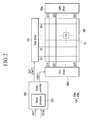
- FIGS. 1 and 2 are block diagrams of a display device according to an exemplary embodiment of the described technology.
- FIG. 3 is a block diagram of a signal compensator of the display device according to an exemplary embodiment.
- FIG. 4 is a diagram illustrating a three-dimensionally configured lookup table included in a signal controller of the display device according to an exemplary embodiment.
- FIGS. 5 and 6 are diagrams illustrating one lookup table included in a three-dimensionally configured lookup table included in the signal controller of the display device according to an exemplary embodiment.
- FIGS. 7 and 8 are timing diagrams of driving signals of the display device according to an exemplary embodiment.
- FIGS. 9 and 10 are block diagrams of the display device according to an exemplary embodiment.
- FIG. 11 is a block diagram of the display device according to an exemplary embodiment.
- FIG. 12 is a layout diagram of a pixel and a signal line of the display device according to an exemplary embodiment.
- FIG. 13 is a block diagram illustrating an example of positions at which color blurring may appear when the display device according to an exemplary embodiment displays an image having a predetermined gray.
- FIG. 14 is a block diagram of a signal compensator of the display device according to an exemplary embodiment.
- FIG. 15 is a diagram illustrating a lookup table included in a GV converter and a VG converter as illustrated in FIG. 14 .
- FIG. 16 is a flow chart illustrating a method of compensating for an input image signal in the display device according to an exemplary embodiment.
- shading may occur in which a data voltage of the following row is applied to the current row due to signal delay.
- FIGS. 1 and 2 are block diagrams of a display device according to an exemplary embodiment and FIG. 3 is a block diagram of a signal compensator of the display device according to an exemplary embodiment.
- FIG. 4 is a diagram illustrating a three-dimensionally configured lookup table included in a signal controller of the display device according to an exemplary embodiment and
- FIGS. 5 and 6 are diagrams illustrating one lookup table included in the three-dimensionally configured lookup table according to an exemplary embodiment.
- the display device includes a display panel 300 , a gate driver 400 , a data driver 500 , and a signal controller 600 which controls the data driver 500 and the gate driver 400 .
- the display panel 300 may be a display panel which is included in various flat panel displays (FPDs), such as a liquid crystal display (LCD), an organic light-emitting diode (OLED) display, or an electrowetting display (EWD).
- FPDs flat panel displays
- LCD liquid crystal display
- OLED organic light-emitting diode
- EWD electrowetting display
- the display panel 300 includes a plurality of gate lines G 1 to Gn, a plurality of data lines D 1 to Dm, and a plurality of pixels PXs which are connected to the gate lines G 1 to Gn and the data lines D 1 to Dm.
- the gate lines G 1 to Gn may transfer gate signals, and may extend in a substantially row direction and be substantially parallel to each other.
- the data lines D 1 to Dm may transfer data voltages, and may extend in a substantially column direction and be substantially parallel to each other.
- the pixels PXs may be arranged in a substantially matrix form.
- Each pixel PX may include at least one switching element connected to the corresponding gate lines G 1 to Gn and the corresponding data lines D 1 to Dm and at least one pixel electrode connected to the switching element.
- the switching element may include at least one thin film transistor and is turned on or turned off depending on the gate signals transferred by the gate lines G 1 to Gn to selectively transfer the data voltage transferred by the data lines D 1 to Dm to the pixel electrode.
- Each pixel PX may display an image with a luminance depending on the data voltage applied to the pixel electrode.
- Each pixel PX displays one of primary colors (spatial division) or each pixel PX alternately displays the primary colors over time (temporal division), such that desired colors may be recognized by the spatial and temporal sum of the displayed primary colors.
- An example of the primary colors may include three primary colors, such as red, green, and blue.
- a plurality of adjacent pixels PX displaying different primary colors may together form one set (referred to as a dot). The dot may display a white image.
- the gate driver 400 receives a gate control signal CONT 1 from the signal controller 600 and generates gate signals which are a combination of a gate-on voltage Von and a gate-off voltage Voff capable of turning on and turning off the switching elements of the pixels PX based on the transferred gate control signal CONT 1 .
- the gate control signal CONT 1 includes a scanning start signal STV which instructs a scanning start and at least one clock signal CPV which controls an output period of the gate-on voltage Von, and the like.
- the gate driver 400 is connected to the gate lines G 1 to Gn of the display panel 300 to apply the gate signals to the gate lines G 1 to Gn.
- the gate driver 400 may include first and second gate drivers 400 a and 400 b which are disposed at both sides of the display panel 300 .
- the gate lines G 1 to Gn may be divided into first gate lines G 11 to Gn 1 and second gate lines G 12 to Gn 2 which are disposed in different regions of the display panel.
- the first gate lines G 11 to Gn 1 are connected to the first gate driver 400 a to receive the gate signals and the second gate lines G 12 to Gn 2 are connected to the second gate driver 400 b to receive the gate signals.
- the data driver 500 receives a data control signal CONT 2 and output image signals DAT from the signal controller 600 .
- the data driver 500 selects a gray voltage corresponding to each output image signal DAT, thereby converting the output image signal DAT into a data voltage which is an analog data signal.
- the output image signal DAT which is a digital signal, has a defined number of values (or grays).
- the data control signal CONT 2 includes a horizontal synchronization start signal which indicates a transmission start of the output image signal DAT of a pixel PX of one row, at least one data load signal TP and a data clock signal which represents an instruction to apply the data voltage to the data lines D 1 to Dm, and the like.
- the data control signal CONT 2 may further include an inversion signal that inverts the polarity of the data voltage with respect to a common voltage Vcom (referred to as the polarity of the data voltage).
- the data driver 500 is connected to the data lines D 1 to Dm of the display panel 300 to apply data voltages Vd to the corresponding data lines D 1 to Dm.
- the data driver 500 may also include a pair of data drivers (not illustrated) which face each other at upper and lower portions of the display panel 300 .
- the data driver disposed at the upper portion may apply the data voltages Vd from above the data lines D 1 to Dm of the display panel 300 and the data driver disposed at the lower portion may apply the data voltages Vd from under the data lines D 1 to Dm of the display panel 300 .
- the data lines D 1 to Dm connected to the data driver disposed at the lower portion and the data lines D 1 to Dm connected to the data driver disposed at the upper portion may also be separated from each other.
- the signal controller 600 receives an input image signal IDAT and an input control signal ICON which controls the display thereof, from an external graphic processing unit (not illustrated) (or graphic processor), and the like.
- the signal controller 600 appropriately processes the input image signal IDAT based on the input control signal (ICON) to convert the input image signal IDAT into the output image signal DAT.
- the signal controller 600 generates the gate control signal CONT 1 , the data control signal CONT 2 , and the like, based on the input image signal IDAT and the input control signal ICON.
- the signal controller 600 transfers the gate control signal CONT 1 to the gate driver 400 and the data control signal CONT 2 and the processed output image signal DAT to the data driver 500 .
- the signal controller 600 includes a signal processor 650 which compensates for the input image signal IDAT.
- the signal processor 650 may include a memory 651 , a coupling index CX calculator 652 , a three-dimensional lookup table unit (LUT_3D) (or three-dimensional lookup table memory) 653 , and a signal compensator 654 .
- a memory 651 may include a memory 651 , a coupling index CX calculator 652 , a three-dimensional lookup table unit (LUT_3D) (or three-dimensional lookup table memory) 653 , and a signal compensator 654 .
- LUT_3D three-dimensional lookup table unit
- the memory 651 may include at least two line memories which may store the input image signals IDATs for each row.
- a current pixel row, used to compensate for the input image signal IDAT is set to be an N-th (N is a natural number) row
- the memory 651 may store the data of an input image signal IDAT of an (N ⁇ 1)-th row which is a previous row and the data of an input image signal IDAT of the N-th row.
- the memory 651 may transfer the stored data of the input image signal IDAT of the (N ⁇ 1)-th row and the stored data of the input image signal IDAT of the N-th row to the three-dimensional lookup table unit 653 .
- the coupling index CX calculator 652 stores or calculates the coupling index CX which represents the degree of charging-type coupling between the adjacent rows. At the time of calculating the coupling index CX, the coupling index CX may be calculated by using an interpolation method.
- the coupling index CX may vary depending on delay occurrence factors of the data voltages and the gate signals.
- the coupling index CX may depend on the degree of charging-type coupling based on the position of the pixels PX within the display panel 300 and the structure of the display panel 300 .
- the coupling index CX may be determined by displaying a reference pattern on the display and then measuring the actual degree of coupling.
- the coupling index CX may be a negative number, a positive number, or 0.
- the coupling index CX calculator 652 may transfer the calculated coupling index CX to the three-dimensional lookup table unit 653 .
- the three-dimensional lookup table unit 653 includes a plurality of different lookup tables depending on the coupling index CX. Each lookup table is configured two dimensionally, and the lookup tables are arranged depending on the coupling index CX such that the lookup table unit 653 is configured three dimensionally.
- Each lookup table of the three-dimensional lookup table unit 653 stores compensation values for some grays or all the grays of the input image signal IDAT of the N-th row.
- the three-dimensional lookup table unit 653 includes a ghost lookup table LUT_P corresponding to a positive coupling index CX and a shading lookup table LUT_N corresponding to a negative coupling index CX.
- the ghost lookup table LUT_P stores the compensation values of the input image signal IDAT of the N-th row for the gray of the input image signal IDAT of the (N ⁇ 1)-th row which is a previous row.
- the shading lookup table LUT_N stores the compensation value of the input image signal IDAT of the N-th row for the gray of the input image signal IDAT of the (N+1)-th row which is the following row.
- the compensation value of the input image signal IDAT of the N-th row in the corresponding lookup table may be the same as that of the original input image signal IDAT.
- the compensation value for grays which are not stored in each lookup table LUT_P and LUT_N may be obtained by a calculation method, such as various interpolation methods.
- the lookup tables for the coupling indices CX in which the lookup tables LUT_P and LUT_N are not prepared may be calculated by various interpolation methods using the compensation values of the adjacent lookup tables LUT_P and LUT_N.
- the three-dimensional lookup table unit 653 receives the coupling index CX from the coupling index calculator 652 , receives the data of the input image signal IDAT of the (N ⁇ 1)-th row and the data of the input image signal IDAT of the N-th row from the memory 651 , and receives the data of the input image signal IDAT of the (N+1)-th row input from a source external to the signal controller 600 to obtain the compensation values for the input image signals IDAT of the corresponding pixels PX from the lookup tables LUT_P and LUT_N.
- the three-dimensional lookup table unit 653 may transfer the compensation value for the input image signal IDAT of the pixel PX of the N-th row to the signal compensator 654 .
- the signal compensation unit 654 may compensate for and process the input image signal IDAT of the pixels PX of the N-th row by using the compensation value received from the three-dimensional lookup table unit 653 to generate the output image signal DAT.
- the output image signal DAT obtained by processing the compensated input image signal IDAT is input to the data driver 500 and the data driver 500 converts the output image signal DAT to generate the data voltages and output the generated data voltages to the display panel 300 .
- the three-dimensional lookup table unit 653 includes a plurality of lookup tables LUT_P and LUT_N depending on the coupling indices CX which relies on the position of the charged pixel PX within the display panel 300 and the degree of coupling for each position.
- the compensation values of each lookup table LUT_P and LUT_N vary depending on the difference in the data between the input image signals IDAT of the adjacent rows.
- the charging-type coupling between the adjacent rows due to the signal delay depending on the position of pixels PX of the display panel 300 may be substantially removed and the degradation in image quality, such as the charging-type blurring caused by the insufficient charging rate of the corresponding pixels PX, may be substantially prevented.
- FIGS. 7 and 8 are timing diagrams of driving signals of the display device according to an exemplary embodiment and FIGS. 9 and 10 are block diagrams of the display device according to an exemplary embodiment.
- the signal controller 600 receives the input image signal IDAT and the input control signal ICON from an external source and then generates and processes the compensated input image signal to convert the input image signal IDAT into the output image signal DAT.
- the controller also generates the gate control signal CONT 1 , the data control signal CONT 2 , and the like.
- the signal controller 600 transmits the gate control signal CONT 1 to the gate driver 400 and the data control signal CONT 2 and the output image signal DAT to the data driver 500 .
- the data driver 500 receives the output image signal DAT for the pixels PX of one row and receives the data control signal CONT 2 from the signal controller 600 . Depending on the data control signal CONT 2 , the data driver 500 selects the gray voltage corresponding to each output image signal DAT to convert the output image signal DAT into the data voltages Vd which are the analog data signal and then applies the data voltages Vd to the corresponding data lines D 1 to Dm.
- the gate driver 400 applies the gate-on voltage Von to the gate lines G 1 to Gn depending on the gate control signal CONT 1 received from the signal controller 600 to turn-on the switching elements connected to the gate lines G 1 to Gn.
- the data voltages Vd applied to the data lines D 1 to Dm are applied to the corresponding pixels PX through the turned on switching elements.
- the switching elements connected to the gate lines G 1 to Gn are turned on and the data voltages Vd applied to the data lines D 1 to Dm are applied to the corresponding pixels PX through the turned on switching elements.
- the data driver 500 synchronizes with a rising edge of the data load signal TP to sequentially apply the data voltages Vd to the data lines D 1 to Dm.
- the interval between adjacent rising edges of the data load signal TP may be a 1 horizontal period (written as “1H”, substantially the same as one period of a horizontal synchronizing signal Hsync and a data enable signal DE).
- FIG. 7 illustrates only a data voltage Vd(N ⁇ 1) of the (N ⁇ 1)-th row which is white and a data voltage Vd(N) of the N-th row which is black. Further, FIG. 7 illustrates only a gate signal Vg(N) which is applied to the N-th row.
- the data voltage Vd(N ⁇ 1) is delayed depending on the degree to which the pixel PX is spaced apart from the data driver 500 , and thus may be a delayed data voltage Vd(N ⁇ 1)_del.
- the delayed data voltage Vd(N ⁇ 1)_del may affect the charging time of the data voltage Vd(N) of the N-th row over most of the delay time Tdel. Therefore, the actual charging time Tdm in which the data voltage Vd(N) may be charged in the pixel PX of the N-th row may be reduced by a length of time obtained by subtracting the Tdel from 1H. Therefore, the charging time of the data voltage Vd(N) of the N-th row may be insufficient and the image of the pixel PX of the N-th row may be the grey image gray, not the target black image, resulting in a ghosting phenomenon.
- the ghosting phenomenon may occur in pixels PX which are far away from the data driver 500 and are at a position at which a small delay of the gate signal Vg(N) generated.
- the ghosting phenomenon corresponds to the case in which the coupling index CX is a positive number.
- the signal processor 650 uses the three-dimensional lookup table unit 653 to compensate for the input image signal IDAT of the N-th row and output a compensated data voltage Vd(N)′, such that the targeted black as indicated by the arrow in FIG. 7 may be displayed and the ghosting phenomenon may be substantially prevented.
- FIG. 8 illustrates the data voltage Vd(N) of the N-th row which is white and the data voltage Vd(N+1) of the (N+1)-th row which is black. Further, FIG. 8 illustrates only the gate signal Vg(N) which is applied to the N-th row.
- the gate signal Vg(N) is delayed depending on the distance from the pixel PX to the gate driver 400 .
- the gate signal Vg(N) is applied as a voltage larger than the gate-off voltage Voff to the gate lines G 1 to Gn until the end of the delay time Tgel of the charging time of the data voltage Vd(N+1) of the (N+1)-th row. Therefore, the pixels PX of the N-th row are further applied with the data voltage Vd(N+1) for the pixels PX of the (N+1)-th row, such that a shading phenomenon which causes the image of the corresponding pixels PX to deviate from the targeted luminance may occur.
- the shading phenomenon may occur in the pixels PX which are far away from the gate driver 400 and are at a position at which a small delay of the data voltage Vd is generated.
- the shading phenomenon corresponds to the case in which the coupling index CX is a negative number.
- the signal processor 650 uses the three-dimensional lookup table unit 653 to compensate for the input image signal IDAT of the N-th row and outputs the compensated data voltage Vd(N)′, such that the shading phenomenon may be substantially prevented.
- the image of one frame may be displayed by applying the gate-on voltage Von to all the gate lines G 1 to Gn and applying the data signal to the all the pixels PXs.
- a next frame starts after one frame ends and the state of the inversion signal applied to the data driver 500 is controlled so that the polarity of the data voltage Vd applied to each pixel PX is opposite to the polarity in the previous frame.
- the polarity of the data voltage Vd flowing through one of the data lines D 1 to Dm may be periodically changed or the polarities of the data voltages Vd applied to pixel rows may also be different from each other, even within one frame, depending on the characteristics of the inversion signal.
- the memory 651 included in the signal processor 650 may include a frame memory, instead of a line memory.
- the input image signal IDAT of the (N+1)-th row when referring to the data of the input image signal IDAT of the (N+1)-th row, which is the next row, the input image signal IDAT of the (N+1)-th row may also be changed by the data of the input image signal IDAT of the (N+2)-th row. Therefore, in order to compensate for the input image signal IDAT of the N-th row which is the current row, by referring to only the input image signal IDAT of the (N+1)-th row, the charging-type coupling compensation may not be complete. Therefore, the shading phenomenon may be substantially completely removed by compensating for the input image signal IDAT of the N-th row by referring to the input image signal IDAT of all of the subsequent rows through the frame memory of the memory 651 .
- FIG. 11 is a block diagram of the display device according to an exemplary embodiment
- FIG. 12 is a layout diagram of a pixel and a signal line of the display device according to an exemplary embodiment
- FIG. 13 is a block diagram illustrating an example of positions at which color blurring appears when the display device according to an exemplary embodiment displays an image having a predetermined gray.
- the coupling index CX may vary depending on the distance from each of the data driver 500 and the gate driver 400 to the corresponding pixel PX. Further, the degree of signal delay may vary depending on the structure of the display panel 300 and therefore the coupling index CX needs to be finely tuned to the individual characteristics of the display panel 300 .
- the coupling index CX may be calculated based on, for example, the following Equation 1.
- Cdx Ldx ⁇ ( Dn )
- Cgx Lgx ⁇ ( Gn )
- CX Cdx ⁇ Cgx Equation 1
- Ldx is a variable which represents the distance to the charged corresponding pixel PX from the data driver 500 and may be represented by (the row number of the pixel PX from the data driver 500 )/(the total number of rows). Therefore, Ldx may have a value which is larger than 0 and equal to or less than 1.
- Lgx is which is a variable representing the distance to the charged corresponding pixel PX from the gate driver 400 and may be represented by (the column number of the pixel from the gate driver 400 )/(the total number of columns through which the gate driver 400 transfers gate signals). Therefore, Lgx may have a value which is larger than 0 and equal to or smaller than 1.
- ⁇ (Dn) and ⁇ (Gn) are functions which tune the coupling index CX so as to meet the characteristics of the display panel 300 , in which Dn may represent the row number of the pixel PX from the data driver 500 and Gn may represent the column number of the pixel PX from the gate driver 400 .
- ⁇ (Dn) and ⁇ (Gn) may each be one-dimensional functions.
- ⁇ (Dn) and ⁇ (Gn) for tuning the coupling index CX may vary depending on the characteristics of the display panel 300 .
- a reference pattern may be displayed on the display panel 300 and the color uniformity generated by the charging-type coupling may be measured.
- the structure of the display panel 300 will be described with reference to FIG. 12 .
- the display panel 300 of the display device may include a plurality of gate lines Gi, G(i+1), . . . , which extend in a row direction, a plurality of data lines Dj, D(j+1), . . . , which extend in a column direction, and a plurality of pixels PXs.
- Each pixel PX may include a pixel electrode 191 which is connected to the gate lines Gi, G(i+1), . . . , and the data lines Dj, D(j+1), . . . , through the switching element Q.
- each pixel PX represents a primary color of red (R), green (G), or blue (B), but is not limited thereto.
- the pixels which represent the same primary color R, G, and B may be disposed in one pixel array.
- a pixel column of red pixels R, a pixel column of green pixels G, and a pixel column of blue pixels B may be alternately disposed.
- the data lines Dj, D(j+1), . . . may be each disposed in each pixel array and the gate lines G 1 , G(i+1), . . . may each be disposed in each pixel row, but the above exemplary embodiments are not limited thereto.
- the pixels R, G, and B which are disposed in one pixel array to represent the same primary color may be connected to any one of two data lines Dj, D(j+1), . . . , which are adjacent to each other.
- the pixels R, G, and B which are disposed in one pixel array may be alternately connected to two data lines Dj, D(j+1), . . . , which are adjacent to each other.
- the pixels R, G, and B which are disposed in the same pixel row may be connected to the same gate line Gi, Gi+1, . . . .
- the adjacent data lines Dj, D(j+1), . . . may be applied with data voltages which have opposite polarities to each other.
- the data voltages may have polarities which are inverted in each frame.
- the pixels R, G, and B which are adjacent to each other in a column direction may be applied with the data voltages having opposite polarities to each other and the pixels R, G, and B which are adjacent to each other in one pixel row may be applied with data voltages having opposite polarities to each other, such that the pixels R, G, and B may be driven in a substantially 1 ⁇ 1 dot inversion form. That is, even though the pixels R, G, and B are driven in a column inversion form in which the data voltages which are applied to the data lines Dj, D(j+1), . . . , maintain the same polarity for one frame, dot inversion driving may be realized.
- FIG. 13 illustrates positions at which the ghosting phenomenon may occur when a red gray of the reference pattern is 195, a green gray thereof is 25, and a blue gray thereof is 25.
- the green pixels G are affected by the data voltage of the red pixels R of the previous row and thus may become more greenish.
- the blue pixels B are affected by the data voltage of the red pixels R of the next row and thus may become more bluish.
- ⁇ (Dn) and ⁇ (Gn) may be defined based on the results obtained by the display characteristics of the color uniformity or the color blurring after the image of the reference pattern is displayed, and the coupling index CX may be tuned based on the defined ⁇ (Dn) and ⁇ (Gn).
- FIG. 14 is a block diagram of a signal compensator of the display device according to an exemplary embodiment
- FIG. 15 is a diagram illustrating a lookup table included in a GV converter and a VG converter illustrated in FIG. 14
- FIG. 16 is a flow chart illustrating a method of compensating for an input image signal in the display device according to an exemplary embodiment.
- the signal processor 650 may include a memory 651 , a GV converter 655 , a compensation voltage generator 656 , a coupling index CX calculator 652 , and a VG converter 657 .
- the memory 651 may transfer the stored data of the input image signal IDAT of the (N ⁇ 1)-th row and the stored data of the input image signal IDAT of the N-th row to the GV converter 655 .
- the GV converter 655 receives the data of the input image signal IDAT of the (N ⁇ 1)-th row and the data of the input image signal IDAT of the N-th row from the memory 651 , receives the data of the input image signal IDAT of the (N+1)-th row input from a source external to the signal controller 600 , and converts the gray G of the data into a voltage V. This is briefly referred to as a GV conversion.
- the GV converter 655 may include a conversion lookup table.
- the conversion lookup table is a one-dimensional lookup table and may be defined depending on a function between the data voltage applied to the display panel 300 and the gray.
- the function between the data voltage and the gray may vary depending on the characteristics of the display panel 300 , for example, depending on a voltage-luminance graph (VT curve) or a gamma characteristic of a liquid crystal in the case of an LCD.
- VT curve voltage-luminance graph
- gamma characteristic of a liquid crystal in the case of an LCD a voltage-luminance graph
- FIG. 15 illustrates an example of the conversion lookup table which is included in the GV converter 655 .
- the data voltage for each gray may be stored one-dimensionally when the entire gray is present, for example, from 0 gray to 255 gray.
- the data voltage may include a positive-polarity voltage and a negative-polarity voltage depending on the inversion driving.
- the compensation voltage generator 656 receives the converted voltage from the GV converter 655 and receives the coupling index CX calculated by the coupling index calculator 652 to generate the compensation voltage.
- the compensation voltage Vt may be calculated by, for example, using Equations 2 and 3.
- Vt V ( N ) ⁇ CX ⁇ ( V N ⁇ 1) ⁇ V ( N ))(when CX> 0) Equation 2
- Vt V ( N ) ⁇ CX ⁇ ( V ( N+ 1)) ⁇ V ( N ))(when CX> 0) Equation 3
- V(N) is the voltage V obtained by converting the input image signal IDAT of the N-th row
- V(N ⁇ 1) is the voltage V obtained by converting the input image signal IDAT of the (N ⁇ 1)-th row
- V(N+1) is the voltage V obtained by converting the input image signal IDAT of the (N+1)-th row. Since the ghosting phenomenon may occur when the coupling index CX is a positive number, the compensation voltage Vt may be calculated depending on the above Equation 2 and since the shading phenomenon may occur when the coupling index CX is a negative number, the compensation voltage Vt may be calculated depending on the above Equation 3.
- the VG converter 657 receives the compensation voltage Vt from the compensation voltage generator 656 and converts the received compensation voltage Vt into the gray G. This is briefly referred to as the VG conversion.
- the VG converter 657 may include the conversion lookup table and the conversion lookup table may be the same as the lookup table which is included in the GV converter 655 as illustrated in FIG. 15 .
- the VG converter 657 may output the converted gray V as the compensated image signal IDAT′.
- the GV converter 655 , the compensation voltage generator 656 , and the VG converter 657 correspond to the signal compensator 654 of FIG. 3 .
- the coupling index calculator 652 calculates the coupling index CX for the corresponding pixel PX (S 10 ).
- the GV converter 655 receives the data of the input image signal IDAT of the (N ⁇ 1)-th row and the data of the input image signal IDAT of the N-th-row from the memory 651 and receives the data of the input image signal IDAT of the (N+1)-th row from the an external source (S 11 ).
- the GV converter 655 converts the gray G of the received data into the voltage V depending on the conversion lookup table LUT_GV (S 12 ).
- the compensation voltage generator 656 receives the voltage converted by the GV converter 655 and receives the coupling index CX calculated by the coupling index calculator 652 to generate the compensation voltage Vt (S 13 ).
- the VG converter 657 receives the compensation voltage Vt from the compensation voltage generator 656 and converts the received compensation voltage Vt into the gray G based on the conversion lookup table LUT_VG (S 14 ).
- the conversion lookup table LUT_VG may be the same as the conversion lookup table LUT_GV of the GV converter 655 .
- the gray G converted by the VG converter 657 is output as the compensated image signal IDAT′ (S 15 ).
Landscapes
- Engineering & Computer Science (AREA)
- Physics & Mathematics (AREA)
- Computer Hardware Design (AREA)
- General Physics & Mathematics (AREA)
- Theoretical Computer Science (AREA)
- Chemical & Material Sciences (AREA)
- Crystallography & Structural Chemistry (AREA)
- Control Of Indicators Other Than Cathode Ray Tubes (AREA)
- Liquid Crystal Display Device Control (AREA)
- Liquid Crystal (AREA)
Abstract
Description
Cdx=Ldx×α(Dn)
Cgx=Lgx×β(Gn)
CX=Cdx−Cgx
Vt=V(N)−CX×(V N−1)−V(N))(when CX>0)
Vt=V(N)−CX×(V(N+1))−V(N))(when CX>0)
Claims (18)
Vt=V(N)−CX×(V N−1)−V(N))(when CX>0) and
Vt=V(N)−CX×(V(N+1))−V(N))(when CX>0),
Vt=V(N)−CX×(V N−1)−V(N))(when CX>0) and
Vt=V(N)−CX×(V(N+1))−V(N))(when CX>0)
Applications Claiming Priority (2)
| Application Number | Priority Date | Filing Date | Title |
|---|---|---|---|
| KR1020130079953A KR102063313B1 (en) | 2013-07-08 | 2013-07-08 | Display device and driving method thereof |
| KR10-2013-0079953 | 2013-07-08 |
Publications (2)
| Publication Number | Publication Date |
|---|---|
| US20150009188A1 US20150009188A1 (en) | 2015-01-08 |
| US9430960B2 true US9430960B2 (en) | 2016-08-30 |
Family
ID=52132494
Family Applications (1)
| Application Number | Title | Priority Date | Filing Date |
|---|---|---|---|
| US14/148,501 Active 2034-09-14 US9430960B2 (en) | 2013-07-08 | 2014-01-06 | Display device and driving method thereof |
Country Status (4)
| Country | Link |
|---|---|
| US (1) | US9430960B2 (en) |
| JP (1) | JP2015018215A (en) |
| KR (1) | KR102063313B1 (en) |
| CN (1) | CN104282277B (en) |
Families Citing this family (16)
| Publication number | Priority date | Publication date | Assignee | Title |
|---|---|---|---|---|
| JP6578661B2 (en) * | 2015-01-27 | 2019-09-25 | セイコーエプソン株式会社 | Driver, electro-optical device and electronic apparatus |
| JP6540043B2 (en) * | 2015-01-27 | 2019-07-10 | セイコーエプソン株式会社 | Driver, electro-optical device and electronic equipment |
| CN105304052B (en) * | 2015-11-25 | 2017-11-17 | 深圳市华星光电技术有限公司 | Liquid crystal display driver system and method for driving liquid crystal display |
| CN105633122A (en) * | 2016-01-13 | 2016-06-01 | 深圳市华星光电技术有限公司 | Display device |
| US20180330688A1 (en) * | 2017-05-10 | 2018-11-15 | Shenzhen China Star Optoelectronics Semiconductor Display Technology Co., Ltd. | Driving Signal Compensation Method and Driving Signal Compensation Device |
| US20180336816A1 (en) * | 2017-05-19 | 2018-11-22 | Samsung Electronics Co., Ltd. | Display driver circuit for pre-emphasis operation |
| US10789898B2 (en) * | 2017-08-01 | 2020-09-29 | HKC Corporation Limited | Display method with voltage signal conversion based on lookup table and display device |
| US10235971B1 (en) * | 2018-03-14 | 2019-03-19 | Solomon Systech (Shenzhen) Limited | System and method for enhancing display uniformity at display boundaries |
| US10553138B2 (en) * | 2018-04-18 | 2020-02-04 | Solomon Systech (Shenzhen) Limited | System and method of an adaptive driving compensation for enhancing display uniformity |
| KR102537301B1 (en) * | 2018-08-20 | 2023-05-30 | 삼성디스플레이 주식회사 | Display device and a method of driving the same |
| CN111161691B (en) * | 2018-11-08 | 2021-08-06 | 京东方科技集团股份有限公司 | Compensation method and compensation device for display screen and display device |
| KR102580221B1 (en) * | 2018-12-04 | 2023-09-20 | 삼성디스플레이 주식회사 | Display apparatus and method of driving display panel using the same |
| KR20220096871A (en) * | 2020-12-31 | 2022-07-07 | 엘지디스플레이 주식회사 | Display device and driving method threrof |
| CN113948048B (en) * | 2021-09-28 | 2022-08-23 | 惠科股份有限公司 | Crosstalk compensation method, crosstalk compensation circuit, display panel and display |
| CN114882839B (en) * | 2022-06-06 | 2023-05-19 | 武汉天马微电子有限公司 | Display method of display device |
| CN116129803B (en) * | 2023-02-28 | 2024-03-26 | 惠科股份有限公司 | Display device driving method and display device |
Citations (17)
| Publication number | Priority date | Publication date | Assignee | Title |
|---|---|---|---|---|
| US20020012126A1 (en) * | 1999-12-20 | 2002-01-31 | Hiroaki Nakamura | Image processing method and apparatus |
| US6747621B2 (en) | 2000-08-18 | 2004-06-08 | Kabushiki Kaisha Advanced Display | Liquid Crystal Display Device With Driving Signal Control Function |
| US6833886B2 (en) | 2001-03-29 | 2004-12-21 | Fujitsu Display Technologies Corporation | Liquid crystal display control circuit that performs drive compensation for high-speed response |
| US7312777B2 (en) | 2000-09-19 | 2007-12-25 | Sharp Kabushiki Kaisha | Liquid crystal display device and driving method thereof |
| JP2008046186A (en) | 2006-08-11 | 2008-02-28 | Seiko Epson Corp | Image signal processing circuit and method, electro-optical device, and electronic device |
| KR20080022689A (en) | 2006-09-07 | 2008-03-12 | 삼성전자주식회사 | Driving apparatus, liquid crystal display including the same and driving method of the liquid crystal display |
| KR100840324B1 (en) | 2002-01-29 | 2008-06-20 | 삼성전자주식회사 | A liquid crystal display for compensating for signal delay in gate lines |
| US20090009508A1 (en) * | 2007-07-06 | 2009-01-08 | Samsung Electronics Co., Ltd. | Apparatus and method for driving 2d/3d switchable display |
| US20090085856A1 (en) | 2007-09-28 | 2009-04-02 | Hitachi Displays, Ltd. | Display Device |
| US7522140B2 (en) | 2000-08-03 | 2009-04-21 | Sharp Kabushiki Kaisha | Liquid crystal display device driving method |
| US7642999B2 (en) | 2005-07-27 | 2010-01-05 | Mitsubishi Electric Corporation | Image processing circuit |
| US20100165222A1 (en) | 2008-12-26 | 2010-07-01 | Samsung Electronics Co., Ltd. | Liquid crystal display apparatus and displaying method thereof for compensating image signals |
| KR101032437B1 (en) | 2004-04-30 | 2011-05-03 | 엘지디스플레이 주식회사 | Method and Apparatus of Driving Liquid Crystal Display |
| US20110175954A1 (en) | 2010-01-18 | 2011-07-21 | Samsung Electronics Co., Ltd. | Method of driving a display panel, driving unit for performing the method, and display apparatus having the driving unit |
| US20110261029A1 (en) * | 2010-04-21 | 2011-10-27 | Myung Kook Moon | Apparatus and method for driving liquid crystal display device |
| US20110279466A1 (en) | 2010-05-11 | 2011-11-17 | Samsung Electronics Co., Ltd. | Method of compensating image data and display apparatus for performing the same |
| US20120249620A1 (en) * | 2011-03-28 | 2012-10-04 | Choi Jae-Suk | Method of driving display panel and display apparatus for performing the same |
Family Cites Families (9)
| Publication number | Priority date | Publication date | Assignee | Title |
|---|---|---|---|---|
| JPS6425194A (en) * | 1987-07-22 | 1989-01-27 | Hitachi Ltd | Display device |
| JP2000321552A (en) * | 1999-05-12 | 2000-11-24 | Kyocera Corp | Liquid crystal display device |
| JP5229713B2 (en) * | 2007-01-29 | 2013-07-03 | 株式会社ジャパンディスプレイイースト | Display device |
| JP5229779B2 (en) * | 2007-10-03 | 2013-07-03 | 株式会社ジャパンディスプレイイースト | Liquid crystal display |
| JP5208960B2 (en) * | 2007-11-08 | 2013-06-12 | シャープ株式会社 | Data processing device, liquid crystal display device, television receiver, and data processing method |
| JP2010072363A (en) * | 2008-09-18 | 2010-04-02 | Toshiba Mobile Display Co Ltd | Liquid crystal display device |
| KR101319342B1 (en) * | 2008-11-25 | 2013-10-16 | 엘지디스플레이 주식회사 | Multi-panel display and method of driving the same |
| JP5562695B2 (en) * | 2010-03-23 | 2014-07-30 | 株式会社ジャパンディスプレイ | Liquid crystal display |
| JP6046413B2 (en) * | 2011-08-08 | 2016-12-14 | 三星ディスプレイ株式會社Samsung Display Co.,Ltd. | Display device and driving method thereof |
-
2013
- 2013-07-08 KR KR1020130079953A patent/KR102063313B1/en active IP Right Grant
-
2014
- 2014-01-06 US US14/148,501 patent/US9430960B2/en active Active
- 2014-03-07 CN CN201410083606.6A patent/CN104282277B/en active Active
- 2014-03-19 JP JP2014055803A patent/JP2015018215A/en active Pending
Patent Citations (17)
| Publication number | Priority date | Publication date | Assignee | Title |
|---|---|---|---|---|
| US20020012126A1 (en) * | 1999-12-20 | 2002-01-31 | Hiroaki Nakamura | Image processing method and apparatus |
| US7522140B2 (en) | 2000-08-03 | 2009-04-21 | Sharp Kabushiki Kaisha | Liquid crystal display device driving method |
| US6747621B2 (en) | 2000-08-18 | 2004-06-08 | Kabushiki Kaisha Advanced Display | Liquid Crystal Display Device With Driving Signal Control Function |
| US7312777B2 (en) | 2000-09-19 | 2007-12-25 | Sharp Kabushiki Kaisha | Liquid crystal display device and driving method thereof |
| US6833886B2 (en) | 2001-03-29 | 2004-12-21 | Fujitsu Display Technologies Corporation | Liquid crystal display control circuit that performs drive compensation for high-speed response |
| KR100840324B1 (en) | 2002-01-29 | 2008-06-20 | 삼성전자주식회사 | A liquid crystal display for compensating for signal delay in gate lines |
| KR101032437B1 (en) | 2004-04-30 | 2011-05-03 | 엘지디스플레이 주식회사 | Method and Apparatus of Driving Liquid Crystal Display |
| US7642999B2 (en) | 2005-07-27 | 2010-01-05 | Mitsubishi Electric Corporation | Image processing circuit |
| JP2008046186A (en) | 2006-08-11 | 2008-02-28 | Seiko Epson Corp | Image signal processing circuit and method, electro-optical device, and electronic device |
| KR20080022689A (en) | 2006-09-07 | 2008-03-12 | 삼성전자주식회사 | Driving apparatus, liquid crystal display including the same and driving method of the liquid crystal display |
| US20090009508A1 (en) * | 2007-07-06 | 2009-01-08 | Samsung Electronics Co., Ltd. | Apparatus and method for driving 2d/3d switchable display |
| US20090085856A1 (en) | 2007-09-28 | 2009-04-02 | Hitachi Displays, Ltd. | Display Device |
| US20100165222A1 (en) | 2008-12-26 | 2010-07-01 | Samsung Electronics Co., Ltd. | Liquid crystal display apparatus and displaying method thereof for compensating image signals |
| US20110175954A1 (en) | 2010-01-18 | 2011-07-21 | Samsung Electronics Co., Ltd. | Method of driving a display panel, driving unit for performing the method, and display apparatus having the driving unit |
| US20110261029A1 (en) * | 2010-04-21 | 2011-10-27 | Myung Kook Moon | Apparatus and method for driving liquid crystal display device |
| US20110279466A1 (en) | 2010-05-11 | 2011-11-17 | Samsung Electronics Co., Ltd. | Method of compensating image data and display apparatus for performing the same |
| US20120249620A1 (en) * | 2011-03-28 | 2012-10-04 | Choi Jae-Suk | Method of driving display panel and display apparatus for performing the same |
Also Published As
| Publication number | Publication date |
|---|---|
| US20150009188A1 (en) | 2015-01-08 |
| KR20150006306A (en) | 2015-01-16 |
| JP2015018215A (en) | 2015-01-29 |
| CN104282277B (en) | 2018-08-10 |
| KR102063313B1 (en) | 2020-03-03 |
| CN104282277A (en) | 2015-01-14 |
Similar Documents
| Publication | Publication Date | Title |
|---|---|---|
| US9430960B2 (en) | Display device and driving method thereof | |
| US10733951B2 (en) | Display device and driving method thereof | |
| US9396694B2 (en) | Display device and driving method thereof | |
| KR101240645B1 (en) | Display device and driving method thereof | |
| US9812088B2 (en) | Display device including gray scale corrector and driving method thereof | |
| KR102246262B1 (en) | Method of driving display panel and display apparatus for performing the method | |
| US9299318B2 (en) | Display device and image signal compensating method | |
| KR101504750B1 (en) | Display apparatus | |
| US20140333516A1 (en) | Display device and driving method thereof | |
| US9978302B2 (en) | Liquid crystal display | |
| US20150325165A1 (en) | Display device and display method | |
| CN101281714A (en) | Display device | |
| KR20070058822A (en) | Liquid crystal display and modifying method of image signals thereof | |
| KR20120089081A (en) | Liquid crystal display, device and method of modifying image signal | |
| US9236004B2 (en) | Liquid crystal display device | |
| KR20080017626A (en) | Liquid display device | |
| KR102552303B1 (en) | Display device and driving mathod thereof | |
| KR20080073421A (en) | Liquid crystal display and driving method thereof |
Legal Events
| Date | Code | Title | Description |
|---|---|---|---|
| AS | Assignment |
Owner name: SAMSUNG DISPLAY CO., LTD., KOREA, REPUBLIC OF Free format text: ASSIGNMENT OF ASSIGNORS INTEREST;ASSIGNORS:CHOI, JAE-SUK;MOON, HOI SIK;NAM, GWANG HO;AND OTHERS;REEL/FRAME:031905/0251 Effective date: 20131024 |
|
| FEPP | Fee payment procedure |
Free format text: PAYOR NUMBER ASSIGNED (ORIGINAL EVENT CODE: ASPN); ENTITY STATUS OF PATENT OWNER: LARGE ENTITY |
|
| STCF | Information on status: patent grant |
Free format text: PATENTED CASE |
|
| MAFP | Maintenance fee payment |
Free format text: PAYMENT OF MAINTENANCE FEE, 4TH YEAR, LARGE ENTITY (ORIGINAL EVENT CODE: M1551); ENTITY STATUS OF PATENT OWNER: LARGE ENTITY Year of fee payment: 4 |
|
| MAFP | Maintenance fee payment |
Free format text: PAYMENT OF MAINTENANCE FEE, 8TH YEAR, LARGE ENTITY (ORIGINAL EVENT CODE: M1552); ENTITY STATUS OF PATENT OWNER: LARGE ENTITY Year of fee payment: 8 |