US9417531B2 - Method for making nano-pillar array on substrate - Google Patents
Method for making nano-pillar array on substrate Download PDFInfo
- Publication number
- US9417531B2 US9417531B2 US14/832,494 US201514832494A US9417531B2 US 9417531 B2 US9417531 B2 US 9417531B2 US 201514832494 A US201514832494 A US 201514832494A US 9417531 B2 US9417531 B2 US 9417531B2
- Authority
- US
- United States
- Prior art keywords
- carbon nanotube
- substrate
- composite structure
- layer
- nanotube composite
- Prior art date
- Legal status (The legal status is an assumption and is not a legal conclusion. Google has not performed a legal analysis and makes no representation as to the accuracy of the status listed.)
- Active
Links
- 239000000758 substrate Substances 0.000 title claims abstract description 65
- 239000002061 nanopillar Substances 0.000 title claims abstract description 34
- 238000000034 method Methods 0.000 title claims description 59
- OKTJSMMVPCPJKN-UHFFFAOYSA-N Carbon Chemical compound [C] OKTJSMMVPCPJKN-UHFFFAOYSA-N 0.000 claims abstract description 175
- 239000002041 carbon nanotube Substances 0.000 claims abstract description 136
- 229910021393 carbon nanotube Inorganic materials 0.000 claims abstract description 136
- 229920002120 photoresistant polymer Polymers 0.000 claims abstract description 56
- 239000002131 composite material Substances 0.000 claims abstract description 48
- 239000010410 layer Substances 0.000 claims description 86
- 239000002238 carbon nanotube film Substances 0.000 claims description 46
- 230000007704 transition Effects 0.000 claims description 39
- 239000011241 protective layer Substances 0.000 claims description 34
- VYPSYNLAJGMNEJ-UHFFFAOYSA-N Silicium dioxide Chemical compound O=[Si]=O VYPSYNLAJGMNEJ-UHFFFAOYSA-N 0.000 claims description 29
- 238000001312 dry etching Methods 0.000 claims description 24
- CSCPPACGZOOCGX-UHFFFAOYSA-N Acetone Chemical compound CC(C)=O CSCPPACGZOOCGX-UHFFFAOYSA-N 0.000 claims description 22
- 239000000463 material Substances 0.000 claims description 16
- 229910052751 metal Inorganic materials 0.000 claims description 14
- 239000002184 metal Substances 0.000 claims description 14
- 238000001020 plasma etching Methods 0.000 claims description 9
- 238000002791 soaking Methods 0.000 claims description 6
- 229910052581 Si3N4 Inorganic materials 0.000 claims description 4
- 229910044991 metal oxide Inorganic materials 0.000 claims description 4
- 150000004706 metal oxides Chemical class 0.000 claims description 4
- HQVNEWCFYHHQES-UHFFFAOYSA-N silicon nitride Chemical compound N12[Si]34N5[Si]62N3[Si]51N64 HQVNEWCFYHHQES-UHFFFAOYSA-N 0.000 claims description 4
- 229910052976 metal sulfide Inorganic materials 0.000 claims description 3
- 150000004767 nitrides Chemical class 0.000 claims description 3
- HBMJWWWQQXIZIP-UHFFFAOYSA-N silicon carbide Chemical compound [Si+]#[C-] HBMJWWWQQXIZIP-UHFFFAOYSA-N 0.000 claims description 3
- 229910010271 silicon carbide Inorganic materials 0.000 claims description 3
- 229910052814 silicon oxide Inorganic materials 0.000 claims description 3
- 238000004519 manufacturing process Methods 0.000 abstract 1
- 239000007789 gas Substances 0.000 description 19
- 238000005530 etching Methods 0.000 description 17
- 239000000377 silicon dioxide Substances 0.000 description 13
- HEMHJVSKTPXQMS-UHFFFAOYSA-M Sodium hydroxide Chemical compound [OH-].[Na+] HEMHJVSKTPXQMS-UHFFFAOYSA-M 0.000 description 12
- 229910015844 BCl3 Inorganic materials 0.000 description 11
- FAQYAMRNWDIXMY-UHFFFAOYSA-N trichloroborane Chemical compound ClB(Cl)Cl FAQYAMRNWDIXMY-UHFFFAOYSA-N 0.000 description 11
- XKRFYHLGVUSROY-UHFFFAOYSA-N Argon Chemical compound [Ar] XKRFYHLGVUSROY-UHFFFAOYSA-N 0.000 description 10
- 229910052681 coesite Inorganic materials 0.000 description 9
- 229910052906 cristobalite Inorganic materials 0.000 description 9
- 229910052682 stishovite Inorganic materials 0.000 description 9
- 229910052905 tridymite Inorganic materials 0.000 description 9
- PXHVJJICTQNCMI-UHFFFAOYSA-N Nickel Chemical compound [Ni] PXHVJJICTQNCMI-UHFFFAOYSA-N 0.000 description 8
- PNEYBMLMFCGWSK-UHFFFAOYSA-N aluminium oxide Inorganic materials [O-2].[O-2].[O-2].[Al+3].[Al+3] PNEYBMLMFCGWSK-UHFFFAOYSA-N 0.000 description 8
- 238000001878 scanning electron micrograph Methods 0.000 description 8
- 229910052804 chromium Inorganic materials 0.000 description 7
- 239000011651 chromium Substances 0.000 description 7
- 239000010931 gold Substances 0.000 description 7
- 239000003960 organic solvent Substances 0.000 description 7
- 229910052782 aluminium Inorganic materials 0.000 description 6
- 229910052759 nickel Inorganic materials 0.000 description 6
- 239000002904 solvent Substances 0.000 description 6
- ZAMOUSCENKQFHK-UHFFFAOYSA-N Chlorine atom Chemical compound [Cl] ZAMOUSCENKQFHK-UHFFFAOYSA-N 0.000 description 5
- XEEYBQQBJWHFJM-UHFFFAOYSA-N Iron Chemical compound [Fe] XEEYBQQBJWHFJM-UHFFFAOYSA-N 0.000 description 5
- 229910052786 argon Inorganic materials 0.000 description 5
- 238000006243 chemical reaction Methods 0.000 description 5
- 239000000460 chlorine Substances 0.000 description 5
- 229910052801 chlorine Inorganic materials 0.000 description 5
- 229910052593 corundum Inorganic materials 0.000 description 5
- 229910052737 gold Inorganic materials 0.000 description 5
- 239000010936 titanium Substances 0.000 description 5
- 229910052719 titanium Inorganic materials 0.000 description 5
- 229910001845 yogo sapphire Inorganic materials 0.000 description 5
- JBRZTFJDHDCESZ-UHFFFAOYSA-N AsGa Chemical compound [As]#[Ga] JBRZTFJDHDCESZ-UHFFFAOYSA-N 0.000 description 4
- KZBUYRJDOAKODT-UHFFFAOYSA-N Chlorine Chemical compound ClCl KZBUYRJDOAKODT-UHFFFAOYSA-N 0.000 description 4
- LFQSCWFLJHTTHZ-UHFFFAOYSA-N Ethanol Chemical compound CCO LFQSCWFLJHTTHZ-UHFFFAOYSA-N 0.000 description 4
- 229910002601 GaN Inorganic materials 0.000 description 4
- 229910001218 Gallium arsenide Inorganic materials 0.000 description 4
- 229910004205 SiNX Inorganic materials 0.000 description 4
- 239000010949 copper Substances 0.000 description 4
- 229910052742 iron Inorganic materials 0.000 description 4
- 239000000203 mixture Substances 0.000 description 4
- QGZKDVFQNNGYKY-UHFFFAOYSA-N Ammonia Chemical compound N QGZKDVFQNNGYKY-UHFFFAOYSA-N 0.000 description 3
- OKKJLVBELUTLKV-UHFFFAOYSA-N Methanol Chemical compound OC OKKJLVBELUTLKV-UHFFFAOYSA-N 0.000 description 3
- XAGFODPZIPBFFR-UHFFFAOYSA-N aluminium Chemical compound [Al] XAGFODPZIPBFFR-UHFFFAOYSA-N 0.000 description 3
- 238000000151 deposition Methods 0.000 description 3
- PCHJSUWPFVWCPO-UHFFFAOYSA-N gold Chemical compound [Au] PCHJSUWPFVWCPO-UHFFFAOYSA-N 0.000 description 3
- 235000012239 silicon dioxide Nutrition 0.000 description 3
- HEDRZPFGACZZDS-UHFFFAOYSA-N Chloroform Chemical compound ClC(Cl)Cl HEDRZPFGACZZDS-UHFFFAOYSA-N 0.000 description 2
- VYZAMTAEIAYCRO-UHFFFAOYSA-N Chromium Chemical compound [Cr] VYZAMTAEIAYCRO-UHFFFAOYSA-N 0.000 description 2
- JMASRVWKEDWRBT-UHFFFAOYSA-N Gallium nitride Chemical compound [Ga]#N JMASRVWKEDWRBT-UHFFFAOYSA-N 0.000 description 2
- RTAQQCXQSZGOHL-UHFFFAOYSA-N Titanium Chemical compound [Ti] RTAQQCXQSZGOHL-UHFFFAOYSA-N 0.000 description 2
- XLOMVQKBTHCTTD-UHFFFAOYSA-N Zinc monoxide Chemical compound [Zn]=O XLOMVQKBTHCTTD-UHFFFAOYSA-N 0.000 description 2
- 239000002253 acid Substances 0.000 description 2
- LDDQLRUQCUTJBB-UHFFFAOYSA-N ammonium fluoride Chemical compound [NH4+].[F-] LDDQLRUQCUTJBB-UHFFFAOYSA-N 0.000 description 2
- 238000003491 array Methods 0.000 description 2
- 238000000231 atomic layer deposition Methods 0.000 description 2
- 238000005229 chemical vapour deposition Methods 0.000 description 2
- 239000002079 double walled nanotube Substances 0.000 description 2
- 238000005516 engineering process Methods 0.000 description 2
- 229910000449 hafnium oxide Inorganic materials 0.000 description 2
- WIHZLLGSGQNAGK-UHFFFAOYSA-N hafnium(4+);oxygen(2-) Chemical compound [O-2].[O-2].[Hf+4] WIHZLLGSGQNAGK-UHFFFAOYSA-N 0.000 description 2
- CJNBYAVZURUTKZ-UHFFFAOYSA-N hafnium(IV) oxide Inorganic materials O=[Hf]=O CJNBYAVZURUTKZ-UHFFFAOYSA-N 0.000 description 2
- 239000011810 insulating material Substances 0.000 description 2
- VNWKTOKETHGBQD-UHFFFAOYSA-N methane Chemical compound C VNWKTOKETHGBQD-UHFFFAOYSA-N 0.000 description 2
- 239000002048 multi walled nanotube Substances 0.000 description 2
- 238000005240 physical vapour deposition Methods 0.000 description 2
- 239000004065 semiconductor Substances 0.000 description 2
- 239000002109 single walled nanotube Substances 0.000 description 2
- 238000004528 spin coating Methods 0.000 description 2
- SCYULBFZEHDVBN-UHFFFAOYSA-N 1,1-Dichloroethane Chemical compound CC(Cl)Cl SCYULBFZEHDVBN-UHFFFAOYSA-N 0.000 description 1
- RYGMFSIKBFXOCR-UHFFFAOYSA-N Copper Chemical compound [Cu] RYGMFSIKBFXOCR-UHFFFAOYSA-N 0.000 description 1
- SECXISVLQFMRJM-UHFFFAOYSA-N N-Methylpyrrolidone Chemical compound CN1CCCC1=O SECXISVLQFMRJM-UHFFFAOYSA-N 0.000 description 1
- XUIMIQQOPSSXEZ-UHFFFAOYSA-N Silicon Chemical group [Si] XUIMIQQOPSSXEZ-UHFFFAOYSA-N 0.000 description 1
- 239000002390 adhesive tape Substances 0.000 description 1
- 229910045601 alloy Inorganic materials 0.000 description 1
- 239000000956 alloy Substances 0.000 description 1
- 229910021529 ammonia Inorganic materials 0.000 description 1
- QVGXLLKOCUKJST-UHFFFAOYSA-N atomic oxygen Chemical compound [O] QVGXLLKOCUKJST-UHFFFAOYSA-N 0.000 description 1
- 239000003795 chemical substances by application Substances 0.000 description 1
- 239000011248 coating agent Substances 0.000 description 1
- 238000000576 coating method Methods 0.000 description 1
- 230000000052 comparative effect Effects 0.000 description 1
- 229910052802 copper Inorganic materials 0.000 description 1
- 238000009826 distribution Methods 0.000 description 1
- 238000001035 drying Methods 0.000 description 1
- 238000005566 electron beam evaporation Methods 0.000 description 1
- 238000000609 electron-beam lithography Methods 0.000 description 1
- NBVXSUQYWXRMNV-UHFFFAOYSA-N fluoromethane Chemical compound FC NBVXSUQYWXRMNV-UHFFFAOYSA-N 0.000 description 1
- 239000001307 helium Substances 0.000 description 1
- 229910052734 helium Inorganic materials 0.000 description 1
- SWQJXJOGLNCZEY-UHFFFAOYSA-N helium atom Chemical compound [He] SWQJXJOGLNCZEY-UHFFFAOYSA-N 0.000 description 1
- 239000001257 hydrogen Substances 0.000 description 1
- 229910052739 hydrogen Inorganic materials 0.000 description 1
- 125000004435 hydrogen atom Chemical class [H]* 0.000 description 1
- 238000007654 immersion Methods 0.000 description 1
- 239000011261 inert gas Substances 0.000 description 1
- 239000003112 inhibitor Substances 0.000 description 1
- 239000000395 magnesium oxide Substances 0.000 description 1
- CPLXHLVBOLITMK-UHFFFAOYSA-N magnesium oxide Inorganic materials [Mg]=O CPLXHLVBOLITMK-UHFFFAOYSA-N 0.000 description 1
- AXZKOIWUVFPNLO-UHFFFAOYSA-N magnesium;oxygen(2-) Chemical compound [O-2].[Mg+2] AXZKOIWUVFPNLO-UHFFFAOYSA-N 0.000 description 1
- 238000001755 magnetron sputter deposition Methods 0.000 description 1
- 238000001451 molecular beam epitaxy Methods 0.000 description 1
- 239000002070 nanowire Substances 0.000 description 1
- 229910000069 nitrogen hydride Inorganic materials 0.000 description 1
- 230000003647 oxidation Effects 0.000 description 1
- 238000007254 oxidation reaction Methods 0.000 description 1
- 239000001301 oxygen Substances 0.000 description 1
- 229910052760 oxygen Inorganic materials 0.000 description 1
- 230000001681 protective effect Effects 0.000 description 1
- 239000010703 silicon Substances 0.000 description 1
- 229910052710 silicon Inorganic materials 0.000 description 1
- 238000005507 spraying Methods 0.000 description 1
- 230000009897 systematic effect Effects 0.000 description 1
- 238000007740 vapor deposition Methods 0.000 description 1
- XLYOFNOQVPJJNP-UHFFFAOYSA-N water Substances O XLYOFNOQVPJJNP-UHFFFAOYSA-N 0.000 description 1
- 238000001039 wet etching Methods 0.000 description 1
- 239000011787 zinc oxide Substances 0.000 description 1
Images


Classifications
-
- G—PHYSICS
- G03—PHOTOGRAPHY; CINEMATOGRAPHY; ANALOGOUS TECHNIQUES USING WAVES OTHER THAN OPTICAL WAVES; ELECTROGRAPHY; HOLOGRAPHY
- G03F—PHOTOMECHANICAL PRODUCTION OF TEXTURED OR PATTERNED SURFACES, e.g. FOR PRINTING, FOR PROCESSING OF SEMICONDUCTOR DEVICES; MATERIALS THEREFOR; ORIGINALS THEREFOR; APPARATUS SPECIALLY ADAPTED THEREFOR
- G03F7/00—Photomechanical, e.g. photolithographic, production of textured or patterned surfaces, e.g. printing surfaces; Materials therefor, e.g. comprising photoresists; Apparatus specially adapted therefor
- G03F7/26—Processing photosensitive materials; Apparatus therefor
- G03F7/36—Imagewise removal not covered by groups G03F7/30 - G03F7/34, e.g. using gas streams, using plasma
-
- H—ELECTRICITY
- H01—ELECTRIC ELEMENTS
- H01J—ELECTRIC DISCHARGE TUBES OR DISCHARGE LAMPS
- H01J37/00—Discharge tubes with provision for introducing objects or material to be exposed to the discharge, e.g. for the purpose of examination or processing thereof
- H01J37/32—Gas-filled discharge tubes
- H01J37/32009—Arrangements for generation of plasma specially adapted for examination or treatment of objects, e.g. plasma sources
-
- G—PHYSICS
- G03—PHOTOGRAPHY; CINEMATOGRAPHY; ANALOGOUS TECHNIQUES USING WAVES OTHER THAN OPTICAL WAVES; ELECTROGRAPHY; HOLOGRAPHY
- G03F—PHOTOMECHANICAL PRODUCTION OF TEXTURED OR PATTERNED SURFACES, e.g. FOR PRINTING, FOR PROCESSING OF SEMICONDUCTOR DEVICES; MATERIALS THEREFOR; ORIGINALS THEREFOR; APPARATUS SPECIALLY ADAPTED THEREFOR
- G03F7/00—Photomechanical, e.g. photolithographic, production of textured or patterned surfaces, e.g. printing surfaces; Materials therefor, e.g. comprising photoresists; Apparatus specially adapted therefor
- G03F7/0035—Multiple processes, e.g. applying a further resist layer on an already in a previously step, processed pattern or textured surface
-
- G—PHYSICS
- G03—PHOTOGRAPHY; CINEMATOGRAPHY; ANALOGOUS TECHNIQUES USING WAVES OTHER THAN OPTICAL WAVES; ELECTROGRAPHY; HOLOGRAPHY
- G03F—PHOTOMECHANICAL PRODUCTION OF TEXTURED OR PATTERNED SURFACES, e.g. FOR PRINTING, FOR PROCESSING OF SEMICONDUCTOR DEVICES; MATERIALS THEREFOR; ORIGINALS THEREFOR; APPARATUS SPECIALLY ADAPTED THEREFOR
- G03F7/00—Photomechanical, e.g. photolithographic, production of textured or patterned surfaces, e.g. printing surfaces; Materials therefor, e.g. comprising photoresists; Apparatus specially adapted therefor
- G03F7/20—Exposure; Apparatus therefor
-
- G—PHYSICS
- G03—PHOTOGRAPHY; CINEMATOGRAPHY; ANALOGOUS TECHNIQUES USING WAVES OTHER THAN OPTICAL WAVES; ELECTROGRAPHY; HOLOGRAPHY
- G03F—PHOTOMECHANICAL PRODUCTION OF TEXTURED OR PATTERNED SURFACES, e.g. FOR PRINTING, FOR PROCESSING OF SEMICONDUCTOR DEVICES; MATERIALS THEREFOR; ORIGINALS THEREFOR; APPARATUS SPECIALLY ADAPTED THEREFOR
- G03F7/00—Photomechanical, e.g. photolithographic, production of textured or patterned surfaces, e.g. printing surfaces; Materials therefor, e.g. comprising photoresists; Apparatus specially adapted therefor
- G03F7/26—Processing photosensitive materials; Apparatus therefor
- G03F7/30—Imagewise removal using liquid means
- G03F7/32—Liquid compositions therefor, e.g. developers
- G03F7/325—Non-aqueous compositions
-
- G—PHYSICS
- G03—PHOTOGRAPHY; CINEMATOGRAPHY; ANALOGOUS TECHNIQUES USING WAVES OTHER THAN OPTICAL WAVES; ELECTROGRAPHY; HOLOGRAPHY
- G03F—PHOTOMECHANICAL PRODUCTION OF TEXTURED OR PATTERNED SURFACES, e.g. FOR PRINTING, FOR PROCESSING OF SEMICONDUCTOR DEVICES; MATERIALS THEREFOR; ORIGINALS THEREFOR; APPARATUS SPECIALLY ADAPTED THEREFOR
- G03F7/00—Photomechanical, e.g. photolithographic, production of textured or patterned surfaces, e.g. printing surfaces; Materials therefor, e.g. comprising photoresists; Apparatus specially adapted therefor
- G03F7/26—Processing photosensitive materials; Apparatus therefor
- G03F7/40—Treatment after imagewise removal, e.g. baking
Definitions
- the subject matter herein generally relates to methods for making microstructure on a surface of substrate, in particular, to methods for making nano-pillar arrays on a surface of substrate based on carbon nanotubes.
- Nanowires array are attracting more and more attention in nano research field because the excellent physical and electronic properties.
- the method for making nano-pillar array is complicated and needs electron beam lithography, molecular beam epitaxy etc..
- the methods above need large-scale equipment, and are complicated and difficult to make nano-pillar array.
- FIG. 1 is a flowchart of one embodiment of a method for making a nano-pillar array on a surface of a substrate.
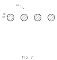
- FIG. 2 is a cross-sectional view along line II-II of FIG. 1 .
- FIG. 3 is a Scanning Electron Microscope (SEM) image of a drawn carbon nanotube film of one embodiment.
- FIG. 4 is an SEM image of an untwisted carbon nanotube wire of one embodiment.
- FIG. 5 is an SEM image of a twisted carbon nanotube wire of one embodiment.
- FIG. 6 is an SEM image of a carbon nanotube composite structure with cross-stacked drawn carbon nanotube films of one embodiment.
- FIG. 7 is an SEM image of a patterned surface fabricated by a method of one embodiment.
- FIG. 8 is a top view SEM image of a nano-pillar array fabricated by a method of one embodiment.
- FIG. 9 is a side view SEM image of a nano-pillar array fabricated by a method of one embodiment.
- FIG. 10 is a flowchart of another embodiment of a method for making a nano-pillar array on a surface of a substrate.
- FIG. 11 is a side view SEM image of a nano-pillar array fabricated by a method of one embodiment.
- FIG. 12 is an enlarged side view SEM image of a nano-pillar array of FIG. 11 .
- substantially is defined to be essentially conforming to the particular dimension, shape or other word that substantially modifies, such that the component need not be exact.
- substantially cylindrical means that the object resembles a cylinder, but can have one or more deviations from a true cylinder.
- comprising means “including, but not necessarily limited to”; it specifically indicates open-ended inclusion or membership in a so-described combination, group, series and the like. It should be noted that references to “an” or “one” embodiment in this disclosure are not necessarily to the same embodiment, and such references mean at least one.
- a method for making a nano-pillar array 105 on a surface of a substrate 100 of one embodiment includes the following steps: step (S 10 ), providing the substrate 100 ;
- step (S 11 ) providing a carbon nanotube composite structure 110 , wherein the carbon nanotube composite structure 110 includes a plurality of crossed carbon nanotubes and defines a plurality of openings 116 ;
- step (S 12 ) placing the carbon nanotube composite structure 110 on a surface 101 of the substrate 100 , wherein parts of the surface 101 are exposed from the plurality of openings 116 ;
- step (S 13 ) forming a patterned surface 103 on the substrate 100 by dry etching the surface 101 using the carbon nanotube composite structure 110 as a first mask, wherein the patterned surface 103 includes a plurality of strip-shaped bulges crossed with each other;
- step (S 15 ) applying a photoresist layer 120 on the patterned surface 103 ;
- step (S 16 ) removing the photoresist layer 120 and obtaining some residual photoresist 122 at intersections of the plurality of strip-shaped bulges;
- step (S 17 ) dry etching the substrate 100 using the residual photoresist 122 as a second mask.
- the material of the substrate 100 is not limited and can be metal, insulating material or semiconductor.
- the metal can be gold, aluminum, nickel, chromium, or copper.
- the insulating material can be silicon dioxide or silicon nitride.
- the semiconductor can be silicon, gallium nitride, or gallium arsenide.
- the material of the substrate 100 is a gallium nitride layer with a thickness of 300 micrometers.
- the carbon nanotube composite structure 110 includes a carbon nanotube structure 112 and a protective layer 114 coated on the carbon nanotube structure 112 as shown in FIG. 2 .
- the carbon nanotube structure 112 is a free-standing structure.
- the term “free-standing structure” includes that the carbon nanotube structure 112 can sustain the weight of itself when it is hoisted by a portion thereof without any significant damage to its structural integrity. Thus, the carbon nanotube structure 112 can be suspended by two spaced supports.
- the plurality of carbon nanotubes can be single-walled carbon nanotubes, double-walled carbon nanotubes, or multi-walled carbon nanotubes.
- the length and diameter of the plurality of carbon nanotubes can be selected according to need.
- the diameter of the single-walled carbon nanotubes can be in a range from about 0.5 nanometers to about 10 nanometers.
- the diameter of the double-walled carbon nanotubes can be in a range from about 1.0 nanometer to about 15 nanometers.
- the diameter of the multi-walled carbon nanotubes can be in a range from about 1.5 nanometers to about 50 nanometers.
- the length of the carbon nanotubes can be in a range from about 200 micrometers to about 900 micrometers.
- the plurality of carbon nanotubes are orderly arranged to form an ordered carbon nanotube structure.
- the plurality of carbon nanotubes extend along a direction substantially parallel to the surface of the carbon nanotube structure 112 .
- ordered carbon nanotube structure includes, but is not limited to, a structure wherein the plurality of carbon nanotubes are arranged in a consistently systematic manner, e.g., the plurality of carbon nanotubes are arranged approximately along the same direction.
- the carbon nanotube structure 112 defines a plurality of apertures.
- the aperture extends throughout the carbon nanotube structure 112 along the thickness direction thereof
- the aperture can be a hole defined by several adjacent carbon nanotubes, or a gap defined by two substantially parallel carbon nanotubes and extending along axial direction of the carbon nanotubes.
- the hole shaped aperture and the gap shaped aperture can exist in the carbon nanotube structure 112 at the same time.
- the size of the aperture is the diameter of the hole or width of the gap.
- the sizes of the apertures can be different.
- the average size of the apertures can be in a range from about 10 nanometers to about 500 micrometers.
- the sizes of the apertures can be about 50 nanometers, 100 nanometers, 500 nanometers, 1 micrometer, 10 micrometers, 80 micrometers, or 120 micrometers.
- the carbon nanotube structure 112 can include at least one carbon nanotube film, at least one carbon nanotube wire, or combination thereof.
- the carbon nanotube structure 112 can include a single carbon nanotube film or two or more carbon nanotube films stacked together.
- the thickness of the carbon nanotube structure 112 can be controlled by the number of the stacked carbon nanotube films.
- the number of the stacked carbon nanotube films can be in a range from about 2 to about 100.
- the number of the stacked carbon nanotube films can be 10, 30, or 50.
- the carbon nanotube structure 112 is formed by folding a single carbon nanotube wire.
- the carbon nanotube structure 112 can include a layer of parallel and spaced carbon nanotube wires.
- the carbon nanotube structure 112 can include a plurality of carbon nanotube wires crossed or weaved together to form a carbon nanotube net.
- the distance between two adjacent parallel and spaced carbon nanotube wires can be in a range from about 0.1 micrometers to about 200 micrometers. In one embodiment, the distance between two adjacent parallel and spaced carbon nanotube wires is in a range from about 10 micrometers to about 100 micrometers.
- the gap between two adjacent substantially parallel carbon nanotube wires is defined as the apertures.
- the size of the apertures can be controlled by controlling the distance between two adjacent parallel and spaced carbon nanotube wires.
- the length of the gap between two adjacent parallel carbon nanotube wires can be equal to the length of the carbon nanotube wire. It is understood that any carbon nanotube structure described can be used with all embodiments.
- the carbon nanotube structure 112 includes at least one drawn carbon nanotube film.
- the drawn carbon nanotube film can be drawn from a carbon nanotube array that is able to have a film drawn therefrom.
- the drawn carbon nanotube film includes a plurality of successive and oriented carbon nanotubes joined end-to-end by van der Waals attractive force therebetween.
- the drawn carbon nanotube film is a free-standing film. Referring to FIG. 3 , each drawn carbon nanotube film includes a plurality of successively oriented carbon nanotube segments joined end-to-end by van der Waals attractive force therebetween.
- Each carbon nanotube segment includes a plurality of carbon nanotubes parallel to each other, and combined by van der Waals attractive force therebetween. As can be seen in FIG.
- the carbon nanotubes in the drawn carbon nanotube film are oriented along a preferred orientation.
- the drawn carbon nanotube film can be treated with an organic solvent to increase the mechanical strength and toughness and reduce the coefficient of friction of the drawn carbon nanotube film.
- a thickness of the drawn carbon nanotube film can range from about 0.5 nanometers to about 100 micrometers.
- the drawn carbon nanotube film defines a plurality of apertures between adjacent carbon nanotubes.
- the carbon nanotube structure 112 can include at least two stacked drawn carbon nanotube films.
- the carbon nanotube structure 112 can include two or more coplanar carbon nanotube films, and can include layers of coplanar carbon nanotube films.
- an angle can exist between the orientation of carbon nanotubes in adjacent films, whether stacked or adjacent. Adjacent carbon nanotube films can be combined by only the van der Waals attractive force therebetween.
- An angle between the aligned directions of the carbon nanotubes in two adjacent carbon nanotube films can range from about 0 degrees to about 90 degrees.
- the carbon nanotube structure 112 When the angle between the aligned directions of the carbon nanotubes in adjacent stacked drawn carbon nanotube films is larger than 0 degrees, a plurality of micropores is defined by the carbon nanotube structure 112 .
- the carbon nanotube structure 112 has the aligned directions of the carbon nanotubes between adjacent stacked drawn carbon nanotube films at 90 degrees. Stacking the carbon nanotube films will also add to the structural integrity of the carbon nanotube structure 112 .
- the carbon nanotube wire can be untwisted or twisted. Treating the drawn carbon nanotube film with a volatile organic solvent can form the untwisted carbon nanotube wire. Specifically, the organic solvent is applied to soak the entire surface of the drawn carbon nanotube film. During the soaking, adjacent parallel carbon nanotubes in the drawn carbon nanotube film will bundle together, due to the surface tension of the organic solvent as it volatilizes, and thus, the drawn carbon nanotube film will be shrunk into an untwisted carbon nanotube wire.
- the untwisted carbon nanotube wire includes a plurality of carbon nanotubes substantially oriented along the same direction (i.e., a direction along the length of the untwisted carbon nanotube wire).
- the carbon nanotubes are substantially parallel to the axis of the untwisted carbon nanotube wire. More specifically, the untwisted carbon nanotube wire includes a plurality of successive carbon nanotube segments joined end to end by van der Waals attractive force therebetween. Each carbon nanotube segment includes a plurality of carbon nanotubes substantially parallel to each other, and combined by van der Waals attractive force therebetween.
- the carbon nanotube segments can vary in width, thickness, uniformity, and shape.
- the length of the untwisted carbon nanotube wire can be arbitrarily set as desired. A diameter of the untwisted carbon nanotube wire ranges from about 0.5 nanometers to about 100 micrometers.
- the twisted carbon nanotube wire can be formed by twisting a drawn carbon nanotube film using a mechanical force to turn the two ends of the drawn carbon nanotube film in opposite directions.
- the twisted carbon nanotube wire includes a plurality of carbon nanotubes helically oriented around an axial direction of the twisted carbon nanotube wire. More specifically, the twisted carbon nanotube wire includes a plurality of successive carbon nanotube segments joined end to end by van der Waals attractive force therebetween. Each carbon nanotube segment includes a plurality of carbon nanotubes parallel to each other, and combined by van der Waals attractive force therebetween.
- the length of the carbon nanotube wire can be set as desired.
- a diameter of the twisted carbon nanotube wire can be from about 0.5 nanometers to about 100 micrometers. Further, the twisted carbon nanotube wire can be treated with a volatile organic solvent after being twisted to bundle the adjacent paralleled carbon nanotubes together. The specific surface area of the twisted carbon nanotube wire will decrease, while the density and strength of the twisted carbon nanotube wire will increase.
- carbon nanotube composite structure 110 can be made by applying a protective layer 114 on a surface of the carbon nanotube structure 112 .
- the carbon nanotube structure 112 can be suspended in a depositing chamber during depositing the protective layer 114 so that two opposite surfaces of the carbon nanotube structure 112 are coated with the protective layer 114 .
- each of the plurality of carbon nanotubes is fully enclosed by the protective layer 114 .
- the carbon nanotube structure 112 is located on a frame so that the middle portion of the carbon nanotube structure 112 is suspended through the through hole of the frame.
- the frame can be any shape, such as a quadrilateral.
- the carbon nanotube structure 112 can also be suspended by a metal mesh or metal ring.
- the method of depositing the protective layer 114 can be physical vapor deposition (PVD), chemical vapor deposition (CVD), atomic layer deposition (ALD), magnetron sputtering, or spraying.
- PVD physical vapor deposition
- CVD chemical vapor deposition
- ALD atomic layer deposition
- magnetron sputtering or spraying.
- the plurality of openings 116 are formed because of the plurality of apertures of the carbon nanotube structure 112 .
- the plurality of openings 116 and the plurality of apertures have the same shape and different size.
- the size of the plurality of openings 116 is smaller than that of the plurality of apertures because the protective layer 114 is deposited in the plurality of apertures.
- the thickness of the protective layer 114 is in a range from about 3 nanometers to about 50 nanometers. In one embodiment, the thickness of the protective layer 114 is in a range from about 3 nanometers to about 20 nanometers. If the thickness of the protective layer 114 is less than 3 nanometers, the protective layer 114 cannot prevent the carbon nanotubes from being destroyed in following etching process. If the thickness of the protective layer 114 is greater than 50 nanometers, the plurality of apertures may be fully filled by the protective layer 114 and the plurality of openings 116 cannot be obtained.
- the material of the protective layer 114 can be metal, metal oxide, metal nitride, metal carbide, metal sulfide, silicon oxide, silicon nitride, or silicon carbide.
- the metal can be gold, nickel, titanium, iron, aluminum, titanium, chromium, or alloy thereof
- the metal oxide can be alumina, magnesium oxide, zinc oxide, or hafnium oxide.
- the material of the protective layer 114 is not limited above and can be any material as long as the material can be deposited on the carbon nanotube structure 112 , would not react with the carbon nanotubes and would not be etched easily in following drying etching process.
- the protective layer 114 is combined with the carbon nanotube structure 112 by van der Waals attractive force therebetween only.
- an alumina layer of 5 nanometers thickness is deposited on two stacked drawn carbon nanotube films by electron beam evaporation.
- the aligned direction of the carbon nanotubes between adjacent stacked drawn carbon nanotube films is 90 degrees.
- the carbon nanotube composite structure 110 can be in direct contact with the surface 101 of the substrate 100 or suspended above the surface 101 of the substrate 100 by a support. In one embodiment, the carbon nanotube composite structure 110 is transferred on the surface 101 of the substrate 100 through the frame.
- the placing the carbon nanotube composite structure 110 on the surface 101 comprises solvent treating the substrate 100 with the carbon nanotube composite structure 110 thereon. Because there is air between the carbon nanotube composite structure 110 and the surface 101 of the substrate 100 , the solvent treating can exhaust the air and allow the carbon nanotube composite structure 110 to be closely and firmly adhered on the surface 101 of the substrate 100 .
- the solvent treating can be applying a solvent to entire surface of the carbon nanotube composite structure 110 or immersing the entire substrate 100 with the carbon nanotube composite structure 110 in a solvent.
- the solvent can be water or volatile organic solvent such as ethanol, methanol, acetone, dichloroethane, chloroform, or mixtures thereof In one embodiment, the organic solvent is ethanol.
- the dry etching can be plasma etching or reactive ion etching (RIE).
- the dry etching is performed by applying plasma energy on the entire or part surface of the surface 101 via a plasma device.
- the plasma gas can be an inert gas and/or etching gases, such as argon (Ar), helium (He), chlorine (Cl 2 ), hydrogen (H 2 ), oxygen (O 2 ), fluorocarbon (CF 4 ), ammonia (NH 3 ), or air.
- the plasma gas is a mixture of chlorine and argon.
- the power of the plasma device can be in a range from about 20 watts to about 70 watts.
- the plasma flow of chlorine can be in a range from about 5 sccm to about 20 sccm, such as 10 sccm.
- the plasma flow of argon can be in a range from about 15 sccm to about 40 sccm, such as 25 sccm.
- the work pressure of the plasma can be in a range from about 3 Pa to 10 Pa, such as 6 Pa.
- the time for plasma etching can be in a range from about 10 seconds to about 20 seconds, such as 15 seconds.
- the plasma gas would react with the exposed portion of the substrate 100 and would not react with the protective layer 114 , or reaction between the plasma gas and the protective layer 114 is much slower than reaction between the plasma gas and the substrate 100 .
- the selection relationship of the plasma gas, material of the substrate 100 and material of the protective layer 114 is shown in Table 1 below.
- Substrate protective layer Plasma gas 1 Al SiO 2 Cl 2 or BCl 3 2 SiO 2 Al, Cr, Fe, Ti, Ni, or Au CF 4 3 SiN x Al, Cr, Fe, Ti, Ni, or Au CF 4 4 GaN Al 2 O 3 Cl 2 or Ar 2 5 Au, Cr or Ni SiO 2 or SiN x O 2 or Ar 2 6 Cu SiO 2 or SiN x O 2 or BCl 3
- the etching gas reacts with the substrate 100 , but does not react with the protective layer 114 or react with the protective layer 114 at a speed much less than that of the reaction between the etching gas and the substrate 100 .
- the exposed portion of the substrate 100 would be etched gradually and the portion of the substrate 100 that are shielded by the carbon nanotube composite structure 110 would not be etched.
- the patterned surface 103 and the carbon nanotube composite structure 110 substantially have the same pattern as shown in FIG. 6-7 .
- the carbon nanotube structure 112 includes a plurality of crossed drawn carbon nanotube films
- the patterned surface 103 includes a plurality of strip-shaped bulges crossed with each other.
- the width of the strip-shaped bulges can be in a range from about 20 nanometers to about 150 nanometers. In one embodiment, the width of the strip-shaped bulges can be in a range from about 20 nanometers to about 100 nanometers. In one embodiment, the width of the strip-shaped bulges can be in a range from about 50 nanometers to about 100 nanometers. The distance between adjacent two of the strip-shaped bulges can be in a range from about 10 nanometers to about 300 nanometers. In one embodiment, the distance between adjacent two of the strip-shaped bulges can be in a range from about 10 nanometers to about 100 nanometers.
- the distance between adjacent two of the strip-shaped bulges can be in a range from about 100 nanometers to about 200 nanometers.
- the height of the strip-shaped bulge is determined by the etching time and can be in a range from about 10 nanometers to about 100 nanometers. In one embodiment, the height of the strip-shaped bulge can be in a range from about 50 nanometers to about 60 nanometers.
- the patterned surface 103 includes a plurality of strip-shaped bulges crossed with each other.
- step (S 14 ) the method of removing the carbon nanotube composite structure 110 can be ultrasonic method, or adhesive tape peeling, oxidation.
- the substrate 100 with the carbon nanotube composite structure 110 thereon is placed in an N-methyl pyrrolidone solution and ultrasonic treating for several minutes.
- the method for applying the photoresist layer 120 can be spin coating, immersion coating or vapor deposition.
- the method for applying the photoresist layer 120 is not limited as long as the photoresist layer 120 can be formed on the patterned surface 103 .
- the thickness of the photoresist layer 120 can be in a range from about 1 micrometer to about 3 micrometers. In one embodiment, the photoresist layer 120 with a thickness of 1.5 micrometers is applied on the patterned surface 103 by spin coating.
- the method for removing the photoresist layer 120 can be exposure and development.
- the photoresist layer 120 is first exposed to the ultraviolet (UV) light for a time in a range from about 10 seconds to about 30 seconds and then developed in a sodium hydroxide (NaOH) solution of 0.05 mol/L ⁇ 0.3 mol/L concentration.
- the sodium hydroxide solution can remove most of the photoresist layer 120 on the patterned surface 103 .
- Some of the photoresist layer 120 that are at intersections of the plurality of strip-shaped bulges remains as the residual photoresist 122 .
- the substrate 100 after photoresist layer 120 being exposed to the ultraviolet light and developed in the sodium hydroxide solution, is further soaked in an acetone for 12 hours.
- the residual photoresist 122 is critical for making the nano-pillar array 105 on the substrate 100 .
- the photoresist layer 120 can be partially exposed to the ultraviolet light so as to make the nano-pillar array 105 on only part of the substrate 100 .
- the method for removing the photoresist layer 120 can be directly soaking the photoresist layer 120 in the acetone for a time in a range from about several seconds to about several hours without any exposure. Usually, it needs to soak the photoresist layer 120 in the acetone for a time more than 10 hours to completely remove the photoresist layer 120 . Therefore, it can only remove most of the photoresist layer 120 on the patterned surface 103 by directly soaking the photoresist layer 120 in the acetone for a time less than 10 hours. Some of the photoresist layer 120 that are at intersections of the plurality of strip-shaped bulges remains as the residual photoresist 122 .
- the photoresist layer 120 is directly soaked in the acetone for 20 seconds and the nano-pillar array 105 can be formed on the substrate 100 in following dry etching steps. In one embodiment, the photoresist layer 120 is directly soaked in the acetone for 5 hours, and the nano-pillar array 105 can also be formed on the substrate 100 in following dry etching steps. The density of the nano-pillar array 105 will be affected by the soaking time. The longer the photoresist layer 120 is soaked in the acetone, the less residual photoresist 122 will remain. Thus, the smaller the density of the nano-pillar array 105 will be.
- the photoresist layer 120 has larger contacting surfaces with the patterned surface 103 at intersections of the plurality of strip-shaped bulges, it is easy for some of the photoresist layer 120 that are at intersections of the plurality of strip-shaped bulges to remain as the residual photoresist 122 .
- step (S 17 ) the method for dry etching the substrate 100 using the residual photoresist 122 as mask is the same as the dry etching of step (S 13 ).
- the dry etching in step (S 17 ) has greater power and longer etching time that that of step (S 13 ).
- the plasma gas in step (S 17 ) is a mixture of chlorine and argon.
- the power of the plasma device can be in a range from about 20 watts to about 70 watts.
- the plasma flow of chlorine can be in a range from about 10 sccm to about 20 sccm, such as 10 sccm.
- the plasma flow of argon can be in a range from about 25 sccm to about 35 sccm, such as 30 sccm.
- the work pressure of the plasma can be in a range from about 5Pa to 10 Pa.
- the time for plasma etching can be in a range from about 3 minutes to about 10 minutes.
- a plurality of nano-pillars are formed at the intersections of the strip-shaped bulges to form the nano-pillar array 105 .
- Each of the plurality of nano-pillars corresponds to one intersection of the crossed carbon nanotubes of the carbon nanotube composite structure 110 .
- the method for making the nano-pillar array 105 is simple, low coast, and can make the nano-pillar array 105 in mass.
- the plurality of nano-pillars are distributed on the substrate.
- the plurality of nano-pillars are substantially parallel with, spaced from each other and perpendicular with the substrate.
- Each of the plurality of nano-pillars includes a half spherical plinth and a column located on the plinth.
- the height of the plinth is in a range from about 0.2 micrometer to about 0.5 micrometer.
- the height of the column is in a range from about 0.5 micrometers to about 2.5 micrometers.
- the diameter of the column is in a range from about 100 nanometers to about 300 nanometers.
- the ratio of the length to diameter of the column is greater than 4:1, such as greater than 8:1.
- the height of the plinth is 0.31 micrometers
- the height of the column is 1.17 micrometers
- the diameter of the column is 287 nanometers.
- a method for making a nano-pillar array 105 on a surface of a substrate 100 of one embodiment includes the following steps:
- step (S 20 ) applying a transition layer 102 on the surface 101 of the substrate 100 ;
- step (S 21 ) placing the carbon nanotube composite structure 110 on the transition layer 102 , wherein parts of the transition layer 102 are exposed from the plurality of openings 116 ;
- step (S 22 ) forming a patterned transition layer 104 on the substrate 100 by dry etching the transition layer 102 using the carbon nanotube composite structure 110 as a first mask;
- step (S 23 ) exposing the patterned transition layer 104 by removing the carbon nanotube composite structure 110 ;
- step (S 24 ) forming a patterned surface 103 on the substrate 100 by dry etching the surface 101 using the patterned transition layer 104 as a second mask, wherein the patterned surface 103 includes a plurality of strip-shaped bulges crossed with each other;
- step (S 25 ) exposing the patterned surface 103 by removing the patterned transition layer 104 ;
- step (S 27 ) removing the photoresist layer 120 and obtaining some residual photoresist 122 at intersections of the plurality of strip-shaped bulges;
- step (S 28 ) dry etching the substrate 100 using the residual photoresist 122 as a third mask.
- the method of FIG. 10 is similar as the method of FIG. 1 except that the pattern of the carbon nanotube composite structure 110 is transferred on the transition layer 102 to form the patterned transition layer 104 first, and then the pattern of the patterned transition layer 104 is transferred on surface 101 of the substrate 100 to form the patterned surface 103 .
- the pattern of the carbon nanotube composite structure 110 is transferred on the transition layer 102 to form the patterned transition layer 104 first, and then the pattern of the patterned transition layer 104 is transferred on surface 101 of the substrate 100 to form the patterned surface 103 .
- long time and high temperatures are required to dry etch the surface 101 of the substrate 100 in order to make the patterned surface 103 .
- the carbon nanotube composite structure 110 is used as the mask to directly dry etch the surface 101 of the substrate 100 , the carbon nanotube composite structure 110 would be damaged and attached on the substrate 100 closely and firmly. Thus, it would be hard to remove the carbon nanotube composite structure 110 .
- the material of the transition layer 102 is not limited and can be any material that can be deposited on the surface 101 and etched by the dry etching.
- the material of the transition layer 102 can be hafnium oxide, alumina, silica, aluminum, or gold.
- the shape, thickness and size of the transition layer 102 are not limited.
- the substrate 100 is a gallium arsenide layer with a thickness of 300 micrometers
- the transition layer 102 is a silicon dioxide layer with a thickness of 20 nanometers.
- the silicon dioxide layer cover entire surface 101 of the gallium arsenide layer.
- step (S 22 ) the method of dry etching the transition layer 102 is the same as the dry etching of step (S 13 ).
- the etching gas reacts with the exposed transition layer 102 , but does not react with the protective layer 114 or react with the protective layer 114 at a speed much less than that of the reaction between the etching gas and the transition layer 102 .
- the pattern of the patterned transition layer 104 is the same as that of the carbon nanotube composite structure 110 .
- the plasma gas for etching the transition layer 102 is CF 4 .
- the power of the plasma device can be in a range from about 30 watts to about 50 watts.
- the plasma flow of CF 4 can be in a range from about 30 sccm to about 50 sccm.
- the work pressure of the plasma can be in a range from about 1.5 Pa to 3 Pa.
- the time for plasma etching can be in a range from about 5 seconds to about 20 seconds.
- the patterned transition layer 104 includes a plurality of nano-bars crossed with each other to form a net structure.
- the patterned transition layer 104 defines a plurality of opening to expose parts of the surface 101 .
- the width of the nano-bar can be in a range from about 20 nanometers to about 150 nanometers, such as from about 20 nanometers to about 100 nanometers.
- the distance between adjacent two of the nano-bars can be in a range from about 10 nanometers to about 300 nanometers, such as from about 20 nanometers to about 100 nanometers.
- the height of the nano-bar is the same as the thickness of the transition layer 102 .
- step (S 24 ) the method of dry etching the surface 101 is the same as the dry etching of step (S 13 ).
- the etching gas reacts with the exposed surface 101 , but does not react with the patterned transition layer 104 or react with the patterned transition layer 104 at a speed much less than that of the reaction between the etching gas and the surface 101 .
- the pattern of the patterned surface 103 is the same as that of the carbon nanotube composite structure 110 and the patterned transition layer 104 .
- the method of removing the patterned transition layer 104 can be wet etching.
- the patterned transition layer 104 is removed by etching in a hydrofluoric (HF) acid solution.
- the plurality of nano-pillars are substantially parallel with, spaced from each other and perpendicular with the substrate.
- Each of the plurality of nano-pillars comprises a half spherical plinth and a column located on the plinth. The ratio of the length to diameter of the column is greater than 6:1.
Landscapes
- Physics & Mathematics (AREA)
- General Physics & Mathematics (AREA)
- Engineering & Computer Science (AREA)
- Plasma & Fusion (AREA)
- Chemical & Material Sciences (AREA)
- Analytical Chemistry (AREA)
- Carbon And Carbon Compounds (AREA)
Applications Claiming Priority (3)
| Application Number | Priority Date | Filing Date | Title |
|---|---|---|---|
| CN201410660932.9A CN105668540B (zh) | 2014-11-19 | 2014-11-19 | 一种纳米线阵列的制备方法 |
| CN201410660932 | 2014-11-19 | ||
| CN201410660932.9 | 2014-11-19 |
Publications (2)
| Publication Number | Publication Date |
|---|---|
| US20160139511A1 US20160139511A1 (en) | 2016-05-19 |
| US9417531B2 true US9417531B2 (en) | 2016-08-16 |
Family
ID=55961566
Family Applications (1)
| Application Number | Title | Priority Date | Filing Date |
|---|---|---|---|
| US14/832,494 Active US9417531B2 (en) | 2014-11-19 | 2015-08-21 | Method for making nano-pillar array on substrate |
Country Status (3)
| Country | Link |
|---|---|
| US (1) | US9417531B2 (zh) |
| CN (1) | CN105668540B (zh) |
| TW (1) | TWI557067B (zh) |
Families Citing this family (17)
| Publication number | Priority date | Publication date | Assignee | Title |
|---|---|---|---|---|
| WO2016093039A1 (ja) * | 2014-12-09 | 2016-06-16 | コニカミノルタ株式会社 | 検出チップおよび検出方法 |
| CN106276778B (zh) * | 2015-05-21 | 2018-08-14 | 清华大学 | 一种金属纳米线膜的制备方法以及导电元件 |
| CN107469478B (zh) * | 2016-06-07 | 2023-06-06 | 苏州苏瑞膜纳米科技有限公司 | 流体处理装置及其制备方法 |
| CN108072640B (zh) * | 2016-11-14 | 2020-01-07 | 清华大学 | 一种单分子检测装置以及单分子检测方法 |
| CN107561051A (zh) * | 2016-07-01 | 2018-01-09 | 清华大学 | 一种用于单分子检测的分子载体 |
| CN107561053B (zh) * | 2016-07-01 | 2020-04-28 | 清华大学 | 一种单分子检测方法 |
| CN107561052B (zh) | 2016-07-01 | 2020-04-28 | 清华大学 | 一种用于单分子检测的分子载体的制备方法 |
| CN108132582B (zh) * | 2016-12-01 | 2020-06-09 | 清华大学 | 光刻掩模板 |
| CN108132581B (zh) * | 2016-12-01 | 2020-07-10 | 清华大学 | 光刻掩模板 |
| CN108132579B (zh) * | 2016-12-01 | 2020-09-25 | 清华大学 | 光刻掩模板 |
| CN108987647B (zh) * | 2017-06-05 | 2020-07-10 | 清华大学 | 锂硫电池隔膜的制备方法 |
| CN109470679B (zh) * | 2017-09-08 | 2021-04-23 | 清华大学 | 用于分子检测的分子载体 |
| CN109470676A (zh) * | 2017-09-08 | 2019-03-15 | 清华大学 | 用于分子检测的分子载体 |
| CN111482149A (zh) | 2019-01-25 | 2020-08-04 | 清华大学 | 光催化结构及其制备方法 |
| CN111489897B (zh) | 2019-01-25 | 2022-06-21 | 清华大学 | 光催化结构及其制备方法 |
| CN113823992B (zh) * | 2021-09-14 | 2022-11-11 | 苏州长瑞光电有限公司 | 半导体器件制造方法及半导体器件 |
| CN114538413A (zh) * | 2021-11-19 | 2022-05-27 | 昆明理工大学 | 一种大面积纳米线阵列膜及其制备方法 |
Citations (1)
| Publication number | Priority date | Publication date | Assignee | Title |
|---|---|---|---|---|
| US20150279657A1 (en) * | 2014-03-27 | 2015-10-01 | Tsinghua University | Method for making epitaxial structure |
Family Cites Families (16)
| Publication number | Priority date | Publication date | Assignee | Title |
|---|---|---|---|---|
| CN100560811C (zh) * | 2004-08-28 | 2009-11-18 | 清华大学 | 硅纳米线结构及其生长方法 |
| CN1309027C (zh) * | 2004-09-02 | 2007-04-04 | 上海交通大学 | 基于纳米材料排布的纳米刻蚀方法 |
| SG149036A1 (en) * | 2005-03-17 | 2009-01-29 | Agency Science Tech & Res | A method of fabricating periodic nano-structure arrays with different feature sizes |
| KR101343362B1 (ko) * | 2007-12-20 | 2013-12-20 | 삼성전자주식회사 | 메모리 유닛의 제조 방법, 이에 따라 제조된 메모리 유닛,메모리 장치의 제조 방법 및 이에 따라 제조된 메모리 장치 |
| KR101094376B1 (ko) * | 2009-07-31 | 2011-12-15 | 주식회사 하이닉스반도체 | 반도체장치의 매립워드라인 형성 방법 |
| US8557613B2 (en) * | 2010-06-14 | 2013-10-15 | California Institute Of Technology | Methods for designing, fabricating, and predicting shape formations in a material |
| US8961799B2 (en) * | 2010-10-21 | 2015-02-24 | Hewlett-Packard Development Company, L.P. | Nano-structured surface |
| US20120171755A1 (en) * | 2011-01-03 | 2012-07-05 | Technion Research And Development Foundation Ltd. | Fabrication of hollow nanoneedles |
| US9024310B2 (en) * | 2011-01-12 | 2015-05-05 | Tsinghua University | Epitaxial structure |
| CN103030106B (zh) * | 2011-10-06 | 2015-04-01 | 清华大学 | 三维纳米结构阵列 |
| CN103359719B (zh) * | 2012-04-05 | 2015-01-21 | 清华大学 | 石墨烯纳米窄带的制备方法 |
| CN103359717B (zh) * | 2012-04-05 | 2015-06-03 | 清华大学 | 石墨烯纳米窄带的制备方法 |
| CN103359723B (zh) * | 2012-04-05 | 2015-01-21 | 清华大学 | 石墨烯纳米窄带的制备方法 |
| WO2014176409A1 (en) * | 2013-04-24 | 2014-10-30 | Natcore Technology, Inc. | Solar cells with patterned antireflective surfaces |
| CN103681356A (zh) * | 2013-12-27 | 2014-03-26 | 上海集成电路研发中心有限公司 | 以碳纳米管为掩膜制备FinFET的方法 |
| CN103715098B (zh) * | 2013-12-27 | 2019-03-19 | 上海集成电路研发中心有限公司 | 以碳纳米管为掩膜制备鳍形结构的方法 |
-
2014
- 2014-11-19 CN CN201410660932.9A patent/CN105668540B/zh active Active
-
2015
- 2015-01-06 TW TW104100241A patent/TWI557067B/zh active
- 2015-08-21 US US14/832,494 patent/US9417531B2/en active Active
Patent Citations (1)
| Publication number | Priority date | Publication date | Assignee | Title |
|---|---|---|---|---|
| US20150279657A1 (en) * | 2014-03-27 | 2015-10-01 | Tsinghua University | Method for making epitaxial structure |
Also Published As
| Publication number | Publication date |
|---|---|
| TWI557067B (zh) | 2016-11-11 |
| CN105668540B (zh) | 2017-11-14 |
| TW201619044A (zh) | 2016-06-01 |
| CN105668540A (zh) | 2016-06-15 |
| US20160139511A1 (en) | 2016-05-19 |
Similar Documents
| Publication | Publication Date | Title |
|---|---|---|
| US9417531B2 (en) | Method for making nano-pillar array on substrate | |
| US9695506B2 (en) | Method for making microstructure on substrate | |
| US10124561B2 (en) | Metal nanowires structure | |
| US11947261B2 (en) | Method for making photolithography mask plate | |
| US11947255B2 (en) | Method for making photolithography mask plate | |
| US10145798B2 (en) | Carrier for single molecule detection | |
| US10877187B2 (en) | Hydrophobic mirror and vehicle using the same | |
| US10372031B2 (en) | Method for making microstructures | |
| US10533948B2 (en) | Carrier for use in single molecule detection | |
| US20150351285A1 (en) | Heat dissipation structure and synthesizing method thereof | |
| US20150144979A1 (en) | Nanostructure layer and light emitting diode with the same | |
| US10859501B2 (en) | Carrier for use in single molecule detection | |
| US10145797B2 (en) | Method for detecting single molecule | |
| US9611536B2 (en) | Method for making nanostructures | |
| US11747730B2 (en) | Method for making photolithography mask plate | |
| US10100436B2 (en) | Method for making gallium nitride epitaxial layer by silicon substrate | |
| US10132756B2 (en) | Method for making carrier for single molecule detection | |
| US10151704B2 (en) | Device for single molecule detection | |
| US11376577B2 (en) | Photocatalytic structure and method for making the same | |
| Wang et al. | Process and characteristics of the large area well-aligned CNTs with open ends by electron cyclotron resonance chemical vapor deposition | |
| Chang et al. | Field emission properties of carbon nanotube arrays on the thickness-controlled flexible substrate by the pattern transfer process |
Legal Events
| Date | Code | Title | Description |
|---|---|---|---|
| AS | Assignment |
Owner name: TSINGHUA UNIVERSITY, CHINA Free format text: ASSIGNMENT OF ASSIGNORS INTEREST;ASSIGNORS:LI, QUN-QING;JIN, YUAN-HAO;FAN, SHOU-SHAN;REEL/FRAME:036393/0041 Effective date: 20150817 Owner name: HON HAI PRECISION INDUSTRY CO., LTD., TAIWAN Free format text: ASSIGNMENT OF ASSIGNORS INTEREST;ASSIGNORS:LI, QUN-QING;JIN, YUAN-HAO;FAN, SHOU-SHAN;REEL/FRAME:036393/0041 Effective date: 20150817 |
|
| STCF | Information on status: patent grant |
Free format text: PATENTED CASE |
|
| MAFP | Maintenance fee payment |
Free format text: PAYMENT OF MAINTENANCE FEE, 4TH YEAR, LARGE ENTITY (ORIGINAL EVENT CODE: M1551); ENTITY STATUS OF PATENT OWNER: LARGE ENTITY Year of fee payment: 4 |
|
| MAFP | Maintenance fee payment |
Free format text: PAYMENT OF MAINTENANCE FEE, 8TH YEAR, LARGE ENTITY (ORIGINAL EVENT CODE: M1552); ENTITY STATUS OF PATENT OWNER: LARGE ENTITY Year of fee payment: 8 |