US9384696B2 - Display device, method of calculating compensation data thereof, and driving method thereof - Google Patents
Display device, method of calculating compensation data thereof, and driving method thereof Download PDFInfo
- Publication number
- US9384696B2 US9384696B2 US14/553,106 US201414553106A US9384696B2 US 9384696 B2 US9384696 B2 US 9384696B2 US 201414553106 A US201414553106 A US 201414553106A US 9384696 B2 US9384696 B2 US 9384696B2
- Authority
- US
- United States
- Prior art keywords
- temperature
- voltage
- temp
- voltage value
- compensation
- Prior art date
- Legal status (The legal status is an assumption and is not a legal conclusion. Google has not performed a legal analysis and makes no representation as to the accuracy of the status listed.)
- Active, expires
Links
- 238000000034 method Methods 0.000 title claims description 43
- 230000015556 catabolic process Effects 0.000 claims description 71
- 238000006731 degradation reaction Methods 0.000 claims description 71
- 230000006870 function Effects 0.000 claims description 33
- 230000010354 integration Effects 0.000 description 16
- 238000005259 measurement Methods 0.000 description 13
- 239000000463 material Substances 0.000 description 6
- 230000002277 temperature effect Effects 0.000 description 4
- 238000001514 detection method Methods 0.000 description 3
- 230000000694 effects Effects 0.000 description 3
- 230000004044 response Effects 0.000 description 2
- 230000002411 adverse Effects 0.000 description 1
- 238000004364 calculation method Methods 0.000 description 1
- 230000007423 decrease Effects 0.000 description 1
- 238000010586 diagram Methods 0.000 description 1
- 238000012886 linear function Methods 0.000 description 1
- 239000004973 liquid crystal related substance Substances 0.000 description 1
- 239000011159 matrix material Substances 0.000 description 1
- 230000003068 static effect Effects 0.000 description 1
Images

Classifications
-
- G—PHYSICS
- G09—EDUCATION; CRYPTOGRAPHY; DISPLAY; ADVERTISING; SEALS
- G09G—ARRANGEMENTS OR CIRCUITS FOR CONTROL OF INDICATING DEVICES USING STATIC MEANS TO PRESENT VARIABLE INFORMATION
- G09G3/00—Control arrangements or circuits, of interest only in connection with visual indicators other than cathode-ray tubes
- G09G3/20—Control arrangements or circuits, of interest only in connection with visual indicators other than cathode-ray tubes for presentation of an assembly of a number of characters, e.g. a page, by composing the assembly by combination of individual elements arranged in a matrix no fixed position being assigned to or needed to be assigned to the individual characters or partial characters
- G09G3/22—Control arrangements or circuits, of interest only in connection with visual indicators other than cathode-ray tubes for presentation of an assembly of a number of characters, e.g. a page, by composing the assembly by combination of individual elements arranged in a matrix no fixed position being assigned to or needed to be assigned to the individual characters or partial characters using controlled light sources
- G09G3/30—Control arrangements or circuits, of interest only in connection with visual indicators other than cathode-ray tubes for presentation of an assembly of a number of characters, e.g. a page, by composing the assembly by combination of individual elements arranged in a matrix no fixed position being assigned to or needed to be assigned to the individual characters or partial characters using controlled light sources using electroluminescent panels
- G09G3/32—Control arrangements or circuits, of interest only in connection with visual indicators other than cathode-ray tubes for presentation of an assembly of a number of characters, e.g. a page, by composing the assembly by combination of individual elements arranged in a matrix no fixed position being assigned to or needed to be assigned to the individual characters or partial characters using controlled light sources using electroluminescent panels semiconductive, e.g. using light-emitting diodes [LED]
- G09G3/3208—Control arrangements or circuits, of interest only in connection with visual indicators other than cathode-ray tubes for presentation of an assembly of a number of characters, e.g. a page, by composing the assembly by combination of individual elements arranged in a matrix no fixed position being assigned to or needed to be assigned to the individual characters or partial characters using controlled light sources using electroluminescent panels semiconductive, e.g. using light-emitting diodes [LED] organic, e.g. using organic light-emitting diodes [OLED]
- G09G3/3275—Details of drivers for data electrodes
- G09G3/3283—Details of drivers for data electrodes in which the data driver supplies a variable data current for setting the current through, or the voltage across, the light-emitting elements
-
- G—PHYSICS
- G09—EDUCATION; CRYPTOGRAPHY; DISPLAY; ADVERTISING; SEALS
- G09G—ARRANGEMENTS OR CIRCUITS FOR CONTROL OF INDICATING DEVICES USING STATIC MEANS TO PRESENT VARIABLE INFORMATION
- G09G3/00—Control arrangements or circuits, of interest only in connection with visual indicators other than cathode-ray tubes
- G09G3/20—Control arrangements or circuits, of interest only in connection with visual indicators other than cathode-ray tubes for presentation of an assembly of a number of characters, e.g. a page, by composing the assembly by combination of individual elements arranged in a matrix no fixed position being assigned to or needed to be assigned to the individual characters or partial characters
- G09G3/22—Control arrangements or circuits, of interest only in connection with visual indicators other than cathode-ray tubes for presentation of an assembly of a number of characters, e.g. a page, by composing the assembly by combination of individual elements arranged in a matrix no fixed position being assigned to or needed to be assigned to the individual characters or partial characters using controlled light sources
- G09G3/30—Control arrangements or circuits, of interest only in connection with visual indicators other than cathode-ray tubes for presentation of an assembly of a number of characters, e.g. a page, by composing the assembly by combination of individual elements arranged in a matrix no fixed position being assigned to or needed to be assigned to the individual characters or partial characters using controlled light sources using electroluminescent panels
- G09G3/32—Control arrangements or circuits, of interest only in connection with visual indicators other than cathode-ray tubes for presentation of an assembly of a number of characters, e.g. a page, by composing the assembly by combination of individual elements arranged in a matrix no fixed position being assigned to or needed to be assigned to the individual characters or partial characters using controlled light sources using electroluminescent panels semiconductive, e.g. using light-emitting diodes [LED]
- G09G3/3208—Control arrangements or circuits, of interest only in connection with visual indicators other than cathode-ray tubes for presentation of an assembly of a number of characters, e.g. a page, by composing the assembly by combination of individual elements arranged in a matrix no fixed position being assigned to or needed to be assigned to the individual characters or partial characters using controlled light sources using electroluminescent panels semiconductive, e.g. using light-emitting diodes [LED] organic, e.g. using organic light-emitting diodes [OLED]
- G09G3/3225—Control arrangements or circuits, of interest only in connection with visual indicators other than cathode-ray tubes for presentation of an assembly of a number of characters, e.g. a page, by composing the assembly by combination of individual elements arranged in a matrix no fixed position being assigned to or needed to be assigned to the individual characters or partial characters using controlled light sources using electroluminescent panels semiconductive, e.g. using light-emitting diodes [LED] organic, e.g. using organic light-emitting diodes [OLED] using an active matrix
- G09G3/3258—Control arrangements or circuits, of interest only in connection with visual indicators other than cathode-ray tubes for presentation of an assembly of a number of characters, e.g. a page, by composing the assembly by combination of individual elements arranged in a matrix no fixed position being assigned to or needed to be assigned to the individual characters or partial characters using controlled light sources using electroluminescent panels semiconductive, e.g. using light-emitting diodes [LED] organic, e.g. using organic light-emitting diodes [OLED] using an active matrix with pixel circuitry controlling the voltage across the light-emitting element
-
- G—PHYSICS
- G09—EDUCATION; CRYPTOGRAPHY; DISPLAY; ADVERTISING; SEALS
- G09G—ARRANGEMENTS OR CIRCUITS FOR CONTROL OF INDICATING DEVICES USING STATIC MEANS TO PRESENT VARIABLE INFORMATION
- G09G2300/00—Aspects of the constitution of display devices
- G09G2300/08—Active matrix structure, i.e. with use of active elements, inclusive of non-linear two terminal elements, in the pixels together with light emitting or modulating elements
- G09G2300/0809—Several active elements per pixel in active matrix panels
- G09G2300/0819—Several active elements per pixel in active matrix panels used for counteracting undesired variations, e.g. feedback or autozeroing
-
- G—PHYSICS
- G09—EDUCATION; CRYPTOGRAPHY; DISPLAY; ADVERTISING; SEALS
- G09G—ARRANGEMENTS OR CIRCUITS FOR CONTROL OF INDICATING DEVICES USING STATIC MEANS TO PRESENT VARIABLE INFORMATION
- G09G2320/00—Control of display operating conditions
- G09G2320/02—Improving the quality of display appearance
- G09G2320/0233—Improving the luminance or brightness uniformity across the screen
-
- G—PHYSICS
- G09—EDUCATION; CRYPTOGRAPHY; DISPLAY; ADVERTISING; SEALS
- G09G—ARRANGEMENTS OR CIRCUITS FOR CONTROL OF INDICATING DEVICES USING STATIC MEANS TO PRESENT VARIABLE INFORMATION
- G09G2320/00—Control of display operating conditions
- G09G2320/02—Improving the quality of display appearance
- G09G2320/0257—Reduction of after-image effects
-
- G—PHYSICS
- G09—EDUCATION; CRYPTOGRAPHY; DISPLAY; ADVERTISING; SEALS
- G09G—ARRANGEMENTS OR CIRCUITS FOR CONTROL OF INDICATING DEVICES USING STATIC MEANS TO PRESENT VARIABLE INFORMATION
- G09G2320/00—Control of display operating conditions
- G09G2320/02—Improving the quality of display appearance
- G09G2320/0285—Improving the quality of display appearance using tables for spatial correction of display data
-
- G—PHYSICS
- G09—EDUCATION; CRYPTOGRAPHY; DISPLAY; ADVERTISING; SEALS
- G09G—ARRANGEMENTS OR CIRCUITS FOR CONTROL OF INDICATING DEVICES USING STATIC MEANS TO PRESENT VARIABLE INFORMATION
- G09G2320/00—Control of display operating conditions
- G09G2320/02—Improving the quality of display appearance
- G09G2320/029—Improving the quality of display appearance by monitoring one or more pixels in the display panel, e.g. by monitoring a fixed reference pixel
- G09G2320/0295—Improving the quality of display appearance by monitoring one or more pixels in the display panel, e.g. by monitoring a fixed reference pixel by monitoring each display pixel
-
- G—PHYSICS
- G09—EDUCATION; CRYPTOGRAPHY; DISPLAY; ADVERTISING; SEALS
- G09G—ARRANGEMENTS OR CIRCUITS FOR CONTROL OF INDICATING DEVICES USING STATIC MEANS TO PRESENT VARIABLE INFORMATION
- G09G2320/00—Control of display operating conditions
- G09G2320/04—Maintaining the quality of display appearance
- G09G2320/041—Temperature compensation
-
- G—PHYSICS
- G09—EDUCATION; CRYPTOGRAPHY; DISPLAY; ADVERTISING; SEALS
- G09G—ARRANGEMENTS OR CIRCUITS FOR CONTROL OF INDICATING DEVICES USING STATIC MEANS TO PRESENT VARIABLE INFORMATION
- G09G2320/00—Control of display operating conditions
- G09G2320/04—Maintaining the quality of display appearance
- G09G2320/043—Preventing or counteracting the effects of ageing
- G09G2320/045—Compensation of drifts in the characteristics of light emitting or modulating elements
Definitions
- One or more embodiments described herein relate to a display device a method for calculating compensation data of a display device, and a method for driving a display device.
- a variety of displays have been developed. Examples include a liquid crystal display and an organic electroluminescent (EL) display.
- An organic EL display is thin and operates at low power levels.
- each of the light emitting devices of the display experiences stress.
- the amount of degradation of the light emitting devices may differ based on differences in the amount of stress accumulated for each pixel.
- the amount of stress is proportional to the product of luminance (e.g., amount of current flowing into the light emitting device) and time.
- the luminance and amount of stress accumulated for each pixel may also differ for different display patterns.
- the amount of degradation experienced by each pixel may be non-uniform. Also, after a predetermined time passes, an image sticking phenomenon may occur, even though the same data voltage is applied to each pixel. As a result, the quality or reliability of the display may be degraded.
- a display device includes a pixel, a sensing driver to measure a first voltage value applied to a light emitter in the pixel, a memory to store a second voltage value previously measured for the pixel, a first compensator to calculate a temperature of the light emitter at a time of measuring the first voltage value, and to compensate for the first voltage value based on the temperature, and a second compensator to compensate for input data for the pixel based on a voltage variation obtained from the temperature-compensated first voltage value and the second voltage value.
- the second voltage value may be a value temperature-compensated by the first compensator.
- the device may include operation logic to calculate the voltage variation from the first and second voltage values, to calculate an amount of luminance degradation from the voltage variation based on a first function, and to calculate a compensation current and compensation voltage data from the luminance degradation amount based on a second function, wherein the second compensator is to compensate for the input data based on the compensation voltage data.
- a method of calculating compensation data of a display device includes measuring a first voltage value applied to a light emitter in a pixel, calculating a temperature of the light emitter at a time of measuring the first voltage value, compensating for the first voltage value based on the temperature, calculating a voltage variation based on the temperature-compensated first voltage value and a second voltage value previously measured and stored in a memory for each of the pixels, and compensating for input data for the pixel based on the voltage variation.
- the second voltage value may be a value compensated based on the light emitter at a time of measuring the second voltage value.
- Compensating for the input data may include calculating an amount of luminance degradation from the voltage variation based on the first function, calculating a compensation current from the luminance degradation amount based on the second function, adjusting compensation voltage data based on the compensation current, and compensating for the input data based on the compensation voltage data.
- a driving method of a display device includes measuring a first voltage value applied to a light emitter in a pixel, calculating a temperature of the light emitter at a time of measuring the first voltage value, compensating for the first voltage value based on the temperature, calculating a voltage variation based on the temperature-compensated first voltage value and a second voltage value previously measured and stored in a memory, and compensating for input data for the pixel based on the voltage variation.
- the second voltage value may be a value compensated based on the temperature of the light emitter at a time of measuring the second voltage value.
- Compensating for the input data may includes calculating an amount of luminance degradation from the voltage variation based on the first function, calculating a compensation current from the luminance degradation amount based on, adjusting compensation voltage data to the compensation current, and compensating for the input data based on the compensation voltage data.
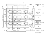
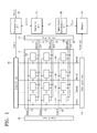
- FIG. 1 illustrates an embodiment of a display device
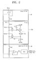
- FIG. 2 illustrates embodiments of a pixel, a data driver, and a sensing driver
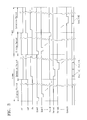
- FIG. 3 illustrates an embodiment of a method for driving a display device
- FIG. 4 illustrates an embodiment of a pixel circuit
- FIG. 5 illustrates an example of operation points of a pixel circuit
- FIG. 6 illustrates an example of a relationship between time and luminance degradation in a display device
- FIG. 7 illustrates an example of a relationship between time and an anode voltage in a display device
- FIG. 8 illustrates a change in a voltage-current characteristic for one embodiment of a light emitting device
- FIG. 9 illustrates a change in voltage-luminance characteristic for one embodiment of a light emitting device
- FIG. 10 illustrates a change in anode voltage based on pixel circuit configuration and temperature variation in one embodiment of a display device
- FIG. 11 illustrates a change in voltage-current characteristic for one embodiment of a light emitting device
- FIG. 12 illustrates a change in anode voltage for one embodiment of a light emitting device
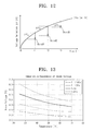
- FIG. 13 illustrates an example of temperature dependence of an anode voltage for a light emitting device
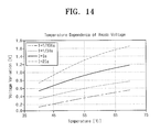
- FIG. 14 illustrates an example of temperature dependence of an anode voltage variation for a light emitting device
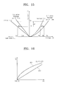
- FIG. 15 illustrates a change in voltage-current-luminance characteristic for one embodiment of a light emitting device according to time variation
- FIG. 16 illustrates an example of a relationship between voltage variation and luminance variation for one embodiment of a display device
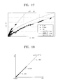
- FIG. 17 illustrates actually measured data and fitting data of voltage variation and luminance variation of RGB pixels for one embodiment of a display device
- FIG. 18 illustrates gradation dependence of a relationship between a voltage variation and a luminance variation for one embodiment of a display device
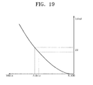
- FIG. 19 illustrates a relationship between compensation current and compensation voltage for one embodiment of a display device
- FIG. 20 illustrates an embodiment of a method for performing compensation in a display device
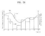
- FIG. 21 illustrates a relationship between a data integration value and pixel temperature for one embodiment of a display device
- the display unit 10 includes a plurality of pixels 100 .
- the pixels 100 are arrayed in a matrix shape of N rows and M columns, where N and M are natural numbers.
- the scan drivers 20 and 30 control each of the plurality of pixels 100 .
- the data driver 40 outputs data for determining pixel gradation.
- the sensing driver 50 measures voltages (e.g., anode voltages) applied to a light emitting device disposed in each of the pixels 100 and outputs the measured data Dva[1:M].
- the measured data Dva[1:M] measured by the sensing driver 50 is stored in the memory 60 .
- the temperature compensation unit 90 calculates a temperature of the light emitting device at the time of past and current measurements of the anode voltage, by using the data measured in the past and current time and stored in the memory 60 . In addition, the temperature compensation unit 90 temperature-compensates for the past and current anode voltages Voled on the basis of the calculated temperature. Past and current reference anode voltages V RT temperature-compensated by the temperature compensation unit 90 are provided to the operation unit 70 .
- the operation unit 70 outputs compensation voltage data ⁇ data on the basis of voltage variations, which, for example, may be obtained from past and current reference anode voltages V RT .
- the operation unit may be operation logic which, for example, may include hardware circuits, software, or a combination of both.
- the compensation unit 80 compensates for input data Idata received externally on the basis of the compensation voltage data ⁇ data, and outputs compensated image data Cdata.
- anode voltages Voled before temperature-compensation are stored in the memory 60 .
- the temperature-compensated reference anode voltage V RT may also be stored in the memory 60 , or in another memory or storage device.
- the scan driver 20 applies gate control signals Scan 1 to ScanN to control signal lines 21 to 23 corresponding to each row of pixels 100 .
- the scan driver 30 applies emission control signals En 1 to EnN to emission control lines 31 to 33 , and provides sensing control signals Sense 1 to SenseN to sensing control lines 51 to 53 .
- the pixels 100 receiving the gate control signals Scan 1 to ScanN and emission control signals En 1 to EnN receive data voltages Data 1 to DataM output from the data driver 40 through data lines 41 to 44 .
- An anode voltage of a light emitting device of each of the pixels 100 which receive the sensing control signals Sense 1 to SenseN, is measured by the sensing driver 50 through the data lines 41 to 44 .
- the measured anode voltage are output as the measured data Dva[1:M], and are stored in the memory 60 .
- the light emitting device of each of the pixels 100 includes a light emitting diode.
- the light emitting diode may be an organic light emitting diode (OLED).
- OLED organic light emitting diode
- a different type of light-emitting device may be used.
- FIG. 2 illustrates embodiments of the pixel 100 , the data driver 40 , and the sensing driver 50 in FIG. 1 .
- the pixel 100 includes the light emitting device, a driving transistor M 2 , switch transistors M 1 , M 3 , and M 4 , and a capacitive device Cst.
- the transistors M 1 to M 4 of the pixel circuit 100 may be, for example, p-channel transistors. Accordingly, each of the transistors M 1 to M 4 is turned on when a low-level signal is applied to a gate terminal of each of transistors M 1 to M 4 .
- the driving transistor M 2 drives the light emitting device D 1 .
- the switch transistor M 1 is controlled by a gate control signal Scan, and provides a data voltage Data for determining pixel gradation to a gate electrode g of the driving transistor M 2 .
- the switch transistor M 4 is controlled by an emission control signal En, and controls light emission or non-emission of the light emitting device D 1 .
- the switch transistor M 3 is controlled by a sensing control signal Sense, and provides a check current Ia for measuring the anode voltage of the light emitting device D 1 to the light emitting device D 1 .
- the capacitive element Cst is charged with or based on an input data voltage Data.
- the data driver 40 converts input digital image data to an analog voltage signal.
- the data driver 40 outputs the analog voltage signal to the data line 45 of the pixel 100 as the data voltage Data through a switch SW.
- the sensing driver 50 provides check current Ia to the light emitting device D 1 of the pixel 100 , and measures to output the anode voltage Va of the light emitting device V 1 .
- a current source I of the sensing driver 50 provides check current Ia to the light emitting device D 1 of the pixel 100 through the control switch SW 2 and the switch transistor M 3 .
- the sensing driver measures the anode voltage Va of the light emitting device D 1 .
- An analog-to-digital converter (ADC) of the sensing driver 50 converts the measured anode voltage Va into digital data.
- the measured data Dva[1:M] of the digitalized anode voltage is output through an output terminal Sense out.
- the control switches SW 1 and SW 2 may be, for example, n-channel transistors which turn on in response to a high-level signal is applied to their gate terminals. In another embodiment, the control switches SW 1 and SW 2 may be p-channel transistors which turn on in response to a low-level signal.
- FIG. 3 is a timing diagram illustrating an embodiment of a method for driving a display device.
- each frame includes a display period and a detection period which are temporarily divided.
- display data is updated.
- the control switch SW 1 of the data driver 40 is turned on and the control switch SW 2 of the sensing driver is turned off.
- gate control signals Scan 1 to ScanN are sequentially scanned on the pixels 100 in row units. Accordingly, the low-level signal is sequentially provided in a row unit to the switch transistors M 1 . As a result, the switch transistors M 1 are sequentially turned on in a row unit.
- a data voltage Data for determining gradation of the pixel 100 is provided to the driving transistor M 2 of each of the pixels 100 .
- the switch transistor M 4 is in an On state. Accordingly, a driving current Ioled based on the data voltage Data is provided to the light emitting device D 1 through the driving transistor M 2 and the switch transistor M 4 , and the light emitting device D 1 emits light.
- the control switch SW 1 of the data driver 40 is turned off and the control switch SW 2 of the sensing driver is turned on.
- the sensing control signals Sense 1 to SenseN are sequentially scanned on the pixels 100 in a row unit. Because a low-level signal is sequentially provided to the switch transistors M 3 in a row unit, the switch transistors M 3 are sequentially turned on in a row unit.
- the check current Ia having a predetermined current value is provided from the current source to the light emitting device D 1 through the control switch SW 2 and the switch transistor M 3 of each of the pixels 100 .
- the anode voltage Va may be measured based on the check current Ia.
- the number of pixels 100 measured in one frame period may be set to be relatively small (e.g., a predetermined value below a threshold value) and the measurement time of the anode voltage for one pixel may be set to be long (e.g., a predetermined value greater than a threshold value).
- the anode voltages of the pixels 100 may not have to be periodically measured.
- the anode voltage measurements of the pixels 100 may be irregularly performed in time (e.g., non-uniform predetermined times) when the display device is turned ON or OFF.
- the measured anode voltage Va is provided to the sensing driver 50 .
- the measured anode voltage Va is converted to digital data by the ADC of the sensing driver 50 .
- the measured data Dva[1:M] of the digitalized anode voltage is output through an output terminal Sense out.
- the sensing driver circuit illustrated in FIG. 2 in the sensing driver 50 may be repeated, for example, based on the number of data lines.
- M basic circuits of the sensing driver may be in the sensing driver 50 .
- the M anode voltages of the pixels 100 may be measured and output.
- the emission control signal En since the emission control signal En has a high level, the switch transistor M 4 is in an Off state. Accordingly, image data charged in the capacitive device Cst of the pixel 100 does not affect the anode voltage measurement.
- the measured data Dva[1:M] output from the sensing driver 50 is stored in the memory 60 . After a predetermined period passes, the anode voltage is measured and the measured data Dvb[1:M] is stored in the memory 60 .
- the temperature compensation unit 90 calculates a temperature of the light emitting device D 1 at the time of past and present anode voltage measurements, based on the anode voltage Va of each of the pixels 100 among the past measured data Dva[1:M] and the anode voltage Vb of each of the pixels 100 among the current measured data Dva[1:M] after the predetermined time passes.
- the temperature compensation unit 90 calculates a temperature compensation value based on the calculated temperature and outputs a reference anode voltage V RT temperature-compensated with the temperature compensation value.
- the operation unit 70 compares a current reference anode voltage V RT 1 and a past reference anode voltage V RT 0, and calculates a luminance degradation amount ⁇ L based on a voltage variation ⁇ V obtained from the current and past anode voltages V RT 1 and V RT 0.
- the operation unit 70 calculates a compensation current ⁇ I and compensation voltage data ⁇ data based on the luminance degradation amount ⁇ L.
- a change amount of the temperature-compensated reference anode voltage is calculated for each of the pixels 100 of a display device, the input data Idata is compensated based on the calculated voltage variation ⁇ V, and then a compensation operation is performed according to a degradation amount of a light emitting device in each of the pixels 100 . Accordingly, a display device according to one embodiment may reduce an image sticking phenomenon and improve display quality and reliability.
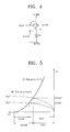
- FIG. 4 illustrates an embodiment of a pixel circuit of a display device, which, for example, may be any of the aforementioned embodiments of the display device.
- the pixel circuit includes the driving transistor M 2 and a light emitting device D 1 .
- the driving transistor M 2 may be, for example, a p-channel type. In another embodiment, the the driving transistor M 2 may have an n-channel type.
- a data voltage Data for determining the gradation of a pixel is applied to a gate electrode g of the driving transistor M 2 .
- a power supply voltage ELVDD of the light emitting device D 1 is applied to a source electrode s of the driving transistor M 2 .
- a drain electrode d of the driving transistor M 2 is connected to an anode electrode of the light emitting device D 1 .
- a power supply voltage ELVSS of the light emitting device D 1 is applied to a cathode electrode of the light emitting device D 1 .
- the light emitting device D 1 is a current driven device, luminance of the light emitting device D 1 changes in proportion to a driving current Ioled flowing into the light emitting device D 1 .
- the data voltage Data applied to the gate electrode g of the driving transistor M 2 is controlled, and a bias voltage between the power supply voltage ELVDD corresponding to a gate-source voltage Vgs of the driving transistor M 2 and the data voltage Data changes.
- the anode voltage Voled applied to the light emitting device D 1 is determined by the data voltage Data.
- FIG. 5 illustrates an example of operation points of a pixel circuit of a display device.
- first and second anode voltages Voled 1 and Voled 2 represent anode voltages applied to the light emitting device D 1 , when the driving transistor M 2 is driven at first and second gate-source voltages Vgs 1 and Vgs 2 .
- first and second driving currents Ioled 1 and Ioled 2 represent driving currents flowing into the light emitting device D 1 , when the driving transistor M 2 is driven at the first and second gate-source voltages Vgs 1 and Vgs 2 .
- the driving transistor M 2 plays a role of a voltage-to-current converting device for driving the light emitting device D 1 with a current.
- a voltage-to-current converting device for driving the light emitting device D 1 with a current.
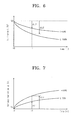
- FIG. 6 illustrates an example of relationship between passage of time and luminance degradation during operation of a display device.
- FIG. 6 is a graphing that represents a state of luminance gradation according passage of time, when a predetermined current value is provided to the light emitting device D 1 at an initial time t0 and initial luminance of the light emitting device D 1 is defined as 100%.
- luminance values that were 100% at the initial time t0 degrade, for the respective cases, by a second luminance variation ⁇ L 2 and a first luminance variation ⁇ L 1 at a first time t1 when a predetermined time passes from the initial time to.
- the amount of luminance degradation experienced by the light emitting device D 1 increases as the current value allowing the light emitting device D 1 to emit light increases.
- FIG. 7 includes a graph illustrating a relationship between the passage of time and anode voltage according to one embodiment of a display device.
- the graph illustrates an anode voltage variation according to passage of time.
- the anode voltage Va at an initial time t0 increases according to passage of time by a second voltage variation ⁇ V 2 and a first voltage variation ⁇ V 1 at time t1.
- the anode voltage increases as the current value for allowing the light emitting device D 1 to emit light increases.
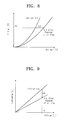
- FIG. 8 illustrates an example of change in voltage-current characteristic of a light emitting device according to time variation.
- FIG. 9 illustrates an example of a change in voltage-luminance characteristic of a light emitting device according to time variation. More specifically, in FIGS. 8 and 9 , graphs are provided which respectively illustrate changes in voltage-current characteristic (V-I) and current-luminance characteristic (I-L) of the light emitting device D 1 at initial time t0 and first time t1.
- V-I voltage-current characteristic
- I-L current-luminance characteristic
- the characteristics change according to degradation of the light emitting device D 1 .
- V-I voltage-current characteristic
- V-I voltage-current characteristic
- Ia current-luminance characteristic
- I-L current-luminance characteristic
- luminance of the light emitting device D 1 degrades according to passage of time.
- the amount of luminance degradation increases as the current for driving the light emitting device D 1 increases, and this is so even when the light emitting device D 1 is driven for the same time period.
- the amount of degradation of the light emitting device D 1 differs for different amounts of stress accumulated on the pixels 100 .
- the amount of accumulated stress may be proportional to a product of luminance of the pixel (determined, e.g., by an amount of current flowing into the light emitting device D 1 ) and time.
- the amount of accumulated stress for each pixel 100 differs, and differences in the degradation amounts of each pixel 100 occur according to a displayed pattern. Accordingly, after a predetermined time passes, an image sticking phenomenon may occur in which pixel luminance differs according to the accumulated stress amount, even though the same data voltage is applied to each pixel 100 .
- the first type of temperature effect is a temperature of the environment surrounding the display device.
- a temperature variation in the surrounding environment may change an entire temperature of the display device.
- the second type of temperature effect is local heat occurring in the display device at the time of driving the display device. For example, at the time of driving the display device, the pixels 100 are affected by local heat occurring in transistors of the pixel circuits.
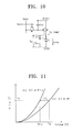
- FIG. 10 conceptually illustrates a change in anode voltage based on a pixel circuit configuration and temperature variation in one embodiment of a display device.
- the pixel circuit configuration of FIG. 10 may be the same as in FIG. 1 , except for the switch transistors M 3 and M 4 .
- drain current flowing into the driving transistor M 2 is the driving current Ioled flowing into the light emitting device D 1 .
- heat ( ⁇ (temp)) occurs in the driving transistor M 2 according to the current amount. Temperature of the light emitting device D 1 adjacent to the driving transistor M 2 increases by an effect of such heat ( ⁇ ).
- FIG. 11 illustrates a change in voltage-current characteristic of a light emitting device based on a temperature variation in accordance with one embodiment.
- V-I voltage-current characteristic of the light emitting device in a room temperature (RT) shifts towards a low voltage direction as the temperature increases by heat (a).
- a heat
- a current Ia flows into the driving transistor M 2
- a driving voltage shifts from the reference anode voltage V RT to the anode voltage V RT+ ⁇ by a voltage variation ⁇ V T .
- FIG. 12 illustrates a change in anode voltage of a light emitting device based on time and temperature in accordance with one embodiment.
- the driving current Ia is provided to the light emitting device D 1
- the anode voltages at first, second, and third times t1, t2, and t3 are affected by temperature variation of the light emitting device D 1 and are respectively measured as first, second, and third anode voltages Voled 1 , Voled 2 , and Voled 3 .
- the first, second, and third anode voltages Voled 1 , Voled 2 , and Voled 3 are compared with the reference anode voltage V RT at room temperature RT and respectively shifted by first, second, and third voltage variations ⁇ V T1 , ⁇ V T2 , and ⁇ V T3 .
- the measured anode voltage may be compensated with the reference anode voltage corresponding to the room temperature RT.
- a change in current-luminance characteristic (I-L) of the light emitting device D 1 according to a temperature variation may be much less than a change in voltage-current characteristic (V-I) according to temperature. Accordingly, the effect on the luminance of each pixel by the temperature variation may be substantially negligible.
- FIG. 13 illustrates an example of temperature dependence of an anode voltage of a light emitting device.
- the anode voltage is lowered according to an increase in temperature.
- the reference temperature is set as 25° C.
- the anode voltage represented in FIG. 13 may be expressed by Equation 1 or Equation 2.
- Voled C 1 ⁇ Temp b1 (1)
- Voled C2 ⁇ ln(Temp)+ b 2 (2)
- C1, C2, b1, and b2 are integers and changed by a driving current, a light emitting device material, and a configuration of the display device, and the like.
- C1 and C2, or, b1 and b2 may have the same value.
- the integer values C1, C2, b1, b2 are determined according to the driving current, the light emitting device material, and the configuration of the display device.
- Equations 3 and 4 temperature may be expressed by Equations 3 and 4 as functions of the anode voltage Voled.
- Temp (Voled/ C 3) 1/b3 (3)
- Temp exp ((Voled-b4)/C4) (4)
- C3, C4, b3, and b4 are integers.
- C3 and C4 have the same value and/or b3 and b4 may have the same value.
- a temperature of the light emitting device may be calculated from a difference between the measured anode voltage Voled and the already known reference anode voltage V RT at room temperature (e.g., 25° C.).
- the value of the already known reference anode voltage V RT may be a theoretical value.
- the reference anode value may be a value measured in an environment controlled at a predetermined temperature (e.g., 25° C.) before shipment from a factory.
- FIG. 14 illustrates temperature dependence of an anode voltage variation of a light emitting device according to one embodiment. More specifically, FIG. 14 represents temperature dependence of the anode voltage when a certain current I is applied to the light limiting device D 1 . Accordingly, FIG. 14 illustrates a voltage variation ⁇ V T which is a difference value between the anode voltage Voled measured at each temperature and the reference anode voltage V RT .
- the voltage variation ⁇ V T corresponds to a temperature compensation value for temperature-compensating the measured anode voltage Voled.
- a characteristic of the temperature compensation value may be expressed by Equation 5.
- ⁇ V T C 5 ⁇ ln(Temp)+ b 5 (5) where C5 and b5 are integers.
- the temperature compensation value ⁇ V T may be calculated by substituting the temperature of the light emitting device, which may be calculated by Equations 3 or 4, into Equation 5. Furthermore, the temperature compensation value ⁇ V T may be a value corresponding to the first, second, and third variation amounts ⁇ V T1 , ⁇ V T2 , ⁇ V T3 in FIGS. 11 and 12 .
- V RT Voled( t )+ ⁇ V T (6)
- an effect of the temperature variation for the light emitting device D 1 may be compensated based on Equations 1 to 6.
- an anode voltage value used for calculating the voltage variation ⁇ V is set as the reference anode voltage V RT .
- FIG. 15 illustrates a change in voltage-current-luminance characteristic of a light emitting device based on a time variation according to one embodiment.
- the voltage-current characteristic (V-I) shifts to a high voltage side based on a predetermined current value Ia, after a first time t1 passes from an initial state. Accordingly, a voltage for obtaining the current Ia increases to a voltage Vb by the voltage variation ⁇ V from an initial voltage Va.
- the current-luminance characteristic (I-L) shifts to a low luminance side after the first time t1 passes from an initial state. Accordingly, the luminance with respect to the current Ia decreases to luminance Lb by a luminance variation ⁇ L from an initial luminance La. Thus, as time passes, the voltage variation ⁇ V and luminance degradation amount ⁇ L increase.
- the necessary voltage value is Vc.
- a difference value between the initial current Ia and the current value Ic after passage of the first time t1 is a necessary current for the image sticking compensation.
- FIG. 16 illustrates a relationship between a voltage variation and a luminance variation of one embodiment of a display device.
- the luminance variation represents a luminance degradation rate when the initial luminance La is 100%.
- the luminance variation ⁇ L may be luminance degradation amount.
- the luminance degradation rate increases as the luminance degradation amount ⁇ L increases.
- the luminance amount ⁇ L increase in proportion to the voltage variation ⁇ V.
- a relationship between the voltage variation ⁇ V and the luminance amount ⁇ L may be expressed, for example, by Equation 7.
- Equation 7 the function may be changed by each RGB light emitting device material or a device structure. However, the basic relationship does not change.
- FIG. 17 illustrates an example of actually measured data and fitting data of voltage variation and luminance variation of RGB pixels of a display device.
- the curves therein represent actually measured values.
- Solid lines represent fitted ones using a function of Equation 8.
- ⁇ L C 8 ⁇ V b8 +A 8 (8) where C8, b8, and A8 are integers.
- the luminance variation represents the luminance degradation rate when the initial luminance is 100%.
- the integer A8 is a predetermined value, e.g., 100.
- Equation 8 is valid even though the material or luminance of the light emitting device D 1 is changed.
- the relationship of Equation 8 may be maintained in at least one embodiment.
- luminance degradation may be calculated based on variation of the anode voltage of each pixel 100 , from the relationship of Equation 8 between the voltage variation ⁇ V and luminance variation ⁇ L for light emitting devices D 1 having different accumulated stress amounts.
- the luminance degradation amount of the light emitting device D 1 may be determined by measuring the variation ⁇ V in anode voltage of the light emitting device D 1 using a predetermined driving current (a check current) Ia.
- the luminance degradation amount may be calculated by measuring the anode voltage variation of the light emitting device D 1 , a compensation operation corresponding to the luminance degradation amount of each pixel 100 may be performed.
- An initial anode voltage Va is measured using the check current Ia.
- the measured anode voltage Va is stored in the memory 60 as a past anode voltage Va.
- An initial state where the initial anode voltage Va is measured is a state where check is performed before shipment from a factory.
- the initial anode voltage Va may be measured under an environment controlled with a predetermined or measured room temperature RT, e.g., 25° C.
- each integer of Equations 1 to 6 may be determined, and each integer of Equations 1 to 6 may be stored in the memory 60 .
- the anode voltage Vb is measured.
- the measured anode voltage Vb is stored in the memory 60 as a current anode voltage Vb.
- temperatures of the light emitting device are respectively calculated based on Equation 3 or 4.
- the temperature compensation value ⁇ VT is calculated from the temperature calculated based on Equation 5, and past and current reference anode voltages V RT 0 and V RT 1 are obtained from the temperature compensation value ⁇ VT.
- the voltage variation ⁇ V is calculated based on the current and past reference anode voltages V RT 1 and V RT 0.
- the luminance degradation amount ⁇ L is calculated from the calculated voltage variation ⁇ V based on Equation 8.
- Each integer C8, b8, or A8 in Equation 8 may be integer data based on a predicted degradation characteristic and may be stored in the memory 60 in advance.
- the luminance degradation amount may be calculated using the foregoing method with respect to all the pixels 100 of the display device.
- the compensation current ⁇ I is calculated from the luminance degradation amount ⁇ L calculated by Equation 8.
- a current value Ic may obtain the same luminance as the initial luminance La.
- FIG. 19 illustrates a relationship between compensation current and compensation voltage of one embodiment of a display device.
- compensation voltage data ⁇ data may be calculated from a gamma characteristic in FIG. 19 , to allow the current Ioled flowing into the driving transistor M 2 to have the current value Ic.
- one embodiment of the compensation method performs compensation according to a degradation amount of each pixel 100 , by performing temperature compensation for the measured anode voltage of the light emitting device and by expressing using a predetermined function the relationship between a change amount in temperature-compensated reference anode voltage and the luminance degradation amount.
- a display device As a result, a display device, a method for calculating compensation for the display device, and a method for driving method of the display device may be provided which reduces the image sticking phenomenon and improves display quality and reliability.
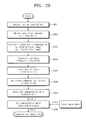
- FIG. 20 illustrates an embodiment of a method for performing compensation in a display device according.
- the anode voltage Va(t0) at the initial state is measured with the check current Ia and the measured anode voltage Va(t0) is stored in the memory 60 (operation S 201 ).
- the anode voltage Vb(t1) is measured, and the measured anode voltage Vb(t1) is stored in the memory 60 (operation S 202 ).
- a temperature Temp of the light emitting device at the time of the measurement is measured based on Equations 3 and 4
- a temperature compensation value ⁇ v T (Temp) is calculated from the calculated temperature Temp on the basis of Equation 5
- the past and the current reference anode voltages V RT 0 and V RT 1 are calculated based on Equation 6 (operation S 203 ).
- the anode voltage variation ⁇ V is calculated based on the calculated current and past reference anode voltages V RT 1 and V RT 0 (operation S 204 ).
- the luminance degradation amount ⁇ L is calculated from the calculated voltage variation ⁇ V based on Equation 8 (operation S 205 ).
- the image sticking phenomenon in the display device may be reduced and display quality and reliability may be improved.
- the data integration value 400 of the image input to the pixel is used to determine the temperature of the light emitting device D 1 .
- the data integration value may be a value where digital data is added to gradation data for each pixel of the display device.
- the data value of a display device having 8-bit gradation may have any one of values 0 to 255, wherein 0 corresponds to black and 255 corresponds to white.
- the data integration value When white is continuously displayed, the data integration value may be 255+255+255+ . . . . When black is continuously displayed, the data integration value may be 0+0+0+ . . . . When white data is input to the pixel 100 , a current value flowing into the light emitting device D 1 becomes a maximum value and heat of the driving transistor becomes large. When white data is input to the pixel 100 , current does not nearly flow into the light emitting device D 1 and the heat of the driving transistor becomes very small.
- temperature of the pixel increases as the data integration value increases.
- the relationship between the data integration value ⁇ data(t) and the pixel temperature may be expressed by Equation 11.
- Temp C 11 ⁇ data( t ) (11) where C11 denotes an integer and is changed according to a pixel configuration and a configuration of the display device.
- the integer C11 may be determined, for example, by measuring temperature dependence data of the anode voltage in the display device.
- the data integration value ⁇ data(t) corresponds to data values input to the pixels which are integrated for predetermined periods, for example, t1 to t2, and t2 to t3, . . . , as illustrated in FIG. 21 .
- the temperature Temp of the light emitting device of the pixel may be predicted, for example, using Equation 11, instead of Equations 3 and 4.
- temperature compensation may be performed, for example, using Equations 5 and 6.
- FIG. 22 illustrates another embodiment of a display device.
- the input data Idata is provided to the compensation unit 80 and the data integration unit 99 .
- the data integration unit 99 integrates data for a predetermined period, and the data integration value ⁇ data(t) is provided to the temperature compensation unit 90 .
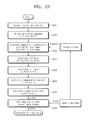
- FIG. 23 illustrates a flowchart for explaining another embodiment of a method for performing compensation in a display device.
- the anode voltage Va(t0) at the initial state is measured with the check current Ia and the measured anode voltage Va(t0) is stored in the memory 60 (operation S 231 ).
- the anode voltage Vb(t1) is measured, and the measured anode voltage Vb(t1) is stored in the memory 60 (operation S 232 ).
- the compensation current ⁇ I is calculated based on the calculated luminance degradation amount ⁇ L using Equation 9 (operation S 236 ).
- the compensation voltage data ⁇ data is calculated from the calculated compensation current ⁇ I based on the gamma characteristic illustrated in FIG. 19 (operation S 237 ).
- an image sticking phenomenon of the display device may be reduced, and display quality and reliability may be improved.
- each of the light emitting devices of a display may experience stress.
- the amount of degradation of the light emitting devices may differ based on differences in the amount of stress accumulated for each pixel.
- the amount of stress is proportional to the product of luminance (e.g., amount of current flowing into the light emitting device) and time.
- the luminance and amount of stress accumulated for each pixel may also differ for different display patterns.
- the amount of degradation experienced by each pixel may be non-uniform. Also, after a predetermined time passes, an image sticking phenomenon may occur, even though the same data voltage is applied to each pixel. As a result, the quality or reliability of the display may be degraded.
- One technique performs compensation using data integration. According to this technique, output sub-pixel data for compensation is obtained according to accumulated addition values of input sub-pixel data. A gradation greater than a typical gradation is applied to pixels having great accumulated addition values, namely, pixels expected to have great pixel degradation.
- the compensation values calculated based on data integration values may be different from actual degradation amounts of pixels. As a result, a compensation shortage or overcompensation phenomenon may occur and display quality may be degraded. Furthermore, when calculating the accumulated addition values, it is required to add by weighting each pixel in consideration of the stress amount based on input gradation data bits, not by simple integration. Accordingly, calculations become complex.
- Another technique performs compensation using luminance measurement results for dummy pixels located outside of a display area.
- the stress amounts are changed according to gradation data applied to the dummy pixels, it is difficult to completely match degradation amounts of the dummy pixels and actual pixels.
- the degradation amount for each pixel changes, a change in pixel degradation may not be completely compensated only with degradation amounts of the dummy pixels.
Landscapes
- Engineering & Computer Science (AREA)
- Physics & Mathematics (AREA)
- Computer Hardware Design (AREA)
- General Physics & Mathematics (AREA)
- Theoretical Computer Science (AREA)
- Control Of Indicators Other Than Cathode Ray Tubes (AREA)
- Control Of El Displays (AREA)
Abstract
Description
Temp=(Voled/C1)1/b1,
or
Temp=exp((Voled-b1)/C1)
where Temp is the temperature, Voled is the first voltage value and C1 and b1 are predetermined integers, and may compensate for the first voltage value based on the following equation:
ΔV T =C2·ln(Temp)+b2
where ΔVT is a temperature compensation value, Temp is temperature, and C2 and b2 are predetermined integers. The second voltage value may be a value temperature-compensated by the first compensator.
ΔL=C5·ΔV b5 +A5
where ΔL is the luminance degradation amount, ΔV is the voltage variation, and C5, b5, and A5 are predetermined integers.
ΔI=(Ia/ΔL)−Ia
where ΔI is the compensation current, ΔL is the luminance degradation amount, and Ia is a check current for measuring the voltage.
Temp=C3·Σdata(t)
where Temp is the temperature, t is a predetermined period, and where C3 is a predetermined integer, and may compensate for the first voltage value based on the following equation:
ΔV T =C4·ln(Temp)+b4
where ΔVT is the temperature compensation value to compensate for the first voltage value, Temp is the temperature, and where C4 and b4 are predetermined integers.
Temp=(Voled/C1)1/b1,
or
Temp=exp((Voled-b1)/C1)
where Temp is the temperature, Voled is the first voltage value, and C1 and b1 are predetermined integers, and compensating for the first voltage value may be performed based on the following equation:
ΔV T =C2·ln(Temp)+b2
where Temp is the temperature, ΔVT is a temperature compensation value, and C2 and b2 are predetermined integers. The second voltage value may be a value compensated based on the light emitter at a time of measuring the second voltage value.
ΔL=C5·ΔV b5 +A5
where ΔL is the luminance degradation amount, ΔV is the voltage variation, and C5, b5, and A5 are predetermined integers.
ΔI=(Ia/ΔL)−Ia
where ΔI is the compensation current, ΔL is the luminance degradation amount, and Ia is a check current for measuring the voltage.
Temp=C3·Σdata(t)
where Temp is the temperature, t is a predetermined period, and C3 is a predetermined integer, and compensating for the first voltage value may be performed based on the following equation:
ΔV T =C4·ln(Temp)+b4
where Temp is the temperature, ΔVT is the temperature compensation value to compensate for the first voltage value, and C4 and b4 are predetermined integers.
Temp=(Voled/C1)1/bl,
or
Temp=exp(Voled-b1)/C1)
where Temp is the temperature, Voled is the first voltage value, and C1 and b1 are predetermined integers, and compensating for the first voltage value may be performed based on the following equation:
ΔV T =C2·ln(Temp)+b2
where Temp is the temperature, ΔVT is a temperature compensation value, and C2 and b2 are predetermined integers. The second voltage value may be a value compensated based on the temperature of the light emitter at a time of measuring the second voltage value.
ΔL=C5·ΔV b5 +A5
where ΔL is the luminance degradation amount, ΔV is the voltage variation, and C5, b5, and A5 are predetermined integers, and the second function may include the following equation:
ΔI=(Ia/ΔL)−Ia
where ΔI is the compensation current, ΔL is the luminance degradation amount, and Ia is a check current for measuring the voltage.
Temp=C3·Σdata(t)
where Temp is the temperature, t is a predetermined period t, and C3 is predetermined integer, and compensating for the first voltage value may be performed based on the following equation:
ΔV T =C4·ln(Temp)+b4
where Temp is the temperature, ΔVT is the temperature compensation value ΔVT to compensate for the first voltage value, and C4 and b4 are predetermined integers.
Voled=C1·Tempb1 (1)
Voled=C2·ln(Temp)+b2 (2)
where C1, C2, b1, and b2 are integers and changed by a driving current, a light emitting device material, and a configuration of the display device, and the like. In one embodiment, C1 and C2, or, b1 and b2 may have the same value.
Temp=(Voled/C3)1/b3 (3)
Temp=exp((Voled-b4)/C4) (4)
where C3, C4, b3, and b4 are integers. In one embodiment, C3 and C4 have the same value and/or b3 and b4 may have the same value.
ΔV T =C5·ln(Temp)+b5 (5)
where C5 and b5 are integers.
V RT=Voled(t)+ΔV T (6)
ΔL=f(ΔV) (7)
In Equation 7, the function may be changed by each RGB light emitting device material or a device structure. However, the basic relationship does not change.
ΔL=C8·ΔV b8 +A8 (8)
where C8, b8, and A8 are integers. The luminance variation represents the luminance degradation rate when the initial luminance is 100%. The integer A8 is a predetermined value, e.g., 100.
ΔI=(Ia/ΔL)−Ia (9)
where, Ia is an initial driving current (check current).
Ic=Ia+ΔI (10)
Accordingly, the current value IC for compensation may be obtained.
Temp=C11·Σdata(t) (11)
where C11 denotes an integer and is changed according to a pixel configuration and a configuration of the display device.
Claims (20)
Temp=(Voled/C1)1/b1,
or
Temp=exp((Voled-b1)/C1)
ΔV T =C2·ln(Temp)+b2
ΔL=C5·ΔV b5 +A5
ΔI=(Ia/ΔL)−Ia
Temp=C3·Σdata(t)
ΔV T =C4·ln(Temp)+b4
Temp=(Voled/C1)1/b1,
or
Temp=exp((Voled-b1)/C1)
ΔV T =C2·ln(Temp)+b2
ΔL=C5·ΔV b5 +A5
ΔI=(Ia/ΔL)−Ia
Temp=C3·Σdata(t)
ΔV T =C4·ln(Temp)+b4
Temp=(Voled/C1)1/b1,
or
Temp=exp((Voled-b1)/C1)
ΔV T =C2·ln(Temp)+b2
ΔL=C5·ΔV b5 +A5
ΔI=(Ia/ΔL)−Ia
Temp=C3·Σdata(t)
ΔV T =C4·ln(Temp)+b4
Applications Claiming Priority (4)
| Application Number | Priority Date | Filing Date | Title |
|---|---|---|---|
| JP2013-248470 | 2013-11-29 | ||
| JP2013248470A JP2015106082A (en) | 2013-11-29 | 2013-11-29 | Display device, calculation method for compensation data of the same, and driving method for the same |
| JP2013248715A JP2015106096A (en) | 2013-11-29 | 2013-11-29 | Display device, calculation method for compensation data of the same, and driving method for the same |
| JP2013-248715 | 2013-11-29 |
Publications (2)
| Publication Number | Publication Date |
|---|---|
| US20150154910A1 US20150154910A1 (en) | 2015-06-04 |
| US9384696B2 true US9384696B2 (en) | 2016-07-05 |
Family
ID=53265811
Family Applications (1)
| Application Number | Title | Priority Date | Filing Date |
|---|---|---|---|
| US14/553,106 Active 2035-01-03 US9384696B2 (en) | 2013-11-29 | 2014-11-25 | Display device, method of calculating compensation data thereof, and driving method thereof |
Country Status (2)
| Country | Link |
|---|---|
| US (1) | US9384696B2 (en) |
| KR (1) | KR102215204B1 (en) |
Cited By (3)
| Publication number | Priority date | Publication date | Assignee | Title |
|---|---|---|---|---|
| US20160276038A1 (en) * | 2015-03-17 | 2016-09-22 | Renesas Electronics Corporation | Semiconductor device |
| US11049444B2 (en) | 2019-03-28 | 2021-06-29 | Samsung Display Co., Ltd. | Display device and driving method thereof |
| US11264445B2 (en) * | 2019-07-23 | 2022-03-01 | Samsung Display Co., Ltd. | Method of compensating for degradation of display device |
Families Citing this family (20)
| Publication number | Priority date | Publication date | Assignee | Title |
|---|---|---|---|---|
| TWI600000B (en) * | 2013-05-23 | 2017-09-21 | Joled Inc | Image signal processing circuit, image signal processing method and display device |
| KR102280095B1 (en) * | 2015-06-30 | 2021-07-20 | 엘지디스플레이 주식회사 | Organic light emitting diode display device and method for driving the same |
| KR102279397B1 (en) * | 2015-06-30 | 2021-07-19 | 엘지디스플레이 주식회사 | Organic light emitting display device and driving method thereof |
| KR102387787B1 (en) * | 2015-08-24 | 2022-04-15 | 엘지디스플레이 주식회사 | Organic light emitting diode display device and method for driving the same |
| KR102537608B1 (en) | 2016-01-28 | 2023-05-30 | 삼성디스플레이 주식회사 | Display device and method for displaying image thereof |
| KR102494156B1 (en) * | 2016-06-28 | 2023-02-01 | 엘지디스플레이 주식회사 | Organic Light Emitting Display Device And Image Data Correction Method Thereof |
| KR102581368B1 (en) | 2016-07-07 | 2023-09-22 | 삼성디스플레이 주식회사 | Method of driving display panel and display apparatus for performing the same |
| US11282449B2 (en) * | 2016-09-22 | 2022-03-22 | Apple Inc. | Display panel adjustment from temperature prediction |
| US10453432B2 (en) * | 2016-09-24 | 2019-10-22 | Apple Inc. | Display adjustment |
| US11380260B2 (en) * | 2017-04-07 | 2022-07-05 | Apple Inc. | Device and method for panel conditioning |
| CN106960656B (en) | 2017-05-11 | 2019-03-19 | 京东方科技集团股份有限公司 | A kind of organic light emitting display panel and its display methods |
| US10642083B1 (en) * | 2017-05-26 | 2020-05-05 | Apple Inc. | Predictive temperature compensation |
| CN107799069B (en) * | 2017-11-17 | 2019-08-30 | 京东方科技集团股份有限公司 | Pixel compensation system, drive system and method, time-sequence control module, device |
| US10755783B2 (en) | 2018-08-27 | 2020-08-25 | Silicon Storage Technology | Temperature and leakage compensation for memory cells in an analog neural memory system used in a deep learning neural network |
| KR102571750B1 (en) * | 2018-10-04 | 2023-08-28 | 삼성디스플레이 주식회사 | Display device and method for displaying image using display device |
| CN109493805B (en) * | 2018-12-12 | 2021-04-27 | 合肥鑫晟光电科技有限公司 | Compensation method and device of display panel |
| KR102648198B1 (en) | 2019-01-14 | 2024-03-19 | 삼성디스플레이 주식회사 | Afterimage compensator and display device having the same |
| US11295334B2 (en) * | 2019-04-30 | 2022-04-05 | Bank Of America Corporation | Batch transaction multiplexing engine |
| US20230136688A1 (en) * | 2021-10-29 | 2023-05-04 | Ignis Innovation Inc. | High efficiency stress history modelling and compensation |
| CN116543689A (en) * | 2023-03-30 | 2023-08-04 | 天马新型显示技术研究院(厦门)有限公司 | Display panel, driving method thereof and display device |
Citations (10)
| Publication number | Priority date | Publication date | Assignee | Title |
|---|---|---|---|---|
| US20050110720A1 (en) * | 2003-11-21 | 2005-05-26 | Hitachi Displays, Ltd. | Image display device |
| JP2005275182A (en) | 2004-03-26 | 2005-10-06 | Sony Corp | Image persistence correction device, display device, image processor, program, and recording medium |
| US20060033452A1 (en) * | 2004-08-13 | 2006-02-16 | Shunpei Yamazaki | Light emitting device using light emitting element and driving method of light emitting element, and lighting apparatus |
| JP2007187761A (en) | 2006-01-11 | 2007-07-26 | Sony Corp | Self-luminous display, estimated degradation information correction device, input display data correction device, and program |
| US20080042943A1 (en) | 2006-06-16 | 2008-02-21 | Cok Ronald S | Method and apparatus for averaged luminance and uniformity correction in an am-el display |
| JP2008185670A (en) | 2007-01-29 | 2008-08-14 | Sony Corp | Organic electroluminescence display device, control method of organic electroluminescence display device, and electronic equipment |
| JP2009098433A (en) | 2007-10-17 | 2009-05-07 | Canon Inc | Display and its driving method |
| JP2010500620A (en) | 2006-08-15 | 2010-01-07 | イグニス・イノベイション・インコーポレーテッド | OLED brightness degradation compensation |
| JP2010091703A (en) | 2008-10-07 | 2010-04-22 | Sony Corp | Display apparatus |
| EP2126883B1 (en) | 2007-01-24 | 2012-01-25 | Global OLED Technology LLC | Oled display with aging and efficiency compensation |
Family Cites Families (4)
| Publication number | Priority date | Publication date | Assignee | Title |
|---|---|---|---|---|
| KR100505342B1 (en) * | 1999-12-30 | 2005-08-04 | 고등기술연구원연구조합 | Apparatus for measuring life time of organic electroluminescence device |
| US7079091B2 (en) * | 2003-01-14 | 2006-07-18 | Eastman Kodak Company | Compensating for aging in OLED devices |
| KR100902238B1 (en) * | 2008-01-18 | 2009-06-11 | 삼성모바일디스플레이주식회사 | Organic light emitting display and driving method thereof |
| KR100902245B1 (en) * | 2008-01-18 | 2009-06-11 | 삼성모바일디스플레이주식회사 | Organic light emitting display and driving method thereof |
-
2014
- 2014-11-24 KR KR1020140164586A patent/KR102215204B1/en active IP Right Grant
- 2014-11-25 US US14/553,106 patent/US9384696B2/en active Active
Patent Citations (10)
| Publication number | Priority date | Publication date | Assignee | Title |
|---|---|---|---|---|
| US20050110720A1 (en) * | 2003-11-21 | 2005-05-26 | Hitachi Displays, Ltd. | Image display device |
| JP2005275182A (en) | 2004-03-26 | 2005-10-06 | Sony Corp | Image persistence correction device, display device, image processor, program, and recording medium |
| US20060033452A1 (en) * | 2004-08-13 | 2006-02-16 | Shunpei Yamazaki | Light emitting device using light emitting element and driving method of light emitting element, and lighting apparatus |
| JP2007187761A (en) | 2006-01-11 | 2007-07-26 | Sony Corp | Self-luminous display, estimated degradation information correction device, input display data correction device, and program |
| US20080042943A1 (en) | 2006-06-16 | 2008-02-21 | Cok Ronald S | Method and apparatus for averaged luminance and uniformity correction in an am-el display |
| JP2010500620A (en) | 2006-08-15 | 2010-01-07 | イグニス・イノベイション・インコーポレーテッド | OLED brightness degradation compensation |
| EP2126883B1 (en) | 2007-01-24 | 2012-01-25 | Global OLED Technology LLC | Oled display with aging and efficiency compensation |
| JP2008185670A (en) | 2007-01-29 | 2008-08-14 | Sony Corp | Organic electroluminescence display device, control method of organic electroluminescence display device, and electronic equipment |
| JP2009098433A (en) | 2007-10-17 | 2009-05-07 | Canon Inc | Display and its driving method |
| JP2010091703A (en) | 2008-10-07 | 2010-04-22 | Sony Corp | Display apparatus |
Cited By (5)
| Publication number | Priority date | Publication date | Assignee | Title |
|---|---|---|---|---|
| US20160276038A1 (en) * | 2015-03-17 | 2016-09-22 | Renesas Electronics Corporation | Semiconductor device |
| US9570188B2 (en) * | 2015-03-17 | 2017-02-14 | Renesas Electronics Corporation | Semiconductor device |
| US11049444B2 (en) | 2019-03-28 | 2021-06-29 | Samsung Display Co., Ltd. | Display device and driving method thereof |
| US11264445B2 (en) * | 2019-07-23 | 2022-03-01 | Samsung Display Co., Ltd. | Method of compensating for degradation of display device |
| US11665941B2 (en) | 2019-07-23 | 2023-05-30 | Samsung Display Co., Ltd. | Method of compensating for degradation of display device |
Also Published As
| Publication number | Publication date |
|---|---|
| KR20150062968A (en) | 2015-06-08 |
| US20150154910A1 (en) | 2015-06-04 |
| KR102215204B1 (en) | 2021-02-16 |
Similar Documents
| Publication | Publication Date | Title |
|---|---|---|
| US9384696B2 (en) | Display device, method of calculating compensation data thereof, and driving method thereof | |
| US10304385B2 (en) | Display device | |
| TWI598866B (en) | A data processing device for a display device, a data processing method for the display device and the display device | |
| US8269803B2 (en) | Display device and method for driving the same | |
| US8830148B2 (en) | Organic electroluminescence display device and organic electroluminescence display device manufacturing method | |
| US9679516B2 (en) | Organic light emitting display and method for driving the same | |
| KR101920169B1 (en) | Display device and drive method for same | |
| KR101419450B1 (en) | Electroluminescent Display with Compensation of Efficiency Variations | |
| JP5443504B2 (en) | Method for providing drive transistor control signal to drive transistor | |
| KR102212424B1 (en) | Display deviceand driving method thereof | |
| US20150213757A1 (en) | Display device and method for driving the same | |
| KR102028504B1 (en) | Organic light-emtting diode display device incuding compensation circuit | |
| CN113853645B (en) | Display device and driving method thereof | |
| KR20140014694A (en) | Apparatus and method for compensating of image in display device | |
| KR102084711B1 (en) | Display deviceand driving method thereof | |
| KR20100086876A (en) | Display device and driving method thereof | |
| KR20140014671A (en) | Display device and driving method of the same | |
| KR20160055559A (en) | Organic Light Emitting Display Device and Driving Method Thereof | |
| CN112820239A (en) | Display device and driving method of display device | |
| KR20190078316A (en) | Organic Light Emitting Display Device and Method for Driving the Same | |
| KR102535821B1 (en) | Display device and method opereation thereof | |
| JP2015106096A (en) | Display device, calculation method for compensation data of the same, and driving method for the same | |
| JP2016090940A (en) | Display device, display method and program | |
| KR102183824B1 (en) | Organic light emitting display device | |
| JP2015106082A (en) | Display device, calculation method for compensation data of the same, and driving method for the same |
Legal Events
| Date | Code | Title | Description |
|---|---|---|---|
| AS | Assignment |
Owner name: SAMSUNG DISPLAY CO., LTD., KOREA, REPUBLIC OF Free format text: ASSIGNMENT OF ASSIGNORS INTEREST;ASSIGNORS:OKUNO, TAKESHI;MORIMOTO, KAZUNORI;KOMIYA, NAOAKI;REEL/FRAME:034262/0166 Effective date: 20141120 |
|
| FEPP | Fee payment procedure |
Free format text: PAYOR NUMBER ASSIGNED (ORIGINAL EVENT CODE: ASPN); ENTITY STATUS OF PATENT OWNER: LARGE ENTITY |
|
| STCF | Information on status: patent grant |
Free format text: PATENTED CASE |
|
| MAFP | Maintenance fee payment |
Free format text: PAYMENT OF MAINTENANCE FEE, 4TH YEAR, LARGE ENTITY (ORIGINAL EVENT CODE: M1551); ENTITY STATUS OF PATENT OWNER: LARGE ENTITY Year of fee payment: 4 |
|
| FEPP | Fee payment procedure |
Free format text: MAINTENANCE FEE REMINDER MAILED (ORIGINAL EVENT CODE: REM.); ENTITY STATUS OF PATENT OWNER: LARGE ENTITY |