US9341852B2 - Cell substrate inspection system and method - Google Patents
Cell substrate inspection system and method Download PDFInfo
- Publication number
- US9341852B2 US9341852B2 US13/214,383 US201113214383A US9341852B2 US 9341852 B2 US9341852 B2 US 9341852B2 US 201113214383 A US201113214383 A US 201113214383A US 9341852 B2 US9341852 B2 US 9341852B2
- Authority
- US
- United States
- Prior art keywords
- cell substrate
- parallax
- image
- parallax image
- lenticular lens
- Prior art date
- Legal status (The legal status is an assumption and is not a legal conclusion. Google has not performed a legal analysis and makes no representation as to the accuracy of the status listed.)
- Expired - Fee Related, expires
Links
- 239000000758 substrate Substances 0.000 title claims abstract description 286
- 238000007689 inspection Methods 0.000 title claims abstract description 65
- 238000000034 method Methods 0.000 title claims description 45
- 238000012360 testing method Methods 0.000 claims abstract description 50
- 238000003384 imaging method Methods 0.000 claims abstract description 29
- 230000007547 defect Effects 0.000 claims description 110
- 230000002950 deficient Effects 0.000 description 41
- 238000004519 manufacturing process Methods 0.000 description 20
- 230000008569 process Effects 0.000 description 14
- 230000004888 barrier function Effects 0.000 description 8
- 239000011521 glass Substances 0.000 description 8
- 239000000853 adhesive Substances 0.000 description 5
- 230000001070 adhesive effect Effects 0.000 description 5
- 239000004973 liquid crystal related substance Substances 0.000 description 5
- 239000011159 matrix material Substances 0.000 description 3
- 230000001681 protective effect Effects 0.000 description 3
- 238000004458 analytical method Methods 0.000 description 2
- 230000008901 benefit Effects 0.000 description 2
- 238000010586 diagram Methods 0.000 description 2
- 230000000694 effects Effects 0.000 description 2
- 238000005401 electroluminescence Methods 0.000 description 2
- 238000005452 bending Methods 0.000 description 1
- 230000008859 change Effects 0.000 description 1
- 238000006073 displacement reaction Methods 0.000 description 1
- 239000000284 extract Substances 0.000 description 1
- 238000010348 incorporation Methods 0.000 description 1
- 238000012986 modification Methods 0.000 description 1
- 230000004048 modification Effects 0.000 description 1
- 230000003287 optical effect Effects 0.000 description 1
- 230000010287 polarization Effects 0.000 description 1
- 238000012545 processing Methods 0.000 description 1
- 239000011347 resin Substances 0.000 description 1
- 229920005989 resin Polymers 0.000 description 1
- 238000006748 scratching Methods 0.000 description 1
- 230000002393 scratching effect Effects 0.000 description 1
- 238000006467 substitution reaction Methods 0.000 description 1
Images


Classifications
-
- G02B27/2214—
-
- G—PHYSICS
- G02—OPTICS
- G02B—OPTICAL ELEMENTS, SYSTEMS OR APPARATUS
- G02B30/00—Optical systems or apparatus for producing three-dimensional [3D] effects, e.g. stereoscopic images
- G02B30/20—Optical systems or apparatus for producing three-dimensional [3D] effects, e.g. stereoscopic images by providing first and second parallax images to an observer's left and right eyes
- G02B30/26—Optical systems or apparatus for producing three-dimensional [3D] effects, e.g. stereoscopic images by providing first and second parallax images to an observer's left and right eyes of the autostereoscopic type
- G02B30/27—Optical systems or apparatus for producing three-dimensional [3D] effects, e.g. stereoscopic images by providing first and second parallax images to an observer's left and right eyes of the autostereoscopic type involving lenticular arrays
-
- G—PHYSICS
- G01—MEASURING; TESTING
- G01N—INVESTIGATING OR ANALYSING MATERIALS BY DETERMINING THEIR CHEMICAL OR PHYSICAL PROPERTIES
- G01N21/00—Investigating or analysing materials by the use of optical means, i.e. using sub-millimetre waves, infrared, visible or ultraviolet light
- G01N21/84—Systems specially adapted for particular applications
- G01N21/88—Investigating the presence of flaws or contamination
- G01N21/95—Investigating the presence of flaws or contamination characterised by the material or shape of the object to be examined
- G01N2021/9513—Liquid crystal panels
Definitions
- Embodiments described herein relate generally to the inspection system and the method of the cell substrate used for a three-dimensional image display apparatus.
- integral-imaging 3D image display apparatuses In recent years, three-dimensional image display apparatuses not requiring special glasses are being developed. For example, some integral-imaging 3D image display apparatuses have been developed, in which images taken in plural directions are shown according to the viewing angles to provide a stereoscopic image.
- the integral-imaging system has a plurality of parallax images and therefore provides motion parallax, in which the image seen by a viewer changes as the viewing point of the viewer moves.
- Each integral-imaging 3D image display apparatus is manufactured by bonding a lenticular lens to a planer display substrate such as a liquid crystal panel (hereinafter, referred to as a cell substrate).
- a cell substrate such as a liquid crystal panel
- the influence of defects caused in the cell substrate on each parallax image of the stereoscopic image can be checked by a lighting test which displays an image after the lenticular lens is bonded to the cell substrate.
- each parallax image looks when the cell substrate is defective until the cell substrate is bonded to the lenticular lens. If the cell substrate is defective, the lenticular lens needs to be separated from the cell substrate. In many integral imaging 3D image display apparatuses, the cell substrate and lenticular lens are bonded to each other with an adhesive. Accordingly, it is difficult or impossible to separate the lenticular lens from the cell substrate. If the lenticular lens cannot be separated, the cell substrate and lenticular lens are both disposed of.
- the method of inspecting a cell substrate for defects after bonding the lenticular lens to the cell substrate requires high manufacturing cost and long manufacturing time.
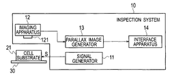
- FIG. 1 is a schematic block diagram showing a configuration of an inspection system according to a first embodiment.
- FIG. 2 is a cross-sectional view schematically showing an example of a three-dimensional image display apparatus.
- FIG. 3 is a top view schematically showing a display region of a cell substrate of the three-dimensional image display apparatus shown in FIG. 2 .
- FIG. 4 is a schematic view showing a principle of stereoscopic display by the three-dimensional image display apparatus shown in FIG. 2 .
- FIG. 5 is a top view schematically showing an example of a cell substrate having a defect in the display region.
- FIGS. 6A to 6I are schematic views showing examples of parallax image predictions generated by the inspection system according to the first embodiment.
- FIG. 7 is a flowchart for explaining an inspection method by the inspection system according to the first embodiment.
- FIG. 8 is a top view schematically showing an example of defects caused in the cell substrate.
- FIG. 9 is a top view schematically showing another example of defects caused in the cell substrate.
- FIGS. 10A and 10B are schematic views illustrating a method of manufacturing a three-dimensional image display apparatus using the result of inspection of a cell substrate.
- FIG. 11 is a schematic block diagram showing a configuration of an inspection system according to a second embodiment.
- FIG. 12 is a flowchart for explaining an inspection method by the inspection system according to the second embodiment.
- a system for inspecting a cell substrate which is bonded to a lenticular lens for use in an integral-imaging three-dimensional image display apparatus and includes a display region composed of an array of a plurality of sub-regions, each sub-region displaying a set of parallax image information obtained by dividing each of a plurality of parallax images, is provided.
- the above inspection system includes: a signal generator transmitting to a cell substrate as an inspection object, a display signal causing the cell substrate to display a test image; an imaging apparatus capturing the test image displayed on the cell substrate receiving the display signal; a parallax image generator arranging the set of parallax image information of the captured test image for each parallax image in order to generate a parallax image prediction of parallax image which is obtained when the cell substrate is bonded to the lenticular lens; and an interface apparatus displaying the parallax image predictions.
- a cell substrate inspection system 10 is a system of inspecting a cell substrate 21 for use in an integral-imaging 3D image display apparatus.
- the cell substrate 21 is a planar display substrate which is bonded to a lenticular lens for use and, as later described, includes a display region composed of an array of plural sub-regions. Each sub-region displays parallax image information obtained by dividing each of plural parallax images.
- the inspection system 10 includes a signal generator 11 , an imaging apparatus 12 , a parallax image generator 13 , and an interface apparatus 14 .
- the signal generator 11 sends a display signal S causing the cell substrate 21 as an inspection object, to display a test image.
- the imaging apparatus 12 captures an image of the test image displayed on the cell substrate 21 receiving the display signal S.
- the parallax image generator 13 generates a parallax image prediction of each parallax image which can be obtained when the cell substrate 21 is bonded to a lenticular lens by arranging sets of parallax image information of the captured test image for each parallax image.
- the interface apparatus 14 displays the parallax image predictions.
- the 3D image display apparatus 20 has a structure in which the cell substrate 21 displaying images is bonded to a lens plate 22 including a lenticular lens 221 with an adhesive 23 .
- the cell substrate 21 includes a laminate structure of first and second substrates 212 and 213 . Within the cell substrate 21 , plural pixels are arranged in a predetermined pattern, for example, in a matrix fashion. First and second polarization plates 211 and 214 are provided outside of the first and second substrate 212 and 213 , respectively, so as to be opposed to each other.
- the first substrate 212 is a rectangular glass substrate, for example.
- a plurality of pixel electrodes (not shown), electrical wires for setting potentials of the pixel electrodes (not shown), and the like are arranged.
- the pixel electrodes are arranged in a dot fashion in each pixel, and the electrical wires are arranged in a matrix fashion.
- the second substrate 213 is a rectangular glass substrate, for example.
- a color filter F In the surface of the second substrate 213 facing the first substrate 212 , a color filter F, a counter electrode as a common electrode (not shown), and the like are arranged.
- the color filter F is composed of plural color layers (for example, red, green, and blue layers) arranged in a dotted or a striped fashion and a light shielding layer such as a black matrix.
- the cell substrate 21 is a liquid crystal panel, a not-shown backlight is provided under the cell substrate 21 .
- the lens plate 22 has a structure including a protective glass 222 and a lenticular lens 221 which are laid on each other.
- the lenticular lens 221 includes plural cylindrical lenses side by side in a direction (in a short-side direction) perpendicular to the axial direction (the longitudinal direction, or the ridge line direction) thereof. Each cylindrical lens has a shape obtained by dividing a column into two in the axial direction.
- the cylindrical lens has a curvature on one side and includes one light bending surface.
- the lenticular lens 221 includes plural barrel-shaped cylindrical lenses arranged side by side, and curve surfaces T of the cylindrical lenses face the cell substrate 21 .
- Light emitted from the display region of the cell substrate 21 is incident to the lenticular lens 221 through the curve surfaces T, then passes through the lenticular lens 221 and protective glass 222 , and then outputted to the outside of the 3D image display apparatus 20 .
- the adhesive 23 is provided between the second substrate 213 and protective glass 222 around the lenticular lens 221 to bond the cell substrate 21 and lens plate 22 .
- the adhesive 23 is formed between the cell substrate 21 and lens plate 22 into a rectangular frame shape, for example.
- the adhesive 23 can be light curing resin.
- FIG. 3 shows an example of the display region of the cell substrate 21 when the number of parallax images is nine.
- the display region of the cell substrate 21 is divided into sub-regions displaying the nine parallax images 0 to 8 .
- the number of parallax images is not limited to nine.
- the display region of the cell substrate 21 is divided into stripe sub-regions a 0 to a 8 , b 0 to b 8 . . . extending in a column direction.
- Each of the sub-regions a 0 , b 0 . . . displays parallax image information of each portion obtained by dividing the parallax image 0 .
- the sub-regions a 1 , b 1 . . . display parallax image information of each portion obtained by dividing the parallax image 1 .
- sets of parallax image information of the portions of the parallax images 2 to 8 are displayed in the sub-regions a 2 , b 2 . .
- the sets of parallax image information of the parallax images 0 to 8 are displayed side by side in turn in the row direction.
- FIG. 4 shows the principle of stereoscopic display by the 3D image display apparatus 20 shown in FIG. 2 .
- Rays of light emitted from the display region of the cell substrate 21 are radiated by the lenticular lens 221 in predetermined directions defined for the individual parallax images.
- arrows L 0 to L 8 indicate directions of the sets of parallax image information of the parallax images 0 to 8 radiated from the cell substrate 21 , respectively.
- the sets of parallax image information of the parallax image 0 radiated in the same direction are arranged side by side to form the parallax image 0 .
- the sets of parallax image information of the parallax images 1 to 8 are arranged side by side for each parallax image to form the parallax images 1 to 8 , respectively.
- the 3D image display apparatus 20 uses the cell substrate 21 and lenticular lens 221 to display plural parallax images (two-dimensional images), which look in a little different ways depending on the viewing angles, thus forming a 3D image.
- the 3D image display apparatus 20 displays a stereoscopic image by displaying parallax images taken in the plural directions according to the viewing angles.
- the cell substrate 21 is inspected for the presence of bright and dark dot defects, linear defects, display unevenness, and the like.
- the bright dot defect refers to a dot always bright in the display region of the cell substrate 21 independent of the display signal S prescribing the display image on the cell substrate 21
- the dark dot defect is a dot always dark in a similar manner.
- the linear defect includes bright or dark dots successively located from end to end of the display region. As for the bright and dark dot defects, the presence of a bright or dark dot defect solely caused does not always result in determination that the cell substrate 21 is defective.
- a successive dark dot defect including plural dark dots successively located or a successive bright dot defect including plural bright dot defects successively located it is defined how many dark or bright dot defects are considered as a successive dark or bright dot defect which is an object determined to be defective. Furthermore, it is defined by how many defined successive dark or bright dot defects the cell substrate 21 is determined to be defective.
- the aforementioned criteria are set to determine whether the cell substrate 21 is a non-defective product. This is because even if there is one independent dark or bright dot defect, the viewer of the display image of the 3D image display apparatus 20 often does not notice the dark or bright dot defect or are not bothered by the same.
- the cell substrate 21 including a dark or bright dot defect can be shipped as a non-defective product in some cases.
- the cell substrate 21 If the cell substrate 21 is defective, it is necessary to examine how each parallax image looks. It is not proper that the quality of the cell substrate 21 is determined only by the results of inspection for dark or bright dot defects in the display region of the cell substrate 21 . This is because inspection for dark or bright dot defects is necessary for each parallax image obtained through the lenticular lens 221 bonded to the cell substrate 21 . In other words, it is necessary to know the influence of defects of the cell substrate 21 on each parallax image.
- the parallax image generator 13 predicts parallax images which could be obtained by arranging the sets of parallax image information of the test image side by side when the cell substrate 21 is bonded to the lenticular lens 221 .
- the test image captured by the imaging apparatus 12 includes the sets of parallax image information of each parallax image which are arranged in turn.
- the parallax image generator 13 extracts the regions corresponding to each viewing point from the captured test image to generate a parallax image prediction of each parallax image.
- every n-th sub-regions (n is the number of parallax images) are extracted from the display region of the cell substrate 21 , and the sets of parallax image information displayed in the extracted sub-regions are then arranged side by side to generate a parallax image prediction of each parallax image.
- the test image includes the parallax images 0 to 8
- the sets of parallax image information displayed in every n-th sub-regions extracted from the display region of the cell substrate 21 are arranged to generate parallax image predictions 0 p to 8 p of the parallax images 0 to 8 .
- FIG. 5 shows an example in which a defect D including a series of dark dot defects from the sub-region m 3 to the sub-region m 6 in the cell substrate 21 .
- FIGS. 6A to 6I show the parallax image predictions 0 p to 8 p of the parallax images 0 to 8 which will be obtained when the cell substrate 21 shown in FIG. 5 is bonded to the lenticular lens 221 .
- the parallax image predictions 0 p to 8 p are obtained by arranging the sets of parallax image information of each parallax image of the test image side by side.
- the defect D of the cell substrate 21 shown in FIG. 5 is caused in the regions m 3 to m 6 which display part of the parallax image information of the parallax images 3 to 6 , respectively. Accordingly, as shown in FIG.
- the parallax image predictions 3 p to 6 p includes defects D 3 to D 6 , respectively. According to the inspection system 10 shown in FIG. 1 , it is therefore possible to know the influence of defects included in the cell substrate 21 on each parallax image.
- step S 10 of FIG. 7 the cell substrate 21 to be inspected is placed on a stage 30 .
- step S 20 the signal generator 11 generates the display signal S causing the cell substrate 21 to display a test image.
- the cell substrate 21 receives the display signal S and displays the test image.
- the signal generator 11 sends to the cell substrate 21 the display signal S causing all the pixels to have maximum brightness.
- the display region of the cell substrate 21 is visually observed as a white screen although zooming-in shows that each R, G, or B pixel has the maximum brightness.
- the signal generator 11 sends to the cell substrate 21 the display signal S causing all the pixels to have the minimum brightness.
- step S 30 the imaging apparatus 12 captures the test image displayed on the cell substrate 21 .
- the optical system including the imaging apparatus 12 and an imaging lens 121 used in the imaging apparatus 12 needs a resolution high enough to determine the state of each R, G, or B pixel (hereinafter, referred to as a sub-pixel). If the states of all the sub-pixels of the cell substrate 21 cannot be determined by one shot due to the relation between the resolution of the imaging apparatus 12 and the number of pixels of the cell substrate 21 , it is possible to capture the test image several times while moving a smaller imaging range.
- a number of the parallax image of which the parallax image prediction is generated at first is set to 1.
- step S 50 the parallax image generator 13 performs data processing for the captured image of the test image to generate a parallax image prediction of the number n.
- the sets of parallax image information of the parallax image No. n included in the test image are arranged side by side to generate a parallax image prediction.
- the generated parallax image prediction is displayed on the interface apparatus 14 .
- step S 60 an operator who is using the inspection system 10 observes the parallax image predictions displayed on the interface apparatus 14 and determines the presence of a defect in each parallax image based on the parallax image predictions. Specifically, the operator determines the quality of the cell substrate 21 based on the number of dark or bright dot defects in a successive dark or bright dot defect which is defined as an object for quality determination of the cell substrate 21 and the allowable number of successive dark or bright dot defects. For example, it is assumed that a successive dark or bright dot defect including three or more dark or bright dot defects is defined as a defect which is an object for the quality determination of the cell substrate 21 .
- the cell substrate 21 is determined to be a defective if the number of successive dark or bright dot defects is greater than the allowable number. Furthermore, the quality of the cell substrate 21 may be determined based on the presence of a linear defect or display unevenness.
- step S 70 based on the observation of the parallax image predictions, the operator records the presence of a defect in the cell substrate 21 . For example, the operator inputs the presence of a defect in the cell substrate 21 to the interface apparatus 14 . The information inputted to the interface apparatus 14 is recorded in the inspection system 10 as a determination result. If the cell substrate 21 includes a defect in the step S 80 , the process proceeds to step S 90 , and the operator records the detail of the defect.
- step S 100 the interface apparatus 14 displays that the cell substrate 21 is determined to be a defective and the detail of the defect. The process is then terminated. vii) On the other hand, if the cell substrate 21 is not defective in the step S 80 , the process proceeds to step S 110 , in which it is determined whether all of the parallax images of the cell substrate 21 are already inspected. If all of the parallax images are not yet inspected, in the step S 120 , the number n of the parallax image to be predicted is incremented by 1, and the process returns to the step S 50 .
- the process proceeds to step S 130 , and the interface apparatus 14 displays that the cell substrate 21 is determined to be a non-defective product.
- the cell substrate 21 is determined to be defective without performing the inspection for defects in the parallax images not yet inspected, and the process is terminated.
- a defective cell substrate 21 can be used to manufacture the three-dimensional image display apparatus 20 in some cases depending on the position of the defect in the cell substrate 21 and the quality criteria. Accordingly, all of the parallax images of the cell substrate 21 may be inspected independently of the presence of a defect in each parallax image before the process is terminated.
- the way of outputting the result of the quality determination can be displaying the results on various types of display apparatuses, outputting the results through a printer, or recording the results in a database integrally managing quality data of the cell substrate 21 .
- the result of quality determination of the cell substrate 21 is inputted to the interface apparatus 14 and is then transmitted from the inspection system 10 to the database.
- the method of clarifying sub-pixels of a parallax image of which the parallax image prediction is to be generated can be, in addition to the method of simultaneously displaying all the parallax images on the cell substrate 21 , a method of displaying a test image including only one selected from the plural parallax images. For example, it is possible to display only pixels of a particular parallax image with a determination brightness while displaying pixels of the other parallax images with a brightness different from the determination brightness. In the inspection for dark dot defects, only the sub-pixels of a parallax image wanted to be predicted are displayed with the maximum brightness while the sub-pixels of the other parallax images are displayed with the minimum brightness.
- the aforementioned method of displaying the test image including only a particular parallax image is also effective when the parallax image cannot be specified if all the parallax images are simultaneously displayed.
- the parallax image is specified by how many sub-regions there are before the referential position of the cell substrate 21 (for example, the left end of the display region)
- the referential position can be misidentified, preventing precise specification of the parallax image.
- the parallax images are sequentially inspected one by one, it is possible to precisely recognize which place is influenced by defects caused in the cell substrate 21 .
- the positions of sub-pixels cannot be specified in some cases due to little light emitted from good sub-pixels.
- the positions of sub-pixels in the imaging range of the imaging apparatus 12 are recorded in advance using a maximum brightness image for the dark dot inspection.
- the maximum brightness image with each R, G, or B pixel of the cell substrate 21 having the maximum brightness is captured by the imaging apparatus 12 , and each position of the sub-pixels at this time is recorded.
- the test image for the bright dot inspection is displayed on the cell substrate 21 and is then captured. Comparing the recorded positions of the sub-pixels with the captured test image, the positions of sub-pixels in the test image can be specified.
- the inspection method of the first embodiment it is possible to perform inspections for successive dark or bright dot defects of each parallax image after the process of bonding the cell substrate 21 to the lenticular lens 221 .
- the whole 3D image display apparatus 20 including the lenticular lens 221 should be disposed of.
- the 3D image display apparatus 20 is dissembled, and only the cell substrate 21 is disposed of.
- the lenticular lens 221 is bonded to another cell substrate 21 again.
- this will increase the manufacturing cost and time of the 3D image display apparatus 20 .
- the substrate 21 can be solely inspected for successive dark or bright dot defects in each parallax image before the process of bonding the cell substrate 21 to the lenticular lens 221 . This can prevent the manufacturing cost and time of the 3D image display apparatus 20 from increasing.
- the inspection system 10 of the first embodiment based on the display image on the cell substrate 21 before the cell substrate 21 is bonded to the lenticular lens 21 , it is predicted how each parallax image looks when the cell substrate 21 is bonded to the lenticular lens 21 .
- the presence of a defect in the cell substrate 21 influencing each parallax image can be examined before the cell substrate 21 is bonded to the lenticular lens 221 . It is therefore possible to provide the inspection system and method which detect defects in the cell substrate 21 for use in the 3D image display apparatus 20 while preventing the manufacturing cost and time thereof from increasing.
- the cell substrate 21 which is determined to be defective for the 3D image display apparatus 20 using a certain number of parallax images can be applied to another 3D image display apparatus 20 using a different number of parallax images without any problem.
- the number of parallax images of the 3D image display apparatus 20 to which the defective cell substrate 21 can be applied as a non-defective product can be determined based on the result of inspection of the cell substrate 21 , thus manufacturing the 3D image display apparatus 20 .
- the cell substrate 21 shown in FIG. 8 it is assumed that a defect D is caused successively from the region m 0 to the region m 8 in the cell substrate 21 .
- the defective regions m 0 and m 7 are included in a same parallax image (the parallax image 0 )
- the defective regions m 1 and m 8 are included in a same parallax image (the parallax image 1 ).
- the parallax images 0 and 1 the defective sets of parallax image information are located side by side.
- the quality criteria of the cell substrate 21 are defined so that the cell substrate 21 is determined to be defective when the cell substrate 21 includes two or more successive dark or bright dot defects, the cell substrate 21 shown in FIG. 8 is determined to be defective.
- each of the parallax images includes each defect due to the defect D of the cell substrate 21 shown in FIG. 8 but does not include successive defects. Accordingly, the cell substrate 21 shown in FIG. 8 is determined to be a non-defective.
- the cell substrate 21 shown in FIG. 8 By inspecting the cell substrate 21 shown in FIG. 8 for defects before the cell substrate 21 is bonded to the lenticular lens 221 , it can be determined that the cell substrate 21 is to be applied to not the 3D image display apparatus 20 using seven parallax images but the 3D image display apparatus 20 using nine parallax images. This can prevent occurrence of defectives.
- defects D 0 and D 9 are caused in the regions m 0 and m 9 in the cell substrate 21 as shown in FIG. 9 .
- the defect of the cell substrate 21 shown in FIG. 9 greatly influences the image displayed by the 3D image display apparatus 20 using nine parallax images.
- the defect of the cell substrate 21 shown in FIG. 9 little influences the image displayed by the 3D image display apparatus 20 using seven parallax images.
- the cell substrate 21 before the cell substrate 21 is bonded to the lenticular lens 221 , it can be determined that the cell substrate 21 which is defective for the 3D image display apparatus 20 using nine parallax images is to be applied to the 3D image display apparatus 20 using seven parallax images. This can prevent occurrence of defectives.
- the number of parallax images is determined so that each parallax image satisfies the quality criteria when the cell substrate 21 is used.
- the inspected cell substrate 21 is bonded to the lenticular lens 221 to manufacture the 3D image display apparatus 20 using the determined number of parallax images. It is therefore possible to manufacture the 3D image display apparatus 20 with no defect using the defective cell substrate 21 . This can prevents the manufacturing cost and time of the 3D image display apparatus 20 from increasing.
- the position of the cell substrate 21 where the lenticular lens 221 is to be bonded is adjusted according to the result of inspection of the cell substrate 21 .
- the defective cell substrate 21 can be used to manufacture of the 3D image display apparatus 20 less influenced by the defect of the cell substrate 21 .
- a central parallax image defects of the parallax image viewable when the screen of the 3D image display apparatus 20 is seen from the front around the center. This is because the central parallax image is a front image representing the front surface of an object seen from the front in many cases.
- the central parallax image showing the front image of the object is the most prominent for people who are seeing the image displayed by the 3D image display apparatus 20 .
- the central parallax image is normally transmitted through central part of each cylindrical lens constituting the lenticular lens 221 .
- the cell substrate 21 and the lenticular lens 221 are bonded to each other so that the parallax image least influenced by defects of the cell substrate 21 is the central parallax image.
- the cell substrate 21 and the lenticular lens 221 are bonded to each other so that the parallax image least influenced by defects of the cell substrate 21 is the central parallax image.
- the cell substrate 21 is bonded to the lenticular lens 221 at the position previously set according to the order of the positions of the parallax images to be displayed on the cell substrate 21 .
- the position in the lenticular lens 221 where the cell substrate 21 is bonded is set so that the sub-regions of the cell substrate 21 displaying a parallax image wanted to be displayed as the central parallax image will face individual central portions of the cylindrical lenses.
- the desired parallax image is not displayed as the central parallax image. It is necessary to change the order of the positions of the parallax images to be displayed on the cell substrate 21 so that the desired parallax image is displayed as the central parallax image according to the displacement of the position of the lenticular lens 221 where the cell substrate 21 is bonded.
- the parallax image 4 is displayed as the central parallax image.
- the region n 4 of the cell substrate 21 displaying a part of the parallax image 4 faces around the central part of one of cylindrical lenses.
- the cell substrate 21 is bonded to the lenticular lens 221 so that the region n 4 does not face any central part of the cylindrical lenses.
- the cell substrate 21 is bonded to the lenticular lens 221 so that the region n 1 of the cell substrate 21 faces the central part of one of the cylindrical lenses.
- the order of the parallax images to be displayed on the cell substrate 21 is changed so that the parallax image 4 , which is planned to be displayed in the region n 4 , is displayed in the region n 1 .
- the display control apparatus (not shown), which is configured to set an image to be displayed in each region of the cell substrate 21 , is controlled to adjust the parallax image to be displayed in each sub-region of the cell substrate 21 . For example, in order to display the parallax image 4 in the region n 1 as described above, the parallax images to be displayed on the cell substrate 21 are shifted by three sub-regions.
- the sets of parallax image information of divisions of each of the parallax images 3 to 8 and 0 to 2 are displayed in the regions a 0 to a 8 , b 0 to b 8 , . . . , n 0 to n 8 . . . .
- the cell substrate 21 is bonded to the lenticular lens 221 based on the result of inspection of the cell substrate 21 so that the parallax image least influenced by the defect of the cell substrate 21 is located around the central part of the display image of the 3D image display apparatus 20 . Furthermore, the order of the parallax images to be displayed on the cell substrate 21 is changed so that the parallax image least influenced by the defect of the cell substrate 21 is set as the parallax image located around central part of the display image of the 3D image display apparatus 20 . This can reduce the influence of the defect of the cell substrate 21 on the display image of the 3D image display apparatus 20 that people is seeing. It is therefore possible to manufacture the 3D image display apparatus 20 using the defective cell substrate 21 , thus preventing the manufacturing cost and time of the 3D image display apparatus 20 from increasing.
- An inspection system 10 A according to a second embodiment differs from the inspection system 10 shown in FIG. 1 in further including a determination apparatus 15 as shown in FIG. 11 .
- the determination apparatus 15 analyses the parallax image predictions to determine the presence of a defect of the cell substrate 21 .
- the other configuration is the same as that of the first embodiment shown in FIG. 1 .
- the determination apparatus 15 includes, as the quality criteria, definitions of defects which are used to determine the quality of the cell substrate 21 , such as the number of dark or bright dots included in the successive dark or bright dot defects, allowable numbers of successive dark or bright dot defects, and the like.
- the inspection method by the inspection system 10 A shown in FIG. 11 is basically the same as that of the first embodiment as shown in the flowchart of FIG. 12 but differs in including step S 160 of the flowchart of FIG. 12 instead of the step 60 of the flowchart shown in FIG. 7 .
- the operator visually determines the presence of a defect in each parallax image based on the parallax image predictions.
- the determination apparatus 15 automatically determines the presence of a defect in the cell substrate 21 .
- the operator records the presence of the defect and the detail thereof manually. In the method of the second embodiment, the presence and detail of defects are automatically recorded in the inspection system 10 A.
- steps S 10 to S 50 of the flowchart shown in FIG. 12 the test image displayed on the cell substrate 21 to be inspected is captured, and the sets of parallax image information of the parallax image No. n included in the test image are arranged side by side to generate a parallax image prediction.
- the determination apparatus 15 analyses the parallax image prediction generated for the cell substrate 21 and detects a defect defined as the object of the quality determination. The determination apparatus 15 compares the defect detected in the parallax image prediction of the cell substrate 21 with the set determination criterion to determine the presence of a defect of the cell substrate 21 .
- the cell substrate 21 is determined to be not-defective in the step S 80 .
- the cell substrate 21 is determined to be defective in the step S 80 .
- the process proceeds to the step S 100 , and the interface apparatus 14 displays the detail of the defect and displays that the cell substrate 21 is determined as a defective product. The process is then terminated.
- the process proceeds to the step S 110 , and it is determined whether all of the parallax images of the cell substrate 21 are already inspected.
- the process proceeds to the step S 50 , and the uninspected parallax images undergo the inspection. If all of the parallax images are already inspected, the process proceeds to the step S 130 , and the interface apparatus 14 displays that the cell substrate 21 is determined to be a non-defective product.
- the interface apparatus 14 may display the position of the defective part of the parallax image prediction which is determined to be defective by the determination apparatus 15 , the image of the cell substrate 21 captured by the imaging apparatus 12 , the parallax image predictions generated by the parallax image generator 13 , and the like.
- the method of automatically determining the quality which is described in the second embodiment, has an advantage of performing stable inspection in a short time without labor.
- the method of determining the quality by an operator which is described in the first embodiment, flexibly responds to changes in inspection contents and can easily cope with an inspection which is difficult to qualify, such as an inspection of display unevenness.
- the inspection system 10 A of the second embodiment it is possible to automatically determine whether the cell substrate 21 is defective before the cell substrate 21 is bonded to the lenticular lens 221 .
- the result of inspection of the cell substrate 21 which is obtained before the cell substrate 21 is bonded to the lenticular lens 221 is used in the method of manufacturing the 3D image display apparatus 20 . Accordingly, the cell substrate 21 determined to be defective for the 3D image display apparatus 20 using a certain number of parallax images can be applied to another 3D image display apparatus 20 using a different number of parallax images without any problem in some cases.
- the determination apparatus 15 determines the number of parallax images so that each parallax image satisfies the quality criteria when the cell substrate 21 is used. For example, the number of parallax images is determined so as not to cause successive defects not satisfying the quality criteria in each parallax image.
- the inspected cell substrate 21 is bonded to the lenticular lens 221 to generate the 3D image display apparatus 20 using the determined number of parallax images.
- the position of the cell substrate 21 where the lenticular lens 221 is bonded is adjusted so that the parallax image least influenced by a defect of the cell substrate 21 is located around the center of the display image of the 3D image display apparatus 20 .
- the order of the parallax images to be displayed on the cell substrate 21 is changed so that the parallax image least influenced is the parallax image previously set as the central parallax image in the display image of the 3D image display apparatus 20 .
- the determination apparatus 15 calculates the adjustment amount of the bonding position of the cell substrate 21 .
- the determination apparatus 15 changes the order of the parallax images to be displayed on the cell substrate 21 according to the adjustment amount of the bonding position so that the central parallax image is displayed in the sub-regions facing around the center of each cylindrical lens.
- the manufacturing cost and time of the 3D image display apparatus 20 can be therefore prevented from increasing.
- the cell substrate 21 is composed of a liquid crystal panel.
- the cell substrate 21 can be inspected for defects in a similar manner when the cell substrate 21 is a display substrate of another system such as an organic electroluminescence (EL) device, a cathode tube ray, or a plasma display.
- EL organic electroluminescence
- the first and second embodiments describe about the system and method of inspecting the cell substrate which is bonded to the lenticular lens for use in the integral-imaging 3D image display apparatus.
- the above embodiments are applicable to a cell substrate of a 3D image display apparatus of another system which does not require special glasses.
- the system and method of inspecting a cell substrate in the aforementioned embodiments can be applied to a parallax-barrier 3D image display apparatus in which the cell substrate is attached to a plate called a parallax barrier instead of the lenticular lens.
- the parallax barrier system is a system in which a parallax barrier having stripe openings to shield light in the stripe fashion is provided in front of the display region of the cell substrate in which a plurality of parallax images are divided into vertically elongated sub-regions and are arranged side by side in turn.
- the openings formed in the parallax barrier are arranged in a same cycle as that of the parallax images, and the width of the openings is the same as the width of each parallax image. According to the system and method of inspecting a cell substrate according to the embodiments, the presence of a defect in the cell substrate can be determined before the cell substrate is attached to the parallax barrier.
- the presence of a defect in the cell substrate for use in the active barrier 3D image display apparatus can be determined by the system and method of inspecting a cell substrate according to the embodiments.
- the presence and absence of the effect of a lenticular lens are electrically switched using a liquid crystal lens or the like.
- This can implement a 3D image display apparatus capable of switching between 2D and 3D image displays.
- According to the system and method for inspecting a cell substrate according to the embodiments it is possible to determine the presence of a defect in the cell substrate for use in such an active-lens 3D image display apparatus.
Landscapes
- Physics & Mathematics (AREA)
- General Physics & Mathematics (AREA)
- Optics & Photonics (AREA)
- Liquid Crystal (AREA)
- Testing, Inspecting, Measuring Of Stereoscopic Televisions And Televisions (AREA)
- Devices For Indicating Variable Information By Combining Individual Elements (AREA)
- Investigating Materials By The Use Of Optical Means Adapted For Particular Applications (AREA)
Abstract
Description
iii) In step S30, the
(iv) In step S40, a number of the parallax image of which the parallax image prediction is generated at first is set to 1. For example, when the test image includes nine parallax images 0 to 8 and parallax image predictions of the parallax images 0 to 8 are generated according to n=1 to 9, by setting n=1, a parallax image prediction of the parallax image 0 is generated at first.
(v) In step S50, the
(vi) In step S60, an operator who is using the
(vi) In step S70, based on the observation of the parallax image predictions, the operator records the presence of a defect in the
vii) On the other hand, if the
ii) In the step S160, the
iii) If the
Claims (5)
Applications Claiming Priority (2)
| Application Number | Priority Date | Filing Date | Title |
|---|---|---|---|
| JP2010-209366 | 2010-09-17 | ||
| JP2010209366A JP5127901B2 (en) | 2010-09-17 | 2010-09-17 | Cell substrate inspection system and inspection method |
Publications (2)
| Publication Number | Publication Date |
|---|---|
| US20120069156A1 US20120069156A1 (en) | 2012-03-22 |
| US9341852B2 true US9341852B2 (en) | 2016-05-17 |
Family
ID=45817405
Family Applications (1)
| Application Number | Title | Priority Date | Filing Date |
|---|---|---|---|
| US13/214,383 Expired - Fee Related US9341852B2 (en) | 2010-09-17 | 2011-08-22 | Cell substrate inspection system and method |
Country Status (3)
| Country | Link |
|---|---|
| US (1) | US9341852B2 (en) |
| JP (1) | JP5127901B2 (en) |
| CN (1) | CN102411005B (en) |
Families Citing this family (5)
| Publication number | Priority date | Publication date | Assignee | Title |
|---|---|---|---|---|
| CN105578175B (en) * | 2014-10-11 | 2018-03-30 | 深圳超多维光电子有限公司 | 3 d display device detecting system and its detection method |
| KR102556848B1 (en) | 2016-02-11 | 2023-07-18 | 삼성디스플레이 주식회사 | Display device |
| CN108318503A (en) * | 2018-02-06 | 2018-07-24 | 凌云光技术集团有限责任公司 | LCD screen dust detection method and device |
| CN109215546B (en) * | 2018-10-25 | 2022-04-15 | 张家港康得新光电材料有限公司 | Manufacturing method of test fixture, test fixture and test method |
| CN112068324A (en) * | 2020-09-04 | 2020-12-11 | 深圳奇屏科技有限公司 | 3D display of double-layer lens grating |
Citations (8)
| Publication number | Priority date | Publication date | Assignee | Title |
|---|---|---|---|---|
| JPH0829361A (en) | 1994-07-14 | 1996-02-02 | Advantest Corp | Lcd panel picture quality inspection device |
| US6091479A (en) * | 1997-05-15 | 2000-07-18 | Eastman Kodak Company | System for aligning lenticular images using line sets with different line colors |
| US20060088206A1 (en) * | 2004-10-21 | 2006-04-27 | Kazunari Era | Image processing apparatus, image pickup device and program therefor |
| US20060245063A1 (en) * | 2005-04-29 | 2006-11-02 | Korea Advanced Institute Of Science And Technology | Method of detecting alignment error of lenses and compensating for image distortion in 3D lenticular display |
| CN1925628A (en) | 2005-08-31 | 2007-03-07 | 株式会社东芝 | Method, device for producing elemental image array for three-dimensional image display |
| JP2009258582A (en) | 2007-09-05 | 2009-11-05 | Toshiba Corp | Three-dimensional image display device, method and device for manufacturing three-dimensional image display device, and apparatus for manufacturing the three-dimensional image display device |
| US20100026993A1 (en) * | 2008-08-01 | 2010-02-04 | Samsung Electronics Co., Ltd. | Method and apparatus for manufacturing display device |
| US20110013286A1 (en) * | 2009-07-14 | 2011-01-20 | Teco Electric & Machinery Co. Ltd. | Image presenting method, image presenting system and apparatus and computer program product |
Family Cites Families (7)
| Publication number | Priority date | Publication date | Assignee | Title |
|---|---|---|---|---|
| JPH0829361B2 (en) * | 1987-02-19 | 1996-03-27 | トヨタ自動車株式会社 | Flare tube manufacturing method |
| GB2282505A (en) * | 1993-09-23 | 1995-04-05 | Sharp Kk | Three dimensional imaging apparatus |
| JP3421299B2 (en) * | 2000-03-28 | 2003-06-30 | 科学技術振興事業団 | Apparatus and method for measuring viewing angle dependence and location dependence of luminance |
| JP2005147911A (en) * | 2003-11-18 | 2005-06-09 | Seiko Epson Corp | Display panel pixel evaluation method and apparatus |
| JP2007121243A (en) * | 2005-10-31 | 2007-05-17 | Sharp Corp | Image display panel inspection apparatus and inspection method |
| JP4254782B2 (en) * | 2005-11-21 | 2009-04-15 | エプソンイメージングデバイス株式会社 | Image display device and electronic device |
| JP2009300816A (en) * | 2008-06-16 | 2009-12-24 | Seiko Epson Corp | Method and device for manufacturing display device |
-
2010
- 2010-09-17 JP JP2010209366A patent/JP5127901B2/en not_active Expired - Fee Related
-
2011
- 2011-08-04 CN CN201110222935.0A patent/CN102411005B/en not_active Expired - Fee Related
- 2011-08-22 US US13/214,383 patent/US9341852B2/en not_active Expired - Fee Related
Patent Citations (8)
| Publication number | Priority date | Publication date | Assignee | Title |
|---|---|---|---|---|
| JPH0829361A (en) | 1994-07-14 | 1996-02-02 | Advantest Corp | Lcd panel picture quality inspection device |
| US6091479A (en) * | 1997-05-15 | 2000-07-18 | Eastman Kodak Company | System for aligning lenticular images using line sets with different line colors |
| US20060088206A1 (en) * | 2004-10-21 | 2006-04-27 | Kazunari Era | Image processing apparatus, image pickup device and program therefor |
| US20060245063A1 (en) * | 2005-04-29 | 2006-11-02 | Korea Advanced Institute Of Science And Technology | Method of detecting alignment error of lenses and compensating for image distortion in 3D lenticular display |
| CN1925628A (en) | 2005-08-31 | 2007-03-07 | 株式会社东芝 | Method, device for producing elemental image array for three-dimensional image display |
| JP2009258582A (en) | 2007-09-05 | 2009-11-05 | Toshiba Corp | Three-dimensional image display device, method and device for manufacturing three-dimensional image display device, and apparatus for manufacturing the three-dimensional image display device |
| US20100026993A1 (en) * | 2008-08-01 | 2010-02-04 | Samsung Electronics Co., Ltd. | Method and apparatus for manufacturing display device |
| US20110013286A1 (en) * | 2009-07-14 | 2011-01-20 | Teco Electric & Machinery Co. Ltd. | Image presenting method, image presenting system and apparatus and computer program product |
Non-Patent Citations (1)
| Title |
|---|
| Office Action issued on Sep. 18, 2013 in the counterpart Chinese Application No. 201110222935.0 (with English Translation). |
Also Published As
| Publication number | Publication date |
|---|---|
| JP2012063685A (en) | 2012-03-29 |
| CN102411005A (en) | 2012-04-11 |
| JP5127901B2 (en) | 2013-01-23 |
| US20120069156A1 (en) | 2012-03-22 |
| CN102411005B (en) | 2014-11-12 |
Similar Documents
| Publication | Publication Date | Title |
|---|---|---|
| US8797388B2 (en) | Mounting accuracy inspection method and inspection apparatus using the inspection method | |
| JP5673008B2 (en) | Image processing apparatus, stereoscopic image display apparatus and stereoscopic image display system, parallax deviation detection method for stereoscopic image display apparatus, and manufacturing method for stereoscopic image display apparatus | |
| KR100517860B1 (en) | Inspection device for liquid crystal driving substrate | |
| CN102461192B (en) | Apparatus for evaluating optical properties of three-dimensional display, and method for evaluating optical properties of three-dimensional display | |
| TWI414780B (en) | Detection Systems | |
| US9341852B2 (en) | Cell substrate inspection system and method | |
| CN101384948B (en) | System and method for testing flat panel display devices | |
| US20120120213A1 (en) | Stereoscopic display device | |
| US10134180B2 (en) | Method for producing an autostereoscopic display and autostereoscopic display | |
| JP4987767B2 (en) | 3D image display device manufacturing apparatus and 3D image display device manufacturing method | |
| US20200301162A1 (en) | Display apparatus, optical element, and electronic apparatus | |
| CN103091854B (en) | Stereo display device | |
| TW201342881A (en) | Image processing device, autostereoscopic display device, image processing method and computer program product | |
| US20120169964A1 (en) | Display device | |
| US7729562B2 (en) | Method of detecting alignment error of lenses and compensating for image distortion in 3D lenticular display | |
| JP4987810B2 (en) | 3D image display apparatus inspection apparatus and 3D image display apparatus manufacturing method | |
| TWI446310B (en) | Method of assembling autostereoscopic display | |
| KR102276252B1 (en) | Stereoscopic display device including 3-dimension filter having compensating attachment error and method of compensating attachment error of 3-dimension filter | |
| KR20150125070A (en) | System For Evaluating Displaying Quality Of Transparent Display And Method Thereof | |
| KR102644919B1 (en) | Display Panel Inspection System and inspection method thereof | |
| JP2007121243A (en) | Image display panel inspection apparatus and inspection method | |
| KR20140058710A (en) | Vision testing system for display device and inspecting method thereof | |
| TWI424737B (en) | Method of assembling autostereoscopic display | |
| KR102591397B1 (en) | Method and optical system for characterizing displays | |
| US9164043B2 (en) | Detecting method and detecting device |
Legal Events
| Date | Code | Title | Description |
|---|---|---|---|
| AS | Assignment |
Owner name: KABUSHIKI KAISHA TOSHIBA, JAPAN Free format text: ASSIGNMENT OF ASSIGNORS INTEREST;ASSIGNORS:MIYAUCHI, TAKASHI;MIYAZAKI, KENTARO;SIGNING DATES FROM 20110805 TO 20110808;REEL/FRAME:026784/0276 |
|
| ZAAA | Notice of allowance and fees due |
Free format text: ORIGINAL CODE: NOA |
|
| ZAAB | Notice of allowance mailed |
Free format text: ORIGINAL CODE: MN/=. |
|
| STCF | Information on status: patent grant |
Free format text: PATENTED CASE |
|
| MAFP | Maintenance fee payment |
Free format text: PAYMENT OF MAINTENANCE FEE, 4TH YEAR, LARGE ENTITY (ORIGINAL EVENT CODE: M1551); ENTITY STATUS OF PATENT OWNER: LARGE ENTITY Year of fee payment: 4 |
|
| FEPP | Fee payment procedure |
Free format text: MAINTENANCE FEE REMINDER MAILED (ORIGINAL EVENT CODE: REM.); ENTITY STATUS OF PATENT OWNER: LARGE ENTITY |
|
| LAPS | Lapse for failure to pay maintenance fees |
Free format text: PATENT EXPIRED FOR FAILURE TO PAY MAINTENANCE FEES (ORIGINAL EVENT CODE: EXP.); ENTITY STATUS OF PATENT OWNER: LARGE ENTITY |
|
| STCH | Information on status: patent discontinuation |
Free format text: PATENT EXPIRED DUE TO NONPAYMENT OF MAINTENANCE FEES UNDER 37 CFR 1.362 |
|
| FP | Lapsed due to failure to pay maintenance fee |
Effective date: 20240517 |