US9324674B2 - Die substrate assembly and method - Google Patents
Die substrate assembly and method Download PDFInfo
- Publication number
- US9324674B2 US9324674B2 US14/562,129 US201414562129A US9324674B2 US 9324674 B2 US9324674 B2 US 9324674B2 US 201414562129 A US201414562129 A US 201414562129A US 9324674 B2 US9324674 B2 US 9324674B2
- Authority
- US
- United States
- Prior art keywords
- layer
- sub
- substrate
- die
- gold
- Prior art date
- Legal status (The legal status is an assumption and is not a legal conclusion. Google has not performed a legal analysis and makes no representation as to the accuracy of the status listed.)
- Active
Links
- 239000000758 substrate Substances 0.000 title claims abstract description 66
- 238000000034 method Methods 0.000 title claims description 23
- 229910000679 solder Inorganic materials 0.000 claims abstract description 51
- 229910052737 gold Inorganic materials 0.000 claims abstract description 45
- 239000010931 gold Substances 0.000 claims abstract description 45
- PCHJSUWPFVWCPO-UHFFFAOYSA-N gold Chemical compound [Au] PCHJSUWPFVWCPO-UHFFFAOYSA-N 0.000 claims abstract description 44
- 239000004065 semiconductor Substances 0.000 claims abstract description 23
- 229910052751 metal Inorganic materials 0.000 claims abstract description 15
- 239000002184 metal Substances 0.000 claims abstract description 15
- 150000002739 metals Chemical class 0.000 claims abstract description 8
- 239000000463 material Substances 0.000 claims abstract description 7
- PXHVJJICTQNCMI-UHFFFAOYSA-N Nickel Chemical compound [Ni] PXHVJJICTQNCMI-UHFFFAOYSA-N 0.000 claims description 45
- 229910052759 nickel Inorganic materials 0.000 claims description 21
- 229910052709 silver Inorganic materials 0.000 claims description 18
- 239000004332 silver Substances 0.000 claims description 18
- 239000010949 copper Substances 0.000 claims description 17
- RYGMFSIKBFXOCR-UHFFFAOYSA-N Copper Chemical compound [Cu] RYGMFSIKBFXOCR-UHFFFAOYSA-N 0.000 claims description 16
- 229910052802 copper Inorganic materials 0.000 claims description 16
- 229910001128 Sn alloy Inorganic materials 0.000 claims description 7
- 229910001020 Au alloy Inorganic materials 0.000 claims description 5
- ATJFFYVFTNAWJD-UHFFFAOYSA-N Tin Chemical compound [Sn] ATJFFYVFTNAWJD-UHFFFAOYSA-N 0.000 claims description 5
- 238000007747 plating Methods 0.000 claims description 5
- 238000009713 electroplating Methods 0.000 claims description 4
- 238000004544 sputter deposition Methods 0.000 claims description 3
- 229910045601 alloy Inorganic materials 0.000 abstract description 10
- 239000000956 alloy Substances 0.000 abstract description 10
- BQCADISMDOOEFD-UHFFFAOYSA-N Silver Chemical compound [Ag] BQCADISMDOOEFD-UHFFFAOYSA-N 0.000 description 14
- KDLHZDBZIXYQEI-UHFFFAOYSA-N Palladium Chemical compound [Pd] KDLHZDBZIXYQEI-UHFFFAOYSA-N 0.000 description 8
- 238000004519 manufacturing process Methods 0.000 description 5
- XUIMIQQOPSSXEZ-UHFFFAOYSA-N Silicon Chemical compound [Si] XUIMIQQOPSSXEZ-UHFFFAOYSA-N 0.000 description 4
- 229910052763 palladium Inorganic materials 0.000 description 4
- 229910052710 silicon Inorganic materials 0.000 description 4
- 239000010703 silicon Substances 0.000 description 4
- 229910000881 Cu alloy Inorganic materials 0.000 description 2
- 238000007906 compression Methods 0.000 description 2
- JVPLOXQKFGYFMN-UHFFFAOYSA-N gold tin Chemical compound [Sn].[Au] JVPLOXQKFGYFMN-UHFFFAOYSA-N 0.000 description 2
- HBVFXTAPOLSOPB-UHFFFAOYSA-N nickel vanadium Chemical compound [V].[Ni] HBVFXTAPOLSOPB-UHFFFAOYSA-N 0.000 description 2
- 238000007736 thin film deposition technique Methods 0.000 description 2
- 239000010936 titanium Substances 0.000 description 2
- JBRZTFJDHDCESZ-UHFFFAOYSA-N AsGa Chemical compound [As]#[Ga] JBRZTFJDHDCESZ-UHFFFAOYSA-N 0.000 description 1
- 229910016525 CuMo Inorganic materials 0.000 description 1
- 229910016347 CuSn Inorganic materials 0.000 description 1
- 229910002601 GaN Inorganic materials 0.000 description 1
- 229910001218 Gallium arsenide Inorganic materials 0.000 description 1
- JMASRVWKEDWRBT-UHFFFAOYSA-N Gallium nitride Chemical compound [Ga]#N JMASRVWKEDWRBT-UHFFFAOYSA-N 0.000 description 1
- ZOKXTWBITQBERF-UHFFFAOYSA-N Molybdenum Chemical compound [Mo] ZOKXTWBITQBERF-UHFFFAOYSA-N 0.000 description 1
- RTAQQCXQSZGOHL-UHFFFAOYSA-N Titanium Chemical compound [Ti] RTAQQCXQSZGOHL-UHFFFAOYSA-N 0.000 description 1
- 229910001080 W alloy Inorganic materials 0.000 description 1
- OFLYIWITHZJFLS-UHFFFAOYSA-N [Si].[Au] Chemical compound [Si].[Au] OFLYIWITHZJFLS-UHFFFAOYSA-N 0.000 description 1
- WUUZKBJEUBFVMV-UHFFFAOYSA-N copper molybdenum Chemical compound [Cu].[Mo] WUUZKBJEUBFVMV-UHFFFAOYSA-N 0.000 description 1
- SBYXRAKIOMOBFF-UHFFFAOYSA-N copper tungsten Chemical compound [Cu].[W] SBYXRAKIOMOBFF-UHFFFAOYSA-N 0.000 description 1
- 230000005496 eutectics Effects 0.000 description 1
- 230000008020 evaporation Effects 0.000 description 1
- 238000001704 evaporation Methods 0.000 description 1
- 229910052750 molybdenum Inorganic materials 0.000 description 1
- 239000011733 molybdenum Substances 0.000 description 1
- 229910021421 monocrystalline silicon Inorganic materials 0.000 description 1
- 230000002265 prevention Effects 0.000 description 1
- 238000005476 soldering Methods 0.000 description 1
- 239000000126 substance Substances 0.000 description 1
- 229910052719 titanium Inorganic materials 0.000 description 1
Images


Classifications
-
- H—ELECTRICITY
- H01—ELECTRIC ELEMENTS
- H01L—SEMICONDUCTOR DEVICES NOT COVERED BY CLASS H10
- H01L24/00—Arrangements for connecting or disconnecting semiconductor or solid-state bodies; Methods or apparatus related thereto
- H01L24/01—Means for bonding being attached to, or being formed on, the surface to be connected, e.g. chip-to-package, die-attach, "first-level" interconnects; Manufacturing methods related thereto
- H01L24/26—Layer connectors, e.g. plate connectors, solder or adhesive layers; Manufacturing methods related thereto
- H01L24/28—Structure, shape, material or disposition of the layer connectors prior to the connecting process
- H01L24/29—Structure, shape, material or disposition of the layer connectors prior to the connecting process of an individual layer connector
-
- H—ELECTRICITY
- H01—ELECTRIC ELEMENTS
- H01L—SEMICONDUCTOR DEVICES NOT COVERED BY CLASS H10
- H01L23/00—Details of semiconductor or other solid state devices
- H01L23/48—Arrangements for conducting electric current to or from the solid state body in operation, e.g. leads, terminal arrangements ; Selection of materials therefor
- H01L23/482—Arrangements for conducting electric current to or from the solid state body in operation, e.g. leads, terminal arrangements ; Selection of materials therefor consisting of lead-in layers inseparably applied to the semiconductor body
- H01L23/4827—Materials
-
- H—ELECTRICITY
- H01—ELECTRIC ELEMENTS
- H01L—SEMICONDUCTOR DEVICES NOT COVERED BY CLASS H10
- H01L23/00—Details of semiconductor or other solid state devices
- H01L23/58—Structural electrical arrangements for semiconductor devices not otherwise provided for, e.g. in combination with batteries
- H01L23/64—Impedance arrangements
- H01L23/66—High-frequency adaptations
-
- H—ELECTRICITY
- H01—ELECTRIC ELEMENTS
- H01L—SEMICONDUCTOR DEVICES NOT COVERED BY CLASS H10
- H01L24/00—Arrangements for connecting or disconnecting semiconductor or solid-state bodies; Methods or apparatus related thereto
- H01L24/01—Means for bonding being attached to, or being formed on, the surface to be connected, e.g. chip-to-package, die-attach, "first-level" interconnects; Manufacturing methods related thereto
- H01L24/02—Bonding areas ; Manufacturing methods related thereto
- H01L24/04—Structure, shape, material or disposition of the bonding areas prior to the connecting process
- H01L24/05—Structure, shape, material or disposition of the bonding areas prior to the connecting process of an individual bonding area
-
- H—ELECTRICITY
- H01—ELECTRIC ELEMENTS
- H01L—SEMICONDUCTOR DEVICES NOT COVERED BY CLASS H10
- H01L24/00—Arrangements for connecting or disconnecting semiconductor or solid-state bodies; Methods or apparatus related thereto
- H01L24/01—Means for bonding being attached to, or being formed on, the surface to be connected, e.g. chip-to-package, die-attach, "first-level" interconnects; Manufacturing methods related thereto
- H01L24/26—Layer connectors, e.g. plate connectors, solder or adhesive layers; Manufacturing methods related thereto
- H01L24/27—Manufacturing methods
-
- H—ELECTRICITY
- H01—ELECTRIC ELEMENTS
- H01L—SEMICONDUCTOR DEVICES NOT COVERED BY CLASS H10
- H01L24/00—Arrangements for connecting or disconnecting semiconductor or solid-state bodies; Methods or apparatus related thereto
- H01L24/80—Methods for connecting semiconductor or other solid state bodies using means for bonding being attached to, or being formed on, the surface to be connected
- H01L24/83—Methods for connecting semiconductor or other solid state bodies using means for bonding being attached to, or being formed on, the surface to be connected using a layer connector
-
- H—ELECTRICITY
- H01—ELECTRIC ELEMENTS
- H01L—SEMICONDUCTOR DEVICES NOT COVERED BY CLASS H10
- H01L2223/00—Details relating to semiconductor or other solid state devices covered by the group H01L23/00
- H01L2223/58—Structural electrical arrangements for semiconductor devices not otherwise provided for
- H01L2223/64—Impedance arrangements
- H01L2223/66—High-frequency adaptations
- H01L2223/6644—Packaging aspects of high-frequency amplifiers
-
- H—ELECTRICITY
- H01—ELECTRIC ELEMENTS
- H01L—SEMICONDUCTOR DEVICES NOT COVERED BY CLASS H10
- H01L2224/00—Indexing scheme for arrangements for connecting or disconnecting semiconductor or solid-state bodies and methods related thereto as covered by H01L24/00
- H01L2224/01—Means for bonding being attached to, or being formed on, the surface to be connected, e.g. chip-to-package, die-attach, "first-level" interconnects; Manufacturing methods related thereto
- H01L2224/02—Bonding areas; Manufacturing methods related thereto
- H01L2224/03—Manufacturing methods
- H01L2224/038—Post-treatment of the bonding area
- H01L2224/0382—Applying permanent coating, e.g. in-situ coating
- H01L2224/03825—Plating, e.g. electroplating, electroless plating
-
- H—ELECTRICITY
- H01—ELECTRIC ELEMENTS
- H01L—SEMICONDUCTOR DEVICES NOT COVERED BY CLASS H10
- H01L2224/00—Indexing scheme for arrangements for connecting or disconnecting semiconductor or solid-state bodies and methods related thereto as covered by H01L24/00
- H01L2224/01—Means for bonding being attached to, or being formed on, the surface to be connected, e.g. chip-to-package, die-attach, "first-level" interconnects; Manufacturing methods related thereto
- H01L2224/02—Bonding areas; Manufacturing methods related thereto
- H01L2224/03—Manufacturing methods
- H01L2224/038—Post-treatment of the bonding area
- H01L2224/0382—Applying permanent coating, e.g. in-situ coating
- H01L2224/03826—Physical vapour deposition [PVD], e.g. evaporation, or sputtering
-
- H—ELECTRICITY
- H01—ELECTRIC ELEMENTS
- H01L—SEMICONDUCTOR DEVICES NOT COVERED BY CLASS H10
- H01L2224/00—Indexing scheme for arrangements for connecting or disconnecting semiconductor or solid-state bodies and methods related thereto as covered by H01L24/00
- H01L2224/01—Means for bonding being attached to, or being formed on, the surface to be connected, e.g. chip-to-package, die-attach, "first-level" interconnects; Manufacturing methods related thereto
- H01L2224/02—Bonding areas; Manufacturing methods related thereto
- H01L2224/04—Structure, shape, material or disposition of the bonding areas prior to the connecting process
- H01L2224/05—Structure, shape, material or disposition of the bonding areas prior to the connecting process of an individual bonding area
- H01L2224/05001—Internal layers
- H01L2224/0502—Disposition
- H01L2224/05026—Disposition the internal layer being disposed in a recess of the surface
-
- H—ELECTRICITY
- H01—ELECTRIC ELEMENTS
- H01L—SEMICONDUCTOR DEVICES NOT COVERED BY CLASS H10
- H01L2224/00—Indexing scheme for arrangements for connecting or disconnecting semiconductor or solid-state bodies and methods related thereto as covered by H01L24/00
- H01L2224/01—Means for bonding being attached to, or being formed on, the surface to be connected, e.g. chip-to-package, die-attach, "first-level" interconnects; Manufacturing methods related thereto
- H01L2224/02—Bonding areas; Manufacturing methods related thereto
- H01L2224/04—Structure, shape, material or disposition of the bonding areas prior to the connecting process
- H01L2224/05—Structure, shape, material or disposition of the bonding areas prior to the connecting process of an individual bonding area
- H01L2224/05001—Internal layers
- H01L2224/05075—Plural internal layers
- H01L2224/0508—Plural internal layers being stacked
- H01L2224/05082—Two-layer arrangements
-
- H—ELECTRICITY
- H01—ELECTRIC ELEMENTS
- H01L—SEMICONDUCTOR DEVICES NOT COVERED BY CLASS H10
- H01L2224/00—Indexing scheme for arrangements for connecting or disconnecting semiconductor or solid-state bodies and methods related thereto as covered by H01L24/00
- H01L2224/01—Means for bonding being attached to, or being formed on, the surface to be connected, e.g. chip-to-package, die-attach, "first-level" interconnects; Manufacturing methods related thereto
- H01L2224/02—Bonding areas; Manufacturing methods related thereto
- H01L2224/04—Structure, shape, material or disposition of the bonding areas prior to the connecting process
- H01L2224/05—Structure, shape, material or disposition of the bonding areas prior to the connecting process of an individual bonding area
- H01L2224/05001—Internal layers
- H01L2224/05075—Plural internal layers
- H01L2224/0508—Plural internal layers being stacked
- H01L2224/05083—Three-layer arrangements
-
- H—ELECTRICITY
- H01—ELECTRIC ELEMENTS
- H01L—SEMICONDUCTOR DEVICES NOT COVERED BY CLASS H10
- H01L2224/00—Indexing scheme for arrangements for connecting or disconnecting semiconductor or solid-state bodies and methods related thereto as covered by H01L24/00
- H01L2224/01—Means for bonding being attached to, or being formed on, the surface to be connected, e.g. chip-to-package, die-attach, "first-level" interconnects; Manufacturing methods related thereto
- H01L2224/02—Bonding areas; Manufacturing methods related thereto
- H01L2224/04—Structure, shape, material or disposition of the bonding areas prior to the connecting process
- H01L2224/05—Structure, shape, material or disposition of the bonding areas prior to the connecting process of an individual bonding area
- H01L2224/05001—Internal layers
- H01L2224/05099—Material
- H01L2224/051—Material with a principal constituent of the material being a metal or a metalloid, e.g. boron [B], silicon [Si], germanium [Ge], arsenic [As], antimony [Sb], tellurium [Te] and polonium [Po], and alloys thereof
- H01L2224/05138—Material with a principal constituent of the material being a metal or a metalloid, e.g. boron [B], silicon [Si], germanium [Ge], arsenic [As], antimony [Sb], tellurium [Te] and polonium [Po], and alloys thereof the principal constituent melting at a temperature of greater than or equal to 950°C and less than 1550°C
- H01L2224/05139—Silver [Ag] as principal constituent
-
- H—ELECTRICITY
- H01—ELECTRIC ELEMENTS
- H01L—SEMICONDUCTOR DEVICES NOT COVERED BY CLASS H10
- H01L2224/00—Indexing scheme for arrangements for connecting or disconnecting semiconductor or solid-state bodies and methods related thereto as covered by H01L24/00
- H01L2224/01—Means for bonding being attached to, or being formed on, the surface to be connected, e.g. chip-to-package, die-attach, "first-level" interconnects; Manufacturing methods related thereto
- H01L2224/02—Bonding areas; Manufacturing methods related thereto
- H01L2224/04—Structure, shape, material or disposition of the bonding areas prior to the connecting process
- H01L2224/05—Structure, shape, material or disposition of the bonding areas prior to the connecting process of an individual bonding area
- H01L2224/05001—Internal layers
- H01L2224/05099—Material
- H01L2224/051—Material with a principal constituent of the material being a metal or a metalloid, e.g. boron [B], silicon [Si], germanium [Ge], arsenic [As], antimony [Sb], tellurium [Te] and polonium [Po], and alloys thereof
- H01L2224/05138—Material with a principal constituent of the material being a metal or a metalloid, e.g. boron [B], silicon [Si], germanium [Ge], arsenic [As], antimony [Sb], tellurium [Te] and polonium [Po], and alloys thereof the principal constituent melting at a temperature of greater than or equal to 950°C and less than 1550°C
- H01L2224/05144—Gold [Au] as principal constituent
-
- H—ELECTRICITY
- H01—ELECTRIC ELEMENTS
- H01L—SEMICONDUCTOR DEVICES NOT COVERED BY CLASS H10
- H01L2224/00—Indexing scheme for arrangements for connecting or disconnecting semiconductor or solid-state bodies and methods related thereto as covered by H01L24/00
- H01L2224/01—Means for bonding being attached to, or being formed on, the surface to be connected, e.g. chip-to-package, die-attach, "first-level" interconnects; Manufacturing methods related thereto
- H01L2224/02—Bonding areas; Manufacturing methods related thereto
- H01L2224/04—Structure, shape, material or disposition of the bonding areas prior to the connecting process
- H01L2224/05—Structure, shape, material or disposition of the bonding areas prior to the connecting process of an individual bonding area
- H01L2224/05001—Internal layers
- H01L2224/05099—Material
- H01L2224/051—Material with a principal constituent of the material being a metal or a metalloid, e.g. boron [B], silicon [Si], germanium [Ge], arsenic [As], antimony [Sb], tellurium [Te] and polonium [Po], and alloys thereof
- H01L2224/05138—Material with a principal constituent of the material being a metal or a metalloid, e.g. boron [B], silicon [Si], germanium [Ge], arsenic [As], antimony [Sb], tellurium [Te] and polonium [Po], and alloys thereof the principal constituent melting at a temperature of greater than or equal to 950°C and less than 1550°C
- H01L2224/05155—Nickel [Ni] as principal constituent
-
- H—ELECTRICITY
- H01—ELECTRIC ELEMENTS
- H01L—SEMICONDUCTOR DEVICES NOT COVERED BY CLASS H10
- H01L2224/00—Indexing scheme for arrangements for connecting or disconnecting semiconductor or solid-state bodies and methods related thereto as covered by H01L24/00
- H01L2224/01—Means for bonding being attached to, or being formed on, the surface to be connected, e.g. chip-to-package, die-attach, "first-level" interconnects; Manufacturing methods related thereto
- H01L2224/02—Bonding areas; Manufacturing methods related thereto
- H01L2224/04—Structure, shape, material or disposition of the bonding areas prior to the connecting process
- H01L2224/05—Structure, shape, material or disposition of the bonding areas prior to the connecting process of an individual bonding area
- H01L2224/0554—External layer
- H01L2224/05599—Material
- H01L2224/056—Material with a principal constituent of the material being a metal or a metalloid, e.g. boron [B], silicon [Si], germanium [Ge], arsenic [As], antimony [Sb], tellurium [Te] and polonium [Po], and alloys thereof
- H01L2224/05638—Material with a principal constituent of the material being a metal or a metalloid, e.g. boron [B], silicon [Si], germanium [Ge], arsenic [As], antimony [Sb], tellurium [Te] and polonium [Po], and alloys thereof the principal constituent melting at a temperature of greater than or equal to 950°C and less than 1550°C
- H01L2224/05644—Gold [Au] as principal constituent
-
- H—ELECTRICITY
- H01—ELECTRIC ELEMENTS
- H01L—SEMICONDUCTOR DEVICES NOT COVERED BY CLASS H10
- H01L2224/00—Indexing scheme for arrangements for connecting or disconnecting semiconductor or solid-state bodies and methods related thereto as covered by H01L24/00
- H01L2224/01—Means for bonding being attached to, or being formed on, the surface to be connected, e.g. chip-to-package, die-attach, "first-level" interconnects; Manufacturing methods related thereto
- H01L2224/26—Layer connectors, e.g. plate connectors, solder or adhesive layers; Manufacturing methods related thereto
- H01L2224/27—Manufacturing methods
- H01L2224/274—Manufacturing methods by blanket deposition of the material of the layer connector
- H01L2224/27444—Manufacturing methods by blanket deposition of the material of the layer connector in gaseous form
- H01L2224/2745—Physical vapour deposition [PVD], e.g. evaporation, or sputtering
-
- H—ELECTRICITY
- H01—ELECTRIC ELEMENTS
- H01L—SEMICONDUCTOR DEVICES NOT COVERED BY CLASS H10
- H01L2224/00—Indexing scheme for arrangements for connecting or disconnecting semiconductor or solid-state bodies and methods related thereto as covered by H01L24/00
- H01L2224/01—Means for bonding being attached to, or being formed on, the surface to be connected, e.g. chip-to-package, die-attach, "first-level" interconnects; Manufacturing methods related thereto
- H01L2224/26—Layer connectors, e.g. plate connectors, solder or adhesive layers; Manufacturing methods related thereto
- H01L2224/27—Manufacturing methods
- H01L2224/274—Manufacturing methods by blanket deposition of the material of the layer connector
- H01L2224/2746—Plating
- H01L2224/27464—Electroless plating
-
- H—ELECTRICITY
- H01—ELECTRIC ELEMENTS
- H01L—SEMICONDUCTOR DEVICES NOT COVERED BY CLASS H10
- H01L2224/00—Indexing scheme for arrangements for connecting or disconnecting semiconductor or solid-state bodies and methods related thereto as covered by H01L24/00
- H01L2224/01—Means for bonding being attached to, or being formed on, the surface to be connected, e.g. chip-to-package, die-attach, "first-level" interconnects; Manufacturing methods related thereto
- H01L2224/26—Layer connectors, e.g. plate connectors, solder or adhesive layers; Manufacturing methods related thereto
- H01L2224/28—Structure, shape, material or disposition of the layer connectors prior to the connecting process
- H01L2224/29—Structure, shape, material or disposition of the layer connectors prior to the connecting process of an individual layer connector
- H01L2224/29001—Core members of the layer connector
- H01L2224/29075—Plural core members
- H01L2224/2908—Plural core members being stacked
- H01L2224/29084—Four-layer arrangements
-
- H—ELECTRICITY
- H01—ELECTRIC ELEMENTS
- H01L—SEMICONDUCTOR DEVICES NOT COVERED BY CLASS H10
- H01L2224/00—Indexing scheme for arrangements for connecting or disconnecting semiconductor or solid-state bodies and methods related thereto as covered by H01L24/00
- H01L2224/01—Means for bonding being attached to, or being formed on, the surface to be connected, e.g. chip-to-package, die-attach, "first-level" interconnects; Manufacturing methods related thereto
- H01L2224/26—Layer connectors, e.g. plate connectors, solder or adhesive layers; Manufacturing methods related thereto
- H01L2224/28—Structure, shape, material or disposition of the layer connectors prior to the connecting process
- H01L2224/29—Structure, shape, material or disposition of the layer connectors prior to the connecting process of an individual layer connector
- H01L2224/29001—Core members of the layer connector
- H01L2224/29099—Material
- H01L2224/291—Material with a principal constituent of the material being a metal or a metalloid, e.g. boron [B], silicon [Si], germanium [Ge], arsenic [As], antimony [Sb], tellurium [Te] and polonium [Po], and alloys thereof
- H01L2224/29101—Material with a principal constituent of the material being a metal or a metalloid, e.g. boron [B], silicon [Si], germanium [Ge], arsenic [As], antimony [Sb], tellurium [Te] and polonium [Po], and alloys thereof the principal constituent melting at a temperature of less than 400°C
- H01L2224/29111—Tin [Sn] as principal constituent
-
- H—ELECTRICITY
- H01—ELECTRIC ELEMENTS
- H01L—SEMICONDUCTOR DEVICES NOT COVERED BY CLASS H10
- H01L2224/00—Indexing scheme for arrangements for connecting or disconnecting semiconductor or solid-state bodies and methods related thereto as covered by H01L24/00
- H01L2224/01—Means for bonding being attached to, or being formed on, the surface to be connected, e.g. chip-to-package, die-attach, "first-level" interconnects; Manufacturing methods related thereto
- H01L2224/26—Layer connectors, e.g. plate connectors, solder or adhesive layers; Manufacturing methods related thereto
- H01L2224/28—Structure, shape, material or disposition of the layer connectors prior to the connecting process
- H01L2224/29—Structure, shape, material or disposition of the layer connectors prior to the connecting process of an individual layer connector
- H01L2224/29001—Core members of the layer connector
- H01L2224/29099—Material
- H01L2224/291—Material with a principal constituent of the material being a metal or a metalloid, e.g. boron [B], silicon [Si], germanium [Ge], arsenic [As], antimony [Sb], tellurium [Te] and polonium [Po], and alloys thereof
- H01L2224/29138—Material with a principal constituent of the material being a metal or a metalloid, e.g. boron [B], silicon [Si], germanium [Ge], arsenic [As], antimony [Sb], tellurium [Te] and polonium [Po], and alloys thereof the principal constituent melting at a temperature of greater than or equal to 950°C and less than 1550°C
- H01L2224/29139—Silver [Ag] as principal constituent
-
- H—ELECTRICITY
- H01—ELECTRIC ELEMENTS
- H01L—SEMICONDUCTOR DEVICES NOT COVERED BY CLASS H10
- H01L2224/00—Indexing scheme for arrangements for connecting or disconnecting semiconductor or solid-state bodies and methods related thereto as covered by H01L24/00
- H01L2224/01—Means for bonding being attached to, or being formed on, the surface to be connected, e.g. chip-to-package, die-attach, "first-level" interconnects; Manufacturing methods related thereto
- H01L2224/26—Layer connectors, e.g. plate connectors, solder or adhesive layers; Manufacturing methods related thereto
- H01L2224/28—Structure, shape, material or disposition of the layer connectors prior to the connecting process
- H01L2224/29—Structure, shape, material or disposition of the layer connectors prior to the connecting process of an individual layer connector
- H01L2224/29001—Core members of the layer connector
- H01L2224/29099—Material
- H01L2224/291—Material with a principal constituent of the material being a metal or a metalloid, e.g. boron [B], silicon [Si], germanium [Ge], arsenic [As], antimony [Sb], tellurium [Te] and polonium [Po], and alloys thereof
- H01L2224/29138—Material with a principal constituent of the material being a metal or a metalloid, e.g. boron [B], silicon [Si], germanium [Ge], arsenic [As], antimony [Sb], tellurium [Te] and polonium [Po], and alloys thereof the principal constituent melting at a temperature of greater than or equal to 950°C and less than 1550°C
- H01L2224/29144—Gold [Au] as principal constituent
-
- H—ELECTRICITY
- H01—ELECTRIC ELEMENTS
- H01L—SEMICONDUCTOR DEVICES NOT COVERED BY CLASS H10
- H01L2224/00—Indexing scheme for arrangements for connecting or disconnecting semiconductor or solid-state bodies and methods related thereto as covered by H01L24/00
- H01L2224/01—Means for bonding being attached to, or being formed on, the surface to be connected, e.g. chip-to-package, die-attach, "first-level" interconnects; Manufacturing methods related thereto
- H01L2224/26—Layer connectors, e.g. plate connectors, solder or adhesive layers; Manufacturing methods related thereto
- H01L2224/28—Structure, shape, material or disposition of the layer connectors prior to the connecting process
- H01L2224/29—Structure, shape, material or disposition of the layer connectors prior to the connecting process of an individual layer connector
- H01L2224/29001—Core members of the layer connector
- H01L2224/29099—Material
- H01L2224/291—Material with a principal constituent of the material being a metal or a metalloid, e.g. boron [B], silicon [Si], germanium [Ge], arsenic [As], antimony [Sb], tellurium [Te] and polonium [Po], and alloys thereof
- H01L2224/29138—Material with a principal constituent of the material being a metal or a metalloid, e.g. boron [B], silicon [Si], germanium [Ge], arsenic [As], antimony [Sb], tellurium [Te] and polonium [Po], and alloys thereof the principal constituent melting at a temperature of greater than or equal to 950°C and less than 1550°C
- H01L2224/29147—Copper [Cu] as principal constituent
-
- H—ELECTRICITY
- H01—ELECTRIC ELEMENTS
- H01L—SEMICONDUCTOR DEVICES NOT COVERED BY CLASS H10
- H01L2224/00—Indexing scheme for arrangements for connecting or disconnecting semiconductor or solid-state bodies and methods related thereto as covered by H01L24/00
- H01L2224/01—Means for bonding being attached to, or being formed on, the surface to be connected, e.g. chip-to-package, die-attach, "first-level" interconnects; Manufacturing methods related thereto
- H01L2224/26—Layer connectors, e.g. plate connectors, solder or adhesive layers; Manufacturing methods related thereto
- H01L2224/28—Structure, shape, material or disposition of the layer connectors prior to the connecting process
- H01L2224/29—Structure, shape, material or disposition of the layer connectors prior to the connecting process of an individual layer connector
- H01L2224/29001—Core members of the layer connector
- H01L2224/29099—Material
- H01L2224/291—Material with a principal constituent of the material being a metal or a metalloid, e.g. boron [B], silicon [Si], germanium [Ge], arsenic [As], antimony [Sb], tellurium [Te] and polonium [Po], and alloys thereof
- H01L2224/29138—Material with a principal constituent of the material being a metal or a metalloid, e.g. boron [B], silicon [Si], germanium [Ge], arsenic [As], antimony [Sb], tellurium [Te] and polonium [Po], and alloys thereof the principal constituent melting at a temperature of greater than or equal to 950°C and less than 1550°C
- H01L2224/29155—Nickel [Ni] as principal constituent
-
- H—ELECTRICITY
- H01—ELECTRIC ELEMENTS
- H01L—SEMICONDUCTOR DEVICES NOT COVERED BY CLASS H10
- H01L2224/00—Indexing scheme for arrangements for connecting or disconnecting semiconductor or solid-state bodies and methods related thereto as covered by H01L24/00
- H01L2224/01—Means for bonding being attached to, or being formed on, the surface to be connected, e.g. chip-to-package, die-attach, "first-level" interconnects; Manufacturing methods related thereto
- H01L2224/26—Layer connectors, e.g. plate connectors, solder or adhesive layers; Manufacturing methods related thereto
- H01L2224/31—Structure, shape, material or disposition of the layer connectors after the connecting process
- H01L2224/32—Structure, shape, material or disposition of the layer connectors after the connecting process of an individual layer connector
- H01L2224/321—Disposition
- H01L2224/32151—Disposition the layer connector connecting between a semiconductor or solid-state body and an item not being a semiconductor or solid-state body, e.g. chip-to-substrate, chip-to-passive
- H01L2224/32221—Disposition the layer connector connecting between a semiconductor or solid-state body and an item not being a semiconductor or solid-state body, e.g. chip-to-substrate, chip-to-passive the body and the item being stacked
- H01L2224/32245—Disposition the layer connector connecting between a semiconductor or solid-state body and an item not being a semiconductor or solid-state body, e.g. chip-to-substrate, chip-to-passive the body and the item being stacked the item being metallic
-
- H—ELECTRICITY
- H01—ELECTRIC ELEMENTS
- H01L—SEMICONDUCTOR DEVICES NOT COVERED BY CLASS H10
- H01L2224/00—Indexing scheme for arrangements for connecting or disconnecting semiconductor or solid-state bodies and methods related thereto as covered by H01L24/00
- H01L2224/01—Means for bonding being attached to, or being formed on, the surface to be connected, e.g. chip-to-package, die-attach, "first-level" interconnects; Manufacturing methods related thereto
- H01L2224/26—Layer connectors, e.g. plate connectors, solder or adhesive layers; Manufacturing methods related thereto
- H01L2224/31—Structure, shape, material or disposition of the layer connectors after the connecting process
- H01L2224/32—Structure, shape, material or disposition of the layer connectors after the connecting process of an individual layer connector
- H01L2224/325—Material
- H01L2224/32501—Material at the bonding interface
- H01L2224/32502—Material at the bonding interface comprising an eutectic alloy
-
- H—ELECTRICITY
- H01—ELECTRIC ELEMENTS
- H01L—SEMICONDUCTOR DEVICES NOT COVERED BY CLASS H10
- H01L2224/00—Indexing scheme for arrangements for connecting or disconnecting semiconductor or solid-state bodies and methods related thereto as covered by H01L24/00
- H01L2224/80—Methods for connecting semiconductor or other solid state bodies using means for bonding being attached to, or being formed on, the surface to be connected
- H01L2224/83—Methods for connecting semiconductor or other solid state bodies using means for bonding being attached to, or being formed on, the surface to be connected using a layer connector
- H01L2224/832—Applying energy for connecting
- H01L2224/83201—Compression bonding
- H01L2224/83203—Thermocompression bonding, e.g. diffusion bonding, pressure joining, thermocompression welding or solid-state welding
-
- H—ELECTRICITY
- H01—ELECTRIC ELEMENTS
- H01L—SEMICONDUCTOR DEVICES NOT COVERED BY CLASS H10
- H01L2224/00—Indexing scheme for arrangements for connecting or disconnecting semiconductor or solid-state bodies and methods related thereto as covered by H01L24/00
- H01L2224/80—Methods for connecting semiconductor or other solid state bodies using means for bonding being attached to, or being formed on, the surface to be connected
- H01L2224/83—Methods for connecting semiconductor or other solid state bodies using means for bonding being attached to, or being formed on, the surface to be connected using a layer connector
- H01L2224/832—Applying energy for connecting
- H01L2224/83201—Compression bonding
- H01L2224/83205—Ultrasonic bonding
- H01L2224/83207—Thermosonic bonding
-
- H—ELECTRICITY
- H01—ELECTRIC ELEMENTS
- H01L—SEMICONDUCTOR DEVICES NOT COVERED BY CLASS H10
- H01L2224/00—Indexing scheme for arrangements for connecting or disconnecting semiconductor or solid-state bodies and methods related thereto as covered by H01L24/00
- H01L2224/80—Methods for connecting semiconductor or other solid state bodies using means for bonding being attached to, or being formed on, the surface to be connected
- H01L2224/83—Methods for connecting semiconductor or other solid state bodies using means for bonding being attached to, or being formed on, the surface to be connected using a layer connector
- H01L2224/8338—Bonding interfaces outside the semiconductor or solid-state body
- H01L2224/83399—Material
- H01L2224/834—Material with a principal constituent of the material being a metal or a metalloid, e.g. boron [B], silicon [Si], germanium [Ge], arsenic [As], antimony [Sb], tellurium [Te] and polonium [Po], and alloys thereof
- H01L2224/83438—Material with a principal constituent of the material being a metal or a metalloid, e.g. boron [B], silicon [Si], germanium [Ge], arsenic [As], antimony [Sb], tellurium [Te] and polonium [Po], and alloys thereof the principal constituent melting at a temperature of greater than or equal to 950°C and less than 1550°C
- H01L2224/83444—Gold [Au] as principal constituent
-
- H—ELECTRICITY
- H01—ELECTRIC ELEMENTS
- H01L—SEMICONDUCTOR DEVICES NOT COVERED BY CLASS H10
- H01L2224/00—Indexing scheme for arrangements for connecting or disconnecting semiconductor or solid-state bodies and methods related thereto as covered by H01L24/00
- H01L2224/80—Methods for connecting semiconductor or other solid state bodies using means for bonding being attached to, or being formed on, the surface to be connected
- H01L2224/83—Methods for connecting semiconductor or other solid state bodies using means for bonding being attached to, or being formed on, the surface to be connected using a layer connector
- H01L2224/838—Bonding techniques
- H01L2224/83801—Soldering or alloying
- H01L2224/83805—Soldering or alloying involving forming a eutectic alloy at the bonding interface
-
- H—ELECTRICITY
- H01—ELECTRIC ELEMENTS
- H01L—SEMICONDUCTOR DEVICES NOT COVERED BY CLASS H10
- H01L24/00—Arrangements for connecting or disconnecting semiconductor or solid-state bodies; Methods or apparatus related thereto
- H01L24/01—Means for bonding being attached to, or being formed on, the surface to be connected, e.g. chip-to-package, die-attach, "first-level" interconnects; Manufacturing methods related thereto
- H01L24/02—Bonding areas ; Manufacturing methods related thereto
- H01L24/03—Manufacturing methods
-
- H—ELECTRICITY
- H01—ELECTRIC ELEMENTS
- H01L—SEMICONDUCTOR DEVICES NOT COVERED BY CLASS H10
- H01L24/00—Arrangements for connecting or disconnecting semiconductor or solid-state bodies; Methods or apparatus related thereto
- H01L24/01—Means for bonding being attached to, or being formed on, the surface to be connected, e.g. chip-to-package, die-attach, "first-level" interconnects; Manufacturing methods related thereto
- H01L24/26—Layer connectors, e.g. plate connectors, solder or adhesive layers; Manufacturing methods related thereto
- H01L24/31—Structure, shape, material or disposition of the layer connectors after the connecting process
- H01L24/32—Structure, shape, material or disposition of the layer connectors after the connecting process of an individual layer connector
-
- H—ELECTRICITY
- H01—ELECTRIC ELEMENTS
- H01L—SEMICONDUCTOR DEVICES NOT COVERED BY CLASS H10
- H01L2924/00—Indexing scheme for arrangements or methods for connecting or disconnecting semiconductor or solid-state bodies as covered by H01L24/00
- H01L2924/0001—Technical content checked by a classifier
- H01L2924/00014—Technical content checked by a classifier the subject-matter covered by the group, the symbol of which is combined with the symbol of this group, being disclosed without further technical details
-
- H—ELECTRICITY
- H01—ELECTRIC ELEMENTS
- H01L—SEMICONDUCTOR DEVICES NOT COVERED BY CLASS H10
- H01L2924/00—Indexing scheme for arrangements or methods for connecting or disconnecting semiconductor or solid-state bodies as covered by H01L24/00
- H01L2924/01—Chemical elements
- H01L2924/01014—Silicon [Si]
-
- H—ELECTRICITY
- H01—ELECTRIC ELEMENTS
- H01L—SEMICONDUCTOR DEVICES NOT COVERED BY CLASS H10
- H01L2924/00—Indexing scheme for arrangements or methods for connecting or disconnecting semiconductor or solid-state bodies as covered by H01L24/00
- H01L2924/01—Chemical elements
- H01L2924/01028—Nickel [Ni]
-
- H—ELECTRICITY
- H01—ELECTRIC ELEMENTS
- H01L—SEMICONDUCTOR DEVICES NOT COVERED BY CLASS H10
- H01L2924/00—Indexing scheme for arrangements or methods for connecting or disconnecting semiconductor or solid-state bodies as covered by H01L24/00
- H01L2924/01—Chemical elements
- H01L2924/01047—Silver [Ag]
-
- H—ELECTRICITY
- H01—ELECTRIC ELEMENTS
- H01L—SEMICONDUCTOR DEVICES NOT COVERED BY CLASS H10
- H01L2924/00—Indexing scheme for arrangements or methods for connecting or disconnecting semiconductor or solid-state bodies as covered by H01L24/00
- H01L2924/01—Chemical elements
- H01L2924/0105—Tin [Sn]
-
- H—ELECTRICITY
- H01—ELECTRIC ELEMENTS
- H01L—SEMICONDUCTOR DEVICES NOT COVERED BY CLASS H10
- H01L2924/00—Indexing scheme for arrangements or methods for connecting or disconnecting semiconductor or solid-state bodies as covered by H01L24/00
- H01L2924/01—Chemical elements
- H01L2924/01079—Gold [Au]
-
- H—ELECTRICITY
- H01—ELECTRIC ELEMENTS
- H01L—SEMICONDUCTOR DEVICES NOT COVERED BY CLASS H10
- H01L2924/00—Indexing scheme for arrangements or methods for connecting or disconnecting semiconductor or solid-state bodies as covered by H01L24/00
- H01L2924/013—Alloys
- H01L2924/014—Solder alloys
-
- H—ELECTRICITY
- H01—ELECTRIC ELEMENTS
- H01L—SEMICONDUCTOR DEVICES NOT COVERED BY CLASS H10
- H01L2924/00—Indexing scheme for arrangements or methods for connecting or disconnecting semiconductor or solid-state bodies as covered by H01L24/00
- H01L2924/10—Details of semiconductor or other solid state devices to be connected
- H01L2924/11—Device type
- H01L2924/14—Integrated circuits
- H01L2924/141—Analog devices
- H01L2924/142—HF devices
- H01L2924/1421—RF devices
-
- H—ELECTRICITY
- H01—ELECTRIC ELEMENTS
- H01L—SEMICONDUCTOR DEVICES NOT COVERED BY CLASS H10
- H01L2924/00—Indexing scheme for arrangements or methods for connecting or disconnecting semiconductor or solid-state bodies as covered by H01L24/00
- H01L2924/15—Details of package parts other than the semiconductor or other solid state devices to be connected
- H01L2924/151—Die mounting substrate
- H01L2924/156—Material
- H01L2924/157—Material with a principal constituent of the material being a metal or a metalloid, e.g. boron [B], silicon [Si], germanium [Ge], arsenic [As], antimony [Sb], tellurium [Te] and polonium [Po], and alloys thereof
- H01L2924/15738—Material with a principal constituent of the material being a metal or a metalloid, e.g. boron [B], silicon [Si], germanium [Ge], arsenic [As], antimony [Sb], tellurium [Te] and polonium [Po], and alloys thereof the principal constituent melting at a temperature of greater than or equal to 950 C and less than 1550 C
- H01L2924/15747—Copper [Cu] as principal constituent
Definitions
- This invention relates to a method of attaching a die to a substrate. It also relates to a semiconductor die for attaching to a substrate. Further, the invention relates to a package comprising a die mounted on a substrate.
- Package assembly includes the step of bonding a semiconductor die to a substrate, which is typically of metal.
- the substrate typically comprises CPC or a copper-tungsten alloy (CuW).
- CPC substrates comprise a sandwich of layers.
- the top and bottom layers are of copper with a layer in between the top and bottom layers comprising a copper-molybdenum (CuMo) alloy.
- the die itself is typically bonded to the substrate by a eutectic gold-silicon (AuSi) die bond process.
- AuSi eutectic gold-silicon
- Such a process involves the application of a relatively thick layer of gold (approximately 1000 to 2500 nm) on the substrate and on the die (typically 300 nm) before bonding the parts together.
- the current die bond process is expensive, typically due to the materials used, slow and requires high process temperatures.
- a die comprising a body of semiconductor material, said body configured to receive a solder layer for use in die bonding said die to a substrate, wherein the die includes an interface layer on a surface of the body for receiving the solder layer, the interface layer having a plurality of sub-layers of different metals.
- the interface layer may extend over a majority of the surface of the die to which the solder layer is applied.
- the interface layer may extend inbetween the solder layer and the semiconductor body over substantially the whole area covered by the solder layer on the die or at least over 90% of it.
- sawing lanes may be free of backside metal.
- the sub-layers may comprise one or more of; a sub-layer of gold, a sub-layer of silver; a sub-layer of Nickel; a further sub-layer of gold.
- the interface layer may comprise a gold sub-layer adjacent the body and a gold sub-layer for receiving the solder layer and at least one further sub-layer of a metal other than gold between the gold sub-layers.
- the at least one further sub-layer may include a silver layer.
- the at least one further sub-layer may comprise a nickel layer.
- the at least one further sub-layer may include a sub-layer of nickel and a sub-layer of silver.
- the interface layer may contain one or more sub-layers of Titanium (Ti), Copper (Cu) and Nickel Vanadium (NiV) or Nickel (Ni).
- the interface layer may comprise a first sub-layer of gold and a second sub-layer of silver (AuAg).
- the interface layer may comprise a first sub-layer of gold, a second sub-layer of Nickel and a third sub-layer of Silver.
- Such an interface layer may be electroplated with a Nickel (Ni) layer.
- the interface layer comprises a first sub-layer of gold applied to the body, a second sub-layer of silver, a third sub-layer of Nickel and a fourth sub-layer of gold for receiving the solder layer. This arrangement in this particular order of sub-layers has been found to be advantageous.
- the first sub-layer and fourth sub-layer may be thicker than the second and third sub-layers. Further, the outer sub-layers of the interface layer may be thicker than the inner sub-layer(s) of the interface layer.
- the die may include a solder layer affixed to the interface layer and the solder layer may be at least two times thicker than the interface layer. Further, the solder layer may be at least three times, four times, or five times thicker.
- the interface layer may be substantially 1000 nm thick.
- the sub-layers may be between 50 nm and 500 nm thick and preferably between 100 and 400 nm.
- Each sub-layer may have a lower limit thickness of 25 nm, 50 nm, 75 nm, 100 nm, 125 nm, 150 nm, 175 nm or 200 nm in combination with any of the following upper limit thicknesses, 200 nm, 250 nm, 300 nm, 350 nm, 400 nm, 450 nm and 500 nm.
- Each sub-layer may have a metal purity of at least 80%, or at least 95% or at least 98% or at least 99.9%.
- each sub-layer contains a metal of substantially 100% purity.
- the solder layer may comprise an alloy of gold. Alternatively, it may comprise an alloy of Copper, an alloy of Tin or a Copper Tin (CuSn) alloy.
- the solder layer may comprise an alloy of gold and tin (AuSn). This is advantageous as the presence of the interface layer may make AuSn bonding more reliable.
- the gold content of the solder layer may be between 75% and 85% by weight.
- the die may be bonded to a substrate of copper by the solder layer.
- the use of a copper substrate may be more cost effective that a CuW or CPC substrate and the bond between the die and substrate may be reliable due to the use of the interface layer.
- the substrate may contain no or only trace amounts of Molybdenum.
- the substrate which may be of copper, may be substantially homogeneous. Thus, layers of different copper alloys may not be necessary. Instead, the substrate may be formed from a block of alloyed copper.
- the copper may have a purity of at least 95%, 99% or 99.8% by mass.
- the substrate may be at least half hard tempered, which may have advantageous hardness and stiffness properties.
- the copper substrate may be plated with an outer layer.
- the outer layer may comprise an oxide prevention layer.
- the outer layer may comprise a Nickel-Palladium-Gold (NiPdAu) alloy.
- the outer layer may comprise an alloy containing one or more of gold, palladium and nickel.
- the outer plating layer may be less than 0.6 ⁇ m thick.
- the Nickel thickness may be substantially 0.5 ⁇ m
- the Palladium thickness may be substantially 0.05 ⁇ m
- the Gold thickness may be substantially 0.010 ⁇ m. It will be appreciated that these are only example thicknesses.
- the substrate may include a pad layer of gold arranged between the substrate and the solder layer of the die.
- the pad layer may be adapted to receive the die and be adjoined to the die by the solder layer.
- the package may comprises an RF power package.
- the die-substrate assembly is particularly suited to RF power applications where a high integrity and high thermal conductivity bond is required between the die and substrate, which may comprise a heat sink.
- the method may further include the step of applying a solder layer of gold-tin alloy to said interface layer.
- the step of applying the interface layer may comprise sputtering, evaporative plating or electroplating said layer.
- the step of applying the interface layer may comprise applying a first sub-layer of gold to the semiconductor body.
- the first sub-layer of gold may be alloyed with the semiconductor body (e.g. silicon), which has been found to provide a good low ohmic contact.
- the step of applying the interface layer may further comprise applying a second sub-layer of silver to the first sub-layer, applying a third sub-layer of Nickel to the second sub-layer and applying a fourth sub-layer of gold to the third sub-layer.
- the method may include the step of receiving a substrate of copper; and bonding, using the solder layer, the die to the substrate.
- the bonding may comprise thermo-compression bonding. Alternatively thermo-sonic bonding may be used.
- the method may include receiving the substrate of copper having a pad layer of gold thereon for receiving the solder layer of the die.
- the method may include the step of applying a pad layer to the substrate.
- the method may include the step of plating the substrate with an outer layer, which may comprise an alloy containing one or more of gold, palladium and nickel.
- FIG. 1 shows an example embodiment of a die and substrate
- FIG. 2 shows a more detailed view of the interface layer
- FIG. 3 shows a more detailed view of the interface layer with solder layer
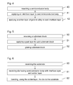
- FIGS. 4 to 6 show a flow charts illustrating an example method of forming the die, substrate and a package.
- FIG. 1 shows a semiconductor die 1 and a metal substrate 2 for die bonding together using solder.
- the substrate also known as a header or flange, may comprise a heat sink for the RF power package. It is important that fabrication costs are low while ensuring reliability of the resulting package.
- the relative thermal expansion between the semiconductor die 1 and substrate 2 needs to be managed, typically using expensive materials, while ensuring high thermal conductivity between the die 1 and the substrate 2 .
- the present embodiment provides a cost-effective die and substrate and fabrication process while maintaining a high integrity solder interconnect between the die and the substrate to ensure structural reliability and effective thermal transfer.
- the die 1 comprises a body 3 of semiconductor material, such as Silicon.
- the body 3 includes a solder layer 4 comprising an alloy containing gold for use in die bonding said die to the substrate 2 .
- the solder layer in some examples, may not contain gold.
- the die 1 includes an interface layer 5 between the body 3 and the solder layer 4 , the interface layer 5 having a plurality of sub-layers of different metals.
- the semiconductor body 3 is formed from a silicon wafer, which may have electronic components formed thereon.
- the body 3 may comprise a monocrystalline silicon or Gallium Arsenide or Gallium Nitride semiconducting material or any other semiconducting material.
- the backside of the body 3 has the interface layer 5 applied thereto.
- the interface layer comprises a plurality of sub-layers and may comprise a gold sub-layer adjacent the body 3 and a gold sub-layer adjacent the solder layer and at least one further sub-layer of a metal other than gold between the gold sub-layers.
- FIG. 2 shows the die 1 and the interface layer 5 in more detail.
- the interface layer 5 comprises, in this embodiment four sub-layers 5 a , 5 b , 5 c and 5 d .
- the first sub-layer 5 a is applied directly to the body 3 and comprises a layer of gold alloyed with the Si to obtain a low ohmic contact.
- the first sub-layer may be between 100 nm and 500 nm thick and preferably between 200 and 400 nm.
- the first sub-layer may have a lower limit thickness of 50 nm, 100 nm, 150 nm, 200 nm, 250 nm, 300 nm in combination with any of the following upper limit thicknesses 300 nm, 350 nm, 400 nm, 450 nm, 500 nm.
- the first sub-layer has a thickness of substantially 300 nm.
- the purity of the gold layer may be at least 80% or, preferably, at least 95% or at least 99% or substantially pure.
- the second sub-layer 5 b comprises, in this embodiment, a layer of silver applied to the first sub-layer 5 a .
- the second sub-layer 5 b may be thinner than the first sub-layer.
- the second sub-layer 5 b may be between 50 nm and 400 nm thick and preferably between 100 and 300 nm.
- the second sub-layer 5 b may have a lower limit thickness of 25 nm, 50 nm, 75 nm, 100 nm, 125 nm, 150 nm, 175 nm or 200 nm in combination with any of the following upper limit thicknesses 200 nm, 250 nm, 300 nm, 350 nm, 400 nm.
- the second sub-layer has a thickness of substantially 200 nm.
- the purity of the silver layer may be at least 80% or, preferably, at least 95% or at least 99% or substantially pure.
- the third sub-layer 5 c comprises, in this embodiment, a layer of nickel applied to the second sub-layer 5 c .
- the third sub-layer 5 c may be thicker than the second sub-layer and/or may be thinner than the first sub-layer 5 a .
- the third sub-layer 5 c may be between 100 nm and 450 nm thick and preferably between 200 and 350 nm.
- the third sub-layer 5 c may have a lower limit thickness of 75 nm, 100 nm, 125 nm, 150 nm, 175 nm, 200 nm, 225 nm or 250 nm in combination with any of the following upper limit thicknesses 250 nm, 300 nm, 350 nm, 400 nm, 450 nm.
- the third sub-layer has a thickness of substantially 250 nm.
- the purity of the nickel layer may be at least 80% or, preferably, at least 95% or at least 99% or substantially pure.
- the fourth sub-layer may be between 100 nm and 500 nm thick and preferably between 200 and 400 nm.
- the fourth sub-layer may have a lower limit thickness of 50 nm, 100 nm, 150 nm, 200 nm, 250 nm, 300 nm in combination with any of the following upper limit thicknesses 300 nm, 350 nm, 400 nm, 450 nm, 500 nm.
- the fourth sub-layer has a thickness of substantially 300 nm.
- the purity of the gold, fourth sub-layer may be at least 80% or, preferably, at least 95% or at least 99% or substantially pure.
- FIG. 3 shows the die 1 having the solder layer 4 applied to the interface layer and, in particular, the final (in this embodiment fourth) sub-layer of the interface layer 5 .
- the solder layer comprises a layer for use in a soldering process to bond the die 1 to the substrate 2 .
- the solder layer comprises, in this embodiment, an alloy of gold and tin (AuSn). The ratio of gold to tin in the alloy may be substantially 80/20 wt %.
- the solder layer may contain trace amounts of other substances. It has been found that the use of the interface layer may improve the integrity of the silicon die/solder bond.
- the solder layer may have a thickness of at least 2000 nm or at least 3000 nm or at least 4000 nm. However, it will be appreciated that the solder layer may have any thickness depending on the particular application. In this embodiment, the solder layer has a thickness of substantially between 5000 nm and 7000 nm depending on die size. Thus, the solder layer 4 may be at least three or four times the thickness of the interface layer 5 .
- the substrate 2 comprises a homogeneous block 6 of copper.
- the purity of the copper may be at least 80%, 90%, 95% or 99.8%.
- the substrate block 6 comprises at least/substantially 90% by mass of the substrate.
- the substrate is homogeneous in that it does not contain sub-layers of different metals or alloys. This is advantageous as it is cost-effective for the substrate to be of copper rather than other typical substrates such as CPC or CuW.
- the substrate may include a pad 7 .
- the pad 7 comprises a layer of silver disposed on at least part of a surface of the substrate 2 .
- the pad 7 may be sized to substantially correspond to the size of the die 1 that is secured to the substrate 2 .
- the silver pad 7 may have a purity of at least 90%, 95% or 98% or may be substantially pure.
- the substrate block 6 and possibly also the pad 7 may be plated with an outer layer 8 .
- the outer layer 8 comprises sub-layers of substantially pure nickel, palladium and gold (NiPdAu).
- NiPdAu substantially pure nickel, palladium and gold
- FIGS. 4, 5 and 6 comprise flow charts illustrating the various fabrication and assembly processes used to fabricate an RF power package according to an embodiment of the invention.
- FIG. 4 shows receiving the body 3 of semiconductor material at step 40 .
- Step 41 shows the application of the interface layer 5 to a backside of the body 3 .
- the sub-layers of the interface layer 5 may be applied by sputtering, evaporation or electroplating or any other thin-film deposition technique.
- step 41 includes applying the first, gold, sub-layer 5 a to the body 3 ; applying the second, silver, sub-layer 5 b to the first sub-layer 5 a; applying the third, nickel sub-layer 5 c to the second sub-layer 5 b ; and applying the fourth, gold, sub-layer 5 d to the third sub-layer 5 c .
- the body 3 with interface layer 5 may be supplied as such but the method may also include, as illustrated in step 42 , applying a gold-tin alloy solder layer 4 to the interface layer 5 .
- FIG. 5 shows the fabrication process for producing the substrate 2 ready for bonding to the die 1 .
- the process comprises receiving a copper substrate block 6 comprising the main body of the substrate 2 , at step 60 .
- Step 61 shows applying a pad layer 7 of gold over at least part of a die bond surface of the substrate for receiving the die 1 .
- the pad layer may be applied by any appropriate thin-film deposition technique.
- Step 62 shows electroplating the block 6 and pad layer with the outer layer 8 .
- FIG. 6 shows the steps of die bonding in which the die including the interface layer 5 and solder layer 4 is bonded to the substrate 2 including the pad layer 7 and outer plating layer 8 .
- Step 60 shows receiving the substrate 1 .
- Step 61 shows receiving the die comprising the semiconductor body 3 with interface layer 5 and solder layer 4 .
- Step 62 illustrates the die bonding step in which the solder layer is thermo-compression bonded or thermosonically bonded to solder the die 1 to the pad layer 7 of the substrate 2 .
- the interface layer may comprise a first sub-layer of gold and a second sub-layer of silver (AuAg).
- the interface layer may comprise a first sub-layer of gold, a second sub-layer of Nickel and a third sub-layer of Silver.
- Such an interface layer may be electroplated with a Nickel (Ni) layer.
Abstract
Description
-
- receiving a semiconductor body;
- applying an interface layer to said semiconductor body, said interface layer comprising a plurality of sub-layers of different metals.
Claims (9)
Applications Claiming Priority (3)
| Application Number | Priority Date | Filing Date | Title |
|---|---|---|---|
| EP13199587.0A EP2889903A1 (en) | 2013-12-24 | 2013-12-24 | Die with a multilayer backside interface layer for solder bonding to a substrate and corresponding manufacturing method |
| EP13199587 | 2013-12-24 | ||
| EP13199587.0 | 2013-12-24 |
Publications (2)
| Publication Number | Publication Date |
|---|---|
| US20150179599A1 US20150179599A1 (en) | 2015-06-25 |
| US9324674B2 true US9324674B2 (en) | 2016-04-26 |
Family
ID=49943142
Family Applications (1)
| Application Number | Title | Priority Date | Filing Date |
|---|---|---|---|
| US14/562,129 Active US9324674B2 (en) | 2013-12-24 | 2014-12-05 | Die substrate assembly and method |
Country Status (3)
| Country | Link |
|---|---|
| US (1) | US9324674B2 (en) |
| EP (1) | EP2889903A1 (en) |
| CN (1) | CN104733418A (en) |
Cited By (2)
| Publication number | Priority date | Publication date | Assignee | Title |
|---|---|---|---|---|
| US20150201515A1 (en) * | 2014-01-13 | 2015-07-16 | Rf Micro Devices, Inc. | Surface finish for conductive features on substrates |
| WO2020055244A1 (en) | 2018-09-10 | 2020-03-19 | Ampleon Netherlands B.V. | Seed layer for electroplating eutectic ausn solder |
Families Citing this family (3)
| Publication number | Priority date | Publication date | Assignee | Title |
|---|---|---|---|---|
| DE102016117389B4 (en) * | 2015-11-20 | 2020-05-28 | Semikron Elektronik Gmbh & Co. Kg | Power semiconductor chip and method for producing a power semiconductor chip and power semiconductor device |
| US9893027B2 (en) * | 2016-04-07 | 2018-02-13 | Nxp Usa, Inc. | Pre-plated substrate for die attachment |
| TWI638433B (en) * | 2017-10-24 | 2018-10-11 | 英屬維京群島商艾格生科技股份有限公司 | Element submount and manufacturing method thereof |
Citations (14)
| Publication number | Priority date | Publication date | Assignee | Title |
|---|---|---|---|---|
| JPS60110127A (en) | 1983-11-18 | 1985-06-15 | Sony Corp | Semiconductor device having laminated metal electrode |
| US5698897A (en) | 1995-01-27 | 1997-12-16 | Nec Corporation | Semiconductor device having a plated heat sink |
| US20060108672A1 (en) | 2004-11-24 | 2006-05-25 | Brennan John M | Die bonded device and method for transistor packages |
| US20070181986A1 (en) * | 2004-03-24 | 2007-08-09 | Tokuyama Corporation | Substrate for device bonding and method for manufacturing same |
| US20080054439A1 (en) * | 2006-08-29 | 2008-03-06 | Denso Corporation | Power electronic package having two substrates with multiple semiconductor chips and electronic components |
| WO2008050251A1 (en) | 2006-10-23 | 2008-05-02 | Nxp B.V. | Backside wafer contact structure and method of forming the same |
| US20080128908A1 (en) * | 2006-11-09 | 2008-06-05 | Quantum Leap Packaging, Inc. | Microcircuit package having ductile layer |
| US20090207580A1 (en) * | 2005-03-18 | 2009-08-20 | Yoshikazu Oshika | Submount and Method of Manufacturing the Same |
| US20110089465A1 (en) * | 2008-03-25 | 2011-04-21 | Lin Charles W C | Semiconductor chip assembly with post/base heat spreader with esd protection layer |
| US20120025387A1 (en) * | 2010-07-27 | 2012-02-02 | Kuo-Ching Chang | Chip package and fabricating method thereof |
| EP2453474A1 (en) | 2010-11-10 | 2012-05-16 | Nxp B.V. | Semiconductor device packaging method and semiconductor device package |
| JP2012178438A (en) | 2011-02-25 | 2012-09-13 | Omron Corp | Structure having metal layer for die bonding provided on n-type semiconductor substrate and method for manufacturing the same |
| US20130043594A1 (en) * | 2011-08-10 | 2013-02-21 | Kabushiki Kaisha Toshiba | Method for manufacturing semiconductor device and semiconductor device |
| EP2693465A1 (en) | 2012-07-31 | 2014-02-05 | Nxp B.V. | Electronic device and method of manufacturing such device |
-
2013
- 2013-12-24 EP EP13199587.0A patent/EP2889903A1/en not_active Withdrawn
-
2014
- 2014-12-05 US US14/562,129 patent/US9324674B2/en active Active
- 2014-12-22 CN CN201410806694.8A patent/CN104733418A/en active Pending
Patent Citations (14)
| Publication number | Priority date | Publication date | Assignee | Title |
|---|---|---|---|---|
| JPS60110127A (en) | 1983-11-18 | 1985-06-15 | Sony Corp | Semiconductor device having laminated metal electrode |
| US5698897A (en) | 1995-01-27 | 1997-12-16 | Nec Corporation | Semiconductor device having a plated heat sink |
| US20070181986A1 (en) * | 2004-03-24 | 2007-08-09 | Tokuyama Corporation | Substrate for device bonding and method for manufacturing same |
| US20060108672A1 (en) | 2004-11-24 | 2006-05-25 | Brennan John M | Die bonded device and method for transistor packages |
| US20090207580A1 (en) * | 2005-03-18 | 2009-08-20 | Yoshikazu Oshika | Submount and Method of Manufacturing the Same |
| US20080054439A1 (en) * | 2006-08-29 | 2008-03-06 | Denso Corporation | Power electronic package having two substrates with multiple semiconductor chips and electronic components |
| WO2008050251A1 (en) | 2006-10-23 | 2008-05-02 | Nxp B.V. | Backside wafer contact structure and method of forming the same |
| US20080128908A1 (en) * | 2006-11-09 | 2008-06-05 | Quantum Leap Packaging, Inc. | Microcircuit package having ductile layer |
| US20110089465A1 (en) * | 2008-03-25 | 2011-04-21 | Lin Charles W C | Semiconductor chip assembly with post/base heat spreader with esd protection layer |
| US20120025387A1 (en) * | 2010-07-27 | 2012-02-02 | Kuo-Ching Chang | Chip package and fabricating method thereof |
| EP2453474A1 (en) | 2010-11-10 | 2012-05-16 | Nxp B.V. | Semiconductor device packaging method and semiconductor device package |
| JP2012178438A (en) | 2011-02-25 | 2012-09-13 | Omron Corp | Structure having metal layer for die bonding provided on n-type semiconductor substrate and method for manufacturing the same |
| US20130043594A1 (en) * | 2011-08-10 | 2013-02-21 | Kabushiki Kaisha Toshiba | Method for manufacturing semiconductor device and semiconductor device |
| EP2693465A1 (en) | 2012-07-31 | 2014-02-05 | Nxp B.V. | Electronic device and method of manufacturing such device |
Non-Patent Citations (2)
| Title |
|---|
| Extended European Search Report for application 13199587.0 (Jun. 5, 2014). |
| Lui, Xingsheng et al; "Design and Implementation of Metallization on Structures for Epi-Down Bonded High Power Semiconductor Lasers"; Proceedings Electronic Components and Technology Conference, vol. 1, Las Vegas, NV, US; IEEE, Piscataway, NJ, US; pp. 798-806 (Jun. 2004). |
Cited By (3)
| Publication number | Priority date | Publication date | Assignee | Title |
|---|---|---|---|---|
| US20150201515A1 (en) * | 2014-01-13 | 2015-07-16 | Rf Micro Devices, Inc. | Surface finish for conductive features on substrates |
| WO2020055244A1 (en) | 2018-09-10 | 2020-03-19 | Ampleon Netherlands B.V. | Seed layer for electroplating eutectic ausn solder |
| NL2021598B1 (en) | 2018-09-10 | 2020-05-01 | Ampleon Netherlands Bv | Seed layer for electroplating eutectic AuSn solder |
Also Published As
| Publication number | Publication date |
|---|---|
| EP2889903A1 (en) | 2015-07-01 |
| CN104733418A (en) | 2015-06-24 |
| US20150179599A1 (en) | 2015-06-25 |
Similar Documents
| Publication | Publication Date | Title |
|---|---|---|
| TWI484608B (en) | Solder bump/under bump metallurgy structure for high temperature applications | |
| US9324674B2 (en) | Die substrate assembly and method | |
| EP1748480B1 (en) | Connection structure for attaching a semiconductor chip to a metal substrate, semiconductor chip and electronic component including the connection structure and methods for producing the connection structure | |
| CN101350381B (en) | Salient point LED and manufacturing method thereof | |
| US20240088087A1 (en) | Electronic device with multi-layer contact and system | |
| US8021929B2 (en) | Apparatus and method configured to lower thermal stresses | |
| USRE43807E1 (en) | Microcircuit package having ductile layer | |
| JPH08181392A (en) | Bonding material and bonding method of electric element | |
| US20080242003A1 (en) | Integrated circuit devices with integral heat sinks | |
| US8193070B2 (en) | Method for bonding layers, corresponding device and organic light-emitting diode | |
| US8283756B2 (en) | Electronic component with buffer layer | |
| KR20180095590A (en) | Method for manufacturing power semiconductor device and power semiconductor device | |
| US6376910B1 (en) | Solder-on back metal for semiconductor die | |
| EP2693465A1 (en) | Electronic device and method of manufacturing such device | |
| WO2008050251A1 (en) | Backside wafer contact structure and method of forming the same | |
| US9123704B2 (en) | Semiconductor device and method for manufacturing the same | |
| TWM582236U (en) | Power module package | |
| JPH08115928A (en) | Semiconductor device, and its manufacture | |
| US20090166852A1 (en) | Semiconductor packages with thermal interface materials | |
| US8188592B2 (en) | Apparatus and method configured to lower thermal stresses | |
| TW201308543A (en) | Bonded structure | |
| WO2020055244A1 (en) | Seed layer for electroplating eutectic ausn solder | |
| JPH03218031A (en) | Semiconductor integrated circuit device and preform bonding material used in the same | |
| CN113140537A (en) | Power semiconductor device and method for producing a power semiconductor device |
Legal Events
| Date | Code | Title | Description |
|---|---|---|---|
| AS | Assignment |
Owner name: NXP, B.V., NETHERLANDS Free format text: ASSIGNMENT OF ASSIGNORS INTEREST;ASSIGNORS:VAN RIJCKEVORSEL, JOHANNES WILHELMUS;DE BRUIN, EMIEL;REEL/FRAME:034395/0812 Effective date: 20140314 |
|
| AS | Assignment |
Owner name: SAMBA HOLDCO NETHERLANDS B.V., NETHERLANDS Free format text: ASSIGNMENT OF ASSIGNORS INTEREST;ASSIGNOR:NXP B.V.;REEL/FRAME:036630/0574 Effective date: 20150904 |
|
| FEPP | Fee payment procedure |
Free format text: PAYOR NUMBER ASSIGNED (ORIGINAL EVENT CODE: ASPN); ENTITY STATUS OF PATENT OWNER: LARGE ENTITY |
|
| AS | Assignment |
Owner name: AMPLEON NETHERLANDS B.V., NETHERLANDS Free format text: CHANGE OF NAME;ASSIGNOR:SAMBA HOLDCO NETHERLANDS B.V.;REEL/FRAME:037876/0873 Effective date: 20151207 |
|
| AS | Assignment |
Owner name: MORGAN STANLEY SENIOR FUNDING, INC., MARYLAND Free format text: SECURITY AGREEMENT SUPPLEMENT;ASSIGNOR:NXP B.V.;REEL/FRAME:038017/0058 Effective date: 20160218 |
|
| STCF | Information on status: patent grant |
Free format text: PATENTED CASE |
|
| AS | Assignment |
Owner name: MORGAN STANLEY SENIOR FUNDING, INC., MARYLAND Free format text: CORRECTIVE ASSIGNMENT TO CORRECT THE REMOVE APPLICATION 12092129 PREVIOUSLY RECORDED ON REEL 038017 FRAME 0058. ASSIGNOR(S) HEREBY CONFIRMS THE SECURITY AGREEMENT SUPPLEMENT;ASSIGNOR:NXP B.V.;REEL/FRAME:039361/0212 Effective date: 20160218 |
|
| AS | Assignment |
Owner name: NXP B.V., NETHERLANDS Free format text: PATENT RELEASE;ASSIGNOR:MORGAN STANLEY SENIOR FUNDING, INC.;REEL/FRAME:039707/0471 Effective date: 20160805 |
|
| AS | Assignment |
Owner name: MORGAN STANLEY SENIOR FUNDING, INC., MARYLAND Free format text: CORRECTIVE ASSIGNMENT TO CORRECT THE REMOVE APPLICATION 12681366 PREVIOUSLY RECORDED ON REEL 039361 FRAME 0212. ASSIGNOR(S) HEREBY CONFIRMS THE SECURITY AGREEMENT SUPPLEMENT;ASSIGNOR:NXP B.V.;REEL/FRAME:042762/0145 Effective date: 20160218 Owner name: MORGAN STANLEY SENIOR FUNDING, INC., MARYLAND Free format text: CORRECTIVE ASSIGNMENT TO CORRECT THE REMOVE APPLICATION 12681366 PREVIOUSLY RECORDED ON REEL 038017 FRAME 0058. ASSIGNOR(S) HEREBY CONFIRMS THE SECURITY AGREEMENT SUPPLEMENT;ASSIGNOR:NXP B.V.;REEL/FRAME:042985/0001 Effective date: 20160218 |
|
| AS | Assignment |
Owner name: NXP B.V., NETHERLANDS Free format text: RELEASE BY SECURED PARTY;ASSIGNOR:MORGAN STANLEY SENIOR FUNDING, INC.;REEL/FRAME:050745/0001 Effective date: 20190903 |
|
| AS | Assignment |
Owner name: MORGAN STANLEY SENIOR FUNDING, INC., MARYLAND Free format text: CORRECTIVE ASSIGNMENT TO CORRECT THE REMOVE APPLICATION 12298143 PREVIOUSLY RECORDED ON REEL 039361 FRAME 0212. ASSIGNOR(S) HEREBY CONFIRMS THE SECURITY AGREEMENT SUPPLEMENT;ASSIGNOR:NXP B.V.;REEL/FRAME:051029/0387 Effective date: 20160218 Owner name: MORGAN STANLEY SENIOR FUNDING, INC., MARYLAND Free format text: CORRECTIVE ASSIGNMENT TO CORRECT THE REMOVE APPLICATION 12298143 PREVIOUSLY RECORDED ON REEL 042985 FRAME 0001. ASSIGNOR(S) HEREBY CONFIRMS THE SECURITY AGREEMENT SUPPLEMENT;ASSIGNOR:NXP B.V.;REEL/FRAME:051029/0001 Effective date: 20160218 Owner name: MORGAN STANLEY SENIOR FUNDING, INC., MARYLAND Free format text: CORRECTIVE ASSIGNMENT TO CORRECT THE REMOVE APPLICATION 12298143 PREVIOUSLY RECORDED ON REEL 042762 FRAME 0145. ASSIGNOR(S) HEREBY CONFIRMS THE SECURITY AGREEMENT SUPPLEMENT;ASSIGNOR:NXP B.V.;REEL/FRAME:051145/0184 Effective date: 20160218 Owner name: MORGAN STANLEY SENIOR FUNDING, INC., MARYLAND Free format text: CORRECTIVE ASSIGNMENT TO CORRECT THE REMOVE APPLICATION12298143 PREVIOUSLY RECORDED ON REEL 039361 FRAME 0212. ASSIGNOR(S) HEREBY CONFIRMS THE SECURITY AGREEMENT SUPPLEMENT;ASSIGNOR:NXP B.V.;REEL/FRAME:051029/0387 Effective date: 20160218 Owner name: MORGAN STANLEY SENIOR FUNDING, INC., MARYLAND Free format text: CORRECTIVE ASSIGNMENT TO CORRECT THE REMOVE APPLICATION 12298143 PREVIOUSLY RECORDED ON REEL 038017 FRAME 0058. ASSIGNOR(S) HEREBY CONFIRMS THE SECURITY AGREEMENT SUPPLEMENT;ASSIGNOR:NXP B.V.;REEL/FRAME:051030/0001 Effective date: 20160218 Owner name: MORGAN STANLEY SENIOR FUNDING, INC., MARYLAND Free format text: CORRECTIVE ASSIGNMENT TO CORRECT THE REMOVE APPLICATION12298143 PREVIOUSLY RECORDED ON REEL 042985 FRAME 0001. ASSIGNOR(S) HEREBY CONFIRMS THE SECURITY AGREEMENT SUPPLEMENT;ASSIGNOR:NXP B.V.;REEL/FRAME:051029/0001 Effective date: 20160218 Owner name: MORGAN STANLEY SENIOR FUNDING, INC., MARYLAND Free format text: CORRECTIVE ASSIGNMENT TO CORRECT THE REMOVE APPLICATION12298143 PREVIOUSLY RECORDED ON REEL 042762 FRAME 0145. ASSIGNOR(S) HEREBY CONFIRMS THE SECURITY AGREEMENT SUPPLEMENT;ASSIGNOR:NXP B.V.;REEL/FRAME:051145/0184 Effective date: 20160218 |
|
| MAFP | Maintenance fee payment |
Free format text: PAYMENT OF MAINTENANCE FEE, 4TH YEAR, LARGE ENTITY (ORIGINAL EVENT CODE: M1551); ENTITY STATUS OF PATENT OWNER: LARGE ENTITY Year of fee payment: 4 |
|
| FEPP | Fee payment procedure |
Free format text: MAINTENANCE FEE REMINDER MAILED (ORIGINAL EVENT CODE: REM.); ENTITY STATUS OF PATENT OWNER: LARGE ENTITY |