US9240539B2 - Efficient polarization independent single photon detector - Google Patents

Efficient polarization independent single photon detector Download PDF

Info

Publication number
US9240539B2
US9240539B2 US13/869,802 US201313869802A US9240539B2 US 9240539 B2 US9240539 B2 US 9240539B2 US 201313869802 A US201313869802 A US 201313869802A US 9240539 B2 US9240539 B2 US 9240539B2
Authority
US
United States
Prior art keywords
layer
superconducting
meander pattern
nanometers
comprised
Prior art date
Legal status (The legal status is an assumption and is not a legal conclusion. Google has not performed a legal analysis and makes no representation as to the accuracy of the status listed.)
Active, expires
Application number
US13/869,802
Other versions
US20140087952A1 (en
Inventor
Sae Woo Nam
Burm Baek
Francesco Marsilli
Varun Verma
Current Assignee (The listed assignees may be inaccurate. Google has not performed a legal analysis and makes no representation or warranty as to the accuracy of the list.)
National Institute of Standards and Technology (NIST)
Original Assignee
National Institute of Standards and Technology (NIST)
Priority date (The priority date is an assumption and is not a legal conclusion. Google has not performed a legal analysis and makes no representation as to the accuracy of the date listed.)
Filing date
Publication date
Application filed by National Institute of Standards and Technology (NIST) filed Critical National Institute of Standards and Technology (NIST)
Priority to US13/869,802 priority Critical patent/US9240539B2/en
Publication of US20140087952A1 publication Critical patent/US20140087952A1/en
Assigned to GOVERNMENT OF THE UNITED STATES OF AMERICA, AS REPRESENTED BY THE SECRETARY OF COMMERCE, THE NATIONAL INSTITUTE OF STANDARDS AND TECHNOLOGY reassignment GOVERNMENT OF THE UNITED STATES OF AMERICA, AS REPRESENTED BY THE SECRETARY OF COMMERCE, THE NATIONAL INSTITUTE OF STANDARDS AND TECHNOLOGY ASSIGNMENT OF ASSIGNORS INTEREST (SEE DOCUMENT FOR DETAILS). Assignors: NAM, SAE WOO
Assigned to GOVERNMENT OF THE UNITED STATES OF AMERICA, AS REPRESENTED BY THE SECRETARY OF COMMERCE, THE NATIONAL INSTITUTE OF STANDARDS AND TECHNOLOGY reassignment GOVERNMENT OF THE UNITED STATES OF AMERICA, AS REPRESENTED BY THE SECRETARY OF COMMERCE, THE NATIONAL INSTITUTE OF STANDARDS AND TECHNOLOGY ASSIGNMENT OF ASSIGNORS INTEREST (SEE DOCUMENT FOR DETAILS). Assignors: MARSILI, Francesco, VERMA, VARUN BOEHM, NAM, SAE WOO
Priority to US14/698,442 priority patent/US9577175B1/en
Application granted granted Critical
Publication of US9240539B2 publication Critical patent/US9240539B2/en
Active legal-status Critical Current
Adjusted expiration legal-status Critical

Links

Images

Classifications

    • HELECTRICITY
    • H10SEMICONDUCTOR DEVICES; ELECTRIC SOLID-STATE DEVICES NOT OTHERWISE PROVIDED FOR
    • H10NELECTRIC SOLID-STATE DEVICES NOT OTHERWISE PROVIDED FOR
    • H10N60/00Superconducting devices
    • H10N60/80Constructional details
    • GPHYSICS
    • G01MEASURING; TESTING
    • G01JMEASUREMENT OF INTENSITY, VELOCITY, SPECTRAL CONTENT, POLARISATION, PHASE OR PULSE CHARACTERISTICS OF INFRARED, VISIBLE OR ULTRAVIOLET LIGHT; COLORIMETRY; RADIATION PYROMETRY
    • G01J1/00Photometry, e.g. photographic exposure meter
    • G01J1/02Details
    • G01J1/04Optical or mechanical part supplementary adjustable parts
    • G01J1/0407Optical elements not provided otherwise, e.g. manifolds, windows, holograms, gratings
    • G01J1/0425Optical elements not provided otherwise, e.g. manifolds, windows, holograms, gratings using optical fibers
    • H01L39/02
    • GPHYSICS
    • G01MEASURING; TESTING
    • G01JMEASUREMENT OF INTENSITY, VELOCITY, SPECTRAL CONTENT, POLARISATION, PHASE OR PULSE CHARACTERISTICS OF INFRARED, VISIBLE OR ULTRAVIOLET LIGHT; COLORIMETRY; RADIATION PYROMETRY
    • G01J1/00Photometry, e.g. photographic exposure meter
    • G01J1/42Photometry, e.g. photographic exposure meter using electric radiation detectors
    • H01L39/10
    • H01L39/12
    • H01L39/24
    • HELECTRICITY
    • H10SEMICONDUCTOR DEVICES; ELECTRIC SOLID-STATE DEVICES NOT OTHERWISE PROVIDED FOR
    • H10NELECTRIC SOLID-STATE DEVICES NOT OTHERWISE PROVIDED FOR
    • H10N60/00Superconducting devices
    • H10N60/01Manufacture or treatment
    • HELECTRICITY
    • H10SEMICONDUCTOR DEVICES; ELECTRIC SOLID-STATE DEVICES NOT OTHERWISE PROVIDED FOR
    • H10NELECTRIC SOLID-STATE DEVICES NOT OTHERWISE PROVIDED FOR
    • H10N60/00Superconducting devices
    • H10N60/80Constructional details
    • H10N60/84Switching means for devices switchable between superconducting and normal states
    • HELECTRICITY
    • H10SEMICONDUCTOR DEVICES; ELECTRIC SOLID-STATE DEVICES NOT OTHERWISE PROVIDED FOR
    • H10NELECTRIC SOLID-STATE DEVICES NOT OTHERWISE PROVIDED FOR
    • H10N60/00Superconducting devices
    • H10N60/80Constructional details
    • H10N60/85Superconducting active materials
    • GPHYSICS
    • G01MEASURING; TESTING
    • G01JMEASUREMENT OF INTENSITY, VELOCITY, SPECTRAL CONTENT, POLARISATION, PHASE OR PULSE CHARACTERISTICS OF INFRARED, VISIBLE OR ULTRAVIOLET LIGHT; COLORIMETRY; RADIATION PYROMETRY
    • G01J1/00Photometry, e.g. photographic exposure meter
    • G01J1/42Photometry, e.g. photographic exposure meter using electric radiation detectors
    • G01J1/44Electric circuits
    • G01J2001/4413Type
    • G01J2001/442Single-photon detection or photon counting

Definitions

  • the present invention relates to the field of single photon detectors, and more specifically to a photon detector which more efficiently detects photons in low light environments.
  • FIG. 1 is a cut-away perspective of an exemplary single layer superconductive nanowire meander pattern using a tungsten silicide (TS) nanowire.
  • TS tungsten silicide
  • FIG. 2 is a top view of an exemplary single layer superconductive nanowire illustrating a meander pattern using a tungsten silicide (TS) nanowire.
  • TS tungsten silicide
  • FIG. 3 is a side sectional perspective view of an exemplary embodiment of a multilayer polarization independent superconducting nanowire avalanche photo-detector (SNAP) microelectronic circuit.
  • SNAP nanowire avalanche photo-detector
  • FIG. 4 a is a scanning electron micrograph of an exemplary embodiment of a multilayer SNAP microelectronic circuit.
  • FIG. 4 b is a close-up scanning electron micrograph of an exemplary embodiment of a multilayer SNAP microelectronic circuit.
  • FIG. 5 is a wiring diagram of how an exemplary embodiment of a multilayer SNAP microelectronic circuit is wired.
  • FIG. 6 a is a top perspective view of an exemplary embodiment of a multilayer SNAP device.
  • FIG. 6 b is a diagram of the optical components of an exemplary embodiment of a multilayer SNAP test system.
  • FIG. 7 a is a plot showing the system detection efficiency (SDE) of an exemplary embodiment of a multilayer SNAP device as a function of bias current.
  • SDE system detection efficiency
  • FIG. 7 b is a plot showing the dark count rate (OCR) of an exemplary embodiment of a multilayer SNAP device as a function of bias current.
  • FIG. 8 a is a map of the single-photon detection efficiency (SDE) over the Poincaré sphere of an exemplary embodiment of a multilayer SNAP device.
  • FIG. 8 b is a map of the single-photon detection efficiency (SDE) over the Poincaré sphere of a standard superconducting nanowire single photon detector (SN-SPD) device.
  • SDE single-photon detection efficiency
  • FIG. 9 a is a plot of the maximum and minimum SDE over the Poincaré sphere of an exemplary embodiment of a multilayer SNAP device.
  • FIG. 9 b is a plot of the ratio of the maximum to minimum SDE (SDE max /SDE min ) as a function of wavelength for a InGaAs power meter and for an exemplary embodiment of a multilayer SNAP device.
  • nonmetallic material refers to a material which is not metallic.
  • non-metallic materials includes materials such as silicon known as metalloids.
  • continuous meander pattern refers to a microelectronic circuit characterized by a series parallel circuit lines joined by curved segments to form a continuous electrically continuous twisting and turning pattern made by a nanowire.
  • patterned refers to the attachment and definition of a layer of material in the form of a specified pattern on a base material.
  • electrically connected refers to components connected in such a way that electrons can flow between them.
  • orthogonally refers to the relationship of two intersecting lines in a common plane or the relationship of two lines in different planes which would intersect each other if superimposed in a common plane.
  • orthogonally refers to the relationship of two meander patterns having segments which are perpendicular or substantially perpendicular to each other.
  • reactive surface superconductive nanowire single photon detector microelectronic circuit means the combined surface of the continuous meander pattern of superconductive nanowires available to photons on the surface of the microelectronic circuit.
  • SNAP means a superconducting nanowire avalanche photo-detector.
  • tungsten-silicon alloy or “tungsten silicide (TS)” means an amorphous material.
  • detection area refers to the area on a photo detection microcircuit device which is capable of detecting photons.
  • Photons are characterized by their wavelength, their polarization, and by their location in time and space.
  • a single photon detector is a device which produces an electrical signal when a single photon is absorbed by the detector.
  • SPD's include a single photon detector component which absorbs the photon and undergoes a change in state which produces the electrical signal.
  • Recently single photon detector components have taken the form of solid state microelectronic circuits made using fabrication methods known in the art of solid state microelectronics. SPD devices also include optical components necessary to direct the light to the SPD microelectronic circuit and electrical components to amplify and process the electrical signals produced by the microelectronic circuit.
  • SPD's are widely used in scientific research in the fields of medicine, biology, astronomy, physics, chemistry, electrical and chemical engineering, material science, and aeronautics. Additionally, single-photon detectors are an essential tool for a wide range of applications in quantum information, quantum communications, and quantum optics.
  • the effectiveness of a photon detection device is measured in terms efficiency. Ideally the detector should produce a signal every time a single photon enters the device. The probability that an electrical signal will be produced when a photon enters the SPD (expressed as a percent) is referred to as the system efficiency. The probability that a photon contacting the SPD microelectronic circuit will produce an electrical signal is known as the quantum efficiency of the microelectronic circuit.
  • the wavelength, polarization, and the position of the light all affect the system efficiency of the SPD device, and quantum efficiency of the microelectronic circuit. The system efficiency can be no greater, and is frequently less, than the quantum efficiency of the microelectronic circuit.
  • SPD's used to determine their suitability for certain applications are: signal-to-noise ratio, timing jitter, reset times, and dark count rate.
  • Signal to noise ratio is the ratio of magnitude of the electrical signal produced from the device to the magnitude of electrical noise of the device.
  • Timing jitter is the deviation of the measured photon arrival time from the actual photon arrival time.
  • Reset time is the time it takes for the device to be reset to receive another photon after an initial photon is detected.
  • Dark count rate is the number of (false) detection signals produced per unit time when no photons are entering the device. For SPD's to be useful in the widest possible applications they should have high signal-to-noise, low timing jitter, fast reset times, and low dark count rates.
  • APD avalanche photodiode
  • SN-SPDs based on niobium nitride (NbN) superconducting nanowires have demonstrated desirable properties 30 picoseconds timing jitter, fast reset times on the order of 10 nanoseconds, and low dark count rates below 1 kcps (thousand counts per second), but generally suffer from low system detection efficiencies of less than 20%.
  • the efficiency of these detectors depends strongly on the polarization of the incident light.
  • NbN nanowires known in the art are arranged in a continuous meander pattern across the surface of the detector microelectronic circuit. In theory, larger geometric area covered by the nanowires should translate into a proportionately larger quantum efficiency of the microelectronic circuit.
  • nanowires frequently have width dimensions of the order of the channels separating the nanowires from each other.
  • Nanowires may have an approximate thickness of 5 nm and an approximate width of 100 nm.
  • Current electron beam fabrication methods make it extremely difficult to create nanowires and channel features smaller than 100 nanometers.
  • a limiting factor governing the quantum efficiency of SN-SPD microelectronic circuits based on NbN is that they have a relatively small area where absorption of photons may take place.
  • SPD devices experience decreased quantum efficiencies for photons having longer wave lengths.
  • SNSPD's Another problem known in the art is that the detection efficiency of SNSPD's depends upon the polarization of the light. There is an unmet need for superconducting SPDs which can detect photons with close to 100% efficiency for any photon wavelength, and any photon polarization. It is desirable to have SN-SPD technologies which provide larger areas for the absorption of photons within a designated physical area of the microelectronic circuit. It is desirable to have SN-SPD's with high signal-to-noise.
  • the invention is a polarization independent superconducting nanowire avalanche photo-detector apparatus which has higher quantum efficiency and signal-to-noise than any superconducting nanowire single photon detectors known in the art.
  • the present invention includes a three dimensional single superconducting nanowire single photon detector (SN-SPD) microelectronic circuit which has higher quantum efficiency than of SN-SPD's known in the art. This is achieved because the unique material and configuration of the microelectronic circuit eliminates the polarization dependence and shows improved signal-to-noise over SN-SPD microelectronic circuits known in the art. This objective is achieved by vertically stacking two tungsten-silicide (TS)-SN-SPDs made of amorphous tungsten silicide (TS) and electrically connecting them in parallel. This structure forms a multilayer superconducting nanowire avalanche photo-detector (SNAP).
  • SNAP multilayer superconducting nanowire avalanche photo-detector
  • a single photon detection device employing the multilayer (SNAP) microcircuit demonstrates a peak system detection efficiency of 87.7% and a polarization dependence of less than 2%. This represents nearly an order of magnitude improvement in both system detection efficiency and reduction of polarization dependence compared to conventional SNSPDs.
  • FIG. 1 is a cut-away perspective of an exemplary single layer superconductive nanowire continuous meander pattern 100 using a tungsten silicide (TS) nanowire.
  • FIG. 1 illustrates the prior art of a tungsten silicide (TS) nanowire sections 20 a through 20 n .
  • the complete geometric pattern of the nanowire is referred to as a continuous meander pattern (shown in FIG. 2 ).
  • Nanowire sections 20 a through 20 n are formed on an oxidized silicon substrate, which is a wafer of silicon on which a silicon oxide layer 12 has been created using a process known in the art.
  • the illustrated embodiment was prepared by co-sputtering tungsten and silicon to a thickness of 4.5 nanometers. Then a poly(methylmethacrylate) resist was applied, and imaged using an electron beam. The areas revealed by the exposed resist are etched by reactive ion etching in sulfur hexafluoride.
  • the area etched by reactive ion etching in the embodiment shown forms the etched channel spaces 25 a through n , and the areas protected by the resist form the nanowire shown as nanowire sections 20 a through 20 n .
  • the nanowires have a superconducting critical temperature of 3K, and an amorphous structure.
  • the tungsten silicide (TS) nanowire sections 20 a through 20 n are 150 nm wide and 4.5 nm thick.
  • FIG. 1 illustrates etched channel spaces 25 a through 25 n which in the present embodiment is 100 nanometers wide.
  • tungsten silicide (TS) nanowire sections 20 a through 20 n are comprised of 25 mole percent silicon, and 75 mole percent tungsten (W 0.75 Si 0.25 ).
  • TS tungsten silicide
  • the use of a tungsten silicide nanowire overcomes the manufacturing yield limitations of devices based on the conventional niobium nitride (NbN) superconductors because the amorphous tungsten silicide is less sensitive to defects than is the polycrystalline niobium nitride.
  • FIG. 2 is a top perspective view of a superconductive nanowire detector microelectronic circuit 100 in the prior art illustrating the nanowire continuous meander pattern 30 and bonding pads 11 a , and 11 b .
  • the nanowire continuous meander pattern 30 has an area of 16 ⁇ m ⁇ 16 ⁇ m.
  • Nanowire 20 and bonding pads 11 a , and 11 b are fabricated without significant constriction in the wires that would suppress the superconductive critical current (I c ).
  • the silicon substrate 10 also can be seen at the base of the etched channel spaces 25 .
  • the etched channel spaces 25 are 100 nm wide, and lie between the TS nanowires 20 a through 20 n .
  • the coverage area of the TS nanowires 20 a through 20 n in the embodiment shown represents 60% of the area of the continuous meander pattern 30 .
  • FIG. 2 illustrates a nanowire continuous meander pattern 30 which in this embodiment covers an area of 16 ⁇ m ⁇ 16 ⁇ m.
  • SN-SPD's based on an amorphous superconductor, tungsten silicide (TS), show that the use of this material enables the fabrication of detectors with significantly wider nanowire geometries ( ⁇ 150 nm) and higher detection efficiencies (>90%) than NbN-based SNSPDs.
  • FIG. 2 also illustrates bonding pads 11 a , and 11 b allowing the microscopic continuous meander pattern to electrically interface with electronic testing equipment known in the art.
  • Tungsten silicide nanowires of the exemplary embodiment are superconductive at temperatures from 0 to 5K, dependent on the exact composition of the tungsten silicide alloy. At this temperature the nanowire has no resistance to the flow of current. The absorption of a photon under these conditions is believed to create a “hot spot” in the TS nanowire 20 .
  • FIG. 3 is a side sectional perspective view of an exemplary embodiment of a multilayer superconducting nanowire avalanche photo-detector (SNAP) microelectronic circuit 400 .
  • the exemplary embodiment showed in FIG. 3 illustrates a device architecture in which multiple nanowire continuous meander pattern sections are vertically stacked on top of each other. This architecture is referred as a multilayer SNAP.
  • FIG. 3 illustrates a top continuous meander pattern 44 a and a bottom continuous meander pattern 44 b separated by a dielectric layer 42 , and a silicon substrate 10 .
  • FIG. 3 also illustrates left bonding pad 30 a , and right bonding pad 30 b .
  • the arrangement allows the top continuous meander pattern 44 a , and the bottom continuous meander pattern to be electrically connected in parallel.
  • the multilayer superconducting nanowire avalanche photo-detector (SNAP) illustrated in FIG. 3 is a continuous nanowire meander pattern with N parallel sections, the bias current (I B ) must be increased beyond the avalanche threshold current I AV to ensure correct operation.
  • I B the bias current
  • I AV avalanche threshold current
  • N an electrical current N times higher than the current of a single section is diverted to the load resistor, and the signal-to-noise ratio is improved by a factor of N.
  • Nanowire detectors utilizing this parallel architecture with N sections have become known as cascade-switching super-conducting single-photon detectors or superconducting nanowire avalanche photo-detectors (N-SNAPs).
  • FIG. 3 shows vertically stacked the sections of SNAP's on top of each other.
  • This architecture is referred to as a multilayer (SNAP).
  • the two sections could be patterned independently, the two sets of nanowires shown in FIG. 3 are oriented at orthogonal angles with respect to one another.
  • the vertical stacking of orthogonal nanowire continuous meander patterns connected electrically in parallel has produced (1) a factor of ⁇ 2 higher signal-to-noise ratio than previously reported with TS SNSPDs; (2) polarization independent system detection efficiency (SDE) over a ⁇ 100 nm-wide wavelength range; and (3) system detection efficiencies greater than 85%, comparable to the best results achieved to date with planar SNSPDs.
  • SDE polarization independent system detection efficiency
  • Each section of the multilayer SNAP consists of a 16 micrometer ⁇ 16 micrometer nanowire continuous meander pattern with a nanowire width of 150 nm and a pitch of 350 nm.
  • the thickness of each TS layer is 4.5 nm, yielding a superconducting critical temperature (T c ) of approximately 3 K, slightly lower than the bulk T c of 5 K for tungsten silicide alloy with an optimized Si composition of approximately 25%.
  • T c superconducting critical temperature
  • These two nanowire meanders are separated by a 30 micrometer ⁇ 30 micrometer, 75 nanometer thick square pad of hydrogen silsesquioxane (HSQ), a negative-tone pattern-able electron beam resist that becomes amorphous silicon oxide after exposure to an electron beam.
  • HSQ hydrogen silsesquioxane
  • the amorphous silicon oxide layer serves as a dielectric (electrical insulator) between the two SNSPDs.
  • the top continuous meander pattern 44 a and the bottom continuous meander pattern 44 b are in contact with each other where the HSQ has been developed away on each side of the patterned silicon oxide square pad, so that the two sections are electrically connected in parallel.
  • a crystalline superconductor such as NbN directly on top of an amorphous material would be impossible without degradation of its superconducting properties
  • the amorphous nature of amorphous TS allows it to be deposited on silicon oxide without any degradation of the T c or the superconducting switching current (I SW ) of the top layer compared to the bottom layer.
  • the quality of both layers was tested by characterizing the superconducting properties of single detectors both on top of and underneath the silicon dioxide dielectric layer.
  • the multilayer SNAP was embedded in a stack of dielectric materials to optimize absorption at a wavelength of 1550 nm.
  • the stack is designed such that the antinode of the electric field was positioned halfway between the two TS detector layers, so that each detector layer absorbs an equal number of photons.
  • the stack consists of an aluminum mirror and ⁇ /4 layer of SiO 2 below the detector and four alternating layers of SiO 2 and silicon nitride above the detector.
  • a keyhole-shape was etched around the detector through the silicon substrate, and the resulting microelectronic circuit was removed, packaged, and aligned to a standard telecommunications single-mode optical fiber by use of a self-aligned packaging scheme.20
  • This simplified packaging scheme ensures excellent alignment (63 lm) between the detector and the optical fiber.
  • FIG. 4 a is a scanning electron micrograph of an exemplary embodiment of a multilayer SNAP microelectronic circuit 400 .
  • FIG. 4 shows the top continuous meander pattern 44 a as vertical lines and the bottom continuous meander pattern 44 b as lighter horizontal lines. The bottom continuous meander pattern is lighter because it is partially obscured by dielectric layer 42 .
  • FIG. 4 a also shows left bonding pad 30 a , and right bonding pad 30 b.
  • FIG. 4 b is a higher magnification scanning electron micrograph of an exemplary embodiment of a multilayer SNAP microelectronic circuit 400 .
  • FIG. 4 shows the top continuous meander pattern 44 a as vertical lines and the bottom meander pattern 44 b as lighter horizontal lines.
  • the bottom continuous meander pattern is lighter because it is partially obscured by dielectric layer 42 .
  • FIG. 5 is a wiring diagram of how an exemplary embodiment of a multilayer SNAP microelectronic circuit is wired.
  • FIG. 5 illustrates a power supply 450 , a bias current 455 , a resistor 460 , top continuous meander pattern inductor element 470 , bottom continuous meander pattern inductor element 480 , and large inductor 490 .
  • Large inductor 490 is electrically connected in series with top continuous meander pattern inductor element 470 , and bottom continuous meander pattern inductor element 480 .
  • the large inductor 490 is fabricated on-microelectronic circuit in the top layer of tungsten silicide away from the detector area and is not illustrated in FIG. 3 .
  • FIG. 6 a is a top perspective view of an exemplary embodiment of a multilayer SNAP device 200 .
  • FIG. 6 a shows optical fiber 50 , coaxial connectors 90 , and thermal housing 120 .
  • the detector is mounted inside an adiabatic demagnetization refrigerator and cooled to ⁇ 150 milliK for measurements of the SDE (defined as the probability of detecting a photon that has been coupled into the fiber) and dark count rate (DCR).
  • FIG. 6 b is a diagram of the optical components of an exemplary embodiment of a multilayer SNAP test system.
  • FIG. 6 b shows an exemplary embodiment of a multilayer SNAP test device 200 .
  • FIG. 6 b shows tunable laser 500 which in the exemplary embodiment illustrated is a 1 mW laser tunable from (1520 nm to 1630 nm) through a computer controlled polarization controller.
  • FIG. 6 b illustrates optical attenuators 520 , set to provide a count rate of approximately 50,000 photons/sec.
  • FIG. 6 b shows micro electro-mechanical system (MEMS) optical switch 530 used to switch between a power meter and the device under test. Before each measurement, the MEMS switch output was sent to the power meter for calibration of the number of photons per second incident on the detector, then switched to the device under test for measurement of the SDE.
  • MEMS micro electro-mechanical system
  • FIG. 7 a is a plot showing the system detection efficiency (SDE) of an exemplary embodiment of a multilayer SNAP device as a function of bias current.
  • SDE system detection efficiency
  • FIG. 7 b is a plot showing the dark count rate (DCR) of an exemplary embodiment of a multilayer SNAP device. Conditions used for the measurements shown in FIG. 7 b are the same as those for the measurements shown in FIG. 7 a .
  • the DCR is lower than 400 cps with a fiber coupled to the detector, which we attribute to stray blackbody radiation coupled into the fiber. Without a fiber coupled to the detector, the device exhibits a DCR of less than 0.1 cps.
  • the switching current of 9.8 microamperes is approximately twice the switching current of a typical single-layer SN-SPD. From the bias dependence of the SDE, we find an avalanche current I AV ⁇ 0.6 ⁇ I SW . The device exhibits a broad plateau in SDE over 40% of the bias range between the avalanche current and the switching current.
  • FIG. 8 a is a map of the single-photon detection efficiency (SDE) over the Poincaré sphere of an exemplary embodiment of a multilayer SNAP device.
  • the SDE values at 1560 nm are shown in a color scale and indicate the variation in efficiency over the whole range of possible polarizations.
  • AR axial ratio
  • tilt angle
  • the quantities 2 ⁇ and 2 ⁇ represent latitude and longitude on the Poincaré sphere.
  • the entire Poincaré sphere is mapped by ⁇ 90° ⁇ 2 ⁇ 90° and 0 ⁇ 2 ⁇ 360°.
  • FIG. 8 b is a map of the single-photon detection efficiency (SDE) over the Poincaré sphere of a standard superconducting nanowire single photon detector (SN-SPD) device.
  • the standard single-layer SNSPD exemplifying the prior art is a single-layer SNSPD had a wire width of 120 nanometers and a pitch of 220 nanometers.
  • the device was embedded in an optical stack consisting of (bottom to top) a gold mirror, a layer of sputtered SiO 2 , the tungsten silicide detector, a second layer of SiO 2 , and a sputtered layer of TiO 2 , with layer thicknesses optimized for absorption at 1550 nm. Note the difference in scales.
  • FIG. 8 a of multilayer SNAP device Comparing FIG. 8 a of multilayer SNAP device and FIG. 8 a of the SN-SPD device the multilayer SNAP device shows a variation of less than 2%, over the Poincaré sphere compared to the single-layer device, which shows a variation of approximately 16%.
  • FIG. 9 a is a plot of the maximum and minimum SDE over the Poincaré sphere of an exemplary embodiment of a multilayer SNAP device.
  • the SDE reaches a peak of 87.7% ⁇ 0.5% at 1540 nm, close to the design wavelength of 1550 nm. At shorter and longer wavelengths, the SDE decreases due to the effects of the optical stack.
  • FIG. 9 b is a plot of the ratio of the maximum to minimum SDE (SDE max /SDE min ) as a function of wavelength for an Indium-Gallium-Arsenide (InGaAs) power meter and for an exemplary embodiment of a multilayer SNAP device.
  • the ratio R DSE (SDE max /SDE min ) for the multilayer SNAP device (indicated by solid boxes) shows a minimum of 1.019 at 1560 nm and remains below 1.04 over the entire wavelength span from 1510 nm to 1630 nm.
  • the fact that R sDE never reaches unity is attributed to the polarization dependence of the optical components of the measurement setup. To support this contention FIG.
  • 9 b also shows the wavelength dependence of the ratio between the maximum and minimum power measured by an InGaAs power meter while scanning the polarization over the Poincaré sphere, indicated by the blue triangles in FIG. 9 b .
  • the similarity in the polarization dependence of the components of the measurement setup is indicated by the overlap of the triangles overlap with the squares within the error bars of the measurement over a wavelength range from 1520 nm to 1580 nm, indicating that the primary source of the small polarization dependence is the measurement setup and suggesting that the multilayer SNAP itself is polarization independent.
  • the rise time, decay time, and dead time of the detector are important metrics.
  • a bias current of 9 microamperes an amplified voltage pulse height of 600 millivolts is measured with a rise time of 8 nanoseconds, a 1/e decay time of 57 nanoseconds, and a dead time (during which the system detection efficiency is suppressed) of 38 nanoseconds as estimated from inter-arrival time measurements.
  • the long rise and decay times are due to the large series inductor ( 490 in FIG. 5 ) being ten times the inductance of continuous meander pattern inductors ( 470 and 480 in FIG. 5 ), required to ensure stable operation of the SNAP.
  • the measured jitter is large relative to that of typical SNSPDs, it is significantly smaller than that of other single photon detectors such as transition edge sensors (TESs), and comparable to the jitter of commercially available Si APDs.
  • the jitter of 465 picoseconds is compatible with the measurement of multi-photon entangled states produced at a repetition rate of 80 MHz by a Ti:Sapphire mode-locked laser.
  • the mulitlayerSNAP would also provide for a smaller coincidence window than a TES in a loophole-free test of the Bell inequality allowing a smaller distance between detectors and improvement in the system detection efficiency in such a measurement.
  • the jitter of the mulitlayerSNAP may be reduced by reducing the value of the large inductor 490 in FIG.
  • the extension of the SNAP nanowire architecture into three-dimensions represents a significant advancement in single-photon detector technology. Improvements in optical stack design and fabrication and the use of a higher-fill-factor nanowire continuous meander pattern should allow for an SDE approaching 100%.
  • the significant reduction of the polarization dependence of the SDE will enhance the overall detection efficiency in experiments where the light is un-polarized and will eliminate the need for polarization controllers and wave-plates in experiments where the light is strongly polarized.
  • stacking more than two layers may provide a route to obtaining detection efficiencies approaching 100% that are less wavelength dependent, which may be important for applications requiring high detection efficiency over a broad range of wavelengths.

Abstract

A superconducting nanowire single photon detector (SN-SPD) microelectronic circuit is described which has higher quantum efficiency and signal-to-noise than any SN-SPD's known in the art. The material and configuration of the microelectronic circuit eliminates the polarization dependence and shows improved signal-to-noise over SN-SPD microelectronic circuits known in the art. The higher efficiency, polarization independence, and high signal-to-noise is achieved by vertically stacking two tungsten-silicide (TS) SN-SPDs and electrically connecting them in parallel. This structure forms a multilayer superconducting nanowire avalanche photo-detector (SNAP). A single photon detection device employing the multilayer (SNAP) microelectronic circuit demonstrates a peak system detection efficiency of 87.7% and a polarization dependence of less than 2%. This represents nearly an order of magnitude improvement in both system detection efficiency and reduction of polarization dependence compared to conventional SNSPDs.

Description

CROSS-REFERENCE TO RELATED APPLICATIONS
This application claims priority to U.S. Provisional Application No. 61/638,675 filed on Apr. 26, 2012.
STATEMENT OF GOVERNMENT INTEREST
The invention described herein was made by employees of the United States Government and may be manufactured and used by or for the Government of the United States of America for governmental purposes without the payment of any royalties thereon or therefor.
FIELD OF THE INVENTION
The present invention relates to the field of single photon detectors, and more specifically to a photon detector which more efficiently detects photons in low light environments.
BRIEF DESCRIPTION OF THE DRAWINGS
The patent or application file contains at least one drawing executed in color. Copies of this patent or patent application publication with color drawing(s) will be provided by the Office upon request and payment of the necessary fee.
FIG. 1 is a cut-away perspective of an exemplary single layer superconductive nanowire meander pattern using a tungsten silicide (TS) nanowire.
FIG. 2 is a top view of an exemplary single layer superconductive nanowire illustrating a meander pattern using a tungsten silicide (TS) nanowire.
FIG. 3 is a side sectional perspective view of an exemplary embodiment of a multilayer polarization independent superconducting nanowire avalanche photo-detector (SNAP) microelectronic circuit.
FIG. 4 a is a scanning electron micrograph of an exemplary embodiment of a multilayer SNAP microelectronic circuit.
FIG. 4 b is a close-up scanning electron micrograph of an exemplary embodiment of a multilayer SNAP microelectronic circuit.
FIG. 5 is a wiring diagram of how an exemplary embodiment of a multilayer SNAP microelectronic circuit is wired.
FIG. 6 a is a top perspective view of an exemplary embodiment of a multilayer SNAP device.
FIG. 6 b is a diagram of the optical components of an exemplary embodiment of a multilayer SNAP test system.
FIG. 7 a is a plot showing the system detection efficiency (SDE) of an exemplary embodiment of a multilayer SNAP device as a function of bias current.
FIG. 7 b is a plot showing the dark count rate (OCR) of an exemplary embodiment of a multilayer SNAP device as a function of bias current.
FIG. 8 a is a map of the single-photon detection efficiency (SDE) over the Poincaré sphere of an exemplary embodiment of a multilayer SNAP device.
FIG. 8 b is a map of the single-photon detection efficiency (SDE) over the Poincaré sphere of a standard superconducting nanowire single photon detector (SN-SPD) device.
FIG. 9 a is a plot of the maximum and minimum SDE over the Poincaré sphere of an exemplary embodiment of a multilayer SNAP device.
FIG. 9 b is a plot of the ratio of the maximum to minimum SDE (SDEmax/SDEmin) as a function of wavelength for a InGaAs power meter and for an exemplary embodiment of a multilayer SNAP device.
TERMS OF ART
As used herein the term “nonmetallic material” refers to a material which is not metallic. The term “non-metallic materials” includes materials such as silicon known as metalloids.
As used herein the term “continuous meander pattern” refers to a microelectronic circuit characterized by a series parallel circuit lines joined by curved segments to form a continuous electrically continuous twisting and turning pattern made by a nanowire.
As used herein the term “patterned” refers to the attachment and definition of a layer of material in the form of a specified pattern on a base material.
As used herein the term “electrically connected” refers to components connected in such a way that electrons can flow between them.
As used herein the terms “orthogonal” or “orthogonally” refers to the relationship of two intersecting lines in a common plane or the relationship of two lines in different planes which would intersect each other if superimposed in a common plane. For example, orthogonally refers to the relationship of two meander patterns having segments which are perpendicular or substantially perpendicular to each other.
As used herein, the term “reactive surface” superconductive nanowire single photon detector microelectronic circuit means the combined surface of the continuous meander pattern of superconductive nanowires available to photons on the surface of the microelectronic circuit.
As used herein, the term “SNAP” means a superconducting nanowire avalanche photo-detector.
As used herein the term “tungsten-silicon alloy” or “tungsten silicide (TS)” means an amorphous material.
As used herein, the term “detection area” refers to the area on a photo detection microcircuit device which is capable of detecting photons.
BACKGROUND
Measurement of the timing and characteristics of photonic emissions is critical to many scientific applications. Photons are characterized by their wavelength, their polarization, and by their location in time and space.
A single photon detector (SPD) is a device which produces an electrical signal when a single photon is absorbed by the detector. SPD's include a single photon detector component which absorbs the photon and undergoes a change in state which produces the electrical signal. Recently single photon detector components have taken the form of solid state microelectronic circuits made using fabrication methods known in the art of solid state microelectronics. SPD devices also include optical components necessary to direct the light to the SPD microelectronic circuit and electrical components to amplify and process the electrical signals produced by the microelectronic circuit.
SPD's are widely used in scientific research in the fields of medicine, biology, astronomy, physics, chemistry, electrical and chemical engineering, material science, and aeronautics. Additionally, single-photon detectors are an essential tool for a wide range of applications in quantum information, quantum communications, and quantum optics.
The effectiveness of a photon detection device is measured in terms efficiency. Ideally the detector should produce a signal every time a single photon enters the device. The probability that an electrical signal will be produced when a photon enters the SPD (expressed as a percent) is referred to as the system efficiency. The probability that a photon contacting the SPD microelectronic circuit will produce an electrical signal is known as the quantum efficiency of the microelectronic circuit. The wavelength, polarization, and the position of the light all affect the system efficiency of the SPD device, and quantum efficiency of the microelectronic circuit. The system efficiency can be no greater, and is frequently less, than the quantum efficiency of the microelectronic circuit.
Other characteristics of SPD's used to determine their suitability for certain applications are: signal-to-noise ratio, timing jitter, reset times, and dark count rate. Signal to noise ratio is the ratio of magnitude of the electrical signal produced from the device to the magnitude of electrical noise of the device. Timing jitter is the deviation of the measured photon arrival time from the actual photon arrival time. Reset time is the time it takes for the device to be reset to receive another photon after an initial photon is detected. Dark count rate is the number of (false) detection signals produced per unit time when no photons are entering the device. For SPD's to be useful in the widest possible applications they should have high signal-to-noise, low timing jitter, fast reset times, and low dark count rates.
There are numerous types of photon detector microelectronic circuits known in art. One type of SPD known in the art is an avalanche photodiode (APD). APD's are highly sensitive semiconductor electronic devices that exploit the photoelectric effect to convert light into electricity. An APD can be thought of as a photo-detector with a built-in first stage of gain through avalanche multiplication. From a functional standpoint, they can be regarded as the semiconductor analog to photomultipliers. Over the past decade, superconducting nanowire single photon detectors (SN-SPDs) have become promising alternatives to conventional semiconductor avalanche photodiodes in the near-infrared region of the spectrum. In particular, SN-SPDs based on niobium nitride (NbN) superconducting nanowires have demonstrated desirable properties 30 picoseconds timing jitter, fast reset times on the order of 10 nanoseconds, and low dark count rates below 1 kcps (thousand counts per second), but generally suffer from low system detection efficiencies of less than 20%. In addition, the efficiency of these detectors depends strongly on the polarization of the incident light.
Another problem known in the art is that the quantum efficiency of SN-SPD's degrades as the width of the nanowires increase, and therefore microelectronic circuits in the prior art have been limited to the use of extremely narrow nanowires. The quantum efficiency and sensing area of the microelectronic circuit are affected by the width of the nanowires and the width of channel spaces between the nanowires. NbN nanowires known in the art are arranged in a continuous meander pattern across the surface of the detector microelectronic circuit. In theory, larger geometric area covered by the nanowires should translate into a proportionately larger quantum efficiency of the microelectronic circuit. However, nanowires frequently have width dimensions of the order of the channels separating the nanowires from each other. Nanowires may have an approximate thickness of 5 nm and an approximate width of 100 nm. Current electron beam fabrication methods make it extremely difficult to create nanowires and channel features smaller than 100 nanometers. A limiting factor governing the quantum efficiency of SN-SPD microelectronic circuits based on NbN is that they have a relatively small area where absorption of photons may take place.
Another problem known in the art is that SPD devices experience decreased quantum efficiencies for photons having longer wave lengths. SPD devices currently known in the art, which utilize NbN, have achieved extremely high quantum efficiencies for photons whose wavelength is in the UV, visible, and for some wavelengths in the near infrared region of the spectrum.
Another problem known in the art is that the detection efficiency of SNSPD's depends upon the polarization of the light. There is an unmet need for superconducting SPDs which can detect photons with close to 100% efficiency for any photon wavelength, and any photon polarization. It is desirable to have SN-SPD technologies which provide larger areas for the absorption of photons within a designated physical area of the microelectronic circuit. It is desirable to have SN-SPD's with high signal-to-noise.
SUMMARY OF THE INVENTION
The invention is a polarization independent superconducting nanowire avalanche photo-detector apparatus which has higher quantum efficiency and signal-to-noise than any superconducting nanowire single photon detectors known in the art.
DETAILED DESCRIPTION OF INVENTION
For the purpose of promoting an understanding of the present invention, references are made in the text to exemplary embodiments of a single photon detector with optimized reactive surface geometry only some of which are described herein. It should be understood that no limitations on the scope of the invention are intended by describing these exemplary embodiments. One of ordinary skill in the art will readily appreciate that alternate but functionally equivalent components may be used. The inclusion of additional elements may be deemed readily apparent and obvious to one of ordinary skill in the art. Specific elements disclosed herein are not to be interpreted as limiting, but rather as a basis for the claims and as a representative basis for teaching one of ordinary skill in the art to employ the present invention.
It should be understood that the drawings are not necessarily to scale; instead emphasis has been placed upon illustrating the principles of the invention. In addition, in the embodiments depicted herein, like reference numerals in the various drawings refer to identical or near identical structural elements.
Moreover, the terms “substantially” or “approximately” as used herein may be applied to modify any quantitative representation that could permissibly vary without resulting in a change in the basic function to which it is related.
The present invention includes a three dimensional single superconducting nanowire single photon detector (SN-SPD) microelectronic circuit which has higher quantum efficiency than of SN-SPD's known in the art. This is achieved because the unique material and configuration of the microelectronic circuit eliminates the polarization dependence and shows improved signal-to-noise over SN-SPD microelectronic circuits known in the art. This objective is achieved by vertically stacking two tungsten-silicide (TS)-SN-SPDs made of amorphous tungsten silicide (TS) and electrically connecting them in parallel. This structure forms a multilayer superconducting nanowire avalanche photo-detector (SNAP). A single photon detection device employing the multilayer (SNAP) microcircuit demonstrates a peak system detection efficiency of 87.7% and a polarization dependence of less than 2%. This represents nearly an order of magnitude improvement in both system detection efficiency and reduction of polarization dependence compared to conventional SNSPDs.
FIG. 1 is a cut-away perspective of an exemplary single layer superconductive nanowire continuous meander pattern 100 using a tungsten silicide (TS) nanowire. FIG. 1 illustrates the prior art of a tungsten silicide (TS) nanowire sections 20 a through 20 n. The complete geometric pattern of the nanowire is referred to as a continuous meander pattern (shown in FIG. 2).
In FIG. 1, the front right portion of the microelectronic circuit is cut away to expose silicon substrate layer 10 and silicon oxide layer 12. Nanowire sections 20 a through 20 n are formed on an oxidized silicon substrate, which is a wafer of silicon on which a silicon oxide layer 12 has been created using a process known in the art. The illustrated embodiment was prepared by co-sputtering tungsten and silicon to a thickness of 4.5 nanometers. Then a poly(methylmethacrylate) resist was applied, and imaged using an electron beam. The areas revealed by the exposed resist are etched by reactive ion etching in sulfur hexafluoride. The area etched by reactive ion etching in the embodiment shown forms the etched channel spaces 25 a through n, and the areas protected by the resist form the nanowire shown as nanowire sections 20 a through 20 n. In the embodiment shown the nanowires have a superconducting critical temperature of 3K, and an amorphous structure. In the exemplary embodiment the tungsten silicide (TS) nanowire sections 20 a through 20 n are 150 nm wide and 4.5 nm thick. FIG. 1 illustrates etched channel spaces 25 a through 25 n which in the present embodiment is 100 nanometers wide.
In the embodiment shown, tungsten silicide (TS) nanowire sections 20 a through 20 n are comprised of 25 mole percent silicon, and 75 mole percent tungsten (W0.75Si0.25). The use of a tungsten silicide nanowire overcomes the manufacturing yield limitations of devices based on the conventional niobium nitride (NbN) superconductors because the amorphous tungsten silicide is less sensitive to defects than is the polycrystalline niobium nitride.
FIG. 2 is a top perspective view of a superconductive nanowire detector microelectronic circuit 100 in the prior art illustrating the nanowire continuous meander pattern 30 and bonding pads 11 a, and 11 b. In the embodiment shown in FIG. 2 the nanowire continuous meander pattern 30 has an area of 16 μm×16 μm.
Nanowire 20 and bonding pads 11 a, and 11 b, are fabricated without significant constriction in the wires that would suppress the superconductive critical current (Ic). The silicon substrate 10 also can be seen at the base of the etched channel spaces 25. In the exemplary embodiment shown the etched channel spaces 25 are 100 nm wide, and lie between the TS nanowires 20 a through 20 n. The coverage area of the TS nanowires 20 a through 20 n in the embodiment shown represents 60% of the area of the continuous meander pattern 30. In the FIG. 2 illustrates a nanowire continuous meander pattern 30 which in this embodiment covers an area of 16 μm×16 μm. SN-SPD's based on an amorphous superconductor, tungsten silicide (TS), show that the use of this material enables the fabrication of detectors with significantly wider nanowire geometries (˜150 nm) and higher detection efficiencies (>90%) than NbN-based SNSPDs.
FIG. 2 also illustrates bonding pads 11 a, and 11 b allowing the microscopic continuous meander pattern to electrically interface with electronic testing equipment known in the art.
In order to enable the tungsten silicide to operate as a super conductor for the detection of photons, certain requirements are necessary. The tungsten silicide nanowires must be cooled to a temperature below but near the superconductive critical temperature, and biased with a bias current less than the superconductive critical current. Tungsten silicide nanowires of the exemplary embodiment are superconductive at temperatures from 0 to 5K, dependent on the exact composition of the tungsten silicide alloy. At this temperature the nanowire has no resistance to the flow of current. The absorption of a photon under these conditions is believed to create a “hot spot” in the TS nanowire 20.
FIG. 3 is a side sectional perspective view of an exemplary embodiment of a multilayer superconducting nanowire avalanche photo-detector (SNAP) microelectronic circuit 400. The exemplary embodiment showed in FIG. 3 illustrates a device architecture in which multiple nanowire continuous meander pattern sections are vertically stacked on top of each other. This architecture is referred as a multilayer SNAP. FIG. 3 illustrates a top continuous meander pattern 44 a and a bottom continuous meander pattern 44 b separated by a dielectric layer 42, and a silicon substrate 10. FIG. 3 also illustrates left bonding pad 30 a, and right bonding pad 30 b. The arrangement allows the top continuous meander pattern 44 a, and the bottom continuous meander pattern to be electrically connected in parallel.
The multilayer superconducting nanowire avalanche photo-detector (SNAP) illustrated in FIG. 3 is a continuous nanowire meander pattern with N parallel sections, the bias current (IB) must be increased beyond the avalanche threshold current IAV to ensure correct operation. Upon absorption of a photon one out of N sections switches to the normal state, diverting its current to the remaining N−1 sections and driving them into the normal state. Thus, an electrical current N times higher than the current of a single section is diverted to the load resistor, and the signal-to-noise ratio is improved by a factor of N. Nanowire detectors utilizing this parallel architecture with N sections have become known as cascade-switching super-conducting single-photon detectors or superconducting nanowire avalanche photo-detectors (N-SNAPs).
The exemplary embodiment illustrated in FIG. 3 shows vertically stacked the sections of SNAP's on top of each other. This architecture is referred to as a multilayer (SNAP). Furthermore, because the two sections could be patterned independently, the two sets of nanowires shown in FIG. 3 are oriented at orthogonal angles with respect to one another. The vertical stacking of orthogonal nanowire continuous meander patterns connected electrically in parallel has produced (1) a factor of ˜2 higher signal-to-noise ratio than previously reported with TS SNSPDs; (2) polarization independent system detection efficiency (SDE) over a ˜100 nm-wide wavelength range; and (3) system detection efficiencies greater than 85%, comparable to the best results achieved to date with planar SNSPDs.
Each section of the multilayer SNAP consists of a 16 micrometer×16 micrometer nanowire continuous meander pattern with a nanowire width of 150 nm and a pitch of 350 nm. The thickness of each TS layer is 4.5 nm, yielding a superconducting critical temperature (Tc) of approximately 3 K, slightly lower than the bulk Tc of 5 K for tungsten silicide alloy with an optimized Si composition of approximately 25%. These two nanowire meanders are separated by a 30 micrometer×30 micrometer, 75 nanometer thick square pad of hydrogen silsesquioxane (HSQ), a negative-tone pattern-able electron beam resist that becomes amorphous silicon oxide after exposure to an electron beam. The amorphous silicon oxide layer serves as a dielectric (electrical insulator) between the two SNSPDs. The top continuous meander pattern 44 a and the bottom continuous meander pattern 44 b are in contact with each other where the HSQ has been developed away on each side of the patterned silicon oxide square pad, so that the two sections are electrically connected in parallel.
While the deposition of a crystalline superconductor such as NbN directly on top of an amorphous material would be impossible without degradation of its superconducting properties, the amorphous nature of amorphous TS allows it to be deposited on silicon oxide without any degradation of the Tc or the superconducting switching current (ISW) of the top layer compared to the bottom layer. The quality of both layers was tested by characterizing the superconducting properties of single detectors both on top of and underneath the silicon dioxide dielectric layer.
Several layers not shown in FIG. 3 are added to increase the detection efficiency. The multilayer SNAP was embedded in a stack of dielectric materials to optimize absorption at a wavelength of 1550 nm. The stack is designed such that the antinode of the electric field was positioned halfway between the two TS detector layers, so that each detector layer absorbs an equal number of photons. The stack consists of an aluminum mirror and λ/4 layer of SiO2 below the detector and four alternating layers of SiO2 and silicon nitride above the detector. After the deposition of the top layers of the optical stack, a keyhole-shape was etched around the detector through the silicon substrate, and the resulting microelectronic circuit was removed, packaged, and aligned to a standard telecommunications single-mode optical fiber by use of a self-aligned packaging scheme.20 This simplified packaging scheme ensures excellent alignment (63 lm) between the detector and the optical fiber.
FIG. 4 a is a scanning electron micrograph of an exemplary embodiment of a multilayer SNAP microelectronic circuit 400. FIG. 4 shows the top continuous meander pattern 44 a as vertical lines and the bottom continuous meander pattern 44 b as lighter horizontal lines. The bottom continuous meander pattern is lighter because it is partially obscured by dielectric layer 42. FIG. 4 a also shows left bonding pad 30 a, and right bonding pad 30 b.
FIG. 4 b is a higher magnification scanning electron micrograph of an exemplary embodiment of a multilayer SNAP microelectronic circuit 400. FIG. 4 shows the top continuous meander pattern 44 a as vertical lines and the bottom meander pattern 44 b as lighter horizontal lines. The bottom continuous meander pattern is lighter because it is partially obscured by dielectric layer 42.
FIG. 5 is a wiring diagram of how an exemplary embodiment of a multilayer SNAP microelectronic circuit is wired. FIG. 5 illustrates a power supply 450, a bias current 455, a resistor 460, top continuous meander pattern inductor element 470, bottom continuous meander pattern inductor element 480, and large inductor 490. Large inductor 490 is electrically connected in series with top continuous meander pattern inductor element 470, and bottom continuous meander pattern inductor element 480. The large inductor 490 is fabricated on-microelectronic circuit in the top layer of tungsten silicide away from the detector area and is not illustrated in FIG. 3.
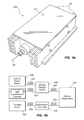
FIG. 6 a is a top perspective view of an exemplary embodiment of a multilayer SNAP device 200. FIG. 6 a shows optical fiber 50, coaxial connectors 90, and thermal housing 120. In the exemplary embodiment shown the detector is mounted inside an adiabatic demagnetization refrigerator and cooled to ˜150 milliK for measurements of the SDE (defined as the probability of detecting a photon that has been coupled into the fiber) and dark count rate (DCR).
FIG. 6 b is a diagram of the optical components of an exemplary embodiment of a multilayer SNAP test system. FIG. 6 b shows an exemplary embodiment of a multilayer SNAP test device 200. FIG. 6 b shows tunable laser 500 which in the exemplary embodiment illustrated is a 1 mW laser tunable from (1520 nm to 1630 nm) through a computer controlled polarization controller. FIG. 6 b illustrates optical attenuators 520, set to provide a count rate of approximately 50,000 photons/sec. FIG. 6 b shows micro electro-mechanical system (MEMS) optical switch 530 used to switch between a power meter and the device under test. Before each measurement, the MEMS switch output was sent to the power meter for calibration of the number of photons per second incident on the detector, then switched to the device under test for measurement of the SDE.
FIG. 7 a is a plot showing the system detection efficiency (SDE) of an exemplary embodiment of a multilayer SNAP device as a function of bias current. In the exemplary embodiment shown in FIG. 7 a light of 1550 nanometers is used. An SDE of 85.7%±0.6% is measured for the exemplary embodiment shown.
FIG. 7 b is a plot showing the dark count rate (DCR) of an exemplary embodiment of a multilayer SNAP device. Conditions used for the measurements shown in FIG. 7 b are the same as those for the measurements shown in FIG. 7 a. For the exemplary embodiment shown the DCR is lower than 400 cps with a fiber coupled to the detector, which we attribute to stray blackbody radiation coupled into the fiber. Without a fiber coupled to the detector, the device exhibits a DCR of less than 0.1 cps. For the two detectors connected in parallel the switching current of 9.8 microamperes is approximately twice the switching current of a typical single-layer SN-SPD. From the bias dependence of the SDE, we find an avalanche current IAV ˜0.6×ISW. The device exhibits a broad plateau in SDE over 40% of the bias range between the avalanche current and the switching current.
Although the larger signal-to-noise ratio is a benefit of the SNAP architecture, stacking the two sections of the multilayer SNAP at orthogonal angles eliminates the polarization dependence of the SDE in the exemplary embodiment.
FIG. 8 a is a map of the single-photon detection efficiency (SDE) over the Poincaré sphere of an exemplary embodiment of a multilayer SNAP device. The SDE values at 1560 nm are shown in a color scale and indicate the variation in efficiency over the whole range of possible polarizations. In FIG. 8 a the horizontal and vertical axes represent the axial ratio (AR) where AR=(major axis)/(minor axis), ∈=cot(AR), and the tilt angle (θ) of the polarization ellipse of the electric field vector of the photon. Using this notation, the quantities 2∈ and 2θ represent latitude and longitude on the Poincaré sphere. The entire Poincaré sphere is mapped by −90°<2∈<90° and 0<2θ<360°.
FIG. 8 b is a map of the single-photon detection efficiency (SDE) over the Poincaré sphere of a standard superconducting nanowire single photon detector (SN-SPD) device. The standard single-layer SNSPD exemplifying the prior art is a single-layer SNSPD had a wire width of 120 nanometers and a pitch of 220 nanometers. The device was embedded in an optical stack consisting of (bottom to top) a gold mirror, a layer of sputtered SiO2, the tungsten silicide detector, a second layer of SiO2, and a sputtered layer of TiO2, with layer thicknesses optimized for absorption at 1550 nm. Note the difference in scales.
Comparing FIG. 8 a of multilayer SNAP device and FIG. 8 a of the SN-SPD device the multilayer SNAP device shows a variation of less than 2%, over the Poincaré sphere compared to the single-layer device, which shows a variation of approximately 16%.
FIG. 9 a is a plot of the maximum and minimum SDE over the Poincaré sphere of an exemplary embodiment of a multilayer SNAP device. The SDE reaches a peak of 87.7%±0.5% at 1540 nm, close to the design wavelength of 1550 nm. At shorter and longer wavelengths, the SDE decreases due to the effects of the optical stack.
FIG. 9 b is a plot of the ratio of the maximum to minimum SDE (SDEmax/SDEmin) as a function of wavelength for an Indium-Gallium-Arsenide (InGaAs) power meter and for an exemplary embodiment of a multilayer SNAP device. The ratio RDSE=(SDEmax/SDEmin) for the multilayer SNAP device (indicated by solid boxes) shows a minimum of 1.019 at 1560 nm and remains below 1.04 over the entire wavelength span from 1510 nm to 1630 nm. The fact that RsDE never reaches unity is attributed to the polarization dependence of the optical components of the measurement setup. To support this contention FIG. 9 b also shows the wavelength dependence of the ratio between the maximum and minimum power measured by an InGaAs power meter while scanning the polarization over the Poincaré sphere, indicated by the blue triangles in FIG. 9 b. The similarity in the polarization dependence of the components of the measurement setup (shown in FIG. 6 b) is indicated by the overlap of the triangles overlap with the squares within the error bars of the measurement over a wavelength range from 1520 nm to 1580 nm, indicating that the primary source of the small polarization dependence is the measurement setup and suggesting that the multilayer SNAP itself is polarization independent.
For applications requiring high repetition rates, the rise time, decay time, and dead time of the detector are important metrics. In the exemplary embodiment a bias current of 9 microamperes an amplified voltage pulse height of 600 millivolts is measured with a rise time of 8 nanoseconds, a 1/e decay time of 57 nanoseconds, and a dead time (during which the system detection efficiency is suppressed) of 38 nanoseconds as estimated from inter-arrival time measurements. The long rise and decay times are due to the large series inductor (490 in FIG. 5) being ten times the inductance of continuous meander pattern inductors (470 and 480 in FIG. 5), required to ensure stable operation of the SNAP. As a result of the long rise time, we measure a relatively large jitter of ˜465 picoseconds.
Although the measured jitter is large relative to that of typical SNSPDs, it is significantly smaller than that of other single photon detectors such as transition edge sensors (TESs), and comparable to the jitter of commercially available Si APDs. The jitter of 465 picoseconds is compatible with the measurement of multi-photon entangled states produced at a repetition rate of 80 MHz by a Ti:Sapphire mode-locked laser. The mulitlayerSNAP would also provide for a smaller coincidence window than a TES in a loophole-free test of the Bell inequality allowing a smaller distance between detectors and improvement in the system detection efficiency in such a measurement. The jitter of the mulitlayerSNAP may be reduced by reducing the value of the large inductor 490 in FIG. 5, which can be done by reducing the inductance of each individual nanowire continuous meander patterns 470 and 480 in FIG. 5. This can be accomplished using a “nested” SNAP geometry, in which the top and bottom continuous meander patterns are themselves SNAPs.
The extension of the SNAP nanowire architecture into three-dimensions represents a significant advancement in single-photon detector technology. Improvements in optical stack design and fabrication and the use of a higher-fill-factor nanowire continuous meander pattern should allow for an SDE approaching 100%. The significant reduction of the polarization dependence of the SDE will enhance the overall detection efficiency in experiments where the light is un-polarized and will eliminate the need for polarization controllers and wave-plates in experiments where the light is strongly polarized. Finally, stacking more than two layers may provide a route to obtaining detection efficiencies approaching 100% that are less wavelength dependent, which may be important for applications requiring high detection efficiency over a broad range of wavelengths.

Claims (26)

What is claimed is:
1. A microcircuit apparatus for detecting single photons without regard to polarity comprised of:
a base layer;
a first superconducting layer having a first superconducting nanowire patterned to form a first continuous meander pattern;
wherein said first continuous meander pattern is comprised of parallel line segments joined by curved segments;
a dielectric layer comprised of material wherein said dialectic layer is substantially transparent to a predetermined photon wavelength; and
a second superconducting layer having a second superconducting nanowire patterned to form a second continuous meander pattern wherein said second continuous meander pattern is comprised of parallel line segments joined by curved segments.
2. The apparatus of claim 1 wherein substantially all of said parallel line segments of said first continuous meander pattern are orthogonally oriented to said parallel line segments of said second continuous meander pattern.
3. The apparatus of claim 1 wherein said first superconducting nanowire and said second superconducting nanowire are comprised of an amorphous metal-metalloid alloy.
4. The apparatus of claim 3 wherein said amorphous metal-metalloid alloy is comprised of an alloy of tungsten and silicon.
5. The apparatus of claim 4 wherein said alloy of tungsten and silicon is comprised of 20 mole percent to 30 mole percent silicon.
6. The apparatus of claim 1 wherein said dielectric layer is comprised of a material selected from a group consisting of an oxide of silicon and a nitride of silicon.
7. The apparatus of claim 1 wherein said dielectric layer is comprised of a transparent material selected from a group consisting of an oxide, a nitride and a fluoride.
8. The apparatus of claim 1 wherein said dielectric layer is comprised of a semiconductor selected from a group consisting of silicon or germanium.
9. The apparatus of claim 1 wherein said predetermined photon wavelength is approximately 300 nanometers to 3,000 nanometers.
10. The apparatus of claim 1 wherein said predetermined photon wavelength is approximately between 800 nanometers and 2000 nanometers.
11. The apparatus of claim 1 wherein said predetermined photon wavelength is approximately 1050 nanometers and 1600 nanometers.
12. The apparatus of claim 1 wherein said predetermined photon wavelength is approximately 1800 nanometers and 2400 nanometers.
13. The apparatus of claim 1 wherein said predetermined photon wavelength is approximately between 2000 nanometers and 8000 nanometers.
14. The apparatus of claim 1 wherein said first superconducting nanowire layer and said second superconducting nanowire layer are connected in series to electrical inductor components having an inductance greater than the inductance of said first superconducting nanowire layer and said second superconducting nanowire layer.
15. The apparatus of claim 14 wherein said inductance of said inductor component is at least 8 times the inductance of said first superconducting nanowire layer and said second superconducting nanowire layer.
16. The apparatus of claim 1 which further includes one or more dielectric layers on said second superconducting nanowire layer.
17. The apparatus of claim 1 in which said base layer is deposited on one or more alternating layers of silicon oxide, and silicon nitride.
18. The apparatus of claim 17 in which said one or more alternating layers of silicon oxide, and silicon nitride are deposited on a mirror layer consisting of a metal.
19. The apparatus of claim 1 wherein the width and pitch of said continuous meander pattern of said first superconducting nanowire layer are substantially equivalent to the width and pitch of said continuous meander pattern of said second superconducting nanowire.
20. The apparatus of claim 1 wherein the width and pitch of said continuous nanowire meander pattern of said first superconducting nanowire layer are not equivalent to the width and pitch of said continuous meander pattern of said second superconducting nanowire.
21. The apparatus of claim 1 wherein the width of said first superconducting nanowire and said second superconducting nanowires is between 3 nanometers and 3000 nanometers.
22. The apparatus of claim 1 wherein the thickness of said dielectric layer is between 3 nanometers and 3000 nanometers.
23. The apparatus of claim 1 wherein a detection area produced by said first and said second continuous meander pattern is at least 125 square micrometers.
24. A method of making a microcircuit apparatus for detecting single photons without regard to polarity comprised of:
forming a base layer;
forming first superconducting layer on said base layer;
patterning said first superconducting layer to form a first continuous meander pattern on said base layer wherein said continuous meander pattern is comprised of a series of substantially parallel line segments joined by curved segments to form said continuous meander pattern;
selecting a dielectric material to correspond to a predetermined photon wavelength;
forming a dielectric layer comprised of said dielectric material wherein said dialectic layer is substantially transparent to a predetermined photon wavelength; and
maintaining said microcircuit apparatus in a chamber that has a temperature of below 5 Kelvin.
25. The method of claim 24 which further includes the step of forming a second superconducting layer on said dielectric layer.
26. The method of claim of 24 which further includes the step of patterning said second superconducting layer with a continuous meander pattern orthogonally oriented to said first continuous meander pattern.
US13/869,802 2012-04-26 2013-04-24 Efficient polarization independent single photon detector Active 2033-06-12 US9240539B2 (en)

Priority Applications (2)

Application Number Priority Date Filing Date Title
US13/869,802 US9240539B2 (en) 2012-04-26 2013-04-24 Efficient polarization independent single photon detector
US14/698,442 US9577175B1 (en) 2012-04-26 2015-04-28 Efficient polarization independent single photon detector

Applications Claiming Priority (2)

Application Number Priority Date Filing Date Title
US201261638675P 2012-04-26 2012-04-26
US13/869,802 US9240539B2 (en) 2012-04-26 2013-04-24 Efficient polarization independent single photon detector

Related Child Applications (1)

Application Number Title Priority Date Filing Date
US14/698,442 Continuation US9577175B1 (en) 2012-04-26 2015-04-28 Efficient polarization independent single photon detector

Publications (2)

Publication Number Publication Date
US20140087952A1 US20140087952A1 (en) 2014-03-27
US9240539B2 true US9240539B2 (en) 2016-01-19

Family

ID=50339437

Family Applications (2)

Application Number Title Priority Date Filing Date
US13/869,802 Active 2033-06-12 US9240539B2 (en) 2012-04-26 2013-04-24 Efficient polarization independent single photon detector
US14/698,442 Active 2034-02-22 US9577175B1 (en) 2012-04-26 2015-04-28 Efficient polarization independent single photon detector

Family Applications After (1)

Application Number Title Priority Date Filing Date
US14/698,442 Active 2034-02-22 US9577175B1 (en) 2012-04-26 2015-04-28 Efficient polarization independent single photon detector

Country Status (1)

Country Link
US (2) US9240539B2 (en)

Cited By (6)

* Cited by examiner, † Cited by third party
Publication number Priority date Publication date Assignee Title
US20140353476A1 (en) * 2011-12-23 2014-12-04 Technion Research & Development Foundation Ltd. Fiber optical superconducting nanowire single photon detector
US20170186933A1 (en) * 2015-12-29 2017-06-29 Kristen Ann Sunter Superconducting nanowire avalanche photodetectors with reduced current crowding
WO2021076177A1 (en) * 2019-10-18 2021-04-22 Massachusetts Institute Of Technology Impedance matched superconducting nanowire photodetector for single- and multi-photon detection
US11385099B1 (en) 2017-06-26 2022-07-12 SeeQC Inc. Integrated superconducting nanowire digital photon detector
US20220344563A1 (en) * 2021-04-27 2022-10-27 Microsoft Technology Licensing, Llc Interfacing with superconducting circuitry
US20230175887A1 (en) * 2018-05-01 2023-06-08 PsiQuantum Corp. Photon Number Resolving Superconducting Detector

Families Citing this family (23)

* Cited by examiner, † Cited by third party
Publication number Priority date Publication date Assignee Title
CN104091883A (en) * 2014-07-15 2014-10-08 中国科学院上海微系统与信息技术研究所 Superconductive nanowire single photon detector based on dielectric film reflector
US9490112B2 (en) * 2015-03-06 2016-11-08 Robert Francis McDermott, III System and method for characterizing ions using a superconducting transmission line detector
CN104752534B (en) * 2015-04-27 2016-09-14 南京大学 Superconducting nano-wire single-photon detector and preparation method thereof
CN104835905A (en) * 2015-05-27 2015-08-12 南京大学 Polarized nonsensitive efficient superconducting nanowire single photon detector
KR101811214B1 (en) * 2015-05-29 2017-12-22 고려대학교 세종산학협력단 Flexible pressure sensor using an amorphous metal, and flexible bimodal sensor for simultaneously sensing pressure and temperature
AT517438B1 (en) * 2015-07-07 2018-10-15 Alfred Dipl Ing Fuchs DEVICE AND METHOD FOR DETECTING RADIATION
CN106549097B (en) * 2015-09-17 2019-05-10 中国科学院上海微系统与信息技术研究所 Inhibit the superconducting nano-wire single-photon detector of polarization sensitivity
CN105374928A (en) * 2015-11-17 2016-03-02 天津大学 Superconducting fractal nanowire single-photon detector and preparation method thereof
CN105355774A (en) * 2015-11-26 2016-02-24 南京大学 Superconducting nanowire single-photon detector with high polarization extinction ratio and high efficiency
DE102016004001B4 (en) * 2016-04-07 2019-11-28 Forschungszentrum Jülich GmbH Device for the detection of electrons, ions and / or photons
CN106124046B (en) * 2016-06-07 2018-01-12 天津大学 A kind of Jitter emulation mode of superconducting nano-wire single-photon detector
CN106289515B (en) * 2016-07-19 2017-12-19 天津大学 A kind of superconducting nano-wire single-photon detector carried from gaining structure
GB2566411A (en) * 2016-08-26 2019-03-13 Halliburton Energy Services Inc Arrayed distributed temperature sensing using single-photon detectors
WO2018038739A1 (en) * 2016-08-26 2018-03-01 Daniel Joshua Stark Arrayed distributed acoustic sensing using single-photon detectors
WO2018038735A1 (en) * 2016-08-26 2018-03-01 Halliburton Energy Services, Inc. Cooled single-photon detector apparatus and methods
CN107507911B (en) * 2017-08-10 2019-07-26 中国科学院上海微系统与信息技术研究所 Superconducting nano-wire single-photon detector
CN110350077A (en) * 2018-04-03 2019-10-18 中国科学院上海微系统与信息技术研究所 Big polarization extinction ratio micro-nano fiber Coupled Superconducting nanowire single photon detector
CN109668631B (en) * 2018-12-11 2021-06-01 中国科学院光电技术研究所 Preparation method of large-area and low-cost superconducting nanowire single photon detector
US11441954B2 (en) 2019-01-30 2022-09-13 King Fahd University Of Petroleum And Minerals Method, system and apparatus for measuring rest time of superconducting nanowire
EP3764068B1 (en) * 2019-07-11 2023-11-29 Université de Genève Device and system for single photon detection using a plurality of superconducting detection means connected in parallel
US20220376162A1 (en) * 2019-09-22 2022-11-24 Technion Research & Development Foundation Limited Superconductor composites and devices comprising same
CN112345092B (en) * 2020-11-06 2022-09-27 天津大学 Superconducting nanowire single photon detector
CN112763061B (en) * 2021-01-07 2022-02-08 南京大学 Two-dimensional superconducting nanowire pixel array structure based on thermal coupling structure and imager

Citations (3)

* Cited by examiner, † Cited by third party
Publication number Priority date Publication date Assignee Title
US5532485A (en) * 1994-10-14 1996-07-02 Northrop Grumman Corp. Multispectral superconductive quantum detector
US6812464B1 (en) * 2000-07-28 2004-11-02 Credence Systems Corporation Superconducting single photon detector
US8872109B2 (en) * 2010-03-05 2014-10-28 National Institute Of Advanced Industrial Science And Technology High-speed particle detector for discriminating charge states of ions

Patent Citations (4)

* Cited by examiner, † Cited by third party
Publication number Priority date Publication date Assignee Title
US5532485A (en) * 1994-10-14 1996-07-02 Northrop Grumman Corp. Multispectral superconductive quantum detector
US6812464B1 (en) * 2000-07-28 2004-11-02 Credence Systems Corporation Superconducting single photon detector
US7049593B2 (en) * 2000-07-28 2006-05-23 Credence Systems Corporation Superconducting single photon detector
US8872109B2 (en) * 2010-03-05 2014-10-28 National Institute Of Advanced Industrial Science And Technology High-speed particle detector for discriminating charge states of ions

Non-Patent Citations (2)

* Cited by examiner, † Cited by third party
Title
Baek, Burm, "Superconducting . . . ", Appl. Phys. Lets., vol. 98, 251105 (2011).
Verma, V. B., et. al., "A Three Dimensional . . . ", Appl. Phys. Letts., vol. 101, p. 251114 (2012).

Cited By (10)

* Cited by examiner, † Cited by third party
Publication number Priority date Publication date Assignee Title
US20140353476A1 (en) * 2011-12-23 2014-12-04 Technion Research & Development Foundation Ltd. Fiber optical superconducting nanowire single photon detector
US9726536B2 (en) * 2011-12-23 2017-08-08 Technion Research And Development Foundation Limited Fiber optical superconducting nanowire single photon detector
US20170186933A1 (en) * 2015-12-29 2017-06-29 Kristen Ann Sunter Superconducting nanowire avalanche photodetectors with reduced current crowding
US10505094B2 (en) * 2015-12-29 2019-12-10 Massachusetts Institute Of Technology Superconducting nanowire avalanche photodetectors with reduced current crowding
US11385099B1 (en) 2017-06-26 2022-07-12 SeeQC Inc. Integrated superconducting nanowire digital photon detector
US11747196B1 (en) 2017-06-26 2023-09-05 SeeQC, Inc. Integrated superconducting nanowire digital photon detector
US20230175887A1 (en) * 2018-05-01 2023-06-08 PsiQuantum Corp. Photon Number Resolving Superconducting Detector
WO2021076177A1 (en) * 2019-10-18 2021-04-22 Massachusetts Institute Of Technology Impedance matched superconducting nanowire photodetector for single- and multi-photon detection
US11522115B2 (en) 2019-10-18 2022-12-06 Massachusetts Institute Of Technology Impedance matched superconducting nanowire photodetector for single- and multi-photon detection
US20220344563A1 (en) * 2021-04-27 2022-10-27 Microsoft Technology Licensing, Llc Interfacing with superconducting circuitry

Also Published As

Publication number Publication date
US9577175B1 (en) 2017-02-21
US20140087952A1 (en) 2014-03-27

Similar Documents

Publication Publication Date Title
US9240539B2 (en) Efficient polarization independent single photon detector
Verma et al. A three-dimensional, polarization-insensitive superconducting nanowire avalanche photodetector
Gibson et al. Tapered InP nanowire arrays for efficient broadband high-speed single-photon detection
US20130143744A1 (en) Superconducting nanowire avalanche photodetectors (snaps) with fast reset time
US8761848B2 (en) Nanowire-based detector
US7791065B2 (en) Ultrasensitive optical detector having a large temporal resolution and using a waveguide, and methods for producing said detector
US9121761B2 (en) Infrared detectors
US10302498B1 (en) Silicon nitride-carbon nanotube-graphene nanocomposite microbolometer IR detector
JP2008071908A (en) Superconductive photodetector
Sandall et al. Linear array of InAs APDs operating at 2 µm
Gu et al. Fractal-inspired, polarization-insensitive superconducting nanowire single-photon detectors
CN113340436B (en) Uncooled CMOS infrared detector
Erotokritou et al. Nano-optical photoresponse mapping of superconducting nanowires with enhanced near infrared absorption
CN113447148A (en) Infrared focal plane detector
CN113447143B (en) Thermal symmetry type infrared detector
CN113447150B (en) Infrared detector with microbridge structure
CN113720449B (en) Infrared detector based on CMOS (complementary Metal oxide semiconductor) process
CN113720466B (en) Infrared detector based on CMOS (complementary Metal oxide semiconductor) process
CN113447142A (en) Reinforced CMOS infrared detector
Shank et al. Infrared nanoantenna-coupled rectenna for energy harvesting
CN113432728A (en) Single-layer hollow infrared microbridge detector
CN113720472A (en) Infrared detector based on CMOS (complementary Metal oxide semiconductor) process
Fu et al. A UV to NIR Si Wavelength Sensor With Simple Geometry and Good Resolution
KR20210004536A (en) Vertical nanowire based photodetector having double absorption layer and manufacturing method thereof
CN113566982B (en) Infrared detector with microbridge structure

Legal Events

Date Code Title Description
AS Assignment

Owner name: GOVERNMENT OF THE UNITED STATES OF AMERICA, AS REP

Free format text: ASSIGNMENT OF ASSIGNORS INTEREST;ASSIGNORS:MARSILI, FRANCESCO;NAM, SAE WOO;VERMA, VARUN BOEHM;SIGNING DATES FROM 20140412 TO 20140428;REEL/FRAME:032869/0218

Owner name: GOVERNMENT OF THE UNITED STATES OF AMERICA, AS REP

Free format text: ASSIGNMENT OF ASSIGNORS INTEREST;ASSIGNOR:NAM, SAE WOO;REEL/FRAME:032869/0042

Effective date: 20140401

STCF Information on status: patent grant

Free format text: PATENTED CASE

MAFP Maintenance fee payment

Free format text: PAYMENT OF MAINTENANCE FEE, 4TH YEAR, LARGE ENTITY (ORIGINAL EVENT CODE: M1551); ENTITY STATUS OF PATENT OWNER: LARGE ENTITY

Year of fee payment: 4

FEPP Fee payment procedure

Free format text: MAINTENANCE FEE REMINDER MAILED (ORIGINAL EVENT CODE: REM.); ENTITY STATUS OF PATENT OWNER: LARGE ENTITY

FEPP Fee payment procedure

Free format text: 7.5 YR SURCHARGE - LATE PMT W/IN 6 MO, LARGE ENTITY (ORIGINAL EVENT CODE: M1555); ENTITY STATUS OF PATENT OWNER: LARGE ENTITY

MAFP Maintenance fee payment

Free format text: PAYMENT OF MAINTENANCE FEE, 8TH YEAR, LARGE ENTITY (ORIGINAL EVENT CODE: M1552); ENTITY STATUS OF PATENT OWNER: LARGE ENTITY

Year of fee payment: 8