US9164211B2 - Display apparatus capable of controlling light transmittance - Google Patents
Display apparatus capable of controlling light transmittance Download PDFInfo
- Publication number
- US9164211B2 US9164211B2 US13/765,816 US201313765816A US9164211B2 US 9164211 B2 US9164211 B2 US 9164211B2 US 201313765816 A US201313765816 A US 201313765816A US 9164211 B2 US9164211 B2 US 9164211B2
- Authority
- US
- United States
- Prior art keywords
- retarder
- display device
- polarizer
- display apparatus
- external light
- Prior art date
- Legal status (The legal status is an assumption and is not a legal conclusion. Google has not performed a legal analysis and makes no representation as to the accuracy of the status listed.)
- Active, expires
Links
- 238000002834 transmittance Methods 0.000 title claims description 44
- 230000003287 optical effect Effects 0.000 claims abstract description 20
- 239000000758 substrate Substances 0.000 claims description 51
- 230000010287 polarization Effects 0.000 claims description 27
- 230000000903 blocking effect Effects 0.000 claims description 8
- 238000007789 sealing Methods 0.000 claims description 4
- 239000010408 film Substances 0.000 description 67
- 239000010410 layer Substances 0.000 description 32
- 238000010586 diagram Methods 0.000 description 23
- 230000003111 delayed effect Effects 0.000 description 16
- 239000004973 liquid crystal related substance Substances 0.000 description 15
- 239000010409 thin film Substances 0.000 description 15
- 238000002161 passivation Methods 0.000 description 14
- 238000009413 insulation Methods 0.000 description 13
- 230000001934 delay Effects 0.000 description 11
- 239000004065 semiconductor Substances 0.000 description 10
- 238000000034 method Methods 0.000 description 9
- 239000006185 dispersion Substances 0.000 description 7
- 239000000463 material Substances 0.000 description 6
- 230000008569 process Effects 0.000 description 6
- PXHVJJICTQNCMI-UHFFFAOYSA-N Nickel Chemical compound [Ni] PXHVJJICTQNCMI-UHFFFAOYSA-N 0.000 description 5
- KDLHZDBZIXYQEI-UHFFFAOYSA-N Palladium Chemical compound [Pd] KDLHZDBZIXYQEI-UHFFFAOYSA-N 0.000 description 5
- XLOMVQKBTHCTTD-UHFFFAOYSA-N Zinc monoxide Chemical compound [Zn]=O XLOMVQKBTHCTTD-UHFFFAOYSA-N 0.000 description 5
- 230000008859 change Effects 0.000 description 5
- 238000004519 manufacturing process Methods 0.000 description 5
- 230000035515 penetration Effects 0.000 description 5
- BASFCYQUMIYNBI-UHFFFAOYSA-N platinum Chemical compound [Pt] BASFCYQUMIYNBI-UHFFFAOYSA-N 0.000 description 5
- 239000011575 calcium Substances 0.000 description 4
- 239000011651 chromium Substances 0.000 description 4
- 239000010931 gold Substances 0.000 description 4
- 229910003437 indium oxide Inorganic materials 0.000 description 4
- PJXISJQVUVHSOJ-UHFFFAOYSA-N indium(iii) oxide Chemical compound [O-2].[O-2].[O-2].[In+3].[In+3] PJXISJQVUVHSOJ-UHFFFAOYSA-N 0.000 description 4
- 239000011229 interlayer Substances 0.000 description 4
- 229910052745 lead Inorganic materials 0.000 description 4
- 239000012780 transparent material Substances 0.000 description 4
- 229910052779 Neodymium Inorganic materials 0.000 description 3
- 229910052791 calcium Inorganic materials 0.000 description 3
- 229910052804 chromium Inorganic materials 0.000 description 3
- 150000001875 compounds Chemical class 0.000 description 3
- 239000004020 conductor Substances 0.000 description 3
- 230000003247 decreasing effect Effects 0.000 description 3
- 230000014509 gene expression Effects 0.000 description 3
- 229910052737 gold Inorganic materials 0.000 description 3
- 229910052741 iridium Inorganic materials 0.000 description 3
- 229910052744 lithium Inorganic materials 0.000 description 3
- 239000011777 magnesium Substances 0.000 description 3
- 229910052759 nickel Inorganic materials 0.000 description 3
- 239000011368 organic material Substances 0.000 description 3
- 229910052763 palladium Inorganic materials 0.000 description 3
- 229910052697 platinum Inorganic materials 0.000 description 3
- 229910052709 silver Inorganic materials 0.000 description 3
- 229910045601 alloy Inorganic materials 0.000 description 2
- 239000000956 alloy Substances 0.000 description 2
- 229910052782 aluminium Inorganic materials 0.000 description 2
- -1 e.g. Substances 0.000 description 2
- 239000011521 glass Substances 0.000 description 2
- 238000002347 injection Methods 0.000 description 2
- 239000007924 injection Substances 0.000 description 2
- 229910010272 inorganic material Inorganic materials 0.000 description 2
- 239000011147 inorganic material Substances 0.000 description 2
- 239000012774 insulation material Substances 0.000 description 2
- 229910052749 magnesium Inorganic materials 0.000 description 2
- 229910052750 molybdenum Inorganic materials 0.000 description 2
- 230000000149 penetrating effect Effects 0.000 description 2
- 239000007787 solid Substances 0.000 description 2
- 238000003860 storage Methods 0.000 description 2
- 125000005504 styryl group Chemical group 0.000 description 2
- 239000011787 zinc oxide Substances 0.000 description 2
- OYPRJOBELJOOCE-UHFFFAOYSA-N Calcium Chemical compound [Ca] OYPRJOBELJOOCE-UHFFFAOYSA-N 0.000 description 1
- VYZAMTAEIAYCRO-UHFFFAOYSA-N Chromium Chemical compound [Cr] VYZAMTAEIAYCRO-UHFFFAOYSA-N 0.000 description 1
- WHXSMMKQMYFTQS-UHFFFAOYSA-N Lithium Chemical compound [Li] WHXSMMKQMYFTQS-UHFFFAOYSA-N 0.000 description 1
- FYYHWMGAXLPEAU-UHFFFAOYSA-N Magnesium Chemical compound [Mg] FYYHWMGAXLPEAU-UHFFFAOYSA-N 0.000 description 1
- OAICVXFJPJFONN-UHFFFAOYSA-N Phosphorus Chemical compound [P] OAICVXFJPJFONN-UHFFFAOYSA-N 0.000 description 1
- 239000004642 Polyimide Substances 0.000 description 1
- 229910052581 Si3N4 Inorganic materials 0.000 description 1
- VYPSYNLAJGMNEJ-UHFFFAOYSA-N Silicium dioxide Chemical compound O=[Si]=O VYPSYNLAJGMNEJ-UHFFFAOYSA-N 0.000 description 1
- XUIMIQQOPSSXEZ-UHFFFAOYSA-N Silicon Chemical compound [Si] XUIMIQQOPSSXEZ-UHFFFAOYSA-N 0.000 description 1
- BQCADISMDOOEFD-UHFFFAOYSA-N Silver Chemical compound [Ag] BQCADISMDOOEFD-UHFFFAOYSA-N 0.000 description 1
- GWEVSGVZZGPLCZ-UHFFFAOYSA-N Titan oxide Chemical compound O=[Ti]=O GWEVSGVZZGPLCZ-UHFFFAOYSA-N 0.000 description 1
- NRTOMJZYCJJWKI-UHFFFAOYSA-N Titanium nitride Chemical compound [Ti]#N NRTOMJZYCJJWKI-UHFFFAOYSA-N 0.000 description 1
- 239000000853 adhesive Substances 0.000 description 1
- 230000001070 adhesive effect Effects 0.000 description 1
- XAGFODPZIPBFFR-UHFFFAOYSA-N aluminium Chemical compound [Al] XAGFODPZIPBFFR-UHFFFAOYSA-N 0.000 description 1
- 230000003667 anti-reflective effect Effects 0.000 description 1
- 230000008901 benefit Effects 0.000 description 1
- 239000003990 capacitor Substances 0.000 description 1
- PMHQVHHXPFUNSP-UHFFFAOYSA-M copper(1+);methylsulfanylmethane;bromide Chemical compound Br[Cu].CSC PMHQVHHXPFUNSP-UHFFFAOYSA-M 0.000 description 1
- XCJYREBRNVKWGJ-UHFFFAOYSA-N copper(II) phthalocyanine Chemical compound [Cu+2].C12=CC=CC=C2C(N=C2[N-]C(C3=CC=CC=C32)=N2)=NC1=NC([C]1C=CC=CC1=1)=NC=1N=C1[C]3C=CC=CC3=C2[N-]1 XCJYREBRNVKWGJ-UHFFFAOYSA-N 0.000 description 1
- 230000007423 decrease Effects 0.000 description 1
- 239000002019 doping agent Substances 0.000 description 1
- 238000010291 electrical method Methods 0.000 description 1
- QZQVBEXLDFYHSR-UHFFFAOYSA-N gallium(III) oxide Inorganic materials O=[Ga]O[Ga]=O QZQVBEXLDFYHSR-UHFFFAOYSA-N 0.000 description 1
- PCHJSUWPFVWCPO-UHFFFAOYSA-N gold Chemical compound [Au] PCHJSUWPFVWCPO-UHFFFAOYSA-N 0.000 description 1
- RBTKNAXYKSUFRK-UHFFFAOYSA-N heliogen blue Chemical compound [Cu].[N-]1C2=C(C=CC=C3)C3=C1N=C([N-]1)C3=CC=CC=C3C1=NC([N-]1)=C(C=CC=C3)C3=C1N=C([N-]1)C3=CC=CC=C3C1=N2 RBTKNAXYKSUFRK-UHFFFAOYSA-N 0.000 description 1
- 230000005525 hole transport Effects 0.000 description 1
- AMGQUBHHOARCQH-UHFFFAOYSA-N indium;oxotin Chemical compound [In].[Sn]=O AMGQUBHHOARCQH-UHFFFAOYSA-N 0.000 description 1
- GKOZUEZYRPOHIO-UHFFFAOYSA-N iridium atom Chemical compound [Ir] GKOZUEZYRPOHIO-UHFFFAOYSA-N 0.000 description 1
- 239000011159 matrix material Substances 0.000 description 1
- 238000010297 mechanical methods and process Methods 0.000 description 1
- 229910052751 metal Inorganic materials 0.000 description 1
- 239000002184 metal Substances 0.000 description 1
- 239000000203 mixture Substances 0.000 description 1
- IBHBKWKFFTZAHE-UHFFFAOYSA-N n-[4-[4-(n-naphthalen-1-ylanilino)phenyl]phenyl]-n-phenylnaphthalen-1-amine Chemical compound C1=CC=CC=C1N(C=1C2=CC=CC=C2C=CC=1)C1=CC=C(C=2C=CC(=CC=2)N(C=2C=CC=CC=2)C=2C3=CC=CC=C3C=CC=2)C=C1 IBHBKWKFFTZAHE-UHFFFAOYSA-N 0.000 description 1
- QEFYFXOXNSNQGX-UHFFFAOYSA-N neodymium atom Chemical compound [Nd] QEFYFXOXNSNQGX-UHFFFAOYSA-N 0.000 description 1
- TWNQGVIAIRXVLR-UHFFFAOYSA-N oxo(oxoalumanyloxy)alumane Chemical compound O=[Al]O[Al]=O TWNQGVIAIRXVLR-UHFFFAOYSA-N 0.000 description 1
- 230000000737 periodic effect Effects 0.000 description 1
- 238000000053 physical method Methods 0.000 description 1
- 229910021420 polycrystalline silicon Inorganic materials 0.000 description 1
- 229920000728 polyester Polymers 0.000 description 1
- 229920001721 polyimide Polymers 0.000 description 1
- 229920000642 polymer Polymers 0.000 description 1
- 230000004044 response Effects 0.000 description 1
- 229910052710 silicon Inorganic materials 0.000 description 1
- 239000010703 silicon Substances 0.000 description 1
- HQVNEWCFYHHQES-UHFFFAOYSA-N silicon nitride Chemical compound N12[Si]34N5[Si]62N3[Si]51N64 HQVNEWCFYHHQES-UHFFFAOYSA-N 0.000 description 1
- 229910052814 silicon oxide Inorganic materials 0.000 description 1
- 239000004332 silver Substances 0.000 description 1
- 239000002356 single layer Substances 0.000 description 1
- OGIDPMRJRNCKJF-UHFFFAOYSA-N titanium oxide Inorganic materials [Ti]=O OGIDPMRJRNCKJF-UHFFFAOYSA-N 0.000 description 1
- TVIVIEFSHFOWTE-UHFFFAOYSA-K tri(quinolin-8-yloxy)alumane Chemical compound [Al+3].C1=CN=C2C([O-])=CC=CC2=C1.C1=CN=C2C([O-])=CC=CC2=C1.C1=CN=C2C([O-])=CC=CC2=C1 TVIVIEFSHFOWTE-UHFFFAOYSA-K 0.000 description 1
- 238000001771 vacuum deposition Methods 0.000 description 1
- YVTHLONGBIQYBO-UHFFFAOYSA-N zinc indium(3+) oxygen(2-) Chemical compound [O--].[Zn++].[In+3] YVTHLONGBIQYBO-UHFFFAOYSA-N 0.000 description 1
Images


Classifications
-
- H—ELECTRICITY
- H10—SEMICONDUCTOR DEVICES; ELECTRIC SOLID-STATE DEVICES NOT OTHERWISE PROVIDED FOR
- H10K—ORGANIC ELECTRIC SOLID-STATE DEVICES
- H10K59/00—Integrated devices, or assemblies of multiple devices, comprising at least one organic light-emitting element covered by group H10K50/00
- H10K59/50—OLEDs integrated with light modulating elements, e.g. with electrochromic elements, photochromic elements or liquid crystal elements
-
- G—PHYSICS
- G02—OPTICS
- G02B—OPTICAL ELEMENTS, SYSTEMS OR APPARATUS
- G02B5/00—Optical elements other than lenses
- G02B5/30—Polarising elements
-
- G—PHYSICS
- G02—OPTICS
- G02B—OPTICAL ELEMENTS, SYSTEMS OR APPARATUS
- G02B5/00—Optical elements other than lenses
- G02B5/30—Polarising elements
- G02B5/3083—Birefringent or phase retarding elements
-
- H01L27/3232—
-
- H01L27/326—
-
- H01L51/5281—
-
- H—ELECTRICITY
- H10—SEMICONDUCTOR DEVICES; ELECTRIC SOLID-STATE DEVICES NOT OTHERWISE PROVIDED FOR
- H10K—ORGANIC ELECTRIC SOLID-STATE DEVICES
- H10K50/00—Organic light-emitting devices
- H10K50/80—Constructional details
- H10K50/86—Arrangements for improving contrast, e.g. preventing reflection of ambient light
-
- H—ELECTRICITY
- H10—SEMICONDUCTOR DEVICES; ELECTRIC SOLID-STATE DEVICES NOT OTHERWISE PROVIDED FOR
- H10K—ORGANIC ELECTRIC SOLID-STATE DEVICES
- H10K59/00—Integrated devices, or assemblies of multiple devices, comprising at least one organic light-emitting element covered by group H10K50/00
- H10K59/10—OLED displays
- H10K59/12—Active-matrix OLED [AMOLED] displays
- H10K59/121—Active-matrix OLED [AMOLED] displays characterised by the geometry or disposition of pixel elements
-
- H—ELECTRICITY
- H10—SEMICONDUCTOR DEVICES; ELECTRIC SOLID-STATE DEVICES NOT OTHERWISE PROVIDED FOR
- H10K—ORGANIC ELECTRIC SOLID-STATE DEVICES
- H10K59/00—Integrated devices, or assemblies of multiple devices, comprising at least one organic light-emitting element covered by group H10K50/00
- H10K59/80—Constructional details
- H10K59/8791—Arrangements for improving contrast, e.g. preventing reflection of ambient light
-
- H—ELECTRICITY
- H10—SEMICONDUCTOR DEVICES; ELECTRIC SOLID-STATE DEVICES NOT OTHERWISE PROVIDED FOR
- H10K—ORGANIC ELECTRIC SOLID-STATE DEVICES
- H10K59/00—Integrated devices, or assemblies of multiple devices, comprising at least one organic light-emitting element covered by group H10K50/00
- H10K59/80—Constructional details
- H10K59/8793—Arrangements for polarized light emission
-
- H01L2251/5323—
-
- H—ELECTRICITY
- H10—SEMICONDUCTOR DEVICES; ELECTRIC SOLID-STATE DEVICES NOT OTHERWISE PROVIDED FOR
- H10K—ORGANIC ELECTRIC SOLID-STATE DEVICES
- H10K2102/00—Constructional details relating to the organic devices covered by this subclass
- H10K2102/301—Details of OLEDs
- H10K2102/302—Details of OLEDs of OLED structures
- H10K2102/3023—Direction of light emission
- H10K2102/3031—Two-side emission, e.g. transparent OLEDs [TOLED]
Definitions
- an organic light-emitting display apparatus Since an organic light-emitting display apparatus has excellent characteristics in terms of viewing angles, contrast, response speeds, and power consumption, an application range of the organic light-emitting display apparatus has been increased from a personal portable device, e.g., a MP3 player or a mobile phone, to a TV. Such an organic light-emitting display device has a self-emission characteristic and does not require a separate light source, e.g., unlike a liquid crystal display device. Thus, thickness and weight of the organic light-emitting display device may be decreased.
- the organic light-emitting display device may be configured as a transparent display device by forming a transparent thin film transistor or a transparent organic light-emitting diode therein and forming a transmissive region (transmissive window) separately from a pixel region.
- Example embodiments provide a low power display apparatus with a light transmittance control by using a minimal number of elements of a transparent display device.
- the first polarizer and the second polarizer may have polarization axes in a same direction.
- the first and second phases may have same absolute values and different rotation directions, and when a location of the pattern retarder is adjusted to have the third retarder correspond to the second region of the transparent display device, the display apparatus may transmit the external light.
- the first and second phases may have same absolute values and different rotation directions, and when a location of the pattern retarder is adjusted to have the second retarder correspond to the second region of the transparent display device, the display apparatus may block the external light.
- the first polarizer and the second polarizer may have polarization axes perpendicular to each other.
- the first and second phases may have same absolute values and different rotation directions, and when a location of the pattern retarder is adjusted to have the second retarder correspond to the second region of the transparent display device, the display apparatus may transmit the external light.
- the first and second regions of the transparent display device may be alternately arranged in a vertical direction, the second and third retarders of the pattern retarder corresponding to the first and second regions.
- the display apparatus may further include a location changing unit configured to move the pattern retarder up or down by a half of a pixel pitch.
- the first and second regions of the transparent display device may be alternately arranged in a horizontal direction, the second and third retarders of the pattern retarder corresponding to the first and second regions.
- the display apparatus may further include a location changing unit configured to move the pattern retarder left or right by a half of a pixel pitch.
- Slow axes of the second and third retarders may be perpendicular to each other.
- a sum of a number of second retarders and a number of third retarders in the pattern retarder may be greater by one than twice a number of second regions in the transparent display device.
- the number of second retarders may be different by one than the number of third retarders.
- a display apparatus capable of controlling light transmittance, the display apparatus including a transparent display device including first and second regions, the first region being configured to display images, the second region being configured to transmit external light therethrough, and the first and second regions being adjacent to each other and being alternately arranged in a first direction, a first circular polarizer in an optical path of light emitted by the transparent display device, the first circular polarizer being configured to delay and circularly polarize a wavelength of the external light by a first phase, and a second circular polarizer opposite to the optical path emitted by the transparent display device, the second circular polarizer including a first delay region for delaying the external light by the first phase and a second delay region for delaying the external light by a second phase, the first and second delay regions being alternately arranged in the first direction, and the second circular polarizer being configured to delay and circularly polarize the wavelength of the external light by the first phase or the second phase.
- the first and second phases may have same absolute values and different rotation directions
- the first circular polarizer and the second circular polarizer may have polarization axes perpendicular to each other
- the display apparatus may further include a location changing unit for blocking or transmitting the external light by adjusting relative locations of the second circular polarizer and the transparent display device to have the first or second delay region of the second circular polarizer correspond to the second region the transparent display device.
- a display apparatus capable of controlling light transmittance, the display apparatus including a transparent display device including a first substrate with pixels and a second substrate sealing the first substrate, each pixel including first and second regions, the first region being configured to display images, the second region being configured to transmit external light therethrough, and the first and second regions being adjacent to each other and being alternately arranged in a first direction, a first linear polarizer on a first surface of the transparent display device, a first retarder between the first linear polarizer and the first surface of the transparent display device to delay the external light by a first phase, a second linear polarizer on a second surface of the transparent display device, the second surface being opposite the first surface, and a pattern retarder between the second polarizer and the second surface of the transparent display device, the pattern retarder including a second retarder for delaying a wavelength of the external light by a second phase and a third retarder for delaying the wavelength by a third phase, the second and third retarders being alternate
- the first and second phases may be the same, and the first and third phases may have same absolute values and different rotation directions.
- the first polarizer and the second polarizer may have polarization axes in a same direction, and the display apparatus may further include a location changing unit for blocking or transmitting the external light by adjusting relative locations of the pattern retarder and the transparent display device to have the second or third retarder correspond to the second region of the transparent display device.
- the first polarizer and the second polarizer may have polarization axes perpendicular to each other, and the display apparatus may further include a location changing unit for blocking or transmitting the external light by adjusting relative locations of the pattern retarder and the transparent display device to have the second or third retarder correspond to the second region the transparent display device.
- the first and second regions of the transparent display device may have patterns alternately repeated in a horizontal or vertical direction, and the second and third retarders of the pattern retarder may have patterns alternately arranged in a same direction as the first and second regions of the transparent display device.
- the first retarder may be between the second substrate and the first polarizer, and the pattern retarder may be between the first substrate and the second polarizer.
- FIG. 1 illustrates a schematic cross-sectional view of a display apparatus according to an embodiment
- FIG. 2 illustrates a schematic plane view of a transparent display device of FIG. 1 ;
- FIG. 3 illustrates a schematic plane view of a pattern retarder of FIG. 1 ;
- FIGS. 4 and 5 illustrate diagrams of pixels in the transparent display device of FIG. 1 ;
- FIG. 6 illustrates a cross-sectional view of a sub-pixel in the transparent device of FIG. 1 ;
- FIG. 7 illustrates a schematic cross-sectional view of a display apparatus according to another embodiment
- FIGS. 8 and 9 illustrate diagrams of pixels included in a transparent display device of FIG. 7 ;
- FIG. 10 illustrates a cross-sectional view of a sub-pixel in FIGS. 8 and 9 ;
- FIG. 11 illustrates a schematic diagram of an operation of a display apparatus according to an embodiment
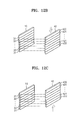
- FIGS. 12A through 12C illustrate diagrams of a relative location change of a transparent display device and a pattern retarder of FIG. 11 ;
- FIG. 13 illustrates a schematic diagram of an operation of a display apparatus according to another embodiment
- FIGS. 14A through 14C illustrates diagrams of a relative location change of a transparent display device and a pattern retarder of FIG. 13 ;
- FIGS. 15 through 18 illustrate diagrams of a transmittance of external light of a display apparatus according to a combination of a polarizing plate and a retarder according to an embodiment
- FIG. 19 illustrates a schematic diagram of an operation of a display apparatus according to another embodiment.
- the term “and/or” includes any and all combinations of one or more of the associated listed items. Expressions such as “at least one of,” when preceding a list of elements, modify the entire list of elements and do not modify the individual elements of the list.
- FIG. 1 is a schematic cross-sectional view of a display apparatus 100 according to an embodiment.
- the display apparatus 100 may include a first polarizer 51 , a first retarder 41 , a pattern retarder 42 , and a second polarizer 52 on a transparent display device 10 through which external light penetrates.
- the transparent display device 10 is a bottom emission-type organic light-emitting display apparatus and may include a first substrate 1 , a display unit disposed on the first substrate 1 , and a second substrate 2 sealing the display unit.
- the display unit is divided into a plurality of pixels between the first and second substrates 1 and 2 .
- one pixel is illustrated in FIG. 6 .
- Each pixel may include a pixel region 31 emitting light toward the first substrate 1 , i.e., a region displaying a generated image, and a transmissive region 32 adjacent to the pixel region 31 , i.e., a region through which external light penetrates.
- FIG. 2 is a schematic plan view of the transparent display device 10 of FIG. 1 .
- the display unit of the transparent display device 10 may include a plurality of pixels that are arranged in a matrix shape in row and column directions.
- the pixels are arranged such that the pixel region 31 and the transmissive region 32 of the transparent display device 10 have a pattern that alternately repeats in one direction.
- sub pixels may be arranged horizontally to define horizontal lines spaced apart from each other vertically, i.e., lines of the pixel regions 31 , so each transmissive region 32 may be between two pixel regions 31 to define an alternating pattern.
- the pixel region 31 and the transmissive region 32 are regularly formed at regular intervals in one direction in the transparent display device 10 .
- the first retarder 41 and the first polarizer 51 are sequentially disposed outside the first substrate 1 , e.g., the first substrate 1 may be between the second substrate 2 and the first retarder 41 , so light generated in or transmitted through the transparent display device 10 is emitted toward and passes through the first retarder 41 and the first polarizer 51 .
- Light passing through the first polarizer 51 and the first retarder 41 is circularly polarized in a predetermined direction.
- the first polarizer 51 and the first retarder 41 are stacked, i.e., directly disposed on top of each other, only left circularly polarized light or only right circularly polarized light passes through the combined first polarizer 51 and first retarder 41 , thereby enabling a user to clearly view an image by reducing reflection of the external light on an entire surface of the display apparatus 100 .
- the first polarizer 51 is a linear polarizer that linearly polarizes incident light in a predetermined direction
- the first retarder 41 is a retarder that delays a phase of an incident light by (+1/4) wavelength (+ ⁇ /4).
- the first retarder 41 converts linearly polarized light from into a circularly polarized light, or converts a circularly polarized light to a linearly polarized light.
- the first retarder 41 may be adhered to the transparent display device 10 via an adhesive material, or may be adhered to the transparent display device 10 in a film shape.
- the pattern retarder 42 and the second polarizer 52 are sequentially disposed outside the second substrate 2 , e.g., the second substrate 2 may be between the first substrate 1 and the pattern retarder 42 .
- the second polarizer 52 is a linear polarizer that linearly polarizes incident light in a predetermined direction.
- the pattern retarder 42 is a switchable retarder including a second retarder 421 that delays a phase of an incident light by ( ⁇ 1/4) wavelength ( ⁇ /4), and a third retarder 422 that delays a phase of an incident light by (+1/4) wavelength (+ ⁇ /4).
- the pattern retarder 42 converts linearly polarized light into circularly polarized light, or converts circularly polarized light to linearly polarized light.
- FIG. 3 is a schematic view of the pattern retarder 42 of FIG. 1 .
- the pattern retarder 42 may include repeatedly alternating second retarders 421 and third retarders 422 .
- the alternating pattern of the second and third retarders 421 and 422 may be in a same direction as the repeated pattern direction of the pixel regions 31 and the transmissive regions 32 of the transparent display device 10 .
- the second and third retarders 421 and 422 may alternate along the vertical direction ( FIG. 3 ), while the pixel and transmissive regions 31 and 32 may alternate along the vertical direction as well ( FIG. 2 ).
- transmittance of external light may be controlled by adjusting a relative location of the pattern retarder 42 in the transparent display device 10 , e.g., the pattern retarder 42 may be adjusted to have the second or third retarder 421 or 422 correspond to a periodic transmissive region 32 of the transparent display device 10 .
- the pattern retarder 42 may be adjusted to have either the second retarders 421 or the third retarders 422 overlap respective transmissive regions 32 of the transparent display device 10 , thereby controlling light transmittance.
- a sum of a number of the second retarders 421 and a number of the third retarders 422 in the pattern retarder 42 may be greater by one than twice a number of lines of the transmissive regions 32 of the transparent display device 10 .
- the number of the second retarders 421 may be greater by one than the number of the third retarders 422
- the number of the third retarders 422 may be greater by one than the number of the second retarders 421 .
- the transparent display device 10 may include five lines of transmissive regions 32 ( FIG.
- the pattern retarder 42 may include five second retarders 421 and six third retarders 422 ( FIG. 3 ), i.e., eleven retarders total.
- the number of pixels and retarders shown in FIGS. 2 and 3 is for convenience of description, and is not limited thereto.
- the pattern retarder 42 may have a structure including an alignment film and a liquid crystal film.
- the alignment film aligns liquid crystal molecules of the liquid crystal film, and may be formed of any suitable photo-alignment compound.
- the liquid crystal molecules of the liquid crystal film are aligned according to an alignment of the alignment film.
- the pattern retarder 42 having a periodically changing phase delay value may be formed by changing an alignment state of the liquid crystal molecules by varying an alignment process of the alignment film at regions where the second or third retarders 421 or 422 are located.
- the second and third retarders 421 and 422 may have slow axes that are perpendicular to each other.
- the first polarizer 51 and the second polarizer 52 may have the same polarization axes or different polarization axes.
- the display apparatus 100 is capable of converting the transmittance of the external light with low power via phase delay value control of the pattern retarder 42 .
- An embodiment provides the display apparatus 100 with various optical elements, i.e., the first polarizer 51 , the first retarder 41 , the pattern retarder 42 , and the second polarizer 52 , so transmittance of the external light may be adjusted by using the various optical elements.
- a liquid crystal may be disposed on one side of the transparent display device 10
- two glass substrates may be required to seal the liquid crystal.
- glass substrates and a liquid crystal may not be required due to a specific arrangement of the pattern retarder 42 and the various optical elements, so transmittance of the display apparatus 100 may be adjusted with low power.
- a wavelength dispersion of a liquid crystal e.g., the pattern retarder 42
- a wavelength dispersion of an optical element e.g., the first retarder 41
- a wavelength dispersion denotes a phenomenon where light of all wavelengths does not turn into a uniform black state or into a uniform transparent state.
- a solid type pattern retarder 42 i.e., a retarder with a plurality of repeatedly arranged retarders having different phase delay
- transmittance of external light may be increased when the display apparatus 100 is in a transparent mode, and may be decreased when the display apparatus 100 is in a black mode.
- adjusting transmittance of external light using the liquid crystal may conventionally require a liquid crystal sealing process and a transparent display device manufacturing process that are not performed separately, thereby providing a complex overall manufacturing process.
- transmittance of external light may be conventionally adjusted by adjusting an arrangement of the liquid crystal via an electrical method, thereby increasing process complexity.
- the overall manufacturing processes may be simplified.
- transmittance of external light may be simply adjusted by changing location of the pattern retarder 42 , e.g., relative to the transmissive regions 32 , via a mechanical/physical method.
- a user at a first side may view an image at an opposite side of the display device, i.e., outside the second substrate 2 , through a first external light 61 that penetrates from outside the second substrate 2 through the second substrate 2 and the first substrate 1 to the first side.
- a user at the second side may view an image at the first side of the display through a second external light 62 that penetrates from the first side through the first and second substrates 1 and 2 to the second side.
- the first external light 61 is an external light emitted in a same direction as an image
- the second external light 62 is an external light emitted in an opposite direction of the first external light 61 .
- the display apparatus 100 is in a black mode of no light penetration, the user at the first side is unable to view an image outside the second substrate 2 , and the user at the second side is unable to view the image outside the first substrate 1 .
- FIG. 4 is a diagram of a pixel included in the transparent display device 10 of FIG. 1 , according to an embodiment
- FIG. 5 is a diagram of a pixel according to another embodiment.
- the transmissive region 32 through which the external light penetrates is adjacent to the pixel region 31 .
- respective transmissive regions 32 may be independently disposed, e.g., to be separated from each other, according to the red, green, and blue sub-pixels Pr, Pg, and Pb, as shown in FIG. 4 .
- respective transmissive regions 32 may be connected to each other throughout the red, green, and blue sub-pixels Pr, Pg, and Pb, as shown in FIG. 5 .
- the pixel may include the plurality of pixel regions 31 spaced apart from each other along common transmissive regions 32 throughout the display unit. According to the embodiment of FIG.
- the area of the transmissive region 32 through which the external light penetrate is increased, so transmittance of the entire display unit may be increased. It is noted that while FIG. 5 illustrates that all the transmissive regions 32 of the red, green, and blue sub-pixels Pr, Pg, and Pb are connected to each other, the transmissive regions 32 of any two adjacent sub-pixels from among the red, green, and blue sub-pixels Pr, Pg, and Pb may be connected to each other.
- a buffer film 211 may be formed on the first substrate 1 , and the pixel circuit including the thin film transistor TR may be formed on the buffer film 211 . Then, a semiconductor active layer 212 may be formed on the buffer film 211 .
- the buffer film 211 prevents penetration of impure elements and levels a surface of the first substrate 1 , and may be formed of any one of various materials performing such functions.
- the buffer film 211 may be formed of an inorganic material, e.g., silicon oxide, silicon nitride, silicon oxynitride, aluminum oxide, aluminum nitride, titanium oxide, or titanium nitride, an organic material, e.g., polyimide, polyester, or acryl, or a stacked structure thereof.
- the buffer film 211 is not an essential element, and may not be included as occasion demands.
- the semiconductor active layer 212 may be formed of, e.g., polycrystalline silicon, an oxide semiconductor, etc.
- the semiconductor active layer 212 may be a (In 2 O 3 )a(Ga 2 O 3 )b(ZnO)c layer (G-I—Z—O layer), wherein a, b, and c are respectively a real number satisfying a ⁇ 0, b ⁇ 0, and c>0.
- the semiconductor active layer 212 is formed of such an oxide semiconductor, light transmittance of the pixel circuit unit 311 in the pixel region 31 may be further increased, thereby increasing transmittance of the external light of the entire display unit.
- a gate insulation film 213 may be formed on the buffer film 211 to cover the semiconductor active layer 212 , and a gate electrode 214 may be formed on the gate insulation film 213 .
- An interlayer insulation film 215 may be formed on the gate insulation film 213 to cover the gate electrode 214 , and a source electrode 216 and a drain electrode 217 may be formed on the interlayer insulation film 215 to each contact the semiconductor active layer 212 through a contact hole.
- the structure of the thin film transistor TR is not limited to the one above, and any suitable structure may be applied to the thin film transistor TR.
- a passivation film 218 may be formed to cover the thin film transistor TR.
- the passivation film 218 may be a single insulation film or a plurality of insulation films having a leveled top surface.
- the passivation film 218 may be formed of an inorganic material and/or an organic material.
- the passivation film 218 may be formed to cover both the pixel region 31 and the transmissive region 32 .
- the passivation film 218 may include an opening (not shown) at a location corresponding to the transmissive region 32 so as to further improve transmittance of the external light in the transmissive region 32 .
- a first electrode 221 of the organic light-emitting device EL that is electrically connected to the thin film transistor TR may be formed on the passivation film 218 .
- the first electrode 221 may be formed in an independent island shape in each of all sub-pixels.
- the first electrode 221 may be located in the emissive unit 312 of the pixel region 31 and may be disposed to not overlap with the pixel circuit unit 311 .
- a pixel-defining film 219 formed of an organic and/or inorganic insulation material may be formed on the passivation film 218 .
- the pixel-defining film 219 may include a third opening 219 a covering an edge and exposing a center of the first electrode 221 .
- the pixel-defining film 219 may cover the pixel region 31 , e.g., the pixel-defining film 219 may at least cover the edge of the first electrode 221 instead of covering the entire pixel region 31 .
- the pixel-defining film 219 may include a second opening 219 b at a location corresponding to the transmissive region 32 , so transmittance of external light in the transmissive region 32 may be further increased.
- Both the passivation film 218 and the pixel-defining film 219 may include a transparent material.
- transmittance of external light in the transparent display device 10 may be further increased.
- An organic film 223 and a second electrode 222 may be sequentially stacked on the first electrode 221 exposed through the third opening 219 a .
- the second electrode 222 covers the organic film 223 and the pixel-defining film 219 by facing the first electrode 221 .
- the second electrode 222 is located in the pixel region 31 , e.g., the second electrode 222 is formed at least in the pixel region 31 , and may include a first opening 222 a at a location corresponding to the transmissive region 32 . Since the second electrode 222 is not located in the transmissive region 32 , transmittance of external light in the transmissive region 32 may be further increased.
- the first and second openings 222 a and 219 b may be connected to each other.
- a low molecular or polymer organic film may be used as the organic film 223 .
- a hole injection layer (HIL), a hole transport layer (HTL), an emission layer (EML), an electron transport layer (ETL), and an electron injection layer (EIL) may be stacked in a single or complex structure, and any suitable organic material, e.g., copper phthalocyanine (CuPc), N,N′-Di(naphthalene-1-yl)-N,N′-diphenyl-benzidine (NPB), and tris-8-hydroxy quinoline aluminum) (Alq3), may be used.
- the low molecular organic film may be formed by using a vacuum deposition method.
- the HIL, the HTL, the ETL, and the EIL are common layers, and may be commonly applied to red, green, and blue sub-pixels.
- the first electrode 221 functions as an anode and the second electrode 222 functions as a cathode, or vice versa.
- the first electrode 221 may be a transparent electrode
- the second electrode 222 may be a reflective electrode.
- the first electrode 221 may include a transparent conductive material, e.g., indium tin oxide (ITO), indium zinc oxide (IZO), zinc oxide (ZnO), or indium oxide (In2O3).
- FIG. 7 is a cross-sectional view schematically illustrating a display apparatus 200 according to another embodiment. Unlike the display apparatus 100 shown in FIG. 1 , the display apparatus 200 of FIG. 7 includes a transparent display device that is a top emission-type organic light-emitting display apparatus.
- the first retarder 41 and the first polarizer 51 are disposed outside the second substrate 2 that emits light, i.e., a generated image, from the transparent display device 10 .
- the pattern retarder 42 and the second polarizer 52 are disposed outside the first substrate 1 that does not emit light sequentially, i.e., does not emit a generated image, from the transparent display device 10 . Since functions of other elements are substantially the same to those shown in FIGS. 1 through 3 , descriptions thereof are not provided.
- the user at the side where an image is realized may view an image outside the first substrate 1 through the first external light 61 that penetrates from outside the first substrate 1 to outside the second substrate 2 .
- the user at the side opposite to the side where an image is realized may also view an image outside the second substrate 2 through the second external light 62 that penetrates from outside the second substrate 2 to outside first substrate 1 .
- the first external light 61 is an external light emitted in the same direction as an image
- the second external light 62 is an external light emitted in an opposite direction of the first external light 61 .
- the user at the side where an image is realized is unable to view an image outside the first substrate 1 .
- the user at the side opposite to the side where the image is realized is also unable to view the image outside the second substrate 2 .
- FIG. 8 is a diagram of a pixel included in the transparent display device 10 of FIG. 7 , according to an embodiment of the example embodiments
- FIG. 9 is a diagram of a pixel according to another embodiment of the example embodiments.
- the pixels shown in FIGS. 8 and 9 are disposed such that the pixel circuit unit 311 and the emissive unit 312 included in the pixel region 31 overlap each other. Since the emissive unit 312 emits light in the direction of the second substrate 2 , the pixel circuit unit 311 and the emissive unit 312 may overlap with each other. In addition, as the emissive unit 312 covers the pixel circuit unit 311 including the pixel circuit, optical interference by the pixel circuit may be prevented. Since functions of other elements are substantially the same to those of FIGS. 4 and 5 , descriptions thereof are not provided.
- the transmissive regions 32 may be independently included according to the red, green, and blue sub-pixels Pr, Pg, and Pb, as shown in FIG. 8 , or may be connected to each other throughout the red, green, and blue sub-pixels Pr, Pg, and Pb, as shown in FIG. 9 .
- FIG. 10 is a cross-sectional view of any one of the red, green, and blue sub-pixels Pr, Pg, and Pb of FIGS. 8 and 9 .
- the thin film transistor TR is disposed in the pixel circuit unit 311
- the organic light-emitting device EL is disposed in the emissive unit 312 .
- the buffer film 211 may be formed on the first substrate 1 , the semiconductor active layer 212 may be formed on the buffer film 211 , and the gate insulation film 213 , the gate electrode 214 , and the interlayer insulation film 215 may be formed on the semiconductor active layer 212 .
- the source and drain electrodes 216 and 217 may be formed on the interlayer insulation film 215 .
- the passivation film 218 i.e., a type of insulation film, may be formed to cover the thin film transistor TR.
- the passivation film 218 may be formed to cover both the pixel region 31 and the transmissive region 32 .
- the passivation film 218 may include an opening (not shown) at a location corresponding to the transmissive region 32 , thereby further increasing transmittance of external light through the transmissive region 32 .
- the first electrode 221 of the organic light-emitting device EL that is electrically connected to the thin film transistor TR may be formed on the passivation film 218 .
- the first electrode 221 may be located at the emissive unit 312 in the pixel region 31 and may be disposed to cover the pixel circuit unit 311 by overlapping with the pixel circuit unit 311 .
- Both the passivation film 218 and the pixel-defining film 219 may include a transparent material.
- transmittance of external light through the transparent display device 10 may be further increased.
- the first electrode 221 may have a stacked structure of a transparent conductive material and a reflective film, and the second electrode 222 may be an anti-reflective and anti-transmissive electrode.
- the transparent conductive material may be, e.g., ITO, IZO, ZnO, or In 2 O 3 , which has a high work function.
- the reflective film may include at least one metal of, e.g., Ag, Mg Al, Pt, Pd, Au, Ni, Nd Ir, Cr, Li, Ca, Mo, and alloys thereof.
- the first electrode 221 may be formed in the pixel region 31 .
- FIG. 11 is a diagram for schematically describing an operation of a display apparatus 300 , according to an embodiment.
- the display apparatus 300 may be an electronic apparatus for processing and displaying an image, e.g., a tablet computer, a media storage apparatus, a mobile phone, or a personal portable terminal.
- the display apparatus 300 may include the first polarizer 51 , the first retarder 41 , the transparent display device 10 , the pattern retarder 42 , and the second polarizer 52 .
- the display apparatus 300 shown in FIG. 11 may be the display apparatus 100 or 200 shown in FIG. 1 or 7 .
- the display apparatus 300 may further include a controller 70 and a location changing unit 80 .
- descriptions about elements corresponding to those of FIGS. 1 and 7 are not provided.
- the transparent display device 10 may have a pattern in which the pixel region 31 and the transmissive region 32 are repeatedly and alternately arranged in a column direction (y-axis).
- the pattern retarder 42 may have a pattern in which the second retarder 421 and the third retarder 422 are repeatedly arranged in the column direction according to the pixel region 31 and the transmissive region 32 of the transparent display device 10 , e.g., the pixel regions 31 overlap the third retarders 422 and the transmissive regions 32 overlap the second retarders 421 .
- the controller 70 may include a driver integrated circuit (IC) (not shown) for driving the transparent display device 10 .
- the driver IC may include a scan driver applying scan signals to a plurality of scan lines S, and a data driver applying data signals to a plurality of data lines D.
- the scan and data lines S and D may be formed on the display unit of the transparent display device 10 .
- the controller 70 may output a control signal for controlling the transmittance of the external light to the location changing unit 80 .
- FIGS. 12A through 12C are diagrams for describing a relative location change of the transparent display device 10 and the pattern retarder 42 of FIG. 11 . Alternate long and short chain lines of FIGS. 12A through 12C are illustrated to describe a location correspondence relationship of the transparent display device 10 and the pattern retarder 42 .
- the pattern retarder 42 may be moved down by a predetermined distance as shown in FIG. 12B , or may be moved up by a predetermined distance as shown in FIG. 12C , such that the second retarder 421 delaying the phase of the incident light of the pattern retarder 42 by ( ⁇ /4) may be disposed to correspond to the pixel region 31 of the transparent display device 10 , and the third retarder 422 delaying the phase of the incident light by (+ ⁇ /4) may be disposed to correspond to the transmissive region 32 of the transparent display device 10 .
- the second retarder 421 delaying the phase of the incident light by ( ⁇ /4) may be disposed to correspond to the pixel region 31 of the transparent display device 10
- the third retarder 422 delaying the phase of the incident light by (+ ⁇ /4) may be disposed to correspond to the transmissive region 32 of the transparent display device 10
- the pattern retarder 42 may be moved up or down by a predetermined distance to adjust the third retarder 422 to correspond to the pixel region 31 of the transparent display device 10
- the second retarder 421 d to correspond to the transmissive region 32 of the transparent display device 10 .
- FIG. 13 is a diagram for schematically describing an operation of a display apparatus 400 , according to another embodiment.
- the display apparatus 400 of FIG. 13 includes the transparent display device 10 with the pixel region 31 and the transmissive region 32 repeatedly arranged in a row direction (x-axis). Therefore, the pattern retarder 42 has a pattern in which the second retarder 421 and the third retarder 422 are repeatedly arranged in the row direction according to the pixel region 31 and the transmissive region 32 of the transparent display device 10 .
- FIGS. 14A through 14C are diagrams for describing a relative location change of the transparent display device 10 and the pattern retarder 42 of FIG. 13 . Alternate long and short chain lines of FIGS. 14A through 14C are illustrated to describe a location correspondence relationship of the transparent display device 10 and the pattern retarder 42 .
- the pattern retarder 42 is arranged to have the third retarder 422 , i.e., which delays the phase of the incident light by (+ ⁇ /4), correspond to the pixel region 31 of the transparent display device 10 , and the second retarder 421 , i.e., which delays the phase of the incident light by ( ⁇ /4), correspond to the transmissive region 32 of the transparent display device 10 .
- the display apparatus 400 may move the pattern retarder 42 left by a predetermined distance, as shown in FIG. 14B , or right by a predetermined distance, as shown in FIG. 14C , by using the location changing unit 80 . As such, the horizontal movement of the pattern retarder 42 sets the second retarder 421 to correspond to the pixel region 31 of the transparent display device 10 , and the third retarder 422 to correspond to the transmissive region 32 of the transparent display device 10 .
- the second retarder 421 delaying the phase of the incident light by ( ⁇ /4) may be disposed to correspond to the pixel region 31 of the transparent display device 10
- the third retarder 422 delaying the phase of the incident light by (+ ⁇ /4) may be disposed to correspond to the transmissive region 32 of the transparent display device 10 .
- the pattern retarder 42 may be moved left or right by a predetermined distance such that the third retarder 422 delaying the phase of the incident light by (+ ⁇ /4) may be disposed to correspond to the pixel region 31 of the transparent display device 10 , and the second retarder 421 delaying the phase of the incident light by ( ⁇ /4) may be disposed to correspond to the transmissive region 32 of the transparent display device 10 .
- FIGS. 15 and 16 are diagrams describing adjustment of transmittance of external light of a display apparatus according to example embodiments.
- FIGS. 15 and 16 are described by using light proceeding in a direction opposite to a direction of an image, i.e., the second external light 62 incident on a front surface of the display apparatus, and light proceeding in the same direction as the direction of the image, i.e., the first external light 61 incident on the rear surface of the display apparatus.
- FIG. 15 is a diagram describing adjustment of transmittance of external light of a display apparatus according to a relative location relationship of the transparent display device 10 and the pattern retarder 42 shown in FIG. 12A or 14 A.
- the relative locations of the transparent display device 10 and the pattern retarder 42 are controlled such that the second retarder 421 of the pattern retarder 42 delaying the phase of the incident light by ( ⁇ 1/4) wavelength ( ⁇ /4) corresponds to the transmissive region 32 of the transparent display device 10 .
- the first retarder 41 is a retarder that delays an incident light by (+1/4) wavelength (+ ⁇ /4). Accordingly, the first retarder 41 and the second retarder 421 of the pattern retarder 42 delay the light by opposite phases, i.e., same absolute values but different directions.
- the first polarizer 51 and the second polarizer 52 have polarization axes in the same direction.
- the second external light 62 that passes through the first polarizer 51 is linearly polarized and emerges from the first polarizer 51 as linearly polarized second external light 62 a .
- the linearly polarized light passes through the first retarder 41 and emerges as external light 62 b having a phase delayed by (+1/4) wavelength (+ ⁇ /4).
- external light 62 b passes through the transmissive region 32 of the transparent display device 10 and through the second retarder 421 of the pattern retarder 42 and emerges as external light 62 c having a phase delayed by ( ⁇ 1/4) wavelength ( ⁇ /4).
- external light 62 c passes through the second polarizer 52 to be linearly polarized and emerge as external light 62 d.
- the first external light 61 is incident on the second polarizer 52 and is linearly polarized to emerge from the second polarizer 52 as external light 61 a .
- the external light 61 a passes through the second retarder 421 of the pattern retarder 42 to emerge as external light 61 b having a phase delayed by ( ⁇ 1/4) wavelength ( ⁇ /4).
- the external light 61 b passes through the transmissive region 32 of the transparent display device 10 and through the first retarder 41 to emerge as external light 61 c having a phase delayed by (+1/4) wavelength (+ ⁇ /4).
- the external light 61 c passes through the first polarizer 51 and is polarized to emerge as external light 61 d from the first polarizer 51 .
- a transparent mode of the display apparatuses 100 through 400 may be easily realized by determining a phase delay value of an external light penetrated through via location control of the pattern retarder 42 .
- the user may view an image via light emitted from the pixel region 31 of the transparent display device 10 .
- FIG. 16 is a diagram describing adjustment of transmittance of external light of a display apparatus according to a relative location relationship of the transparent display device 10 and the pattern retarder 42 shown in FIG. 12B , 12 C, 14 B, or 14 C.
- the relative locations of the transparent display device 10 and the pattern retarder 42 are controlled such that the third retarder 422 of the pattern retarder 42 delaying the phase of the incident light by (+1/4) wavelength (+ ⁇ /4) corresponds to the transmissive region 32 of the transparent display device 10 .
- the first retarder 41 is a retarder that delays an incident light by (+1/4) wavelength (+ ⁇ /4). Accordingly, the first retarder 41 and the third retarder 422 of the pattern retarder 42 delay the incident light by the same phase, i.e., same absolute values and direction.
- the first polarizer 51 and the second polarizer 52 have polarization axes in the same direction.
- the second external light 62 turns into external light 62 a that is linearly polarized by passing through the first polarizer 51 .
- the external light 62 a turns into external light 62 b having a phase delayed by (+1/4) wavelength (+ ⁇ /4) by passing through the first retarder 41 .
- the external light 62 b turns into external light 62 c having a phase delayed by (+1/4) wavelength (+ ⁇ /4) by passing through the transmissive region 32 of the transparent display device 10 and passing through the third retarder 422 of the pattern retarder 42 .
- the external light 62 c is linearly polarized in the same direction as the first polarizer 51 by passing through the second polarizer 52 , and is blocked.
- the first external light 61 turns into external light 61 a that is linearly polarized by passing through the second polarizer 52 .
- the external light 61 a turns into external light 61 b having a phase delayed by (+1/4) wavelength (+ ⁇ /4) by passing through the third retarder 422 of the pattern retarder 42 .
- the external light 61 b turns into external light 61 c having a phase delayed by (+1/4) wavelength (+ ⁇ /4) by passing through the transmissive region 32 of the transparent display device 10 and passing through the first retarder 41 .
- the external light 61 c is linearly polarized in the same direction as the second polarizer 52 by passing through the first polarizer 51 , and is blocked.
- a black mode of the display apparatuses 100 through 400 may be easily realized by determining a phase delay value of an external light penetrated through via location control of the pattern retarder 42 .
- the user may view an image via light emitted from the pixel region 31 of the transparent display device 10 .
- the first polarizer 51 and the second polarizer 52 have polarization axes in the same direction, and the relative locations of the transparent display device 10 and the pattern retarder 42 are controlled by physically moving the pattern retarder 42 .
- the display apparatuses 100 through 400 may be easily switched between the transparent mode and the black mode.
- FIGS. 17 and 18 are diagrams for describing adjustment of transmittance of external light of a display apparatus according to a combination of a polarizing plate and a retarder, according to another embodiment of the example embodiments.
- FIGS. 17 and 18 are described by using light proceeding in a direction opposite to a direction of an image, i.e., the second external light 62 , and light proceeding in the same direction as the direction of the image, i.e., the first external light 61 .
- FIG. 17 is a diagram for describing adjusting of a transmittance of external light of a display apparatus according to a relative location relationship of the transparent display device 10 and the pattern retarder 42 shown in FIG. 12A or 14 A.
- the relative locations of the transparent display device 10 and the pattern retarder 42 are controlled such that the second retarder 421 of the pattern retarder 42 delaying the phase of the incident light by ( ⁇ 1/4) wavelength ( ⁇ /4) corresponds to the transmissive region 32 of the transparent display device 10 .
- the first retarder 41 is a retarder that delays an incident light by (+1/4) wavelength (+ ⁇ /4). Accordingly, the first retarder 41 and the second retarder 421 of the pattern retarder 42 delay the incident light by opposite phases, i.e., by the same absolute values but different directions.
- a polarization axis of the first polarizer 51 is perpendicular to a polarization axis of the second polarizer 52 .
- the second external light 62 turns into external light 62 a that is linearly polarized by passing through the first polarizer 51 .
- the external light 62 a turns into the external light 62 b having a phase delayed by (+1/4) wavelength (+ ⁇ /4) by passing through the first retarder 41 .
- the external light 62 b turns into external light 62 c having a phase delayed by ( ⁇ 1/4) wavelength ( ⁇ /4) by passing through the transmissive region 32 of the transparent display device 10 and passing through the second retarder 421 of the pattern retarder 42 .
- the external light 62 c is linearly polarized in a direction different from the first polarizer 51 by passing through the second polarizer 52 , and is blocked.
- the first external light 61 turns into external light 61 a that is linearly polarized by passing through the second polarizer 52 .
- the external light 61 a turns into external light 61 b having a phase delayed by ( ⁇ 1/4) wavelength ( ⁇ /4) by passing through the second retarder 421 of the pattern retarder 42 .
- the external light 61 b turns into external light 61 c having a phase delayed by (+1/4) wavelength (+ ⁇ /4) by passing through the transmissive region 32 of the transparent display device 10 and passing through the first retarder 41 .
- the external light 61 c is linearly polarized in a direction different from the second polarizer 52 by passing through the first polarizer 51 , and is blocked.
- a black mode of the display apparatuses 100 through 400 may be easily realized by determining a phase delay value of an external light penetrated through via location control of the pattern retarder 42 .
- the user may view an image via light emitted from the pixel region 31 of the transparent display device 10 .
- FIG. 18 is a diagram for describing adjusting of transmittance of external light of a display apparatus according to a relative location relationship of the transparent display device 10 and the pattern retarder 42 shown in FIG. 12B , 12 C, 14 B, or 14 C.
- the relative locations of the transparent display device 10 and the pattern retarder 42 are controlled such that the third retarder 422 of the pattern retarder 42 delaying the phase of the incident light by (+1/4) wavelength (+ ⁇ /4) corresponds to the transmissive region 32 of the transparent display device 10 .
- the first retarder 41 is a retarder that delays an incident light by (+1/4) wavelength (+ ⁇ /4). Accordingly, the first retarder 41 and the third retarder 422 of the pattern retarder 42 delay the incident light by the same phase, i.e., same absolute values and direction.
- the polarization axis of the first polarizer 51 is perpendicular to the polarization axis of the second polarizer 52 .
- the second external light 62 turns into the external light 62 a that is linearly polarized by passing through the first polarizer 51 .
- the external light 62 a turns into the external light 62 b having a phase delayed by (+1/4) wavelength (+ ⁇ /4) by passing through the first retarder 41 .
- the external light 62 b turns into the external light 62 c having a phase delayed by (+1/4) wavelength (+ ⁇ /4) by passing through the transmissive region 32 of the transparent display device 10 and passing through the third retarder 422 of the pattern retarder 42 .
- the external light 62 c turns into the external light 62 d by being linearly polarized in a different direction from the first polarizer 51 by passing through the second polarizer 52 .
- the first external light 61 turns into the external light 61 a that is linearly polarized by passing through the second polarizer 52 .
- the external light 61 a turns into the external light 61 b having a phase delayed by (+1/4) wavelength (+ ⁇ /4) by passing through the third retarder 422 of the pattern retarder 42 .
- the external light 61 b turns into the external light 61 c having a phase delayed by (+1/4) wavelength (+ ⁇ /4) by passing through the transmissive region 32 of the transparent display device 10 and passing through the first retarder 41 .
- the external light 61 c turns into the external light 61 d by being linearly polarized in a different direction from the second polarizer 52 by passing through the first polarizer 51 .
- a transparent mode of the display apparatuses 100 through 400 may be easily realized by determining a phase delay value of an external light penetrated through via location control of the pattern retarder 42 .
- the user may view an image via light emitted from the pixel region 31 of the transparent display device 10 .
- the first polarizer 51 and the second polarizer 52 have polarization axes perpendicular to each other, and the relative locations of the transparent display device 10 and the pattern retarder 42 are controlled by physically moving the pattern retarder 42 .
- the display apparatuses 100 through 400 may be easily switched between the transparent mode and the black mode.
- FIG. 19 is a diagram for schematically describing an operation of a display apparatus 500 according to another embodiment.
- the display apparatus 500 may include a first circular polarizer 71 disposed on an optical path emitted by the transparent display device 10 , and a second circular polarizer 72 disposed opposite to the optical path emitted by the transparent display device 10 .
- the first circular polarizer 71 replaces a combination of the first retarder 41 and the first polarizer 51 of any one of the display apparatuses 100 through 400 described above
- the second circular polarizer 72 replaces a combination of the pattern retarder 42 and the second polarizer 52 . Since functions and operations of other elements are substantially the same to those of the display apparatuses 100 through 400 described above, descriptions thereof are not provided.
- the first circular polarizer 71 circularly polarizes incident light by delaying a phase of the incident light by (+1/4) wavelength (+ ⁇ /4).
- the second circular polarizer 72 has a polarization axis that is the same as or perpendicular to the first circular polarizer 71 and has a pattern in which a first delay region delaying a phase of an incident light by ( ⁇ 1/4) wavelength ( ⁇ /4) and a second delay region delaying the phase of the incident light by (+1/4) wavelength (+ ⁇ /4) are repeatedly arranged.
- the first and second delay regions may have perpendicular slow axes.
- the display apparatus 500 may move the second circular polarizer 72 up and down or left and right by using the location changing unit 80 , such that the first or second delay region corresponds to the transmissive region 32 of the transparent display device 10 . Therefore, the display apparatus 500 transmits or blocks the external light of the display apparatus 500 .
- the display apparatus 500 of FIG. 19 may be manufactured by reducing two processes of disposing a retarder and a linear polarizer to one process of disposing a circular polarizer. Also, processes are simplified by adjusting an anti-reflection (AR) characteristic of the circular polarizer without having to separately adjust an AR characteristic of a retarder.
- AR anti-reflection
- optical elements may be organized outside, i.e., on outer surfaces of, a transparent display device, thereby controlling transmittance of external light therethrough with low power and minimized number of optical elements. Accordingly, the display apparatus may have a decreased weight, a reduced number of manufacturing processes, reduced material costs, and reduced defection rate. Further, transmittance in the transparent display device increases in a transparent mode and decreases in a black mode.
Landscapes
- Physics & Mathematics (AREA)
- Optics & Photonics (AREA)
- General Physics & Mathematics (AREA)
- Geometry (AREA)
- Engineering & Computer Science (AREA)
- Microelectronics & Electronic Packaging (AREA)
- Electroluminescent Light Sources (AREA)
- Devices For Indicating Variable Information By Combining Individual Elements (AREA)
- Polarising Elements (AREA)
Applications Claiming Priority (2)
| Application Number | Priority Date | Filing Date | Title |
|---|---|---|---|
| KR10-2012-0061081 | 2012-06-07 | ||
| KR1020120061081A KR101338250B1 (ko) | 2012-06-07 | 2012-06-07 | 광투과율 제어가 가능한 표시장치 |
Publications (2)
| Publication Number | Publication Date |
|---|---|
| US20130329288A1 US20130329288A1 (en) | 2013-12-12 |
| US9164211B2 true US9164211B2 (en) | 2015-10-20 |
Family
ID=48325402
Family Applications (1)
| Application Number | Title | Priority Date | Filing Date |
|---|---|---|---|
| US13/765,816 Active 2033-09-23 US9164211B2 (en) | 2012-06-07 | 2013-02-13 | Display apparatus capable of controlling light transmittance |
Country Status (6)
| Country | Link |
|---|---|
| US (1) | US9164211B2 (enExample) |
| EP (1) | EP2672541A3 (enExample) |
| JP (1) | JP2013254734A (enExample) |
| KR (1) | KR101338250B1 (enExample) |
| CN (1) | CN103489891B (enExample) |
| TW (1) | TWI580026B (enExample) |
Cited By (6)
| Publication number | Priority date | Publication date | Assignee | Title |
|---|---|---|---|---|
| US20160238881A1 (en) * | 2015-02-13 | 2016-08-18 | Samsung Display Co., Ltd. | Liquid crystal display apparatus and method of manufacturing the same |
| US9905622B2 (en) | 2014-08-27 | 2018-02-27 | Boe Technology Group Co., Ltd. | Organic electroluminescent device and manufacturing method thereof, each having a display apparatus |
| US20180067232A1 (en) * | 2016-01-28 | 2018-03-08 | Boe Technology Group Co., Ltd. | Anti-Reflection Structure and Fabrication Method Thereof, Display Device and Fabrication Method Thereof |
| US20230030096A1 (en) * | 2021-08-02 | 2023-02-02 | Samsung Display Co., Ltd. | Display apparatus, electronic device including the same, and method of manufacturing the display apparatus |
| US11665950B2 (en) | 2018-03-16 | 2023-05-30 | Fujifilm Corporation | Electroluminescent display device |
| US12217644B2 (en) | 2016-07-04 | 2025-02-04 | Samsung Display Co., Ltd. | Organic light emitting display panel |
Families Citing this family (58)
| Publication number | Priority date | Publication date | Assignee | Title |
|---|---|---|---|---|
| WO2011137429A2 (en) | 2010-04-30 | 2011-11-03 | Arizona Board Of Regents Acting For And On Behalf Of Arizona State University | Synthesis of four coordinated palladium complexes and their applications in light emitting devices thereof |
| TWI558713B (zh) | 2011-04-14 | 2016-11-21 | 美國亞利桑那州立大學董事會 | 吡啶-氧苯基配位之銥(iii)錯合物及其製造及使用方法 |
| WO2012162488A1 (en) | 2011-05-26 | 2012-11-29 | Arizona Board Of Regents Acting For And On Behalf Of Arizona State University | Synthesis of platinum and palladium complexes as narrow-band phosphorescent emitters for full color displays |
| KR102124227B1 (ko) | 2012-09-24 | 2020-06-17 | 아리조나 보드 오브 리젠츠 온 비하프 오브 아리조나 스테이트 유니버시티 | 금속 화합물, 방법, 및 이의 용도 |
| WO2014109814A2 (en) | 2012-10-26 | 2014-07-17 | Arizona Board Of Regents Acting For And On Behalf Of Arizona State University | Metal complexes, methods, and uses thereof |
| JP6804823B2 (ja) | 2013-10-14 | 2020-12-23 | アリゾナ・ボード・オブ・リージェンツ・オン・ビハーフ・オブ・アリゾナ・ステイト・ユニバーシティーArizona Board of Regents on behalf of Arizona State University | 白金錯体およびデバイス |
| US10020455B2 (en) | 2014-01-07 | 2018-07-10 | Arizona Board Of Regents On Behalf Of Arizona State University | Tetradentate platinum and palladium complex emitters containing phenyl-pyrazole and its analogues |
| KR102160157B1 (ko) * | 2014-01-13 | 2020-09-28 | 삼성디스플레이 주식회사 | 유기 발광 표시 장치 및 유기 발광 표시 장치의 제조 방법 |
| TWI544228B (zh) * | 2014-04-21 | 2016-08-01 | 王仁宏 | 光學模組及用於光學裝置之光學功能膜 |
| US9941479B2 (en) | 2014-06-02 | 2018-04-10 | Arizona Board Of Regents On Behalf Of Arizona State University | Tetradentate cyclometalated platinum complexes containing 9,10-dihydroacridine and its analogues |
| US9923155B2 (en) | 2014-07-24 | 2018-03-20 | Arizona Board Of Regents On Behalf Of Arizona State University | Tetradentate platinum (II) complexes cyclometalated with functionalized phenyl carbene ligands and their analogues |
| PL3175493T3 (pl) * | 2014-07-31 | 2024-05-27 | Basf Coatings Gmbh | Struktura hermetyzacyjna dla wyświetlacza oled z właściwościami antyrefleksyjnymi |
| CN105336759B (zh) * | 2014-08-06 | 2018-06-29 | 上海和辉光电有限公司 | 显示面板 |
| WO2016025921A1 (en) | 2014-08-15 | 2016-02-18 | Arizona Board Of Regents On Behalf Of Arizona State University | Non-platinum metal complexes for excimer based single dopant white organic light emitting diodes |
| CN105353533B (zh) * | 2014-08-20 | 2019-11-12 | 群创光电股份有限公司 | 显示面板及使用其的显示设备 |
| US11329244B2 (en) | 2014-08-22 | 2022-05-10 | Arizona Board Of Regents On Behalf Of Arizona State University | Organic light-emitting diodes with fluorescent and phosphorescent emitters |
| KR102166502B1 (ko) * | 2014-09-16 | 2020-10-16 | 삼성디스플레이 주식회사 | 유기 발광 표시 장치 |
| KR102254582B1 (ko) | 2014-10-02 | 2021-05-24 | 삼성디스플레이 주식회사 | 유기 발광 표시 장치 및 그 제조 방법 |
| US10033003B2 (en) | 2014-11-10 | 2018-07-24 | Arizona Board Of Regents On Behalf Of Arizona State University | Tetradentate metal complexes with carbon group bridging ligands |
| US9865825B2 (en) | 2014-11-10 | 2018-01-09 | Arizona Board Of Regents On Behalf Of Arizona State University | Emitters based on octahedral metal complexes |
| KR102319689B1 (ko) * | 2015-05-07 | 2021-11-01 | 한화테크윈 주식회사 | 돔 카메라 시스템 |
| US9879039B2 (en) | 2015-06-03 | 2018-01-30 | Arizona Board Of Regents On Behalf Of Arizona State University | Tetradentate and octahedral metal complexes containing naphthyridinocarbazole and its analogues |
| US11930662B2 (en) | 2015-06-04 | 2024-03-12 | Arizona Board Of Regents On Behalf Of Arizona State University | Transparent electroluminescent devices with controlled one-side emissive displays |
| US10158091B2 (en) | 2015-08-04 | 2018-12-18 | Arizona Board Of Regents On Behalf Of Arizona State University | Tetradentate platinum (II) and palladium (II) complexes, devices, and uses thereof |
| US10576081B2 (en) * | 2015-08-20 | 2020-03-03 | Apple Inc. | Self-emissive display with switchable retarder for high contrast |
| US10230048B2 (en) * | 2015-09-29 | 2019-03-12 | X-Celeprint Limited | OLEDs for micro transfer printing |
| CN105259708B (zh) * | 2015-11-20 | 2018-09-14 | 武汉华星光电技术有限公司 | 透明显示器 |
| KR102416742B1 (ko) * | 2015-12-21 | 2022-07-06 | 삼성디스플레이 주식회사 | 투명 표시 장치 |
| JP6716913B2 (ja) * | 2015-12-25 | 2020-07-01 | 大日本印刷株式会社 | 光学機能層付カラーフィルタ基材 |
| KR102490627B1 (ko) * | 2015-12-31 | 2023-01-20 | 엘지디스플레이 주식회사 | 액정 표시 장치 및 그 구동방법 |
| KR102651055B1 (ko) * | 2016-03-24 | 2024-03-26 | 삼성디스플레이 주식회사 | 광학 필름 및 디스플레이 장치 |
| US11335865B2 (en) | 2016-04-15 | 2022-05-17 | Arizona Board Of Regents On Behalf Of Arizona State University | OLED with multi-emissive material layer |
| US11137641B2 (en) | 2016-06-10 | 2021-10-05 | X Display Company Technology Limited | LED structure with polarized light emission |
| WO2018003380A1 (ja) * | 2016-06-30 | 2018-01-04 | 富士フイルム株式会社 | 光学装置および表示装置 |
| US10505145B2 (en) * | 2016-07-26 | 2019-12-10 | Samsung Display Co., Ltd. | Display device |
| US10177323B2 (en) | 2016-08-22 | 2019-01-08 | Arizona Board Of Regents On Behalf Of Arizona State University | Tetradentate platinum (II) and palladium (II) complexes and octahedral iridium complexes employing azepine functional groups and their analogues |
| KR20210083134A (ko) | 2016-10-12 | 2021-07-06 | 아리조나 보드 오브 리젠츠 온 비하프 오브 아리조나 스테이트 유니버시티 | 협대역 적색 인광성 4좌 백금(ii) 착물 |
| JP2018073761A (ja) * | 2016-11-04 | 2018-05-10 | パイオニア株式会社 | 発光装置 |
| US11183670B2 (en) | 2016-12-16 | 2021-11-23 | Arizona Board Of Regents On Behalf Of Arizona State University | Organic light emitting diode with split emissive layer |
| US11708385B2 (en) | 2017-01-27 | 2023-07-25 | Arizona Board Of Regents On Behalf Of Arizona State University | Metal-assisted delayed fluorescent emitters employing pyrido-pyrrolo-acridine and analogues |
| CN106997931A (zh) * | 2017-03-29 | 2017-08-01 | 武汉华星光电技术有限公司 | Oled显示面板以及oled显示装置 |
| US11101435B2 (en) | 2017-05-19 | 2021-08-24 | Arizona Board Of Regents On Behalf Of Arizona State University | Tetradentate platinum and palladium complexes based on biscarbazole and analogues |
| US10516117B2 (en) | 2017-05-19 | 2019-12-24 | Arizona Board Of Regents On Behalf Of Arizona State University | Metal-assisted delayed fluorescent emttters employing benzo-imidazo-phenanthridine and analogues |
| US11647643B2 (en) | 2017-10-17 | 2023-05-09 | Arizona Board Of Regents On Behalf Of Arizona State University | Hole-blocking materials for organic light emitting diodes |
| US11594688B2 (en) | 2017-10-17 | 2023-02-28 | Arizona Board Of Regents On Behalf Of Arizona State University | Display and lighting devices comprising phosphorescent excimers with preferred molecular orientation as monochromatic emitters |
| US12037348B2 (en) | 2018-03-09 | 2024-07-16 | Arizona Board Of Regents On Behalf Of Arizona State University | Blue and narrow band green and red emitting metal complexes |
| US12091429B2 (en) | 2018-07-16 | 2024-09-17 | Arizona Board Of Regents On Behalf Of Arizona State University | Fluorinated porphyrin derivatives for optoelectronic applications |
| US11878988B2 (en) | 2019-01-24 | 2024-01-23 | Arizona Board Of Regents On Behalf Of Arizona State University | Blue phosphorescent emitters employing functionalized imidazophenthridine and analogues |
| US11594691B2 (en) | 2019-01-25 | 2023-02-28 | Arizona Board Of Regents On Behalf Of Arizona State University | Light outcoupling efficiency of phosphorescent OLEDs by mixing horizontally aligned fluorescent emitters |
| KR102778472B1 (ko) * | 2019-02-08 | 2025-03-12 | 삼성디스플레이 주식회사 | 표시 장치 및 그 제조방법 |
| WO2021010217A1 (ja) * | 2019-07-16 | 2021-01-21 | Agc株式会社 | 透明表示装置、合わせガラス、及び透明表示装置の製造方法 |
| US11785838B2 (en) | 2019-10-02 | 2023-10-10 | Arizona Board Of Regents On Behalf Of Arizona State University | Green and red organic light-emitting diodes employing excimer emitters |
| CN110752249B (zh) * | 2019-11-20 | 2022-08-09 | 京东方科技集团股份有限公司 | 显示装置及其控制方法,显示面板 |
| CN111312774A (zh) * | 2020-02-25 | 2020-06-19 | 武汉华星光电半导体显示技术有限公司 | 一种显示装置 |
| US11945985B2 (en) | 2020-05-19 | 2024-04-02 | Arizona Board Of Regents On Behalf Of Arizona State University | Metal assisted delayed fluorescent emitters for organic light-emitting diodes |
| KR20220006683A (ko) * | 2020-07-08 | 2022-01-18 | 삼성디스플레이 주식회사 | 표시 장치 |
| KR20220169518A (ko) * | 2021-06-18 | 2022-12-28 | 삼성디스플레이 주식회사 | 디스플레이 장치 및 그 제조방법 |
| KR20230159145A (ko) * | 2022-05-13 | 2023-11-21 | 동우 화인켐 주식회사 | 광투과율 제어가 가능한 표시장치 |
Citations (10)
| Publication number | Priority date | Publication date | Assignee | Title |
|---|---|---|---|---|
| KR100283275B1 (ko) | 1997-12-26 | 2001-03-02 | 마찌다 가쯔히꼬 | 액정 디스플레이 장치 |
| US20010055082A1 (en) * | 1997-12-26 | 2001-12-27 | Sharp Kabushiki Kaisha | Liquid crystal display device |
| KR20020064293A (ko) | 1999-09-28 | 2002-08-07 | 샤프 레버러토리즈 오브 유럽 리미티드 | 액정 디바이스 및 디스플레이 |
| JP2005114983A (ja) | 2003-10-07 | 2005-04-28 | Seiko Epson Corp | 液晶装置及び電子機器 |
| KR20050060847A (ko) | 2003-12-17 | 2005-06-22 | 삼성전자주식회사 | 액정 표시 장치와, 이의 광학 필름 어셈블리 |
| KR100518426B1 (ko) | 2003-03-27 | 2005-09-29 | 엘지.필립스 엘시디 주식회사 | 액정표시장치 |
| KR20070027918A (ko) | 2005-08-30 | 2007-03-12 | 엘지.필립스 엘시디 주식회사 | 반사투과형 횡전계 모드 액정표시장치 |
| US7920233B2 (en) | 2004-11-12 | 2011-04-05 | Merck Patent Gmbh | Transflective vertically aligned liquid crystal display with in-cell patterned quarter-wave retarder |
| US20120268696A1 (en) | 2011-04-25 | 2012-10-25 | Sang-Hoon Yim | Display apparatus and method of operating the same |
| US20120327331A1 (en) | 2011-06-27 | 2012-12-27 | Sang-Hoon Yim | Display apparatus for controlling optical transmissivity |
Family Cites Families (9)
| Publication number | Priority date | Publication date | Assignee | Title |
|---|---|---|---|---|
| GB8403092D0 (en) * | 1984-02-06 | 1984-03-07 | Gardner H I | Polarshade |
| US6835504B2 (en) * | 2002-05-13 | 2004-12-28 | Macronix International Co., Ltd. | Photomask with illumination control over patterns having varying structural densities |
| GB2403023A (en) * | 2003-06-20 | 2004-12-22 | Sharp Kk | Organic light emitting device |
| JP4316960B2 (ja) * | 2003-08-22 | 2009-08-19 | 株式会社半導体エネルギー研究所 | 装置 |
| WO2007063782A1 (en) * | 2005-11-30 | 2007-06-07 | Semiconductor Energy Laboratory Co., Ltd. | Display device |
| JP2007180024A (ja) * | 2005-11-30 | 2007-07-12 | Semiconductor Energy Lab Co Ltd | 表示装置 |
| TW200732733A (en) * | 2006-02-17 | 2007-09-01 | Ind Tech Res Inst | Hybrid display |
| US20100165275A1 (en) * | 2007-06-15 | 2010-07-01 | Michinori Tsukamoto | Optical element, display device, and optical device |
| KR20110101980A (ko) * | 2010-03-10 | 2011-09-16 | 삼성모바일디스플레이주식회사 | 유기 발광 표시 장치 및 그 제조방법 |
-
2012
- 2012-06-07 KR KR1020120061081A patent/KR101338250B1/ko active Active
-
2013
- 2013-02-13 US US13/765,816 patent/US9164211B2/en active Active
- 2013-03-11 TW TW102108482A patent/TWI580026B/zh active
- 2013-04-30 EP EP13165955.9A patent/EP2672541A3/en not_active Withdrawn
- 2013-05-24 CN CN201310198817.XA patent/CN103489891B/zh active Active
- 2013-05-31 JP JP2013115057A patent/JP2013254734A/ja active Pending
Patent Citations (13)
| Publication number | Priority date | Publication date | Assignee | Title |
|---|---|---|---|---|
| US20010055082A1 (en) * | 1997-12-26 | 2001-12-27 | Sharp Kabushiki Kaisha | Liquid crystal display device |
| KR100283275B1 (ko) | 1997-12-26 | 2001-03-02 | 마찌다 가쯔히꼬 | 액정 디스플레이 장치 |
| KR20020064293A (ko) | 1999-09-28 | 2002-08-07 | 샤프 레버러토리즈 오브 유럽 리미티드 | 액정 디바이스 및 디스플레이 |
| US6774977B1 (en) | 1999-09-28 | 2004-08-10 | Sharp Laboratories Of Europe Limited | Liquid crystal device and display |
| KR100518426B1 (ko) | 2003-03-27 | 2005-09-29 | 엘지.필립스 엘시디 주식회사 | 액정표시장치 |
| US7102715B2 (en) | 2003-03-27 | 2006-09-05 | Lg.Philips Lcd Co., Ltd. | Dual display liquid crystal display device, method of operating the same, and mobile communication terminal including the same |
| JP2005114983A (ja) | 2003-10-07 | 2005-04-28 | Seiko Epson Corp | 液晶装置及び電子機器 |
| US20050134773A1 (en) | 2003-12-17 | 2005-06-23 | Samsung Electronics, Co., Ltd. | Optical film assembly for a display device |
| KR20050060847A (ko) | 2003-12-17 | 2005-06-22 | 삼성전자주식회사 | 액정 표시 장치와, 이의 광학 필름 어셈블리 |
| US7920233B2 (en) | 2004-11-12 | 2011-04-05 | Merck Patent Gmbh | Transflective vertically aligned liquid crystal display with in-cell patterned quarter-wave retarder |
| KR20070027918A (ko) | 2005-08-30 | 2007-03-12 | 엘지.필립스 엘시디 주식회사 | 반사투과형 횡전계 모드 액정표시장치 |
| US20120268696A1 (en) | 2011-04-25 | 2012-10-25 | Sang-Hoon Yim | Display apparatus and method of operating the same |
| US20120327331A1 (en) | 2011-06-27 | 2012-12-27 | Sang-Hoon Yim | Display apparatus for controlling optical transmissivity |
Non-Patent Citations (1)
| Title |
|---|
| Korean Notice of Allowance dated Nov. 20, 2013. |
Cited By (11)
| Publication number | Priority date | Publication date | Assignee | Title |
|---|---|---|---|---|
| US9905622B2 (en) | 2014-08-27 | 2018-02-27 | Boe Technology Group Co., Ltd. | Organic electroluminescent device and manufacturing method thereof, each having a display apparatus |
| US20160238881A1 (en) * | 2015-02-13 | 2016-08-18 | Samsung Display Co., Ltd. | Liquid crystal display apparatus and method of manufacturing the same |
| US9891465B2 (en) * | 2015-02-13 | 2018-02-13 | Samsung Display Co., Ltd. | Liquid crystal display apparatus and method of manufacturing the same |
| US10534217B2 (en) | 2015-02-13 | 2020-01-14 | Samsung Display Co., Ltd. | Liquid crystal display apparatus and method of manufacturing the same |
| US20180067232A1 (en) * | 2016-01-28 | 2018-03-08 | Boe Technology Group Co., Ltd. | Anti-Reflection Structure and Fabrication Method Thereof, Display Device and Fabrication Method Thereof |
| US10684394B2 (en) * | 2016-01-28 | 2020-06-16 | Boe Technology Group Co., Ltd. | Anti-reflection structure and fabrication method thereof, display device and fabrication method thereof |
| US12217644B2 (en) | 2016-07-04 | 2025-02-04 | Samsung Display Co., Ltd. | Organic light emitting display panel |
| US11665950B2 (en) | 2018-03-16 | 2023-05-30 | Fujifilm Corporation | Electroluminescent display device |
| US20230030096A1 (en) * | 2021-08-02 | 2023-02-02 | Samsung Display Co., Ltd. | Display apparatus, electronic device including the same, and method of manufacturing the display apparatus |
| US11917862B2 (en) * | 2021-08-02 | 2024-02-27 | Samsung Display Co., Ltd. | Display apparatus, electronic device including the same, and method of manufacturing the display apparatus |
| US12382792B2 (en) | 2021-08-02 | 2025-08-05 | Samsung Display Co., Ltd. | Display apparatus, electronic device including the same, and method of manufacturing the display apparatus |
Also Published As
| Publication number | Publication date |
|---|---|
| CN103489891A (zh) | 2014-01-01 |
| EP2672541A2 (en) | 2013-12-11 |
| CN103489891B (zh) | 2017-10-24 |
| US20130329288A1 (en) | 2013-12-12 |
| KR101338250B1 (ko) | 2013-12-09 |
| EP2672541A3 (en) | 2016-09-14 |
| TW201401500A (zh) | 2014-01-01 |
| JP2013254734A (ja) | 2013-12-19 |
| TWI580026B (zh) | 2017-04-21 |
Similar Documents
| Publication | Publication Date | Title |
|---|---|---|
| US9164211B2 (en) | Display apparatus capable of controlling light transmittance | |
| US9634075B2 (en) | Organic light emitting display device | |
| US8854578B2 (en) | Display apparatus and method of operating the same | |
| US9709844B2 (en) | Display apparatus capable of controlling light transmittance and method of manufacturing the same | |
| JP6496365B2 (ja) | 発光装置 | |
| JP6054066B2 (ja) | 光透過率制御の可能な表示装置 | |
| US9391127B2 (en) | Display device for controlling light transmittance | |
| TWI573116B (zh) | 用以控制透光率之顯示裝置 | |
| US8963815B2 (en) | Organic light-emitting display device | |
| US8963129B2 (en) | Organic light emitting display device | |
| US8598582B2 (en) | Organic light emitting display device | |
| US20150144891A1 (en) | Organic light-emitting diode (oled) display capable of controlling light transmittance | |
| US11903267B2 (en) | Organic light-emitting display apparatus | |
| US20130328945A1 (en) | Display device and method of operating the same | |
| US9146418B2 (en) | Display device |
Legal Events
| Date | Code | Title | Description |
|---|---|---|---|
| AS | Assignment |
Owner name: SAMSUNG DISPLAY CO., LTD., KOREA, REPUBLIC OF Free format text: ASSIGNMENT OF ASSIGNORS INTEREST;ASSIGNORS:YIM, SANG-HOON;CHO, KWAN-HYUN;KIM, KYUNG-HO;AND OTHERS;REEL/FRAME:029803/0634 Effective date: 20130129 |
|
| FEPP | Fee payment procedure |
Free format text: PAYOR NUMBER ASSIGNED (ORIGINAL EVENT CODE: ASPN); ENTITY STATUS OF PATENT OWNER: LARGE ENTITY |
|
| STCF | Information on status: patent grant |
Free format text: PATENTED CASE |
|
| MAFP | Maintenance fee payment |
Free format text: PAYMENT OF MAINTENANCE FEE, 4TH YEAR, LARGE ENTITY (ORIGINAL EVENT CODE: M1551); ENTITY STATUS OF PATENT OWNER: LARGE ENTITY Year of fee payment: 4 |
|
| MAFP | Maintenance fee payment |
Free format text: PAYMENT OF MAINTENANCE FEE, 8TH YEAR, LARGE ENTITY (ORIGINAL EVENT CODE: M1552); ENTITY STATUS OF PATENT OWNER: LARGE ENTITY Year of fee payment: 8 |