US9136093B2 - Synchronization of RF pulsing with RF metrology, processing, and control - Google Patents
Synchronization of RF pulsing with RF metrology, processing, and control Download PDFInfo
- Publication number
- US9136093B2 US9136093B2 US13/761,955 US201313761955A US9136093B2 US 9136093 B2 US9136093 B2 US 9136093B2 US 201313761955 A US201313761955 A US 201313761955A US 9136093 B2 US9136093 B2 US 9136093B2
- Authority
- US
- United States
- Prior art keywords
- output
- driver
- module
- setpoint
- rail voltage
- Prior art date
- Legal status (The legal status is an assumption and is not a legal conclusion. Google has not performed a legal analysis and makes no representation as to the accuracy of the status listed.)
- Active
Links
Images


Classifications
-
- H—ELECTRICITY
- H01—ELECTRIC ELEMENTS
- H01J—ELECTRIC DISCHARGE TUBES OR DISCHARGE LAMPS
- H01J37/00—Discharge tubes with provision for introducing objects or material to be exposed to the discharge, e.g. for the purpose of examination or processing thereof
- H01J37/32—Gas-filled discharge tubes
- H01J37/32009—Arrangements for generation of plasma specially adapted for examination or treatment of objects, e.g. plasma sources
- H01J37/32082—Radio frequency generated discharge
- H01J37/32174—Circuits specially adapted for controlling the RF discharge
-
- H—ELECTRICITY
- H01—ELECTRIC ELEMENTS
- H01J—ELECTRIC DISCHARGE TUBES OR DISCHARGE LAMPS
- H01J37/00—Discharge tubes with provision for introducing objects or material to be exposed to the discharge, e.g. for the purpose of examination or processing thereof
- H01J37/32—Gas-filled discharge tubes
- H01J37/32917—Plasma diagnostics
- H01J37/3299—Feedback systems
Definitions
- the present disclosure relates to plasma chambers and to radio frequency (RF) measurement systems and methods.
- RF radio frequency
- a radio frequency (RF) generator receives alternating current (AC) input power and generates an RF output.
- the RF output may be applied to, for example, a plasma electrode of a plasma chamber.
- Plasma chambers may be used in thin film manufacturing systems and other types of systems.
- a plasma chamber may include a plurality of plasma electrodes.
- more than one plasma electrode may be implemented where a surface area being treated is larger than an area that a single plasma electrode may be capable servicing.
- Each of the RF generators generates an RF output and applies the RF output to one of the plasma electrodes.
- the RF generators may be electrically connected in an effort to generate identical RF outputs.
- a radio frequency (RF) system in a first feature, includes an RF sensor, an analog to digital converter (ADC) module, a processing module, and a synchronization module.
- the RF sensor measures a parameter of an RF output and generates an RF signal based on the parameter.
- the ADC module converts samples of the RF signal into digital values.
- the processing module generates processed values based on the digital values.
- the synchronization module outputs one of the processed values in response to a transition in the RF output.
- the RF system further includes: a driver that generates the RF output; a power supply module that applies a rail voltage to the driver based on a rail voltage setpoint; a driver control module that drives the driver based on a driver control setpoint; and an output control module that, based on the one of the processed values, selectively adjusts at least one of the rail voltage setpoint and the driver control setpoint.
- the ADC module samples the RF signal at a first predetermined frequency.
- the output control module selectively updates the rail voltage setpoint and the driver control setpoint at a second predetermined frequency.
- the second predetermined frequency is less than the first predetermined frequency.
- the synchronization module outputs the one of the processed values in response to an increase in the RF signal that is greater than a predetermined value.
- the synchronization module outputs the one of the processed values in response to a decrease in the RF signal that is greater than a predetermined value
- the synchronization module outputs the one of the processed values in response to one of an increase and a decrease in the rail voltage that is greater than a predetermined value.
- the synchronization module outputs the one of the processed values in response to one of an increase and a decrease in an output of the driver control module that is greater than a predetermined value.
- the RF sensor further measures a second parameter of the RF output and generates a second RF signal based on the second parameter
- the RF system further comprises a second ADC module that converts samples of the second RF signal into second digital values
- the processing module generates second processed values based on the second digital values
- the synchronization module outputs one of the second processed values in response to the transition in the RF output
- the output control module selectively adjusts at least one of the rail voltage setpoint and the driver control setpoint further based on the one of the second processed values.
- a plasma chamber system includes: the RF system; a filter that filters the RF output; and a plasma electrode that receives the filtered RF output.
- a radio frequency (RF) control method includes: measuring a parameter of an RF output using an RF sensor; generating an RF signal based on the parameter using the RF sensor; converting samples of the RF signal into digital values; generating processed values based on the digital values; and outputting one of the processed values in response to a transition in the RF output.
- RF radio frequency
- the RF control method further includes: generating the RF output using a driver; applying a rail voltage to the driver based on a rail voltage setpoint; driving the driver based on a driver control setpoint; and, based on the one of the processed values, selectively adjusting at least one of the rail voltage setpoint and the driver control setpoint.
- the RF control method further includes sampling the RF signal at a first predetermined frequency.
- the RF control method further includes selectively updating the rail voltage setpoint and the driver control setpoint at a second predetermined frequency.
- the second predetermined frequency is less than the first predetermined frequency.
- the RF control method further includes outputting the one of the processed values in response to an increase in the RF signal that is greater than a predetermined value.
- the RF control method further includes outputting the one of the processed values in response to a decrease in the RF signal that is greater than a predetermined value.
- the RF control method further includes outputting the one of the processed values in response to one of an increase and a decrease in the rail voltage that is greater than a predetermined value.
- the RF control method further includes outputting the one of the processed values in response to one of an increase and a decrease in an input to the driver that is greater than a predetermined value.
- the RF control method further includes: measuring a second parameter of the RF output using the RF sensor; generating a second RF signal based on the second parameter using the RF sensor; converting samples of the second RF signal into second digital values; generating second processed values based on the second digital values; outputting one of the second processed values in response to the transition in the RF output; and selectively adjusting at least one of the rail voltage setpoint and the driver control setpoint further based on the one of the second processed values.
- a radio frequency (RF) system measures a parameter of an RF output and generates an RF signal based on the parameter.
- An analog to digital converter (ADC) module that converts samples of the RF signal into digital values.
- a synchronization module outputs one of the digital values in response to a transition in the RF output.
- a processing module generates a processed value based on the one of the digital values.
- the RF system further includes: a driver that generates the RF output; a power supply module that applies a rail voltage to the driver based on a rail voltage setpoint; a driver control module that drives the driver based on a driver control setpoint; and an output control module that, based on the processed value, selectively adjusts at least one of the rail voltage setpoint and the driver control setpoint.
- the ADC module samples the RF signal at a first predetermined frequency.
- the output control module selectively updates the rail voltage setpoint and the driver control setpoint at a second predetermined frequency.
- the second predetermined frequency is less than the first predetermined frequency.
- the synchronization module outputs the one of the digital values in response to an increase in the RF signal that is greater than a predetermined value.
- the synchronization module outputs the one of the digital values in response to a decrease in the RF signal that is greater than a predetermined value.
- the synchronization module outputs the one of the digital values in response to one of an increase and a decrease in the rail voltage that is greater than a predetermined value.
- the synchronization module outputs the one of the digital values in response to one of an increase and a decrease in an output of the driver control module that is greater than a predetermined value.
- the RF sensor further measures a second parameter of the RF output and generates a second RF signal based on the second parameter
- the RF system further comprises a second ADC module that converts samples of the second RF signal into second digital values
- the synchronization module outputs one of the second digital values in response to the transition in the RF output
- the processing module generates a second processed value based on the one of the second digital values
- the output control module selectively adjusts at least one of the rail voltage setpoint and the driver control setpoint further based on the one of the second digital values.
- a plasma chamber system includes: the RF system; a filter that filters the RF output; and a plasma electrode that receives the filtered RF output.
- a radio frequency (RF) control method includes: measuring a parameter of an RF output using an RF sensor; generating an RF signal based on the parameter using the RF sensor; converting samples of the RF signal into digital values; outputting one of the digital values in response to a transition in the RF output; and generating a processed value based on the one of the digital values.
- the RF control method further includes generating an RF output using a driver; applying a rail voltage to the driver based on a rail voltage setpoint; driving the driver based on a driver control setpoint; and, based on the processed value, selectively adjusting at least one of the rail voltage setpoint and the driver control setpoint.
- the RF control method further includes sampling the RF signal at a first predetermined frequency.
- the RF control method further includes selectively updating the rail voltage setpoint and the driver control setpoint at a second predetermined frequency.
- the second predetermined frequency is less than the first predetermined frequency.
- the RF control method further includes outputting the one of the digital values in response to an increase in the RF signal that is greater than a predetermined value.
- the RF control method further includes outputting the one of the digital values in response to a decrease in the RF signal that is greater than a predetermined value.
- the RF control method further includes outputting the one of the digital values in response to one of an increase and a decrease in the rail voltage that is greater than a predetermined value.
- the RF control method further includes outputting the one of the digital values in response to one of an increase and a decrease in an input to the driver that is greater than a predetermined value.
- the RF control method further includes: measuring a second parameter of the RF output using the RF sensor; generating a second RF signal based on the second parameter using the RF sensor; converting samples of the second RF signal into second digital values; outputting one of the second digital values in response to the transition in the RF output; generating a second processed value based on the one of the second digital values; and selectively adjusting at least one of the rail voltage setpoint and the driver control setpoint further based on the one of the second digital values.
- a radio frequency (RF) system measures a parameter of an RF output and generates an RF signal based on the parameter.
- a sampling frequency module determines a sampling frequency based on a period between first and second transitions in the RF output.
- An analog to digital converter (ADC) module samples the RF signal based on the sampling frequency and converts the samples of the RF signal into digital values.
- a processing module generates processed values based on the digital values.
- the RF system further includes: a driver that generates the RF output; a power supply module that applies a rail voltage to the driver based on a rail voltage setpoint; a driver control module that drives the driver based on a driver control setpoint; and an output control module that, based on the processed values, selectively adjusts at least one of the rail voltage setpoint and the driver control setpoint.
- the sampling frequency module detects a transition in the RF output when an increase in the RF signal is greater than a predetermined value.
- the sampling frequency module detects a transition in the RF output when a decrease in the RF signal is greater than a predetermined value.
- the sampling frequency module detects a transition in the RF output when one of an increase and a decrease in the rail voltage is greater than a predetermined value.
- the sampling frequency module detects a transition in the RF output when one of an increase and a decrease in an output of the driver control module is greater than a predetermined value.
- the RF sensor further measures a second parameter of the RF output and generates a second RF signal based on the second parameter
- the RF system further comprises a second ADC module that samples the second RF signal at the sampling frequency and that converts the samples of the second RF signal into second digital values
- the processing module generates second processed values based on the second digital values
- the output control module selectively adjusts at least one of the rail voltage setpoint and the driver control setpoint further based on the one of the second processed values.
- a plasma chamber system includes: the RF system; a filter that filters the RF output; and a plasma electrode that receives the filtered RF output.
- a radio frequency (RF) control method includes: measuring a parameter of an RF output using an RF sensor; generating an RF signal based on the parameter using the RF sensor; determining a sampling frequency based on a period between first and second transitions in the RF output; sampling the RF signal based on the sampling frequency; converting the samples of the RF signal into digital values; and generating processed values based on the digital values.
- the RF control method further includes: generating the RF output using a driver; applying a rail voltage to the driver based on a rail voltage setpoint; driving the driver based on a driver control setpoint; and, based on the processed values, selectively adjusting at least one of the rail voltage setpoint and the driver control setpoint.
- the RF control method further includes detecting a transition in the RF output when an increase in the RF signal is greater than a predetermined value.
- the RF control method further includes detecting a transition in the RF output when a decrease in the RF signal is greater than a predetermined value.
- the RF control method further includes detecting a transition in the RF output when one of an increase and a decrease in the rail voltage is greater than a predetermined value.
- the RF control method further includes detecting a transition in the RF output when one of an increase and a decrease in an input to the driver is greater than a predetermined value.
- the RF control method further includes: measuring a second parameter of the RF output using the RF sensor; generating a second RF signal based on the second parameter using the RF sensor; sampling the second RF signal at the sampling frequency; converting the samples of the second RF signal into second digital values; generating second processed values based on the second digital values; and selectively adjusting at least one of the rail voltage setpoint and the driver control setpoint further based on the one of the second processed values.
- FIG. 1 is a functional block diagram of an example radio frequency (RF) plasma chamber system according to the present disclosure
- FIG. 2 is an example graph of output power of an RF generator versus time
- FIG. 3 is a functional block diagram of an example portion of the RF plasma chamber system according to the present disclosure
- FIG. 4 is another example graph of output power of an RF generator versus time
- FIG. 5 is another functional block diagram of an example portion of the RF plasma generator system according to the present disclosure.
- FIG. 6 is another functional block diagram of an example portion of the RF plasma generator system according to the present disclosure.
- FIG. 7 is a flowchart depicting an example method of sampling and digitizing measurements of an RF sensor according to the present disclosure
- FIG. 8 is a flowchart depicting an example method of providing values of the measurements of an RF sensor corresponding to level transitions in an RF output and controlling the RF output based on the values according to the present disclosure
- FIG. 9 is a flowchart depicting another example method of providing values of the measurements of an RF sensor corresponding to level transitions in an RF output and controlling the RF output based on the values according to the present disclosure.
- FIG. 10 is a flowchart depicting another example method of providing values of the measurements of an RF sensor corresponding to level transitions in an RF output and controlling the RF output based on the values according to the present disclosure.
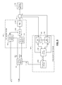
- a radio frequency (RF) generator module 104 receives alternating current (AC) input power and generates an RF output using the AC input power.
- the RF output is applied to a plasma electrode 108 of a plasma chamber 112 .
- the RF output may be used differently.
- the plasma electrode 108 may be used, for example, in thin film deposition, thin film etching, and other types of systems.
- An output control module 116 receives a power setpoint (P Set) for the RF output that is generated by the RF generator module 104 and that is delivered to the plasma electrode 108 .
- the power setpoint may be provided, for example, via an external interface 120 or another suitable source.
- the external interface 120 may provide the power setpoint to the output control module 116 , for example, based on a diagnostic or user input provided via a universal standard (US) 232 connection, via an Ethernet connection, via a wireless connection, or via a front panel interface.
- USB universal standard
- An RF sensor 124 measures one or more parameters of the RF output and generates an RF signal based on the measured parameter(s).
- the RF sensor 124 may include a voltage-current (VI) sensor, an RF probe, a directional coupler, a gamma sensor, a phase-magnitude sensor, or another suitable type of RF sensor.
- a measurement control module 128 samples the RF signal at a predetermined sampling frequency.
- the measurement control module 128 converts the (analog) samples into corresponding digital values.
- the measurement control module 128 also applies one or more signal processing functions to the digital values to produce processed values.
- the output control module 116 controls magnitude, frequency, and phase of the RF output.
- the output control module 116 may selectively update one or more parameters used to control the RF output at a predetermined updating frequency.
- the predetermined updating frequency is less than the predetermined sampling frequency.
- the measurement control module 128 may sample the RF signal on multiple occasions between consecutive times when the output control module 116 may update one or more parameters used to control the RF output.
- the output control module 116 may selectively update one or more of the parameters, for example, based on the processed values from the measurement control module 128 .
- a delay associated with the sampling frequency of the measurement control module 128 and the signal processing function(s) performed to generate the processed values may cause the processed values to be non-time aligned with the updating.
- the non-alignment in time of the processed values with the updating may cause the output control module 116 to incorrectly adjust one or more of the parameters used to control the RF output.
- FIG. 2 is a graph of power versus time for a system where the processed values are non-aligned in time with the updating performed by the output control module 116 .
- Solid trace 204 tracks a target power of the RF output
- dotted trace 208 tracks the actual power of the RF output.
- the output control module 116 may cause the RF output to overshoot a target based on the non-alignment of the processed values with the updating. While the example of overshoot is provided, other output controllers may undershoot or both under and overshoot a target based on the non-alignment of the processed values.
- the measurement control module 128 therefore provides the processed values to the output control module 116 each time that a transition in the RF output is detected.
- the transition may be an increase or a decrease in the RF output.
- the provision of the processed values is synchronized in time with the transitions in the RF output. Based on these processed values that are time-aligned with the transitions in the RF output and based on the setpoint values that resulted in those processed values, the output control module 116 may more accurately control the RF output.
- the output control module 116 may generate a rail voltage setpoint (Rail Set) and a driver control setpoint (Driver Set) based on the power setpoint. Based on the rail voltage setpoint, a power supply module 304 generates a rail voltage from the AC input power. The power supply module 304 applies the rail voltage to a driver 308 .
- Rail Set rail voltage setpoint
- Driver Set driver control setpoint
- a driver control module 312 drives the driver 308 based on the driver control setpoint.
- the driver control setpoint may indicate a target duty cycle (i.e., a percentage of ON time for each predetermined period).
- the driver control module 312 may generate a pulse width modulation (PWM) signal having the target duty cycle and apply the PWM signal to the driver 308 .
- PWM pulse width modulation
- the driver 308 generates an RF output based on the PWM signal and the rail voltage.
- a filter 316 may be implemented to filter the output of the driver 308 before the RF output is applied to the plasma electrode 108 .
- First and second analog to digital converter (ADC) modules 330 and 334 receive first and second parameters (X1 and X2) of the RF output measured by the RF sensor 124 .
- the first and second parameters may be voltage and current or other suitable parameters measured by RF sensors.
- one parameter or more than two parameters may be measured.
- the first and second ADC modules 330 and 334 sample the first and second parameters at a predetermined sampling frequency (Ts ⁇ 1 ) and digitize the samples to produce first and second digital values (D1 and D2).
- a processing module 338 performs one or more signal processing functions on the first and second digital values to produce first and second processed values (P1 and P2).
- the processing module 338 may, for example, apply one or more filters (e.g., a band pass filter) and/or perform one or more other suitable signal processing functions.
- a band pass filter may be applied, for example, to reject out of band measurements from the RF sensor 124 .
- a synchronization module 342 outputs the current processed values to the output control module 116 as synchronized values (S1 and S2) when a level transition in the RF output is detected.
- the processed values may be updated one or more times before a level transition is detected.
- the level transition in the RF output may be an increase or a decrease in one or more parameters of the RF output. While the example of a two-level RF output is provided in the example of FIG. 2 , the output control module 116 may modulate the RF output to three or more different levels in various implementations.
- the synchronization module 342 may detect a level transition, for example, when the first parameter and/or the second parameter measured by the RF sensor 124 increases or decreases. The synchronization module 342 may require that the increase or decrease be greater than a predetermined amount. In various implementations, the synchronization module 342 may detect a transition in the RF output based on another suitable indicator of a transition in the RF output, such as the output of the driver control module 312 , the rail voltage, etc.
- the output control module 116 may selectively adjust the rail voltage setpoint and/or the driver control setpoint based on the synchronized values. Based on these values, the output control module 116 may more accurately control the RF output.
- FIG. 4 is an example graph of power versus time where the provision of the processed values is aligned with level transitions in the RF output.
- Solid trace 404 tracks a target power of the RF output
- dotted trace 408 tracks the actual power of RF output. Relative to the example graph of FIG. 2 , it can be seen that use of the time aligned values may decrease overshoot.
- the coherent pulse generator can improve the repeatability of the pulse front because the measurement and control are synchronized with level transition.
- FIG. 5 another functional block diagram including an example portion of the RF plasma chamber system is presented.
- the first and second ADC modules 330 and 334 sample the first and second parameters at the predetermined sampling frequency (Ts ⁇ 1 ) and digitize the samples to produce first and second digital values (D1 and D2).
- a synchronization module 504 outputs the current digital values as synchronized values (S1 and S2) when a level transition in the RF output is detected.
- the synchronization module 504 may detect the occurrence of a level transition as discussed above.
- a processing module 508 performs one or more signal processing functions on the first and second digital values to produce first and second processed values (P1 and P2).
- the processing module 508 may, for example, apply one or more filters (e.g., a band pass filter) and/or perform one or more other suitable signal processing functions.
- the processing module 508 outputs the processed values to the output control module 116 , and the output control module 116 may selectively adjust the rail voltage setpoint and/or the driver control setpoint based on the processed values.
- a sampling frequency module 604 determines a sample frequency (Ts ⁇ 1 ) based on a period between level transitions in the RF output.
- the sampling frequency module 604 may detect transitions in the RF output, for example, when the first parameter and/or the second parameter measured by the RF sensor 124 increases or decreases.
- the sampling frequency module 604 may require that the increase or decrease be greater than a predetermined amount.
- the sampling frequency module 604 may detect a transition in the RF output based on another suitable indicator of a transition in the RF output, such as the output of the driver control module 312 , the rail voltage, etc.
- First and second ADC modules 608 and 612 receive the first and second parameters (X1 and X2) of the RF output measured by the RF sensor 124 .
- the first and second ADC modules 608 and 612 sample the first and second parameters at the sampling frequency (Ts ⁇ 1 ) set by the sampling frequency module 604 and digitize the samples to produce first and second digital values (D1 and D2).
- the sampling frequency module 604 sets the sampling frequency based on the period between level transitions
- the first and second ADC modules 608 and 612 may produce the digital values approximately simultaneously with each level transition.
- a processing module 616 performs one or more signal processing functions on the first and second digital values to produce first and second processed values (P1 and P2).
- the processing module 616 may, for example, apply one or more filters (e.g., a band pass filter) and/or perform one or more other suitable signal processing functions.
- the processing module 616 outputs the processed values to the output control module 116 , and the output control module 116 may selectively adjust the rail voltage setpoint and/or the driver control setpoint based on the processed values.
- a measurement control module that is similar or identical to the example measurement control module 128 of FIG. 3 , 5 , or 6 may be provided for each channel of a multi-channel RF generator.
- the present disclosure is discussed in the context of RF generator systems, the present disclosure is applicable to other types of systems that measure an RF output and that selectively transition the level of the RF output based on the measurements, such as matching systems/networks.
- Control may begin with 704 where the first and second ADC modules 330 and 334 reset and start first and second timers, respectively.
- the first and second ADC modules 330 and 334 reset the first and second timers to a predetermined period corresponding to the predetermined sampling frequency (i.e., 1/the predetermined sampling frequency). While two timers are discussed, one timer may be used in various implementations.
- the first and second ADC modules 330 and 334 determine whether the values of the first and second timers are equal to zero. If 708 is false, the first and second ADC modules 330 and 334 decrement the first and second timers at 712 , and control returns to 708 . If 708 is true, control continues with 716 . While resetting the timers based on the predetermined period, decrementing the timers, and comparing the timers with zero has been discussed, resetting to zero, incrementing, and determining whether the timers are greater than or equal to the predetermined period may be used.
- the first and second ADC modules 330 and 334 sample the first and second parameters measured by the RF sensor 124 and digitize the samples to produce first and second digital values.
- the first and second ADC modules 330 and 334 hold the first and second digital values until a next time that first and second parameters are sampled and digitized. Control returns to 704 after 716 .
- FIG. 8 a flowchart depicting an example method of providing values of the measurements of the RF sensor 124 corresponding to level transitions in the RF output and controlling the RF output based on the values is presented.
- the method may be performed, for example, by the measurement control module 128 of FIG. 3 and may be executed in parallel with the execution of the method of FIG. 7 .
- Control may begin with 804 where the processing module 338 processes the first and second digital values output by the first and second ADC modules 330 and 334 to produce the first and second processed values.
- the synchronization module 342 determines whether a transition in the level of the RF output has occurred. If 808 is false, control may return to 804 . If 808 is true, control may continue with 812 .
- the synchronization module 342 outputs the first and second processed values as the first and second synchronized values.
- the output control module 116 may selectively adjust the rail voltage setpoint and/or the driver control setpoint at 816 based on the first and/or second synchronized values. Control may then return to 804 .
- FIG. 9 a flowchart depicting another example method of providing values of the measurements of the RF sensor 124 corresponding to level transitions in the RF output and controlling the RF output based on the values is presented.
- the method may be performed, for example, by the measurement control module 128 of FIG. 5 and may be executed in parallel with the execution of the method of FIG. 7 .
- Control may begin with 904 where the synchronization module 504 determines whether a transition in the level of the RF output has occurred. If 904 is false, control may remain at 904 . If 904 is true, control may continue with 908 .
- the synchronization module 504 outputs the first and second digital values as the first and second synchronized values.
- the processing module 508 processes the first and second synchronized values at 912 to produce the first and second processed values.
- the output control module 116 may selectively adjust the rail voltage setpoint and/or the driver control setpoint at 816 based on the first and/or second processed values. Control may then return to 904 .
- FIG. 10 a flowchart depicting another example method of providing values of the measurements of the RF sensor 124 corresponding to level transitions in the RF output and controlling the RF output based on the values is presented The method may be performed, for example, by the measurement control module 128 of FIG. 6 .
- Control may begin with 1004 where the first and second ADC modules 608 and 612 receive the sampling frequency.
- the sampling frequency module 604 determines the period between level transitions in the RF output and determines the sampling frequency based on the period between level transitions.
- the sampling frequency module 604 may determine and/or update the sampling frequency in parallel with the execution of the method of FIG. 10 .
- the first and second ADC modules 608 and 612 reset and start first and second timers, respectively.
- the first and second ADC modules 608 and 612 reset the first and second timers to a period corresponding to the sampling frequency (i.e., 1/the sampling frequency). While two timers are discussed, one timer may be used in various implementations.
- the first and second ADC modules 608 and 612 determine whether the values of the first and second timers are equal to zero. If 1012 is false, the first and second ADC modules 608 and 612 decrement the first and second timers at 1016 , and control returns to 1012 . If 1012 is true, control continues with 1020 . While resetting the timers based on the period, decrementing the timers, and comparing the timers with zero has been discussed, resetting to zero, incrementing, and determining whether the timers are greater than or equal to the period may be used.
- the first and second ADC modules 608 and 612 sample the first and second parameters measured by the RF sensor 124 and digitize the samples to produce first and second digital values.
- the processing module 616 processes the first and second digital values to produce the first and second processed values.
- the output control module 116 may selectively adjust the rail voltage setpoint and/or the driver control setpoint at 1028 based on the first and/or second processed values. Control may then return to 1004 .
- module may be replaced with the term circuit.
- the term module may refer to, be part of, or include an Application Specific Integrated Circuit (ASIC); a digital, analog, or mixed analog/digital discrete circuit; a digital, analog, or mixed analog/digital integrated circuit; a combinational logic circuit; a field programmable gate array (FPGA); a processor (shared, dedicated, or group) that executes code; memory (shared, dedicated, or group) that stores code executed by a processor; other suitable hardware components that provide the described functionality; or a combination of some or all of the above, such as in a system-on-chip.
- ASIC Application Specific Integrated Circuit
- FPGA field programmable gate array
- code may include software, firmware, and/or microcode, and may refer to programs, routines, functions, classes, and/or objects.
- shared processor encompasses a single processor that executes some or all code from multiple modules.
- group processor encompasses a processor that, in combination with additional processors, executes some or all code from one or more modules.
- shared memory encompasses a single memory that stores some or all code from multiple modules.
- group memory encompasses a memory that, in combination with additional memories, stores some or all code from one or more modules.
- the term memory may be a subset of the term computer-readable medium.
- Non-limiting examples of a non-transitory tangible computer readable medium include nonvolatile memory, volatile memory, magnetic storage, and optical storage.
- the apparatuses and methods described in this application may be partially or fully implemented by one or more computer programs executed by one or more processors.
- the computer programs include processor-executable instructions that are stored on at least one non-transitory tangible computer readable medium.
- the computer programs may also include and/or rely on stored data.
Priority Applications (8)
| Application Number | Priority Date | Filing Date | Title |
|---|---|---|---|
| US13/761,955 US9136093B2 (en) | 2013-02-07 | 2013-02-07 | Synchronization of RF pulsing with RF metrology, processing, and control |
| EP13874577.3A EP2954759B1 (en) | 2013-02-07 | 2013-11-21 | Synchronization of rf pulsing with rf metrology, processing, and control |
| JP2015556935A JP6204504B2 (ja) | 2013-02-07 | 2013-11-21 | Rf計測学によるrfパルスの同期、処理、および制御 |
| KR1020157023383A KR101753694B1 (ko) | 2013-02-07 | 2013-11-21 | Rf 측정, 처리 및 제어를 동반하는 rf 펄스 신호의 동기화 |
| PCT/US2013/071244 WO2014123599A1 (en) | 2013-02-07 | 2013-11-21 | Synchronization of rf pulsing with rf metrology, processing, and control |
| EP20166376.2A EP3723458A1 (en) | 2013-02-07 | 2013-11-21 | Synchronization of rf pulsing with rf metrology, processing and control |
| CN201380072406.4A CN104969666B (zh) | 2013-02-07 | 2013-11-21 | Rf脉冲发生与rf计量、处理和控制的同步 |
| TW103100722A TWI563883B (en) | 2013-02-07 | 2014-01-08 | Synchronization of rf pulsing with rf metrology, processing, and control |
Applications Claiming Priority (1)
| Application Number | Priority Date | Filing Date | Title |
|---|---|---|---|
| US13/761,955 US9136093B2 (en) | 2013-02-07 | 2013-02-07 | Synchronization of RF pulsing with RF metrology, processing, and control |
Publications (2)
| Publication Number | Publication Date |
|---|---|
| US20140218076A1 US20140218076A1 (en) | 2014-08-07 |
| US9136093B2 true US9136093B2 (en) | 2015-09-15 |
Family
ID=51258754
Family Applications (1)
| Application Number | Title | Priority Date | Filing Date |
|---|---|---|---|
| US13/761,955 Active US9136093B2 (en) | 2013-02-07 | 2013-02-07 | Synchronization of RF pulsing with RF metrology, processing, and control |
Country Status (7)
| Country | Link |
|---|---|
| US (1) | US9136093B2 (ko) |
| EP (2) | EP2954759B1 (ko) |
| JP (1) | JP6204504B2 (ko) |
| KR (1) | KR101753694B1 (ko) |
| CN (1) | CN104969666B (ko) |
| TW (1) | TWI563883B (ko) |
| WO (1) | WO2014123599A1 (ko) |
Cited By (2)
| Publication number | Priority date | Publication date | Assignee | Title |
|---|---|---|---|---|
| US20160163514A1 (en) * | 2014-12-04 | 2016-06-09 | Mks Instruments, Inc. | Adaptive Periodic Waveform Controller |
| US11706723B2 (en) | 2021-06-09 | 2023-07-18 | XP Power Limited | Radio frequency generator with automatic level control |
Families Citing this family (33)
| Publication number | Priority date | Publication date | Assignee | Title |
|---|---|---|---|---|
| US9496122B1 (en) | 2014-01-10 | 2016-11-15 | Reno Technologies, Inc. | Electronically variable capacitor and RF matching network incorporating same |
| US9196459B2 (en) | 2014-01-10 | 2015-11-24 | Reno Technologies, Inc. | RF impedance matching network |
| US10455729B2 (en) | 2014-01-10 | 2019-10-22 | Reno Technologies, Inc. | Enclosure cooling system |
| US10431428B2 (en) | 2014-01-10 | 2019-10-01 | Reno Technologies, Inc. | System for providing variable capacitance |
| US9844127B2 (en) | 2014-01-10 | 2017-12-12 | Reno Technologies, Inc. | High voltage switching circuit |
| US9697991B2 (en) | 2014-01-10 | 2017-07-04 | Reno Technologies, Inc. | RF impedance matching network |
| US9755641B1 (en) | 2014-01-10 | 2017-09-05 | Reno Technologies, Inc. | High speed high voltage switching circuit |
| JP6309398B2 (ja) * | 2014-08-29 | 2018-04-11 | 株式会社ダイヘン | 高周波電源 |
| US9729122B2 (en) | 2015-02-18 | 2017-08-08 | Reno Technologies, Inc. | Switching circuit |
| US10340879B2 (en) | 2015-02-18 | 2019-07-02 | Reno Technologies, Inc. | Switching circuit |
| US11017983B2 (en) | 2015-02-18 | 2021-05-25 | Reno Technologies, Inc. | RF power amplifier |
| US9306533B1 (en) | 2015-02-20 | 2016-04-05 | Reno Technologies, Inc. | RF impedance matching network |
| US9525412B2 (en) | 2015-02-18 | 2016-12-20 | Reno Technologies, Inc. | Switching circuit |
| US10984986B2 (en) | 2015-06-29 | 2021-04-20 | Reno Technologies, Inc. | Impedance matching network and method |
| US11342160B2 (en) | 2015-06-29 | 2022-05-24 | Reno Technologies, Inc. | Filter for impedance matching |
| US11081316B2 (en) | 2015-06-29 | 2021-08-03 | Reno Technologies, Inc. | Impedance matching network and method |
| US11335540B2 (en) | 2015-06-29 | 2022-05-17 | Reno Technologies, Inc. | Impedance matching network and method |
| US11150283B2 (en) | 2015-06-29 | 2021-10-19 | Reno Technologies, Inc. | Amplitude and phase detection circuit |
| US11342161B2 (en) | 2015-06-29 | 2022-05-24 | Reno Technologies, Inc. | Switching circuit with voltage bias |
| US10692699B2 (en) | 2015-06-29 | 2020-06-23 | Reno Technologies, Inc. | Impedance matching with restricted capacitor switching |
| US10727029B2 (en) | 2017-07-10 | 2020-07-28 | Reno Technologies, Inc | Impedance matching using independent capacitance and frequency control |
| US11114280B2 (en) | 2017-07-10 | 2021-09-07 | Reno Technologies, Inc. | Impedance matching with multi-level power setpoint |
| US11289307B2 (en) | 2017-07-10 | 2022-03-29 | Reno Technologies, Inc. | Impedance matching network and method |
| US10714314B1 (en) | 2017-07-10 | 2020-07-14 | Reno Technologies, Inc. | Impedance matching network and method |
| US10483090B2 (en) | 2017-07-10 | 2019-11-19 | Reno Technologies, Inc. | Restricted capacitor switching |
| US11393659B2 (en) | 2017-07-10 | 2022-07-19 | Reno Technologies, Inc. | Impedance matching network and method |
| US11398370B2 (en) | 2017-07-10 | 2022-07-26 | Reno Technologies, Inc. | Semiconductor manufacturing using artificial intelligence |
| US11476091B2 (en) | 2017-07-10 | 2022-10-18 | Reno Technologies, Inc. | Impedance matching network for diagnosing plasma chamber |
| US11315758B2 (en) | 2017-07-10 | 2022-04-26 | Reno Technologies, Inc. | Impedance matching using electronically variable capacitance and frequency considerations |
| US11101110B2 (en) | 2017-07-10 | 2021-08-24 | Reno Technologies, Inc. | Impedance matching network and method |
| US11521833B2 (en) | 2017-07-10 | 2022-12-06 | Reno Technologies, Inc. | Combined RF generator and RF solid-state matching network |
| CN109219225A (zh) * | 2018-10-18 | 2019-01-15 | 哈尔滨工业大学 | 诊断交流放电等离子体参数的数据采集方法 |
| US11521831B2 (en) | 2019-05-21 | 2022-12-06 | Reno Technologies, Inc. | Impedance matching network and method with reduced memory requirements |
Citations (6)
| Publication number | Priority date | Publication date | Assignee | Title |
|---|---|---|---|---|
| EP0677221A1 (en) | 1992-12-30 | 1995-10-18 | Nokia Telecommunications Oy | Method and arrangement for tuning a combiner filter |
| US6252354B1 (en) | 1996-11-04 | 2001-06-26 | Applied Materials, Inc. | RF tuning method for an RF plasma reactor using frequency servoing and power, voltage, current or DI/DT control |
| US6459067B1 (en) | 2001-04-06 | 2002-10-01 | Eni Technology, Inc. | Pulsing intelligent RF modulation controller |
| US20060232471A1 (en) * | 2005-04-18 | 2006-10-19 | Mks Instruments, Inc. | Phase and frequency control of a radio frequency generator from an external source |
| US20080085693A1 (en) * | 2006-08-09 | 2008-04-10 | Harms Brian K | Reference signal generation for multiple communication systems |
| US7839223B2 (en) | 2008-03-23 | 2010-11-23 | Advanced Energy Industries, Inc. | Method and apparatus for advanced frequency tuning |
Family Cites Families (8)
| Publication number | Priority date | Publication date | Assignee | Title |
|---|---|---|---|---|
| JPH02150766U (ko) * | 1989-05-25 | 1990-12-27 | ||
| US6841124B2 (en) * | 2000-10-02 | 2005-01-11 | Ethicon, Inc. | Sterilization system with a plasma generator controlled by a digital signal processor |
| TWI339546B (en) * | 2004-04-30 | 2011-03-21 | Applied Materials Inc | Plasma chamber and method of processing substrate in the same |
| US20060109061A1 (en) | 2004-11-22 | 2006-05-25 | Masterwave, Inc. | System and method for narrow bandwidth amplitude modulation |
| US7477711B2 (en) * | 2005-05-19 | 2009-01-13 | Mks Instruments, Inc. | Synchronous undersampling for high-frequency voltage and current measurements |
| KR101022868B1 (ko) * | 2009-08-17 | 2011-03-16 | 엘에스산전 주식회사 | Rf노이즈 신호를 상쇄하는 rfid 안테나 시스템 및 이를 이용한 rfid 안테나 시스템의 제어방법 |
| US8314561B2 (en) * | 2010-04-02 | 2012-11-20 | Mks Instruments, Inc. | Multi-channel radio frequency generator |
| JP5606365B2 (ja) * | 2011-03-10 | 2014-10-15 | 株式会社東芝 | 受信装置、復調装置、復調方法及び復調プログラム |
-
2013
- 2013-02-07 US US13/761,955 patent/US9136093B2/en active Active
- 2013-11-21 KR KR1020157023383A patent/KR101753694B1/ko active IP Right Grant
- 2013-11-21 WO PCT/US2013/071244 patent/WO2014123599A1/en active Application Filing
- 2013-11-21 EP EP13874577.3A patent/EP2954759B1/en active Active
- 2013-11-21 JP JP2015556935A patent/JP6204504B2/ja active Active
- 2013-11-21 EP EP20166376.2A patent/EP3723458A1/en active Pending
- 2013-11-21 CN CN201380072406.4A patent/CN104969666B/zh active Active
-
2014
- 2014-01-08 TW TW103100722A patent/TWI563883B/zh active
Patent Citations (6)
| Publication number | Priority date | Publication date | Assignee | Title |
|---|---|---|---|---|
| EP0677221A1 (en) | 1992-12-30 | 1995-10-18 | Nokia Telecommunications Oy | Method and arrangement for tuning a combiner filter |
| US6252354B1 (en) | 1996-11-04 | 2001-06-26 | Applied Materials, Inc. | RF tuning method for an RF plasma reactor using frequency servoing and power, voltage, current or DI/DT control |
| US6459067B1 (en) | 2001-04-06 | 2002-10-01 | Eni Technology, Inc. | Pulsing intelligent RF modulation controller |
| US20060232471A1 (en) * | 2005-04-18 | 2006-10-19 | Mks Instruments, Inc. | Phase and frequency control of a radio frequency generator from an external source |
| US20080085693A1 (en) * | 2006-08-09 | 2008-04-10 | Harms Brian K | Reference signal generation for multiple communication systems |
| US7839223B2 (en) | 2008-03-23 | 2010-11-23 | Advanced Energy Industries, Inc. | Method and apparatus for advanced frequency tuning |
Cited By (8)
| Publication number | Priority date | Publication date | Assignee | Title |
|---|---|---|---|---|
| US20160163514A1 (en) * | 2014-12-04 | 2016-06-09 | Mks Instruments, Inc. | Adaptive Periodic Waveform Controller |
| US10049857B2 (en) * | 2014-12-04 | 2018-08-14 | Mks Instruments, Inc. | Adaptive periodic waveform controller |
| US20180294141A1 (en) * | 2014-12-04 | 2018-10-11 | Mks Instruments, Inc. | Adaptive Periodic Waveform Controller |
| US10217609B2 (en) * | 2014-12-04 | 2019-02-26 | Mks Instruments, Inc. | Adaptive periodic waveform controller |
| US20190214231A1 (en) * | 2014-12-04 | 2019-07-11 | Mks Instruments, Inc. | Adaptive Periodic Waveform Controller |
| US10727027B2 (en) * | 2014-12-04 | 2020-07-28 | Mks Instruments, Inc. | Adaptive periodic waveform controller |
| US11367592B2 (en) * | 2014-12-04 | 2022-06-21 | Mks Instruments, Inc. | Adaptive periodic waveform controller |
| US11706723B2 (en) | 2021-06-09 | 2023-07-18 | XP Power Limited | Radio frequency generator with automatic level control |
Also Published As
| Publication number | Publication date |
|---|---|
| CN104969666B (zh) | 2018-06-19 |
| TWI563883B (en) | 2016-12-21 |
| EP2954759B1 (en) | 2020-05-06 |
| JP2016513340A (ja) | 2016-05-12 |
| EP2954759A1 (en) | 2015-12-16 |
| CN104969666A (zh) | 2015-10-07 |
| JP6204504B2 (ja) | 2017-09-27 |
| TW201433218A (zh) | 2014-08-16 |
| EP2954759A4 (en) | 2016-08-10 |
| KR101753694B1 (ko) | 2017-07-04 |
| KR20150116873A (ko) | 2015-10-16 |
| EP3723458A1 (en) | 2020-10-14 |
| US20140218076A1 (en) | 2014-08-07 |
| WO2014123599A1 (en) | 2014-08-14 |
Similar Documents
| Publication | Publication Date | Title |
|---|---|---|
| US9136093B2 (en) | Synchronization of RF pulsing with RF metrology, processing, and control | |
| US8952765B2 (en) | System and methods of bimodal automatic power and frequency tuning of RF generators | |
| US9368329B2 (en) | Methods and apparatus for synchronizing RF pulses in a plasma processing system | |
| CN107466419B (zh) | 对等离子体过程的供电期间出现的电弧进行检测的方法、等离子体电源的控制单元、以及等离子体电源 | |
| US9837809B2 (en) | Arc detection apparatus, arc detecting method, and power system | |
| KR101512107B1 (ko) | 전기전도도 측정장치 및 이를 이용한 전기전도도의 측정방법 | |
| US20150061391A1 (en) | Electronic control device | |
| US8373487B1 (en) | True RMS power measurement | |
| CN109188889B (zh) | 一种原子钟1pps时间同步方法和系统 | |
| KR102004842B1 (ko) | 프린트 기판의 절연 검사 장치 및 절연 검사 방법 | |
| WO2017161870A1 (zh) | 一种频率调节的方法及装置 | |
| EP3255445B1 (en) | Magneto-impedance (mi) magnetic sensor | |
| CN109313460B (zh) | 交流电力调整器 | |
| US11719663B2 (en) | Measuring apparatus | |
| KR101383264B1 (ko) | 이온 트랩 질량분석기 | |
| JP6312062B2 (ja) | 電力計測装置及び電力計測方法 | |
| CN105763194A (zh) | 处理器芯片的采样电压调节方法、装置和处理器芯片 | |
| KR20180084437A (ko) | 멀티 코일 측정 방법 및 멀티 코일 측정 장치 | |
| KR20160139696A (ko) | 전압 변환 장치 | |
| JP2013034119A (ja) | 位相比較装置 | |
| TW201619616A (zh) | 測試系統及其相位檢測裝置及方法 |
Legal Events
| Date | Code | Title | Description |
|---|---|---|---|
| AS | Assignment |
Owner name: MKS INSTRUMENTS, INC., MASSACHUSETTS Free format text: ASSIGNMENT OF ASSIGNORS INTEREST;ASSIGNORS:COUMOU, DAVID J.;FISK, LARRY J.;RADOMSKI, AARON T.;AND OTHERS;SIGNING DATES FROM 20130226 TO 20130228;REEL/FRAME:030297/0912 |
|
| STCF | Information on status: patent grant |
Free format text: PATENTED CASE |
|
| AS | Assignment |
Owner name: DEUTSCHE BANK AG NEW YORK BRANCH, NEW YORK Free format text: SECURITY AGREEMENT;ASSIGNORS:MKS INSTRUMENTS, INC.;NEWPORT CORPORATION;REEL/FRAME:038663/0265 Effective date: 20160429 Owner name: BARCLAYS BANK PLC, NEW YORK Free format text: SECURITY AGREEMENT;ASSIGNORS:MKS INSTRUMENTS, INC.;NEWPORT CORPORATION;REEL/FRAME:038663/0139 Effective date: 20160429 |
|
| AS | Assignment |
Owner name: BARCLAYS BANK PLC, AS COLLATERAL AGENT, NEW YORK Free format text: PATENT SECURITY AGREEMENT (ABL);ASSIGNORS:ELECTRO SCIENTIFIC INDUSTRIES, INC.;MKS INSTRUMENTS, INC.;NEWPORT CORPORATION;REEL/FRAME:048211/0312 Effective date: 20190201 Owner name: NEWPORT CORPORATION, CALIFORNIA Free format text: RELEASE BY SECURED PARTY;ASSIGNOR:DEUTSCHE BANK AG NEW YORK BRANCH;REEL/FRAME:048226/0095 Effective date: 20190201 Owner name: MKS INSTRUMENTS, INC., MASSACHUSETTS Free format text: RELEASE BY SECURED PARTY;ASSIGNOR:DEUTSCHE BANK AG NEW YORK BRANCH;REEL/FRAME:048226/0095 Effective date: 20190201 |
|
| MAFP | Maintenance fee payment |
Free format text: PAYMENT OF MAINTENANCE FEE, 4TH YEAR, LARGE ENTITY (ORIGINAL EVENT CODE: M1551); ENTITY STATUS OF PATENT OWNER: LARGE ENTITY Year of fee payment: 4 |
|
| AS | Assignment |
Owner name: BARCLAYS BANK PLC, AS COLLATERAL AGENT, NEW YORK Free format text: CORRECTIVE ASSIGNMENT TO CORRECT THE REMOVE U.S. PATENT NO.7,919,646 PREVIOUSLY RECORDED ON REEL 048211 FRAME 0312. ASSIGNOR(S) HEREBY CONFIRMS THE PATENT SECURITY AGREEMENT (ABL);ASSIGNORS:ELECTRO SCIENTIFIC INDUSTRIES, INC.;MKS INSTRUMENTS, INC.;NEWPORT CORPORATION;REEL/FRAME:055668/0687 Effective date: 20190201 |
|
| AS | Assignment |
Owner name: JPMORGAN CHASE BANK, N.A., AS COLLATERAL AGENT, ILLINOIS Free format text: SECURITY INTEREST;ASSIGNORS:MKS INSTRUMENTS, INC.;NEWPORT CORPORATION;ELECTRO SCIENTIFIC INDUSTRIES, INC.;REEL/FRAME:061572/0069 Effective date: 20220817 |
|
| AS | Assignment |
Owner name: ELECTRO SCIENTIFIC INDUSTRIES, INC., OREGON Free format text: RELEASE BY SECURED PARTY;ASSIGNOR:BARCLAYS BANK PLC;REEL/FRAME:063009/0001 Effective date: 20220817 Owner name: NEWPORT CORPORATION, MASSACHUSETTS Free format text: RELEASE BY SECURED PARTY;ASSIGNOR:BARCLAYS BANK PLC;REEL/FRAME:063009/0001 Effective date: 20220817 Owner name: MKS INSTRUMENTS, INC., MASSACHUSETTS Free format text: RELEASE BY SECURED PARTY;ASSIGNOR:BARCLAYS BANK PLC;REEL/FRAME:063009/0001 Effective date: 20220817 Owner name: ELECTRO SCIENTIFIC INDUSTRIES, INC., OREGON Free format text: RELEASE BY SECURED PARTY;ASSIGNOR:BARCLAYS BANK PLC;REEL/FRAME:062739/0001 Effective date: 20220817 Owner name: NEWPORT CORPORATION, MASSACHUSETTS Free format text: RELEASE BY SECURED PARTY;ASSIGNOR:BARCLAYS BANK PLC;REEL/FRAME:062739/0001 Effective date: 20220817 Owner name: MKS INSTRUMENTS, INC., MASSACHUSETTS Free format text: RELEASE BY SECURED PARTY;ASSIGNOR:BARCLAYS BANK PLC;REEL/FRAME:062739/0001 Effective date: 20220817 |
|
| MAFP | Maintenance fee payment |
Free format text: PAYMENT OF MAINTENANCE FEE, 8TH YEAR, LARGE ENTITY (ORIGINAL EVENT CODE: M1552); ENTITY STATUS OF PATENT OWNER: LARGE ENTITY Year of fee payment: 8 |