US9036106B2 - Liquid crystal display device in which array substrate includes black matrix and method of manufacturing the same - Google Patents

Liquid crystal display device in which array substrate includes black matrix and method of manufacturing the same Download PDF

Info

Publication number
US9036106B2
US9036106B2 US13/403,297 US201213403297A US9036106B2 US 9036106 B2 US9036106 B2 US 9036106B2 US 201213403297 A US201213403297 A US 201213403297A US 9036106 B2 US9036106 B2 US 9036106B2
Authority
US
United States
Prior art keywords
substrate
layer
black matrix
color filter
liquid crystal
Prior art date
Legal status (The legal status is an assumption and is not a legal conclusion. Google has not performed a legal analysis and makes no representation as to the accuracy of the status listed.)
Active, expires
Application number
US13/403,297
Other versions
US20120249936A1 (en
Inventor
Yubao ZI
Jaeyun Jung
Shikai WANG
Daiwu WU
Zhi HOU
Current Assignee (The listed assignees may be inaccurate. Google has not performed a legal analysis and makes no representation or warranty as to the accuracy of the list.)
BOE Technology Group Co Ltd
Hefei BOE Optoelectronics Technology Co Ltd
Original Assignee
BOE Technology Group Co Ltd
Hefei BOE Optoelectronics Technology Co Ltd
Priority date (The priority date is an assumption and is not a legal conclusion. Google has not performed a legal analysis and makes no representation as to the accuracy of the date listed.)
Filing date
Publication date
Application filed by BOE Technology Group Co Ltd, Hefei BOE Optoelectronics Technology Co Ltd filed Critical BOE Technology Group Co Ltd
Assigned to HEFEI BOE OPTOELECTRONICS TECHNOLOGY CO., LTD., BOE TECHNOLOGY GROUP CO., LTD. reassignment HEFEI BOE OPTOELECTRONICS TECHNOLOGY CO., LTD. ASSIGNMENT OF ASSIGNORS INTEREST (SEE DOCUMENT FOR DETAILS). Assignors: HOU, Zhi, WU, DAIWU, ZI, YUBAO, JUNG, JAEYUN, WANG, SHIKAI
Publication of US20120249936A1 publication Critical patent/US20120249936A1/en
Application granted granted Critical
Publication of US9036106B2 publication Critical patent/US9036106B2/en
Active legal-status Critical Current
Adjusted expiration legal-status Critical

Links

Images

Classifications

    • H01L27/1288
    • HELECTRICITY
    • H10SEMICONDUCTOR DEVICES; ELECTRIC SOLID-STATE DEVICES NOT OTHERWISE PROVIDED FOR
    • H10DINORGANIC ELECTRIC SEMICONDUCTOR DEVICES
    • H10D86/00Integrated devices formed in or on insulating or conducting substrates, e.g. formed in silicon-on-insulator [SOI] substrates or on stainless steel or glass substrates
    • H10D86/01Manufacture or treatment
    • H10D86/021Manufacture or treatment of multiple TFTs
    • H10D86/0231Manufacture or treatment of multiple TFTs using masks, e.g. half-tone masks
    • GPHYSICS
    • G02OPTICS
    • G02FOPTICAL DEVICES OR ARRANGEMENTS FOR THE CONTROL OF LIGHT BY MODIFICATION OF THE OPTICAL PROPERTIES OF THE MEDIA OF THE ELEMENTS INVOLVED THEREIN; NON-LINEAR OPTICS; FREQUENCY-CHANGING OF LIGHT; OPTICAL LOGIC ELEMENTS; OPTICAL ANALOGUE/DIGITAL CONVERTERS
    • G02F1/00Devices or arrangements for the control of the intensity, colour, phase, polarisation or direction of light arriving from an independent light source, e.g. switching, gating or modulating; Non-linear optics
    • G02F1/01Devices or arrangements for the control of the intensity, colour, phase, polarisation or direction of light arriving from an independent light source, e.g. switching, gating or modulating; Non-linear optics for the control of the intensity, phase, polarisation or colour 
    • G02F1/13Devices or arrangements for the control of the intensity, colour, phase, polarisation or direction of light arriving from an independent light source, e.g. switching, gating or modulating; Non-linear optics for the control of the intensity, phase, polarisation or colour  based on liquid crystals, e.g. single liquid crystal display cells
    • G02F1/133Constructional arrangements; Operation of liquid crystal cells; Circuit arrangements
    • G02F1/136Liquid crystal cells structurally associated with a semi-conducting layer or substrate, e.g. cells forming part of an integrated circuit
    • G02F1/1362Active matrix addressed cells
    • G02F1/136209Light shielding layers, e.g. black matrix, incorporated in the active matrix substrate, e.g. structurally associated with the switching element
    • H01L29/78633
    • HELECTRICITY
    • H10SEMICONDUCTOR DEVICES; ELECTRIC SOLID-STATE DEVICES NOT OTHERWISE PROVIDED FOR
    • H10DINORGANIC ELECTRIC SEMICONDUCTOR DEVICES
    • H10D30/00Field-effect transistors [FET]
    • H10D30/60Insulated-gate field-effect transistors [IGFET]
    • H10D30/67Thin-film transistors [TFT]
    • H10D30/6704Thin-film transistors [TFT] having supplementary regions or layers in the thin films or in the insulated bulk substrates for controlling properties of the device
    • H10D30/6723Thin-film transistors [TFT] having supplementary regions or layers in the thin films or in the insulated bulk substrates for controlling properties of the device having light shields

Definitions

  • the present invention relates to a liquid crystal display and a method of manufacturing the same.
  • Thin Film Transistor (TFT)-Liquid Crystal Display comprises an array substrate (TFT substrate), a color filter substrate (CF substrate) and a liquid crystal layer filled between them.
  • the array substrate comprises a first substrate and the color filter substrate comprises a second substrate.
  • the first and second substrate is typically made of glass.
  • FIG. 1 shows a schematic structure of a conventional TFT-LCD.
  • the TFT substrate comprises a bottom gate TFT device 13 in which a gate electrode is formed on a bottom side.
  • the bottom gate TFT device 13 comprises a gate electrode 6 on a first substrate 11 , a gate insulating layer 5 a on the gate electrode 6 , an active layer 2 of a-Si (amorphous silicon) on the gate insulating layer 5 a , and a source electrode (S) 41 /drain electrode 42 (D) on the active layer 2 .
  • S source electrode
  • an ohmic contact layer 3 of N + a-Si with good conductivity may be formed between the S/D layer and the active layer so as to form a good ohmic contact with the S/D layer.
  • the TFT substrate further comprises a passivation protective film 10 and a pixel electrode 7 on the passivation protective layer 10 .
  • the pixel electrode 7 is connected to the S/D layer through via hole 15 formed in the passivation protective layer 19 and is typically formed of transparent conductive materials such as indium tin oxide (ITO).
  • the color filter substrate comprises a black matrix 1 , a color filter layer 9 , and a counter electrode 8 in this order on a second substrate 12 .
  • the counter electrode 8 is typically formed of transparent conductive materials such as indium tin oxide (ITO).
  • ITO indium tin oxide
  • a 5mask process is usually used for manufacturing the TFT substrate.
  • the 5mask process comprises: forming a gate electrode pattern with a gate mask; etching an active layer of a-Si layer and a N+ a-Si layer with an active mask to form an active pattern; forming a SD electrode with SD mask; forming via holes by etching with a passivation protective mask; and forming a ITO pixel electrode layer with an ITO mask.
  • Corresponding exposure processes used in the 5mask process are all conventional exposure method.
  • a-Si of the active layer in TFT device is a photosensitive material and the conducting channel is located in the uppermost layer of the bottom gate TFT device. Therefore, external lights can easily strike on the a-Si serving as the conducting channel during operation of TFT-LCD, resulting in deterioration of off-state property of the TFT device and having an adverse effect on standing property of the TFT-LCD, even causing image flickering and grey level variation in severe conditions.
  • the TFT-LCD generally operates in a normal white mode for TN-type liquid crystal, image contrast would be decreased substantially due to light leakages occurred in non-display regions when displaying a black image.
  • the liquid crystal subjected to a horizontal electric field between signal lines and pixel electrode would suffer a reverse-tilt alignment defect at edges of the pixel, which would decrease the image contrast and sometimes inducing afterimage.
  • the black matrix (BM) on the color filter substrate to overlap (shown as d 1 , d 2 in FIG. 1 ) substantially an area where the pixel electrode 7 is formed on the TFT substrate, so as to ensure no light leakage.
  • BM black matrix
  • the embodiment of the invention provides a liquid crystal display and a method of manufacturing the same.
  • the liquid crystal display of the embodiment of the invention comprises an array substrate, a color filter substrate and a liquid crystal layer formed between the array substrate and the color filter substrate.
  • the array substrate comprises a first substrate; a black matrix formed on the first substrate; and a thin film transistor (TFT) device formed on the black matrix.
  • the TFT device is a top gate TFT device having a gate electrode formed on a side of the TFT device facing away the black matrix.
  • the color filter substrate comprises a second substrate; and a color filter layer formed on the second substrate.
  • the TFT device comprises: an active layer formed on the black matrix; a source electrode and a drain electrode formed on a part of the active layer; an insulating layer formed above the active layer and covering the source electrode and the drain electrode; the gate electrode formed on the insulating layer between the source electrode and the drain electrode.
  • An area occupied by the TFT device on the first substrate is contained within an area occupied by the black matrix on the first substrate.
  • the TFT device and the black matrix occupy the same area on the first substrate.
  • the array substrate further comprises a pixel electrode formed on the insulating layer and connected with the source electrode through via holes in the insulating layer.
  • the pixel electrode is formed of indium tin oxide (ITO).
  • the color filter substrate further comprises a counter electrode formed on the color filter layer.
  • the counter electrode is formed from indium tin oxide (ITO).
  • ITO indium tin oxide
  • the TFT device further comprises an ohmic contact layer formed between the source electrode and the active layer and/or between the drain electrode and the active layer.
  • the first substrate and the second substrate are formed of glass.
  • a method of manufacturing a liquid crystal display in the embodiment of the invention comprises steps of preparing an array substrate, preparing a color filter substrate and assembling the array substrate and the color filter substrate and injecting liquid crystal between the array substrate and the color filter substrate.
  • the step of preparing the array substrate comprises steps of: providing a first substrate; forming a black matrix on the first substrate and forming a thin film transistor (TFT) device on the black matrix.
  • the TFT device is a top gate TFT device having a gate electrode formed on a side of the TFT device facing away the black matrix.
  • the step of preparing the color filter substrate comprises steps of: providing a second substrate; and forming a color filter layer on the second substrate.
  • the step of forming the black matrix and the TFT device on the first substrate comprises: forming a stack layer including a black matrix layer, an active layer and an electrode layer in this order on the first substrate; forming a photoresist layer on the stack layer; patterning the photoresist layer using a half tone mask by a lithography and etching, so as to remove the photoresist layer outside an area where the black matrix is formed, and the patterned photoresist layer is formed with a first thickness in a first area where the gate electrode of the TFT device is formed and a second thickness in a second area outside the first area, wherein the first thickness is less than the second thickness; etching off the stack layer outside the black matrix area using the patterned photoresist layer so as to pattern the stack layer; removing the patterned photoresist layer by the first thickness, and forming separate source electrode and drain electrode using remained photoresist layer; removing the remained photoresist layer by an ashing process, and depositing
  • the step of preparing the array substrate further comprises forming a pixel electrode which is formed on the insulating layer and connected with the source electrode through via holes in the insulating layer.
  • the step of forming the black matrix and the TFT device on the first substrate further comprises forming an ohmic contact layer between the source electrode and the active layer and/or between the drain electrode and the active layer.
  • the black matrix is formed directly on the array substrate, therefore a top gate TFT device can be formed on the array substrate with the gate electrode on a side of the TFT device facing away the black matrix e.
  • Such structure can further improve the aperture ratio of TFT-LCD, and simplify the manufacturing process and reduce production cost due to the use of top gate TFT device.
  • FIG. 1 is a schematic view of a conventional TFT-LCD.
  • FIG. 2 is a schematic view of a TFT-LCD according to an embodiment of the invention.
  • FIGS. 3-5 are flow charts showing a method of manufacturing TFT-LCD according to an embodiment of the invention.
  • FIGS. 6-9 are schematic sectional views showing the step of forming a black matrix and a top gate TFT device on a first substrate according to an embodiment of the invention.
  • FIG. 2 is a schematic view of a TFT-LCD according to an embodiment of the invention.
  • the TFT-LCD according to the embodiment of the invention comprises an array substrate 100 , a color filter substrate 200 and a liquid crystal layer (not shown) formed between the array substrate 100 and the color filter substrate 200 .
  • the array substrate 100 comprises a first substrate 11 , a black matrix 1 formed on the first substrate 11 , and a thin film transistor (TFT) device 13 ′ formed on the black matrix 1 .
  • the TFT device is a top gate TFT device which has a gate electrode 6 formed on a side facing away from the black matrix 1 .
  • the color filter substrate 200 comprises a second substrate 12 and a color filter layer 9 formed on the second substrate 12 .
  • the color filter layer 9 may include red, green and blue color filters.
  • the color filter substrate 200 further comprises a counter electrode 8 formed on the color filter layer 9 .
  • the counter electrode 8 may be formed of transparent conductive materials such as indium tin oxide (ITO).
  • ITO indium tin oxide
  • the first substrate 11 and the second substrate 12 may be formed of glass, for example.
  • the top gate TFT device 13 ′ comprises: an active layer 2 formed on the black matrix 1 ; an ohmic contact layer 3 optionally formed on the active layer 2 ; a source electrode 41 and a drain electrode 42 formed on a part of the ohmic contact layer 3 ; an insulating layer 5 formed above the active layer 2 and covering the source electrode 41 and the drain electrode 42 ; and the gate electrode 6 formed on the insulating layer 5 between the source electrode 41 and the drain electrode 42 .
  • the array substrate 100 further comprises a pixel electrode 7 which is connected to the drain electrode 42 through a via hole 15 in the insulating layer 5 .
  • the pixel electrode 7 may be formed of indium tin oxide (ITO), for example.
  • the area occupied by the top gate TFT device 13 ′ on the first substrate 11 is contained within the area occupied by the black matrix 1 on the first substrate 11 . Further, TFT device 13 ′ and the black matrix 1 may occupy a same area on the first substrate 11 . That is, in the embodiment of the invention, it is sufficient to make the black matrix 1 just cover the TFT device 13 ′ in order to prevent light leakage, without any substantial overlaps (d 1 , d 2 portion shown in FIG. 1 ) between the area occupied by the black matrix 1 and the area occupied by the pixel electrode 7 in the conventional liquid crystal display as shown in FIG. 1 . Therefore, the aperture ratio is improved. Additionally, according to the embodiment of the invention, the overlap (d as shown in FIG.
  • the black matrix is not formed in the color filter substrate, therefore the requirement for process accuracy is less stringent and the process is simpler.
  • FIGS. 3-5 show flow charts of a method of manufacturing liquid crystal display according to an embodiment of the invention.
  • the method comprises steps of preparing an array substrate ( 301 ), preparing a color filter substrate ( 302 ) and assembling the array substrate and the color filter substrate and injecting liquid crystal material between the array substrate and the color filter substrate ( 303 ).
  • the step of preparing the array substrate comprises steps of providing a first substrate ( 401 ); forming a black matrix on the first substrate ( 402 ) and forming a thin film transistor (TFT) device on the black matrix ( 403 ).
  • the TFT device is a top gate TFT device having a gate electrode formed on a side of the TFT device facing away the black matrix.
  • the step of preparing the color filter substrate comprises steps of providing a second substrate ( 501 ) and forming a color filter layer on the second substrate ( 502 ).
  • the steps of forming the black matrix and the TFT device on the first substrate comprises the following steps, as shown in FIGS. 6-9 .
  • a stack layer including a black matrix layer 1 , an active layer 2 , an optional ohmic contact layer 3 and an electrode layer 4 is formed successively in this order on the first substrate 11 .
  • a photoresist layer 21 is formed on the stack layer; and the photoresist layer is patterned using a half tone mask M by photolithography and etching processes so as to remove the photoresist outside an area where the black matrix will be formed.
  • the patterned photoresist layer 22 is formed with a first thickness in an area where the gate electrode 6 will be formed and a second thickness in the area of the black matrix area outside the gate electrode area. The first thickness is less than the second thickness.
  • the stack layer outside the black matrix area is etched off using the patterned photoresist layer 22 so as to pattern the stack layer.
  • the photoresist layer 22 is thinned by the first thickness.
  • the electrode layer 4 is patterned using the remained photoresist layer 23 so as to form a source electrode 41 and a drain electrode 42 separated from each other and expose the channel area between the source electrode 41 and the drain electrode 42 .
  • the remained photoresist layer 23 is removed by an ashing process.
  • an insulating layer 5 may be deposited on the resulting structure, and a gate electrode 6 may be formed on the insulating layer 5 between the source electrode 41 and the drain electrode 42 .
  • via holes may be formed in the insulating layer 5 above the source electrode 41 by a conventional mask process, so as to further form a pixel electrode 7 connected to the source electrode 41 .
  • the black matrix is formed under the top gate TFT device (BM Under TFT), which reduces the overlap area of the black matrix and the pixel electrode.
  • BM Under TFT top gate TFT device
  • the black matrix formed at the bottom blocks lights from a back light source unit disposed below.
  • the gate electrode located on the top of the top gate TFT may also prevent the reflected light from interfering with the active layer (a-Si). Due to these two aspects, the aperture ratio of TFT-LCD is increased.
  • the formation process of the black matrix may be omitted, instead the color filter layer of R, G, B pixels can be formed directly on the glass substrate. Without considerations for the black matrix, the area of the pixel region can be larger, and the requirement for accuracy is lowered, and the process is simpler.
  • the manufacturing process of TFT substrate is simplified to a 4Mask process. This will reduce exposure processes and save the cost.

Landscapes

  • Physics & Mathematics (AREA)
  • Nonlinear Science (AREA)
  • Engineering & Computer Science (AREA)
  • Microelectronics & Electronic Packaging (AREA)
  • Mathematical Physics (AREA)
  • Chemical & Material Sciences (AREA)
  • Crystallography & Structural Chemistry (AREA)
  • General Physics & Mathematics (AREA)
  • Optics & Photonics (AREA)
  • Liquid Crystal (AREA)
  • Thin Film Transistor (AREA)

Abstract

The embodiment of the invention discloses a liquid crystal display and a method of manufacturing the same. The liquid crystal display of the embodiment of the invention comprises an array substrate, a color filter substrate and a liquid crystal layer formed between the array substrate and the color filter substrate. The array substrate comprises a first substrate; a black matrix formed on the first substrate; and a thin film transistor (TFT) device formed on the black matrix. The TFT device is a top gate TFT device having a gate electrode formed on a side of the TFT device facing away the black matrix and an active layer made of a-Si. The color filter substrate comprises a second substrate; and a color filter layer formed on the second substrate. The color filter substrate does not include a black matrix.

Description

BACKGROUND
The present invention relates to a liquid crystal display and a method of manufacturing the same.
Thin Film Transistor (TFT)-Liquid Crystal Display (LCD) comprises an array substrate (TFT substrate), a color filter substrate (CF substrate) and a liquid crystal layer filled between them. The array substrate comprises a first substrate and the color filter substrate comprises a second substrate. The first and second substrate is typically made of glass.
FIG. 1 shows a schematic structure of a conventional TFT-LCD. The TFT substrate comprises a bottom gate TFT device 13 in which a gate electrode is formed on a bottom side. The bottom gate TFT device 13 comprises a gate electrode 6 on a first substrate 11, a gate insulating layer 5 a on the gate electrode 6, an active layer 2 of a-Si (amorphous silicon) on the gate insulating layer 5 a, and a source electrode (S) 41/drain electrode 42 (D) on the active layer 2. In order to reduce contact resistance between the S/D layer and the active layer 2, an ohmic contact layer 3 of N+a-Si with good conductivity may be formed between the S/D layer and the active layer so as to form a good ohmic contact with the S/D layer. The TFT substrate further comprises a passivation protective film 10 and a pixel electrode 7 on the passivation protective layer 10. The pixel electrode 7 is connected to the S/D layer through via hole 15 formed in the passivation protective layer 19 and is typically formed of transparent conductive materials such as indium tin oxide (ITO).
The color filter substrate comprises a black matrix 1, a color filter layer 9, and a counter electrode 8 in this order on a second substrate 12. The counter electrode 8 is typically formed of transparent conductive materials such as indium tin oxide (ITO). The manufacturing process of the color filter substrate is relatively simple.
A 5mask process is usually used for manufacturing the TFT substrate. The 5mask process comprises: forming a gate electrode pattern with a gate mask; etching an active layer of a-Si layer and a N+ a-Si layer with an active mask to form an active pattern; forming a SD electrode with SD mask; forming via holes by etching with a passivation protective mask; and forming a ITO pixel electrode layer with an ITO mask. Corresponding exposure processes used in the 5mask process are all conventional exposure method.
In the conventional thin film transistor (TFT)—liquid crystal display (LCD) described above, there are three issues to be concerned. Firstly, a-Si of the active layer in TFT device is a photosensitive material and the conducting channel is located in the uppermost layer of the bottom gate TFT device. Therefore, external lights can easily strike on the a-Si serving as the conducting channel during operation of TFT-LCD, resulting in deterioration of off-state property of the TFT device and having an adverse effect on standing property of the TFT-LCD, even causing image flickering and grey level variation in severe conditions. Secondly, since the TFT-LCD generally operates in a normal white mode for TN-type liquid crystal, image contrast would be decreased substantially due to light leakages occurred in non-display regions when displaying a black image. Thirdly, the liquid crystal subjected to a horizontal electric field between signal lines and pixel electrode would suffer a reverse-tilt alignment defect at edges of the pixel, which would decrease the image contrast and sometimes inducing afterimage. Thus it is necessary for the black matrix (BM) on the color filter substrate to overlap (shown as d1, d2 in FIG. 1) substantially an area where the pixel electrode 7 is formed on the TFT substrate, so as to ensure no light leakage. However, such overlap reduces aperture ratio of the TFT-LCD, which is disadvantageous for enhancing display quality of the device.
SUMMARY
The embodiment of the invention provides a liquid crystal display and a method of manufacturing the same.
The liquid crystal display of the embodiment of the invention comprises an array substrate, a color filter substrate and a liquid crystal layer formed between the array substrate and the color filter substrate. The array substrate comprises a first substrate; a black matrix formed on the first substrate; and a thin film transistor (TFT) device formed on the black matrix. The TFT device is a top gate TFT device having a gate electrode formed on a side of the TFT device facing away the black matrix. The color filter substrate comprises a second substrate; and a color filter layer formed on the second substrate.
According to embodiments of the invention, the TFT device comprises: an active layer formed on the black matrix; a source electrode and a drain electrode formed on a part of the active layer; an insulating layer formed above the active layer and covering the source electrode and the drain electrode; the gate electrode formed on the insulating layer between the source electrode and the drain electrode. An area occupied by the TFT device on the first substrate is contained within an area occupied by the black matrix on the first substrate. The TFT device and the black matrix occupy the same area on the first substrate. The array substrate further comprises a pixel electrode formed on the insulating layer and connected with the source electrode through via holes in the insulating layer. The pixel electrode is formed of indium tin oxide (ITO). The color filter substrate further comprises a counter electrode formed on the color filter layer. The counter electrode is formed from indium tin oxide (ITO). The TFT device further comprises an ohmic contact layer formed between the source electrode and the active layer and/or between the drain electrode and the active layer. The first substrate and the second substrate are formed of glass.
A method of manufacturing a liquid crystal display in the embodiment of the invention comprises steps of preparing an array substrate, preparing a color filter substrate and assembling the array substrate and the color filter substrate and injecting liquid crystal between the array substrate and the color filter substrate. The step of preparing the array substrate comprises steps of: providing a first substrate; forming a black matrix on the first substrate and forming a thin film transistor (TFT) device on the black matrix. The TFT device is a top gate TFT device having a gate electrode formed on a side of the TFT device facing away the black matrix. The step of preparing the color filter substrate comprises steps of: providing a second substrate; and forming a color filter layer on the second substrate.
According to the embodiment of the invention, the step of forming the black matrix and the TFT device on the first substrate comprises: forming a stack layer including a black matrix layer, an active layer and an electrode layer in this order on the first substrate; forming a photoresist layer on the stack layer; patterning the photoresist layer using a half tone mask by a lithography and etching, so as to remove the photoresist layer outside an area where the black matrix is formed, and the patterned photoresist layer is formed with a first thickness in a first area where the gate electrode of the TFT device is formed and a second thickness in a second area outside the first area, wherein the first thickness is less than the second thickness; etching off the stack layer outside the black matrix area using the patterned photoresist layer so as to pattern the stack layer; removing the patterned photoresist layer by the first thickness, and forming separate source electrode and drain electrode using remained photoresist layer; removing the remained photoresist layer by an ashing process, and depositing an insulating layer on resulting structure; and forming a gate electrode on the insulating layer between the source electrode and the drain electrode.
According to embodiments of the invention, the step of preparing the array substrate further comprises forming a pixel electrode which is formed on the insulating layer and connected with the source electrode through via holes in the insulating layer. The step of forming the black matrix and the TFT device on the first substrate further comprises forming an ohmic contact layer between the source electrode and the active layer and/or between the drain electrode and the active layer.
According to the embodiments of the invention, the black matrix is formed directly on the array substrate, therefore a top gate TFT device can be formed on the array substrate with the gate electrode on a side of the TFT device facing away the black matrix e. Such structure can further improve the aperture ratio of TFT-LCD, and simplify the manufacturing process and reduce production cost due to the use of top gate TFT device.
Further scope of applicability of the present invention will become apparent from the detailed description given hereinafter. However, it should be understood that the detailed description and specific examples, while indicating preferred embodiments of the invention, are given by way of illustration only, since various changes and modifications within the spirit and scope of the invention will become apparent to those skilled in the art from the following detailed description.
BRIEF DESCRIPTION OF THE DRAWINGS
The present invention will become more fully understood from the detailed description given hereinafter and the accompanying drawings which are given by way of illustration only, and thus are not limitative of the present invention.
FIG. 1 is a schematic view of a conventional TFT-LCD.
FIG. 2 is a schematic view of a TFT-LCD according to an embodiment of the invention.
FIGS. 3-5 are flow charts showing a method of manufacturing TFT-LCD according to an embodiment of the invention.
FIGS. 6-9 are schematic sectional views showing the step of forming a black matrix and a top gate TFT device on a first substrate according to an embodiment of the invention.
DETAILED DESCRIPTION
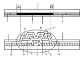
FIG. 2 is a schematic view of a TFT-LCD according to an embodiment of the invention. As shown in FIG. 2, the TFT-LCD according to the embodiment of the invention comprises an array substrate 100, a color filter substrate 200 and a liquid crystal layer (not shown) formed between the array substrate 100 and the color filter substrate 200. The array substrate 100 comprises a first substrate 11, a black matrix 1 formed on the first substrate 11, and a thin film transistor (TFT) device 13′ formed on the black matrix 1. The TFT device is a top gate TFT device which has a gate electrode 6 formed on a side facing away from the black matrix 1. The color filter substrate 200 comprises a second substrate 12 and a color filter layer 9 formed on the second substrate 12. The color filter layer 9 may include red, green and blue color filters. The color filter substrate 200 further comprises a counter electrode 8 formed on the color filter layer 9. The counter electrode 8 may be formed of transparent conductive materials such as indium tin oxide (ITO). The first substrate 11 and the second substrate 12 may be formed of glass, for example.
The top gate TFT device 13′ comprises: an active layer 2 formed on the black matrix 1; an ohmic contact layer 3 optionally formed on the active layer 2; a source electrode 41 and a drain electrode 42 formed on a part of the ohmic contact layer 3; an insulating layer 5 formed above the active layer 2 and covering the source electrode 41 and the drain electrode 42; and the gate electrode 6 formed on the insulating layer 5 between the source electrode 41 and the drain electrode 42. The array substrate 100 further comprises a pixel electrode 7 which is connected to the drain electrode 42 through a via hole 15 in the insulating layer 5. The pixel electrode 7 may be formed of indium tin oxide (ITO), for example. The area occupied by the top gate TFT device 13′ on the first substrate 11 is contained within the area occupied by the black matrix 1 on the first substrate 11. Further, TFT device 13′ and the black matrix 1 may occupy a same area on the first substrate 11. That is, in the embodiment of the invention, it is sufficient to make the black matrix 1 just cover the TFT device 13′ in order to prevent light leakage, without any substantial overlaps (d1, d2 portion shown in FIG. 1) between the area occupied by the black matrix 1 and the area occupied by the pixel electrode 7 in the conventional liquid crystal display as shown in FIG. 1. Therefore, the aperture ratio is improved. Additionally, according to the embodiment of the invention, the overlap (d as shown in FIG. 2) between the color filter (R, G or B) in the color filter substrate 200 and the TFT device 13′ in the array substrate 100 can be increased, thereby reducing manufacturing difficulty and lowering requirements for assembling accuracy. Moreover, according to the embodiment of the invention, the black matrix is not formed in the color filter substrate, therefore the requirement for process accuracy is less stringent and the process is simpler.
FIGS. 3-5 show flow charts of a method of manufacturing liquid crystal display according to an embodiment of the invention. As shown in FIG. 3, the method comprises steps of preparing an array substrate (301), preparing a color filter substrate (302) and assembling the array substrate and the color filter substrate and injecting liquid crystal material between the array substrate and the color filter substrate (303). As shown in FIG. 4, the step of preparing the array substrate comprises steps of providing a first substrate (401); forming a black matrix on the first substrate (402) and forming a thin film transistor (TFT) device on the black matrix (403). The TFT device is a top gate TFT device having a gate electrode formed on a side of the TFT device facing away the black matrix. As shown in FIG. 5, the step of preparing the color filter substrate comprises steps of providing a second substrate (501) and forming a color filter layer on the second substrate (502).
According to the embodiment of the invention, the steps of forming the black matrix and the TFT device on the first substrate comprises the following steps, as shown in FIGS. 6-9.
As shown in FIG. 6, a stack layer including a black matrix layer 1, an active layer 2, an optional ohmic contact layer 3 and an electrode layer 4 is formed successively in this order on the first substrate 11. As shown in FIG. 7, a photoresist layer 21 is formed on the stack layer; and the photoresist layer is patterned using a half tone mask M by photolithography and etching processes so as to remove the photoresist outside an area where the black matrix will be formed. The patterned photoresist layer 22 is formed with a first thickness in an area where the gate electrode 6 will be formed and a second thickness in the area of the black matrix area outside the gate electrode area. The first thickness is less than the second thickness.
As shown in FIG. 8, the stack layer outside the black matrix area is etched off using the patterned photoresist layer 22 so as to pattern the stack layer. Then the photoresist layer 22 is thinned by the first thickness. Next, the electrode layer 4 is patterned using the remained photoresist layer 23 so as to form a source electrode 41 and a drain electrode 42 separated from each other and expose the channel area between the source electrode 41 and the drain electrode 42. Then as shown in FIG. 9, the remained photoresist layer 23 is removed by an ashing process. Next, an insulating layer 5 may be deposited on the resulting structure, and a gate electrode 6 may be formed on the insulating layer 5 between the source electrode 41 and the drain electrode 42. In addition, via holes may be formed in the insulating layer 5 above the source electrode 41 by a conventional mask process, so as to further form a pixel electrode 7 connected to the source electrode 41.
According to the embodiments of the invention, in the array substrate, the black matrix is formed under the top gate TFT device (BM Under TFT), which reduces the overlap area of the black matrix and the pixel electrode. With the BM Under TFT structure as described above, the black matrix formed at the bottom blocks lights from a back light source unit disposed below. The gate electrode located on the top of the top gate TFT may also prevent the reflected light from interfering with the active layer (a-Si). Due to these two aspects, the aperture ratio of TFT-LCD is increased. According to the embodiments of the invention, in the color filter substrate, the formation process of the black matrix may be omitted, instead the color filter layer of R, G, B pixels can be formed directly on the glass substrate. Without considerations for the black matrix, the area of the pixel region can be larger, and the requirement for accuracy is lowered, and the process is simpler.
In addition, according to the manufacturing method of the embodiment of the invention, the manufacturing process of TFT substrate is simplified to a 4Mask process. This will reduce exposure processes and save the cost.
The embodiment of the invention being thus described, it will be obvious that the same may be varied in many ways. Such variations are not to be regarded as a departure from the spirit and scope of the invention, and all such modifications as would be obvious to those skilled in the art are intended to be included within the scope of the following claims.

Claims (14)

What is claimed is:
1. A liquid crystal display comprising:
an array substrate comprising:
a first substrate;
a black matrix formed on the first substrate; and
a thin film transistor (TFT) device formed on the black matrix, wherein the TFT device is a top gate TFT device having a gate electrode formed on a side of the TFT device facing away the black matrix and an active layer made of a-Si;
a color filter substrate comprising:
a second substrate; and
a color filter layer formed on the second substrate; and
a liquid crystal layer formed between the array substrate and the color filter substrate,
wherein the color filter substrate does not include a black matrix,
the TFT device comprises:
an active layer formed on the black matrix;
a source electrode and a drain electrode formed on respective parts of the active layer;
an insulating layer formed above the active layer and covering the source electrode and the drain electrode;
the gate electrode formed on the insulating layer between the source electrode and the drain electrode.
2. The liquid crystal display as set forth in claim 1, wherein the array substrate further comprises a pixel electrode formed on the insulating layer and connected with the source electrode through via holes in the insulating layer.
3. The liquid crystal display as set forth in claim 2, wherein the pixel electrode is formed of indium tin oxide (ITO).
4. The liquid crystal display as set forth in claim 1, wherein the TFT device further comprises an ohmic contact layer formed between the source electrode and the active layer and/or between the drain electrode and the active layer.
5. The liquid crystal display as set forth in claim 1, wherein an area occupied by the TFT device on the first substrate is contained within an area occupied by the black matrix on the first substrate.
6. The liquid crystal display as set forth in claim 5, wherein the TFT device and the black matrix occupy the same area on the first substrate.
7. The liquid crystal display as set forth in claim 1, wherein the color filter substrate further comprises a counter electrode formed on the color filter layer.
8. The liquid crystal display as set forth in claim 7, wherein the counter electrode is formed from indium tin oxide (ITO).
9. The liquid crystal display as set forth in claim 1, wherein the first substrate and the second substrate are formed of glass.
10. A method of manufacturing liquid crystal display comprising steps of:
preparing an array substrate comprising steps of:
providing a first substrate;
forming a black matrix on the first substrate and forming a thin film transistor(TFT) device on the black matrix, wherein the TFT device is a top gate TFT device having a gate electrode formed on a side of the TFT device facing away the black matrix and an active layer made of a-Si;
preparing a color filter substrate comprising steps of:
providing a second substrate; and
forming a color filter layer on the second substrate; and
assembling the array substrate and the color filter substrate and injecting liquid crystal between the array substrate and the color filter substrate,
wherein the color filter substrate does not include a black matrix,
the step of forming the black matrix and the TFT device on the first substrate comprises:
forming a stack layer including a black matrix layer, an active layer and an electrode layer in this order on the first substrate;
forming a photoresist layer on the stack layer;
patterning the photoresist layer using a half tone mask by a lithography and etching, so as to remove the photoresist layer outside an area where the black matrix is formed, and the patterned photoresist layer is formed with a first thickness in a first area where the gate electrode of the TFT device is formed and a second thickness in a second area outside the first area, wherein the first thickness is less than the second thickness;
etching off the stack layer outside the black matrix area using the patterned photoresist layer so as to pattern the stack layer;
removing the patterned photoresist layer by the first thickness, and forming separate source electrode and drain electrode using remained photoresist layer;
removing the remained photoresist layer by ashing, and depositing an insulating layer on resulting structure; and
forming a gate electrode on the insulating layer between the source electrode and the drain electrode.
11. The method as set forth in claim 10, wherein said step of preparing array substrate further comprises forming a pixel electrode which is formed on the insulating layer and connected with the source electrode through via holes in the insulating layer.
12. The method as set forth in claim 10, wherein the step of forming the black matrix and the TFT device on the first substrate further comprises forming an ohmic contact layer between the source electrode and the active layer and/or between the drain electrode and the active layer.
13. The method as set forth in claim 10, wherein an area occupied by the TFT device on the first substrate is contained within an area occupied by the black matrix on the first substrate.
14. The method as set forth in claim 13, wherein the TFT device and the black matrix occupy a same area on the first substrate.
US13/403,297 2011-03-29 2012-02-23 Liquid crystal display device in which array substrate includes black matrix and method of manufacturing the same Active 2033-05-13 US9036106B2 (en)

Applications Claiming Priority (2)

Application Number Priority Date Filing Date Title
CN201110076578.1 2011-03-29
CN201110076578.1A CN102645799B (en) 2011-03-29 2011-03-29 Liquid crystal display device, array substrate and color-film substrate as well as manufacturing methods thereof

Publications (2)

Publication Number Publication Date
US20120249936A1 US20120249936A1 (en) 2012-10-04
US9036106B2 true US9036106B2 (en) 2015-05-19

Family

ID=46658706

Family Applications (1)

Application Number Title Priority Date Filing Date
US13/403,297 Active 2033-05-13 US9036106B2 (en) 2011-03-29 2012-02-23 Liquid crystal display device in which array substrate includes black matrix and method of manufacturing the same

Country Status (2)

Country Link
US (1) US9036106B2 (en)
CN (1) CN102645799B (en)

Cited By (1)

* Cited by examiner, † Cited by third party
Publication number Priority date Publication date Assignee Title
US12265293B2 (en) * 2021-06-15 2025-04-01 Beijing Boe Technology Development Co., Ltd. Display panel and preparation method therefor, and display device

Families Citing this family (15)

* Cited by examiner, † Cited by third party
Publication number Priority date Publication date Assignee Title
US10199507B2 (en) * 2012-12-03 2019-02-05 Lg Display Co., Ltd. Thin film transistor, display device and method of manufacturing the same
CN103149760B (en) * 2013-02-19 2015-03-11 合肥京东方光电科技有限公司 Thin film transistor array substrate, manufacturing method and display device
US9530808B2 (en) * 2013-09-12 2016-12-27 Boe Technology Group Co., Ltd. TFT array substrate, manufacturing method thereof, and display device
CN103592801A (en) * 2013-11-19 2014-02-19 合肥京东方光电科技有限公司 Top grid type TFT array substrate, manufacturing method thereof, display panel and display device
CN103715137B (en) 2013-12-26 2018-02-06 京东方科技集团股份有限公司 Array base palte and its manufacture method, display device
JP2016157072A (en) * 2015-02-26 2016-09-01 株式会社ジャパンディスプレイ Display device
CN104950541B (en) * 2015-07-20 2018-05-01 深圳市华星光电技术有限公司 BOA type liquid crystal display panels and preparation method thereof
CN105045006B (en) * 2015-08-17 2017-10-24 武汉华星光电技术有限公司 A kind of liquid crystal display panel
KR102558900B1 (en) 2015-10-23 2023-07-25 엘지디스플레이 주식회사 Display Device and Method of Manufacturing the same
CN105445992A (en) * 2015-12-02 2016-03-30 小米科技有限责任公司 Liquid crystal display assembly and electronic equipment
CN106653688B (en) 2016-12-30 2019-10-18 惠科股份有限公司 method for manufacturing active array substrate
CN106647003B (en) * 2017-01-18 2020-04-21 京东方科技集团股份有限公司 A display device and display method
KR102583813B1 (en) * 2017-12-13 2023-09-26 엘지디스플레이 주식회사 Display apparatus
US20190355836A1 (en) * 2018-05-21 2019-11-21 Wuhan China Star Optoelectronics Technology Co., Ltd. Manufacturing method for amorphous silicon tft substrate
CN110289214A (en) * 2019-05-15 2019-09-27 友达光电(昆山)有限公司 Display device and manufacturing method of thin film transistor

Citations (8)

* Cited by examiner, † Cited by third party
Publication number Priority date Publication date Assignee Title
JPS58159520A (en) 1982-03-18 1983-09-21 Seiko Epson Corp Liquid crystal display panel
US6174754B1 (en) 2000-03-17 2001-01-16 Taiwan Semiconductor Manufacturing Company Methods for formation of silicon-on-insulator (SOI) and source/drain-on-insulator(SDOI) transistors
US20010019130A1 (en) 1998-05-15 2001-09-06 Semiconductor Energy Laboratory Co., Ltd. Semiconductor device
US20020024622A1 (en) 1996-10-16 2002-02-28 Seiko Epson Corporation Light shielding structure of a substrate for a liquid crystal device, liquid crystal device and projection type display device
US20040125261A1 (en) * 2002-12-17 2004-07-01 Dong-Hoon Lee Array substrate for LCD and method of fabricating the same
US20070064179A1 (en) 2005-09-20 2007-03-22 Lg Philips Lcd Co., Ltd. Liquid crystal display device and method of fabricating the same
CN1936650A (en) 2005-09-20 2007-03-28 蔡森尧 Refill wipe pack
CN101728436A (en) 2009-12-03 2010-06-09 友达光电股份有限公司 Element of thin film transistor and manufacturing method thereof

Family Cites Families (1)

* Cited by examiner, † Cited by third party
Publication number Priority date Publication date Assignee Title
FR2732781B1 (en) * 1995-04-07 1997-06-20 Thomson Lcd METHOD FOR MANUFACTURING TFT ACTIVE MATRIX FOR PROJECTION SYSTEM SCREEN

Patent Citations (9)

* Cited by examiner, † Cited by third party
Publication number Priority date Publication date Assignee Title
JPS58159520A (en) 1982-03-18 1983-09-21 Seiko Epson Corp Liquid crystal display panel
US20020024622A1 (en) 1996-10-16 2002-02-28 Seiko Epson Corporation Light shielding structure of a substrate for a liquid crystal device, liquid crystal device and projection type display device
CN101089709A (en) 1996-10-16 2007-12-19 精工爱普生株式会社 Substrate for liquid crystal device, liquid crystal device, and projection display device
US20010019130A1 (en) 1998-05-15 2001-09-06 Semiconductor Energy Laboratory Co., Ltd. Semiconductor device
US6174754B1 (en) 2000-03-17 2001-01-16 Taiwan Semiconductor Manufacturing Company Methods for formation of silicon-on-insulator (SOI) and source/drain-on-insulator(SDOI) transistors
US20040125261A1 (en) * 2002-12-17 2004-07-01 Dong-Hoon Lee Array substrate for LCD and method of fabricating the same
US20070064179A1 (en) 2005-09-20 2007-03-22 Lg Philips Lcd Co., Ltd. Liquid crystal display device and method of fabricating the same
CN1936650A (en) 2005-09-20 2007-03-28 蔡森尧 Refill wipe pack
CN101728436A (en) 2009-12-03 2010-06-09 友达光电股份有限公司 Element of thin film transistor and manufacturing method thereof

Non-Patent Citations (2)

* Cited by examiner, † Cited by third party
Title
First Chinese Office Action dated Jan. 27, 2014; Appln. No. 201110076578.1.
Second Chinese Office Action Issued Aug. 8, 2014; Appln. No. 201110076578.1.

Cited By (1)

* Cited by examiner, † Cited by third party
Publication number Priority date Publication date Assignee Title
US12265293B2 (en) * 2021-06-15 2025-04-01 Beijing Boe Technology Development Co., Ltd. Display panel and preparation method therefor, and display device

Also Published As

Publication number Publication date
CN102645799B (en) 2015-01-07
CN102645799A (en) 2012-08-22
US20120249936A1 (en) 2012-10-04

Similar Documents

Publication Publication Date Title
US9036106B2 (en) Liquid crystal display device in which array substrate includes black matrix and method of manufacturing the same
US20070070266A1 (en) Liquid crystal display device
US9952479B2 (en) Display substrate and method for fabricating the same, display panel and display device
CN104360557A (en) Array substrate, manufacturing method thereof and display device
KR101622655B1 (en) Liquid crystal display device and method of fabricating the same
US7602452B2 (en) Liquid crystal display device and method for manufacturing the same
US8698148B2 (en) Display devices and fabrication methods thereof
US20180045993A1 (en) Liquid crystal display device
US20090166633A1 (en) Array substrate and method for manufacturing the same
KR101799938B1 (en) Liquid crystal display device
CN102044490B (en) Fabricating method of thin film transistor array substrate
KR101955992B1 (en) Array substrate for fringe field switching mode liquid crystal display device and method for fabricating the same
US20170005119A1 (en) Manufacturing method of thin film transistor substrate
KR101849569B1 (en) Thin film transistor substrate and method of fabricating the same
US10503034B2 (en) Manufacturing method of a TFT substrate and structure
US11442319B2 (en) Display substrate, display apparatus, and method of fabricating display substrate
US9780221B2 (en) Thin film transistor substrate comprising a photoresist layer formed between a first dielectric layer and an amorphous silicon layer
CN210325797U (en) Array substrate and display panel
KR101590381B1 (en) Liquid crystal display device and Method of fabricating the same
JP5275650B2 (en) Liquid crystal display
KR100643559B1 (en) Array substrate for liquid crystal display device and manufacturing method
US8435722B2 (en) Method for fabricating liquid crystal display device
US9128313B2 (en) Method of manufacturing liquid crystal display
KR20080042466A (en) LCD panel and manufacturing method
KR20080062647A (en) Thin film transistor array substrate and its manufacturing method

Legal Events

Date Code Title Description
AS Assignment

Owner name: BOE TECHNOLOGY GROUP CO., LTD., CHINA

Free format text: ASSIGNMENT OF ASSIGNORS INTEREST;ASSIGNORS:ZI, YUBAO;JUNG, JAEYUN;WANG, SHIKAI;AND OTHERS;SIGNING DATES FROM 20120206 TO 20120208;REEL/FRAME:027751/0830

Owner name: HEFEI BOE OPTOELECTRONICS TECHNOLOGY CO., LTD., CH

Free format text: ASSIGNMENT OF ASSIGNORS INTEREST;ASSIGNORS:ZI, YUBAO;JUNG, JAEYUN;WANG, SHIKAI;AND OTHERS;SIGNING DATES FROM 20120206 TO 20120208;REEL/FRAME:027751/0830

STCF Information on status: patent grant

Free format text: PATENTED CASE

MAFP Maintenance fee payment

Free format text: PAYMENT OF MAINTENANCE FEE, 4TH YEAR, LARGE ENTITY (ORIGINAL EVENT CODE: M1551); ENTITY STATUS OF PATENT OWNER: LARGE ENTITY

Year of fee payment: 4

MAFP Maintenance fee payment

Free format text: PAYMENT OF MAINTENANCE FEE, 8TH YEAR, LARGE ENTITY (ORIGINAL EVENT CODE: M1552); ENTITY STATUS OF PATENT OWNER: LARGE ENTITY

Year of fee payment: 8