US9035357B2 - Compound semiconductor device and manufacturing method therefor - Google Patents
Compound semiconductor device and manufacturing method therefor Download PDFInfo
- Publication number
- US9035357B2 US9035357B2 US14/202,279 US201414202279A US9035357B2 US 9035357 B2 US9035357 B2 US 9035357B2 US 201414202279 A US201414202279 A US 201414202279A US 9035357 B2 US9035357 B2 US 9035357B2
- Authority
- US
- United States
- Prior art keywords
- compound semiconductor
- opening
- protective film
- lower layer
- semiconductor layer
- Prior art date
- Legal status (The legal status is an assumption and is not a legal conclusion. Google has not performed a legal analysis and makes no representation as to the accuracy of the status listed.)
- Active
Links
- 239000004065 semiconductor Substances 0.000 title claims abstract description 70
- 150000001875 compounds Chemical class 0.000 title claims abstract description 65
- 238000004519 manufacturing process Methods 0.000 title description 10
- 229910052581 Si3N4 Inorganic materials 0.000 claims abstract description 26
- HQVNEWCFYHHQES-UHFFFAOYSA-N silicon nitride Chemical compound N12[Si]34N5[Si]62N3[Si]51N64 HQVNEWCFYHHQES-UHFFFAOYSA-N 0.000 claims abstract description 26
- 230000001681 protective effect Effects 0.000 claims abstract description 23
- IJGRMHOSHXDMSA-UHFFFAOYSA-N Atomic nitrogen Chemical compound N#N IJGRMHOSHXDMSA-UHFFFAOYSA-N 0.000 claims description 12
- 229910021420 polycrystalline silicon Inorganic materials 0.000 claims description 9
- 229920005591 polysilicon Polymers 0.000 claims description 9
- 238000013459 approach Methods 0.000 claims description 7
- 229910052757 nitrogen Inorganic materials 0.000 claims description 6
- 125000004433 nitrogen atom Chemical group N* 0.000 claims description 4
- 239000000758 substrate Substances 0.000 abstract description 8
- 229910002704 AlGaN Inorganic materials 0.000 description 49
- 238000002161 passivation Methods 0.000 description 49
- 239000007789 gas Substances 0.000 description 20
- 238000000034 method Methods 0.000 description 18
- 230000005684 electric field Effects 0.000 description 13
- 230000006866 deterioration Effects 0.000 description 9
- 238000005530 etching Methods 0.000 description 9
- 230000008569 process Effects 0.000 description 8
- 230000005764 inhibitory process Effects 0.000 description 7
- 239000000203 mixture Substances 0.000 description 7
- 238000002955 isolation Methods 0.000 description 6
- 238000001039 wet etching Methods 0.000 description 6
- BLRPTPMANUNPDV-UHFFFAOYSA-N Silane Chemical compound [SiH4] BLRPTPMANUNPDV-UHFFFAOYSA-N 0.000 description 5
- 229910052782 aluminium Inorganic materials 0.000 description 5
- KRHYYFGTRYWZRS-UHFFFAOYSA-N Fluorane Chemical compound F KRHYYFGTRYWZRS-UHFFFAOYSA-N 0.000 description 4
- XUIMIQQOPSSXEZ-UHFFFAOYSA-N Silicon Chemical compound [Si] XUIMIQQOPSSXEZ-UHFFFAOYSA-N 0.000 description 4
- 238000010586 diagram Methods 0.000 description 4
- 229910052751 metal Inorganic materials 0.000 description 4
- 239000002184 metal Substances 0.000 description 4
- 150000004767 nitrides Chemical class 0.000 description 4
- 238000005268 plasma chemical vapour deposition Methods 0.000 description 4
- 230000010287 polarization Effects 0.000 description 4
- 229910052710 silicon Inorganic materials 0.000 description 4
- 239000010703 silicon Substances 0.000 description 4
- 230000008901 benefit Effects 0.000 description 3
- 239000000872 buffer Substances 0.000 description 3
- 238000001312 dry etching Methods 0.000 description 3
- 230000005533 two-dimensional electron gas Effects 0.000 description 3
- DDFHBQSCUXNBSA-UHFFFAOYSA-N 5-(5-carboxythiophen-2-yl)thiophene-2-carboxylic acid Chemical compound S1C(C(=O)O)=CC=C1C1=CC=C(C(O)=O)S1 DDFHBQSCUXNBSA-UHFFFAOYSA-N 0.000 description 2
- QGZKDVFQNNGYKY-UHFFFAOYSA-N Ammonia Chemical compound N QGZKDVFQNNGYKY-UHFFFAOYSA-N 0.000 description 2
- XKRFYHLGVUSROY-UHFFFAOYSA-N Argon Chemical compound [Ar] XKRFYHLGVUSROY-UHFFFAOYSA-N 0.000 description 2
- SECXISVLQFMRJM-UHFFFAOYSA-N N-Methylpyrrolidone Chemical compound CN1CCCC1=O SECXISVLQFMRJM-UHFFFAOYSA-N 0.000 description 2
- 238000004380 ashing Methods 0.000 description 2
- QVGXLLKOCUKJST-UHFFFAOYSA-N atomic oxygen Chemical compound [O] QVGXLLKOCUKJST-UHFFFAOYSA-N 0.000 description 2
- 230000015572 biosynthetic process Effects 0.000 description 2
- 239000007853 buffer solution Substances 0.000 description 2
- 230000015556 catabolic process Effects 0.000 description 2
- 230000008859 change Effects 0.000 description 2
- 239000003814 drug Substances 0.000 description 2
- 229940079593 drug Drugs 0.000 description 2
- 230000000694 effects Effects 0.000 description 2
- 238000010893 electron trap Methods 0.000 description 2
- 230000005669 field effect Effects 0.000 description 2
- 230000006872 improvement Effects 0.000 description 2
- 238000009413 insulation Methods 0.000 description 2
- 239000012212 insulator Substances 0.000 description 2
- 230000003647 oxidation Effects 0.000 description 2
- 238000007254 oxidation reaction Methods 0.000 description 2
- 239000001301 oxygen Substances 0.000 description 2
- 229910052760 oxygen Inorganic materials 0.000 description 2
- 239000000243 solution Substances 0.000 description 2
- 230000002269 spontaneous effect Effects 0.000 description 2
- JLTRXTDYQLMHGR-UHFFFAOYSA-N trimethylaluminium Chemical compound C[Al](C)C JLTRXTDYQLMHGR-UHFFFAOYSA-N 0.000 description 2
- XCZXGTMEAKBVPV-UHFFFAOYSA-N trimethylgallium Chemical compound C[Ga](C)C XCZXGTMEAKBVPV-UHFFFAOYSA-N 0.000 description 2
- VYPSYNLAJGMNEJ-UHFFFAOYSA-N Silicium dioxide Chemical compound O=[Si]=O VYPSYNLAJGMNEJ-UHFFFAOYSA-N 0.000 description 1
- 230000004075 alteration Effects 0.000 description 1
- 229910052786 argon Inorganic materials 0.000 description 1
- 239000007772 electrode material Substances 0.000 description 1
- 238000001704 evaporation Methods 0.000 description 1
- 230000008020 evaporation Effects 0.000 description 1
- 239000008246 gaseous mixture Substances 0.000 description 1
- 239000012535 impurity Substances 0.000 description 1
- 239000011261 inert gas Substances 0.000 description 1
- 238000002347 injection Methods 0.000 description 1
- 239000007924 injection Substances 0.000 description 1
- 239000000463 material Substances 0.000 description 1
- 238000002156 mixing Methods 0.000 description 1
- 238000001451 molecular beam epitaxy Methods 0.000 description 1
- 239000012299 nitrogen atmosphere Substances 0.000 description 1
- 230000008520 organization Effects 0.000 description 1
- 229920006395 saturated elastomer Polymers 0.000 description 1
- 229910052814 silicon oxide Inorganic materials 0.000 description 1
- 238000004528 spin coating Methods 0.000 description 1
- 239000000126 substance Substances 0.000 description 1
- 238000006467 substitution reaction Methods 0.000 description 1
- 238000000927 vapour-phase epitaxy Methods 0.000 description 1
Images


Classifications
-
- H—ELECTRICITY
- H01—ELECTRIC ELEMENTS
- H01L—SEMICONDUCTOR DEVICES NOT COVERED BY CLASS H10
- H01L29/00—Semiconductor devices specially adapted for rectifying, amplifying, oscillating or switching and having potential barriers; Capacitors or resistors having potential barriers, e.g. a PN-junction depletion layer or carrier concentration layer; Details of semiconductor bodies or of electrodes thereof ; Multistep manufacturing processes therefor
- H01L29/40—Electrodes ; Multistep manufacturing processes therefor
- H01L29/408—Electrodes ; Multistep manufacturing processes therefor with an insulating layer with a particular dielectric or electrostatic property, e.g. with static charges or for controlling trapped charges or moving ions, or with a plate acting on the insulator potential or the insulator charges, e.g. for controlling charges effect or potential distribution in the insulating layer, or with a semi-insulating layer contacting directly the semiconductor surface
-
- H—ELECTRICITY
- H01—ELECTRIC ELEMENTS
- H01L—SEMICONDUCTOR DEVICES NOT COVERED BY CLASS H10
- H01L29/00—Semiconductor devices specially adapted for rectifying, amplifying, oscillating or switching and having potential barriers; Capacitors or resistors having potential barriers, e.g. a PN-junction depletion layer or carrier concentration layer; Details of semiconductor bodies or of electrodes thereof ; Multistep manufacturing processes therefor
- H01L29/66—Types of semiconductor device ; Multistep manufacturing processes therefor
- H01L29/66007—Multistep manufacturing processes
- H01L29/66075—Multistep manufacturing processes of devices having semiconductor bodies comprising group 14 or group 13/15 materials
- H01L29/66227—Multistep manufacturing processes of devices having semiconductor bodies comprising group 14 or group 13/15 materials the devices being controllable only by the electric current supplied or the electric potential applied, to an electrode which does not carry the current to be rectified, amplified or switched, e.g. three-terminal devices
- H01L29/66409—Unipolar field-effect transistors
- H01L29/66446—Unipolar field-effect transistors with an active layer made of a group 13/15 material, e.g. group 13/15 velocity modulation transistor [VMT], group 13/15 negative resistance FET [NERFET]
- H01L29/66462—Unipolar field-effect transistors with an active layer made of a group 13/15 material, e.g. group 13/15 velocity modulation transistor [VMT], group 13/15 negative resistance FET [NERFET] with a heterojunction interface channel or gate, e.g. HFET, HIGFET, SISFET, HJFET, HEMT
-
- H—ELECTRICITY
- H01—ELECTRIC ELEMENTS
- H01L—SEMICONDUCTOR DEVICES NOT COVERED BY CLASS H10
- H01L29/00—Semiconductor devices specially adapted for rectifying, amplifying, oscillating or switching and having potential barriers; Capacitors or resistors having potential barriers, e.g. a PN-junction depletion layer or carrier concentration layer; Details of semiconductor bodies or of electrodes thereof ; Multistep manufacturing processes therefor
- H01L29/66—Types of semiconductor device ; Multistep manufacturing processes therefor
- H01L29/68—Types of semiconductor device ; Multistep manufacturing processes therefor controllable by only the electric current supplied, or only the electric potential applied, to an electrode which does not carry the current to be rectified, amplified or switched
- H01L29/76—Unipolar devices, e.g. field effect transistors
- H01L29/772—Field effect transistors
- H01L29/778—Field effect transistors with two-dimensional charge carrier gas channel, e.g. HEMT ; with two-dimensional charge-carrier layer formed at a heterojunction interface
- H01L29/7786—Field effect transistors with two-dimensional charge carrier gas channel, e.g. HEMT ; with two-dimensional charge-carrier layer formed at a heterojunction interface with direct single heterostructure, i.e. with wide bandgap layer formed on top of active layer, e.g. direct single heterostructure MIS-like HEMT
- H01L29/7787—Field effect transistors with two-dimensional charge carrier gas channel, e.g. HEMT ; with two-dimensional charge-carrier layer formed at a heterojunction interface with direct single heterostructure, i.e. with wide bandgap layer formed on top of active layer, e.g. direct single heterostructure MIS-like HEMT with wide bandgap charge-carrier supplying layer, e.g. direct single heterostructure MODFET
-
- H—ELECTRICITY
- H02—GENERATION; CONVERSION OR DISTRIBUTION OF ELECTRIC POWER
- H02M—APPARATUS FOR CONVERSION BETWEEN AC AND AC, BETWEEN AC AND DC, OR BETWEEN DC AND DC, AND FOR USE WITH MAINS OR SIMILAR POWER SUPPLY SYSTEMS; CONVERSION OF DC OR AC INPUT POWER INTO SURGE OUTPUT POWER; CONTROL OR REGULATION THEREOF
- H02M7/00—Conversion of ac power input into dc power output; Conversion of dc power input into ac power output
- H02M7/42—Conversion of dc power input into ac power output without possibility of reversal
- H02M7/44—Conversion of dc power input into ac power output without possibility of reversal by static converters
- H02M7/48—Conversion of dc power input into ac power output without possibility of reversal by static converters using discharge tubes with control electrode or semiconductor devices with control electrode
- H02M7/53—Conversion of dc power input into ac power output without possibility of reversal by static converters using discharge tubes with control electrode or semiconductor devices with control electrode using devices of a triode or transistor type requiring continuous application of a control signal
- H02M7/537—Conversion of dc power input into ac power output without possibility of reversal by static converters using discharge tubes with control electrode or semiconductor devices with control electrode using devices of a triode or transistor type requiring continuous application of a control signal using semiconductor devices only, e.g. single switched pulse inverters
-
- H—ELECTRICITY
- H01—ELECTRIC ELEMENTS
- H01L—SEMICONDUCTOR DEVICES NOT COVERED BY CLASS H10
- H01L29/00—Semiconductor devices specially adapted for rectifying, amplifying, oscillating or switching and having potential barriers; Capacitors or resistors having potential barriers, e.g. a PN-junction depletion layer or carrier concentration layer; Details of semiconductor bodies or of electrodes thereof ; Multistep manufacturing processes therefor
- H01L29/02—Semiconductor bodies ; Multistep manufacturing processes therefor
- H01L29/12—Semiconductor bodies ; Multistep manufacturing processes therefor characterised by the materials of which they are formed
- H01L29/20—Semiconductor bodies ; Multistep manufacturing processes therefor characterised by the materials of which they are formed including, apart from doping materials or other impurities, only AIIIBV compounds
- H01L29/2003—Nitride compounds
-
- H—ELECTRICITY
- H01—ELECTRIC ELEMENTS
- H01L—SEMICONDUCTOR DEVICES NOT COVERED BY CLASS H10
- H01L29/00—Semiconductor devices specially adapted for rectifying, amplifying, oscillating or switching and having potential barriers; Capacitors or resistors having potential barriers, e.g. a PN-junction depletion layer or carrier concentration layer; Details of semiconductor bodies or of electrodes thereof ; Multistep manufacturing processes therefor
- H01L29/66—Types of semiconductor device ; Multistep manufacturing processes therefor
- H01L29/68—Types of semiconductor device ; Multistep manufacturing processes therefor controllable by only the electric current supplied, or only the electric potential applied, to an electrode which does not carry the current to be rectified, amplified or switched
- H01L29/76—Unipolar devices, e.g. field effect transistors
- H01L29/772—Field effect transistors
- H01L29/778—Field effect transistors with two-dimensional charge carrier gas channel, e.g. HEMT ; with two-dimensional charge-carrier layer formed at a heterojunction interface
- H01L29/7786—Field effect transistors with two-dimensional charge carrier gas channel, e.g. HEMT ; with two-dimensional charge-carrier layer formed at a heterojunction interface with direct single heterostructure, i.e. with wide bandgap layer formed on top of active layer, e.g. direct single heterostructure MIS-like HEMT
Definitions
- Embodiments relate to a compound semiconductor device and a manufacturing method for the compound semiconductor device.
- Nitride semiconductor devices include field-effect transistors.
- field-effect transistors particularly high electron mobility transistors (HEMTs).
- HEMTs high electron mobility transistors
- an AlGaN/GaN HEMT using GaN in an electron transit layer and AlGaN in an electron supply layer is attracting attention.
- an AlGaN/GaN HEMT distortion occurs in AlGaN due to the difference in lattice constants between GaN and AlGaN.
- Patent Literature 1 Japanese National Publication of International Patent Application No. 2009-524242
- Operating voltage needs to be increased in a nitride semiconductor device for high output and high frequency applications, such as an AlGaN/GaN HEMT, to obtain high power.
- An increase in operating voltage increases the electric field strength at and around a gate electrode and causes deterioration in device characteristics (chemical and physical changes).
- it is essential to inhibit deterioration in device characteristics caused by a high electric field at and around a gate electrode.
- An embodiment of a compound semiconductor device includes a compound semiconductor layer, a silicon nitride protective film having an opening and covering the compound semiconductor layer, and an electrode formed on the compound semiconductor layer so as to plug the opening.
- a lower layer portion of the protective film includes a portion (a projecting portion) projecting from a side surface of the opening.
- An embodiment of a method for manufacturing a compound semiconductor device includes forming a silicon nitride protective film on a compound semiconductor layer, forming an opening in the protective film, and forming an electrode on the compound semiconductor layer so as to plug the opening.
- the forming the opening includes forming the opening such that a lower layer portion of the protective film includes a projecting portion projecting from a side surface of the opening.
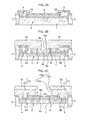
- FIGS. 1A to 1C are schematic sectional views illustrating, in the order of steps, a method for manufacturing a Schottky AlGaN/GaN HEMT according to a first embodiment
- FIGS. 2A to 2C are schematic sectional views illustrating, in the order of steps, the method for manufacturing the Schottky AlGaN/GaN HEMT according to the first embodiment, following FIGS. 1A to 10 ;
- FIGS. 3A and 3B are schematic sectional views illustrating, in the order of steps, the method for manufacturing the Schottky AlGaN/GaN HEMT according to the first embodiment, following FIGS. 2A to 2C ;
- FIG. 4 is a schematic sectional view illustrating, on an enlarged scale, a part of a passivation film formed in the step in FIG. 2A ;
- FIG. 5 is a schematic sectional view illustrating, on an enlarged scale, a part of an opening in the passivation film formed in the step in FIG. 2B ;
- FIGS. 6A and 6B are graphs illustrating results of checking characteristics of three terminals of the AlGaN/GaN HEMT according to the first embodiment on the basis of comparison with an AlGaN/GaN HEMT with the above-described conventional structure including the conventional passivation film;
- FIGS. 7A to 7C are schematic sectional views illustrating main steps of a method for manufacturing a Schottky AlGaN/GaN HEMT according to a second embodiment
- FIG. 8 is a schematic sectional view illustrating, on an enlarged scale, a part of a passivation film formed in the step in FIG. 7A ;
- FIG. 9 is a schematic sectional view illustrating, on an enlarged scale, a part of an opening in the passivation film formed in the step in FIG. 7B ;
- FIGS. 10A and 10B are graphs illustrating results of checking characteristics of three terminals of the AlGaN/GaN HEMT according to the second embodiment on the basis of comparison with the AlGaN/GaN HEMT with the above-described conventional structure including the conventional passivation film;
- FIG. 11 is a connection diagram illustrating the schematic configuration of a power supply unit according to a third embodiment.
- FIG. 12 is a connection diagram illustrating the schematic configuration of a high-frequency amplifier according to a fourth embodiment.
- the present embodiment discloses a Schottky AlGaN/GaN HEMT as a compound semiconductor device.
- FIGS. 1A to 3B are schematic sectional views illustrating, in the order of steps, a method for manufacturing a Schottky AlGaN/GaN HEMT according to the first embodiment.
- a compound semiconductor layer 2 which is a compound semiconductor laminated structure is first formed on, for example, a semi-insulating SiC substrate 1 as a growth substrate.
- the compound semiconductor layer 2 includes a buffer layer 2 a , an electron transit layer 2 b , an intermediate layer 2 c , an electron supply layer 2 d , and a cap layer 2 e .
- 2DEG two-dimensional electron gas
- MOVPE metal organic vapor phase epitaxy
- MBE Molecular beam epitaxy
- AlN, i-GaN (intentionally undoped GaN), i-AlGaN, n-AlGaN, and n-GaN are deposited in order on the SiC substrate 1 .
- the buffer layer 2 a , electron transit layer 2 b , intermediate layer 2 c , electron supply layer 2 d , and cap layer 2 e are stacked and formed.
- the growth conditions for AlN, GaN, and AlGaN are that a gaseous mixture of trimethyl aluminum gas, trimethyl gallium gas, and ammonia gas is used as a source gas, that whether to supply trimethyl aluminum gas as an Al source and trimethyl gallium gas as a Ga source and the flow rates of the gases are appropriately set according to a compound semiconductor layer to be grown, that the flow rates of ammonia gas as a common material are about 100 sccm to 10 slm, that the growth pressures for AlN, GaN, and AlGaN are about 50 to 300 Torr, and that the growth temperatures are about 1000 to 1200.degree. C.
- GaN or AlGaN
- SiH 4 gas containing an n-type impurity such as Si is added to a source gas at a predetermined flow rate, and GaN (or AlGaN) is doped with Si.
- the doping concentrations of Si are set to about 1 ⁇ 10 18 /cm 3 to 1 ⁇ 10 20 /cm 3 (e.g., 5 ⁇ 10 18 /cm 3 ).
- the buffer layer 2 a is formed to a thickness of about 0.1 ⁇ m
- the electron transit layer 2 b is formed to a thickness of about 3 ⁇ m
- the intermediate layer 2 c is formed to a thickness of about 5 nm
- the electron supply layer 2 d is formed to a thickness of about 20 nm with an Al ratio of, e.g., about 0.2 to 0.3
- the cap layer 2 e is formed to a thickness of about 10 nm.
- a device isolation structure 3 is formed.
- argon (Ar) is injected into a device isolation region of the compound semiconductor layer 2 .
- the device isolation structure 3 is formed at superficial portions of the compound semiconductor layer 2 and SiC substrate 1 .
- the device isolation structure 3 defines an active region on the compound semiconductor layer 2 .
- the device isolation may be performed by, e.g., shallow trench isolation (STI) instead of the injection.
- STI shallow trench isolation
- a source electrode 4 and a drain electrode 5 are formed.
- electrode grooves 2 A and 2 B are first formed in the cap layer 2 e , at positions where a source electrode and a drain electrode are to be formed at a surface of the compound semiconductor layer 2 .
- a resist mask having openings corresponding to the positions where the source electrode and drain electrode are to be formed at the surface of the compound semiconductor layer 2 is formed.
- the cap layer 2 e is partially removed by dry etching using the resist mask. With these processes, the electrode grooves 2 A and 2 B are formed.
- An inert gas such as Ar and a chlorinated gas such as Cl.sub.2 are used as etching gases in the dry etching.
- the electrode grooves may be formed by dry-etching the compound semiconductor layer 2 so as to penetrate the cap layer 2 e and reach a superficial portion of the electron supply layer 2 d.
- Ti and Al are used as examples of an electrode material.
- a double-layer resist with an overhang structure suitable for evaporation or lift-off is used to form the electrodes.
- the resist is applied to the compound semiconductor layer 2 to form the resist mask that is open so as to expose the electrode grooves 2 A and 2 B.
- Ti and Al are deposited while using the resist mask.
- the thickness of Ti is set to about 20 nm, and the thickness of Al is set to about 200 nm.
- the resist mask with the overhang structure and Ti and Al deposited on the resist mask are removed by lift-off. After that, the SiC substrate 1 is heat-treated at a temperature of about 550° C. in, for example, a nitrogen atmosphere.
- Remaining Ti and Al are made to form an ohmic contact with the electron supply layer 2 d .
- the source electrode 4 and drain electrode 5 which plug the electrode grooves 2 A and 2 B with lower portions of Ti and Al, are formed.
- a passivation film 6 for protecting the surface of the compound semiconductor layer 2 is formed.
- silicon nitride (a silicon nitride) is deposited across the surface of the compound semiconductor layer 2 to a thickness of, e.g., about 50 nm by plasma CVD or the like to form the passivation film 6 .
- a silicon nitride is a stable insulator and is suitably used for a protective film of the surface of the compound semiconductor layer 2 .
- FIG. 4 illustrates, on an enlarged scale, a part of the passivation film 6 .
- the percentage of nitrogen (N) vacancies of a lower layer portion 6 a in contact with the surface of the compound semiconductor layer 2 is higher than that of silicon nitride in stoichiometric condition (Si.sub.3N.sub.4).
- the passivation film 6 is formed so as to drastically and continuously approach stoichiometric condition toward the top. Note that although a boundary between the lower layer portion 6 a and the other portion is illustrated by a broken line for the sake of convenience, there is no clear boundary. If silicon nitride has “a high percentage of N vacancies,” this means in the present embodiment that the silicon nitride has a high composition ratio of Si.
- the percentage of N vacancies of the lower layer portion 6 a to N atoms of silicon nitride in stoichiometric condition is not more than 50% (X in Si 3 N x is not more than 2). If a portion extending downward from a point where the percentage of N vacancies is 50% in a thickness direction of the passivation film 6 is defined as the lower layer portion 6 a , the thickness of the lower layer portion 6 a is about 2 to 5 nm. If the thickness of the lower layer portion 6 a is less than 2 nm, the lower layer portion cannot provide sufficient efficacy (to be described later). If the thickness of the lower layer portion 6 a is more than nm, a gate leak current is larger.
- the lower layer portion 6 a Since the thickness of the lower layer portion 6 a is set to about 2 to 5 nm, the lower layer portion can provide sufficient efficacy (to be described later) without increasing a gate leak current.
- the lower layer portion 6 a is formed so as to have the percentage of N vacancies to N atoms of silicon nitride in stoichiometric condition set to, e.g., about 50% and a thickness of, e.g., about 3 nm.
- SiH.sub.4 gas and N.sub.2 gas are supplied at a flow rate of 5 sccm and at a flow rate of 100 sccm, respectively, into a film forming chamber for plasma CVD before electric discharge.
- RF waves 13.56 MHz, 50 W
- N 2 gas starts to be supplied at a flow rate of 200 sccm within 2 sec of the start of the introduction of SiH 4 gas (the flow rate of 200 sccm includes the earlier flow rate of 100 sccm).
- an opening 6 b is formed in the passivation film 6 .
- a resist is first applied to the entire surface of the passivation film 6 .
- the resist is subjected to exposure for an opening having a width of, e.g., 600 nm by the UV method and is developed. With these processes, a resist mask 10 having an opening 10 a is formed.
- the passivation film 6 is wet-etched by using the resist mask 10 .
- the wet etching is performed under the condition that the etching rate at the lower layer portion 6 a of the passivation film 6 is lower than that at the other portion.
- a buffer solution which is a mixture of hydrofluoric acid and ammonium fluoride is used as an etchant. With the wet etching, a portion exposed in the opening 10 a of the passivation film 6 is etched, and the opening 6 b is formed in the passivation film 6 .
- FIG. 5 illustrates, on an enlarged scale, the opening 6 b of the passivation film 6 .
- the passivation film 6 is isotropically etched by the wet etching, and the opening 6 b is formed so as to have a forward tapered side surface. Since the etching rate at the lower layer portion 6 a is lower than that at the other portion at the opening 6 b , a projecting portion 6 c projecting from the side surface of the opening 6 b is formed at the lower layer portion 6 a .
- the projecting portion 6 c is formed according to the etching rates so as to have a width of, e.g., about 10 nm. Since the projecting portion 6 c is a part of the lower layer portion 6 a and has a high percentage of N vacancies, silicon nitride at the projecting portion 6 c is oxidized to form silicon oxynitride.
- the resist mask 10 is removed by ashing using oxygen plasma or wet treatment using a drug solution.
- a resist mask 13 for gate formation is formed.
- a lower layer resist 11 e.g., the product named PMGI, manufactured by MicroChem Corp., USA
- an upper layer resist 12 e.g., the product named SUMIRESIST PFI32-A8, manufactured by Sumitomo Chemical Co., Ltd.
- An opening 12 a e.g., about 1.5 ⁇ m long is formed in the upper layer resist 12 by UV exposure.
- the lower layer resist 11 is wet-etched with an alkaline developer by using the upper layer resist 12 as a mask to form an opening 11 a in the lower layer resist 11 .
- the resist mask 13 including the lower layer resist 11 having the opening 11 a and the upper layer resist 12 having the opening 12 a is formed.
- an opening constituted by the openings 11 a and 12 a communicating with each other is denoted by reference characters 13 a.
- a gate electrode 7 is formed.
- a gate metal Ni with a thickness of about 10 nm and Au with a thickness of about 300 nm
- the gate electrode 7 is formed so as to plug the opening 6 b of the passivation film 6 with the gate metal and form a Schottky contact with the surface of the compound semiconductor layer 2 .
- the resist mask 13 is removed.
- the SiC substrate 1 is soaked in N-methylpyrrolidinone heated to 80° C., and the resist mask 13 and unnecessary portions of the gate metal are removed by lift-off.
- a lower portion of the gate electrode 7 forms a Schottky contact with the surface of the compound semiconductor layer 2 in the opening 6 b , and an upper portion is formed so as to be wider than the opening 6 b and has an overhanging shape.
- a Schottky AlGaN/GaN HEMT is formed.
- a conventional passivation film is of uniform elemental composition from an interface with a compound semiconductor layer to an upper surface of the passivation film.
- An opening in the passivation film where a gate electrode is to be formed has a side surface of monotonous shape and is of homogenous elemental composition.
- the passivation film 6 including the lower layer portion 6 a made of silicon nitride with many N vacancies (the percentage of which to N atoms of silicon nitride in stoichiometric condition is not less than 50%) and having a very small thickness (not more than 5 nm) is formed so as to be in contact with the surface of the compound semiconductor layer 2 .
- the percentage of N vacancies of the lower layer portion 6 a is higher than that of silicon nitride in stoichiometric condition (Si 3 N 4 ).
- the passivation film 6 is formed so as to drastically and continuously approach stoichiometric condition toward the top.
- the lower layer portion 6 a that is a silicon nitride film with many N vacancies, i.e., a silicon nitride film with many positive charges lowers the energy of the conduction band at the surface of the compound semiconductor layer 2 to reduce access resistance.
- the efficacy in lowering the energy of the conduction band blocks the influence of an electron trap at the surface of the compound semiconductor layer 2 to reduce current collapse.
- a part of the lower layer portion 6 a is formed as the projecting portion 6 c projecting from the side surface of the opening 6 b toward a Schottky interface, due to the low etching rate at the lower layer portion 6 a having many N vacancies and the very small thickness. Since the projecting portion 6 c has many N vacancies and is chemically active, the projecting portion 6 c is highly susceptible to oxidation. The projecting portion 6 c is likely to turn into a silicon oxynitride film and exhibits high insulation performance. The presence of the projecting portion 6 c reduces electric field concentration on an edge of the gate electrode 7 , inhibits the gate electrode 7 from being broken down due to a high electric field, and contributes to enhancement of the reliability of the device.
- FIGS. 6A and 6B illustrate results of the checking.
- FIG. 6A illustrates the result of the conventional structure while FIG. 6B illustrates the result of the present embodiment.
- the present embodiment was confirmed to have achieved significant improvement in terms of current collapse over the conventional structure.
- the present embodiment was also confirmed to have little change in gate current at a high-temperature current test and not to have a breakdown.
- a highly reliable Schottky AlGaN/GaN HEMT which achieves high voltage and high power by reducing electric field concentration on an electrode edge to ensure inhibition of deterioration in device characteristics as well as increasing operating voltage is achieved.
- a Schottky AlGaN/GaN HEMT according to the second embodiment will be described below.
- the present embodiment is different from the first embodiment in the configuration of a passivation film.
- the same components and the like as those of an AlGaN/GaN HEMT according to the first embodiment are denoted by the same reference numerals, and a detailed description thereof will be omitted.
- FIGS. 7A to 7C are schematic sectional views illustrating main steps of a method for manufacturing the Schottky AlGaN/GaN HEMT according to the second embodiment.
- the steps in FIGS. 1A to 1C according to the first embodiment are first performed to form a source electrode 4 and a drain electrode 5 on a compound semiconductor layer 2 .
- a passivation film 21 for protecting a surface of the compound semiconductor layer 2 is formed.
- silicon nitride (a silicon nitride) is deposited across the surface of the compound semiconductor layer 2 to a thickness of, e.g., about 50 nm by plasma CVD or the like to form the passivation film 21 .
- a silicon nitride is a stable insulator and is suitably used for a protective film of the surface of the compound semiconductor layer 2 .
- FIG. 8 illustrates, on an enlarged scale, a part of the passivation film 21 .
- a lower layer portion 21 a in contact with the surface of the compound semiconductor layer 2 is made of polysilicon.
- the passivation film 21 is formed so as to drastically and continuously approach stoichiometric condition (Si 3 N 4 ) toward the top. Note that although a boundary between the lower layer portion 21 a and the other portion is illustrated by a broken line for the sake of convenience, there may be no clear boundary.
- the thickness of the lower layer portion 21 a is about 2 to 5 nm. If the thickness of the lower layer portion 21 a is less than 2 nm, the lower layer portion cannot provide sufficient efficacy (to be described later). If the thickness of the lower layer portion 21 a is more than 5 nm, a gate leak current is larger.
- the thickness of the lower layer portion 21 a is set to about 2 to 5 nm, the lower layer portion can provide sufficient efficacy (to be described later) without increasing a gate leak current.
- the lower layer portion 21 a is formed so as to have a thickness of, e.g., about 3 nm.
- SiH.sub.4 gas is supplied into a film forming chamber for plasma CVD at a flow rate of 5 sccm before electric discharge.
- RF waves 13.56 MHz, 50 W
- N 2 gas starts to be supplied at a flow rate of 200 sccm within 2 sec of the start of the introduction of SiH 4 gas.
- an opening 21 b is formed in the passivation film 21 .
- a resist is first applied to the entire surface of the passivation film 21 .
- the resist is subjected to exposure for an opening having a width of, e.g., 600 nm by the UV method and is developed. With these processes, a resist mask 20 having an opening 20 a is formed.
- the passivation film 21 is wet-etched by using the resist mask 20 .
- the wet etching is performed under the condition that the etching rate at the lower layer portion 21 a of the passivation film 21 is lower than that at the other portion.
- a buffer solution which is a mixture of hydrofluoric acid and ammonium fluoride is used as an etchant. With the wet etching, a portion exposed in the opening 20 a of the passivation film 21 is etched, and the opening 21 b is formed in the passivation film 21 .
- FIG. 9 illustrates, on an enlarged scale, the opening 21 b of the passivation film 21 .
- the passivation film 21 is isotropically etched by the wet etching, and the opening 21 b is formed so as to have a forward tapered side surface. Since the etching rate at the lower layer portion 21 a is lower than that at the other portion at the opening 21 b , a projecting portion 21 c projecting from the side surface of the opening 21 b is formed at the lower layer portion 21 a .
- the projecting portion 21 c is formed according to the etching rates so as to have a width of, e.g., about 10 nm. Since the projecting portion 21 c is a part of the lower layer portion 21 a and is made of polysilicon likely to be oxidized, polysilicon at the projecting portion 21 c is oxidized to form silicon oxide.
- the resist mask 20 is removed by ashing using oxygen plasma or wet treatment using a drug solution.
- FIGS. 2C to 3B according to the first embodiment are performed to obtain a structure in FIG. 7C .
- a Schottky AlGaN/GaN HEMT is formed.
- the passivation film 21 including the lower layer portion 21 a made of polysilicon and having a very small thickness (not more than 5 nm) is formed so as to be in contact with the surface of the compound semiconductor layer 2 .
- the passivation film 21 is formed so as to drastically and continuously approach stoichiometric condition from the lower layer portion 21 a made of polysilicon toward the top.
- the lower layer portion 21 a made of polysilicon lowers the energy of the conduction band at the surface of the compound semiconductor layer 2 to reduce access resistance. The efficacy in lowering the energy of the conduction band blocks the influence of an electron trap at the surface of the compound semiconductor layer 2 to reduce current collapse.
- a part of the lower layer portion 21 a is formed as the projecting portion 21 c projecting from the side surface of the opening 21 b toward a Schottky interface, due to the low etching rate at the lower layer portion 21 a made of polysilicon and having the very small thickness. Since the projecting portion 21 c is made of polysilicon and is highly susceptible to oxidation, the projecting portion 21 c is likely to turn into a silicon oxynitride film and exhibits high insulation performance. The presence of the projecting portion 21 c reduces electric field concentration on an edge of the gate electrode 7 , inhibits the gate electrode 7 from being broken down due to a high electric field, and contributes to enhancement of the reliability of the device.
- FIGS. 10A and 10B illustrate results of the checking.
- FIG. 10A illustrates the result of the conventional structure while FIG. 10B illustrates the result of the present embodiment.
- the present embodiment was confirmed to have achieved significant improvement in terms of current collapse over the conventional structure.
- the present embodiment was also confirmed to have little change in gate current at a high-temperature current test and not to have a breakdown.
- a highly reliable Schottky AlGaN/GaN HEMT which achieves high voltage and high power by reducing electric field concentration on an electrode edge to ensure inhibition of deterioration in device characteristics as well as increasing operating voltage is achieved.
- the present embodiment discloses a power supply unit including an AlGaN/GaN HEMT according to the first embodiment or the second embodiment.
- FIG. 11 is a connection diagram illustrating the schematic configuration of the power supply unit according to the third embodiment.
- the power supply unit includes a high-voltage primary circuit 31 , a low-voltage secondary circuit 32 , and a transformer 33 which is disposed between the primary circuit 31 and the secondary circuit 32 .
- the primary circuit 31 includes an alternating-current power supply 34 , a so-called bridge rectifier circuit 35 , and a plurality of (four in the present embodiment) switching devices 36 a , 36 b , 36 c , and 36 d .
- the bridge rectifier circuit 35 includes a switching device 36 e.
- the secondary circuit 32 includes a plurality of (three in the present embodiment) switching devices 37 a , 37 b , and 37 c.
- an AlGaN/GaN HEMT according to the first embodiment or the second embodiment is used as each of the switching devices 36 a , 36 b , 36 c , 36 d , and 36 e of the primary circuit 31 .
- a normal MISFET using silicon is used as each of the switching devices 37 a , 37 b , and 37 c of the secondary circuit 32 .
- a highly reliable Schottky AlGaN/GaN HEMT which achieves high voltage and high power by reducing electric field concentration on an electrode edge to ensure inhibition of deterioration in device characteristics as well as increasing operating voltage is applied to a high-voltage circuit.
- This configuration achieves a highly reliable, high-power supply circuit.
- the present embodiment discloses a high-frequency amplifier to which an AlGaN/GaN HEMT according to the first embodiment or the second embodiment is applied.
- FIG. 12 is a connection diagram illustrating the schematic configuration of the high-frequency amplifier according to the fourth embodiment.
- the high-frequency amplifier includes a digital predistortion circuit 41 , mixers 42 a and 42 b , and a power amplifier 43 .
- the digital predistortion circuit 41 is intended to compensate for nonlinear distortion of an input signal.
- the mixer 42 a is intended to mix the input signal whose nonlinear distortion has been compensated for and an AC signal.
- the power amplifier 43 is intended to amplify the input signal mixed with the AC signal and includes an AlGaN/GaN HEMT according to the first embodiment or the second embodiment.
- the high-frequency amplifier in FIG. 12 is configured so as to be capable of mixing a signal on the output side with an AC signal in the mixer 42 b and sending out the mixed signal to the digital predistortion circuit 41 by, e.g., flipping a switch.
- a highly reliable Schottky AlGaN/GaN HEMT which achieves high voltage and high power by reducing electric field concentration on an electrode edge to ensure inhibition of deterioration in device characteristics as well as increasing operating voltage is applied to a high-frequency amplifier.
- This configuration achieves a highly reliable, high-voltage high-frequency amplifier.
- the first to fourth embodiments illustrate an AlGaN/GaN HEMT as a compound semiconductor device.
- the embodiments can be applied to the HEMTs below as a compound semiconductor device, in addition to an AlGaN/GaN HEMT.
- the present example discloses an InAlN/GaN HEMT as a compound semiconductor device.
- InAlN and GaN are compound semiconductors whose lattice constants can be made closer to each other by changing the composition.
- an electron transit layer is formed from i-GaN
- an intermediate layer is formed from AlN
- an electron supply layer is formed from n-InAlN
- a cap layer is formed from n-GaN. Since piezoelectric polarization hardly occurs in this case, two-dimensional electron gas is generated mainly due to spontaneous polarization of InAlN.
- a highly reliable Schottky InAlN/GaN HEMT which achieves high voltage and high power by reducing electric field concentration on an electrode edge to ensure inhibition of deterioration in device characteristics as well as increasing operating voltage is achieved, like the above-described AlGaN/GaN HEMTs.
- the present example discloses an InAlGaN/GaN HEMT as a compound semiconductor device.
- GaN and InAlGaN are compound semiconductors, and the lattice constant of the latter can be made lower than that of the former by changing the composition.
- an electron transit layer is formed from i-GaN
- an intermediate layer is formed from i-InAlGaN
- an electron supply layer is formed from n-InAlGaN
- a cap layer is formed from n-GaN.
- a highly reliable Schottky InAlN/GaN HEMT which achieves high voltage and high power by reducing electric field concentration on an electrode edge to ensure inhibition of deterioration in device characteristics as well as increasing operating voltage, like the above-described AlGaN/GaN HEMTs.
- a highly reliable compound semiconductor device which achieves high voltage and high power by reducing electric field concentration on an electrode edge to ensure inhibition of deterioration in device characteristics as well as increasing operating voltage is achieved.
Landscapes
- Engineering & Computer Science (AREA)
- Power Engineering (AREA)
- Microelectronics & Electronic Packaging (AREA)
- Condensed Matter Physics & Semiconductors (AREA)
- General Physics & Mathematics (AREA)
- Physics & Mathematics (AREA)
- Ceramic Engineering (AREA)
- Computer Hardware Design (AREA)
- Manufacturing & Machinery (AREA)
- Junction Field-Effect Transistors (AREA)
- Electrodes Of Semiconductors (AREA)
- Formation Of Insulating Films (AREA)
- Amplifiers (AREA)
Abstract
An HEMT includes, on an SiC substrate, a compound semiconductor layer, a silicon nitride (SiN) protective film having an opening and covering the compound semiconductor layer, and a gate electrode formed on the compound semiconductor layer so as to plug the opening. In the protective film, a projecting portion projecting from a side surface of the opening is formed at a lower layer portion 6 a.
Description
This application is a division of U.S. patent application Ser. No. 13/555,420, filed Jul. 23, 2012, which application is based upon and claims the benefit of priority of the prior Japanese Patent Application No. 2011-215198, filed on Sep. 29, 2011, the entire contents of which are incorporated herein by reference.
Embodiments relate to a compound semiconductor device and a manufacturing method for the compound semiconductor device.
Development of a nitride semiconductor device as a high-voltage, high-power semiconductor device by taking advantage of features such as a high saturated electron velocity and a wide band gap is active and ongoing. Nitride semiconductor devices include field-effect transistors. There have been numerous reports on field-effect transistors, particularly high electron mobility transistors (HEMTs). Among HEMTs, an AlGaN/GaN HEMT using GaN in an electron transit layer and AlGaN in an electron supply layer is attracting attention. In an AlGaN/GaN HEMT, distortion occurs in AlGaN due to the difference in lattice constants between GaN and AlGaN. Piezoelectric polarization resulting from the distortion and spontaneous polarization of AlGaN lead to formation of a high concentration of two-dimensional electron gas (2DEG). Accordingly, high voltage and high power can be achieved. [0004] Patent Literature 1: Japanese National Publication of International Patent Application No. 2009-524242
Operating voltage needs to be increased in a nitride semiconductor device for high output and high frequency applications, such as an AlGaN/GaN HEMT, to obtain high power. An increase in operating voltage, however, increases the electric field strength at and around a gate electrode and causes deterioration in device characteristics (chemical and physical changes). In order to enhance the reliability of a high-power nitride semiconductor device, it is essential to inhibit deterioration in device characteristics caused by a high electric field at and around a gate electrode.
An embodiment of a compound semiconductor device includes a compound semiconductor layer, a silicon nitride protective film having an opening and covering the compound semiconductor layer, and an electrode formed on the compound semiconductor layer so as to plug the opening. A lower layer portion of the protective film includes a portion (a projecting portion) projecting from a side surface of the opening.
An embodiment of a method for manufacturing a compound semiconductor device includes forming a silicon nitride protective film on a compound semiconductor layer, forming an opening in the protective film, and forming an electrode on the compound semiconductor layer so as to plug the opening. The forming the opening includes forming the opening such that a lower layer portion of the protective film includes a projecting portion projecting from a side surface of the opening.
The object and advantages of the invention will be realized and attained by means of the elements and combinations particularly pointed out in the claims.
It is to be understood that both the foregoing general description and the following detailed description are exemplary and explanatory and are not restrictive of the invention.
Embodiments will be described below in detail with reference to the drawings. Configurations of a compound semiconductor device will be described together with methods for manufacturing the compound semiconductor device in the embodiments below.
Note that, in the drawings, some components may not be illustrated with correct relative sizes and thicknesses for illustrative convenience.
First Embodiment
The present embodiment discloses a Schottky AlGaN/GaN HEMT as a compound semiconductor device.
As illustrated in FIG. 1A , a compound semiconductor layer 2 which is a compound semiconductor laminated structure is first formed on, for example, a semi-insulating SiC substrate 1 as a growth substrate. The compound semiconductor layer 2 includes a buffer layer 2 a, an electron transit layer 2 b, an intermediate layer 2 c, an electron supply layer 2 d, and a cap layer 2 e. In an AlGaN/GaN HEMT, two-dimensional electron gas (2DEG) is generated near an interface between the electron transit layer 2 b and the electron supply layer 2 d (the intermediate layer 2 c to be exact).
More specifically, the compound semiconductors below are grown on the SiC substrate 1 by, e.g., metal organic vapor phase epitaxy (MOVPE). Molecular beam epitaxy (MBE) or the like may be used instead of MOVPE.
AlN, i-GaN (intentionally undoped GaN), i-AlGaN, n-AlGaN, and n-GaN are deposited in order on the SiC substrate 1. With this process, the buffer layer 2 a, electron transit layer 2 b, intermediate layer 2 c, electron supply layer 2 d, and cap layer 2 e are stacked and formed. The growth conditions for AlN, GaN, and AlGaN are that a gaseous mixture of trimethyl aluminum gas, trimethyl gallium gas, and ammonia gas is used as a source gas, that whether to supply trimethyl aluminum gas as an Al source and trimethyl gallium gas as a Ga source and the flow rates of the gases are appropriately set according to a compound semiconductor layer to be grown, that the flow rates of ammonia gas as a common material are about 100 sccm to 10 slm, that the growth pressures for AlN, GaN, and AlGaN are about 50 to 300 Torr, and that the growth temperatures are about 1000 to 1200.degree. C.
When GaN (or AlGaN) is to be grown as n-type, for example, SiH4 gas containing an n-type impurity such as Si is added to a source gas at a predetermined flow rate, and GaN (or AlGaN) is doped with Si. The doping concentrations of Si are set to about 1×10¹⁸/cm3 to 1×10²⁰/cm3 (e.g., 5×10¹⁸/cm3).
The buffer layer 2 a is formed to a thickness of about 0.1 μm, the electron transit layer 2 b is formed to a thickness of about 3 μm, the intermediate layer 2 c is formed to a thickness of about 5 nm, the electron supply layer 2 d is formed to a thickness of about 20 nm with an Al ratio of, e.g., about 0.2 to 0.3, and the cap layer 2 e is formed to a thickness of about 10 nm.
As illustrated in FIG. 1B , a device isolation structure 3 is formed.
More specifically, for example, argon (Ar) is injected into a device isolation region of the compound semiconductor layer 2. With this process, the device isolation structure 3 is formed at superficial portions of the compound semiconductor layer 2 and SiC substrate 1. The device isolation structure 3 defines an active region on the compound semiconductor layer 2.
Note that the device isolation may be performed by, e.g., shallow trench isolation (STI) instead of the injection.
As illustrated in FIG. 1C , a source electrode 4 and a drain electrode 5 are formed.
More specifically, electrode grooves 2A and 2B are first formed in the cap layer 2 e, at positions where a source electrode and a drain electrode are to be formed at a surface of the compound semiconductor layer 2.
A resist mask having openings corresponding to the positions where the source electrode and drain electrode are to be formed at the surface of the compound semiconductor layer 2 is formed. The cap layer 2 e is partially removed by dry etching using the resist mask. With these processes, the electrode grooves 2A and 2B are formed. An inert gas such as Ar and a chlorinated gas such as Cl.sub.2 are used as etching gases in the dry etching. The electrode grooves may be formed by dry-etching the compound semiconductor layer 2 so as to penetrate the cap layer 2 e and reach a superficial portion of the electron supply layer 2 d.
Ti and Al are used as examples of an electrode material. For example, a double-layer resist with an overhang structure suitable for evaporation or lift-off is used to form the electrodes. The resist is applied to the compound semiconductor layer 2 to form the resist mask that is open so as to expose the electrode grooves 2A and 2B. Ti and Al are deposited while using the resist mask. The thickness of Ti is set to about 20 nm, and the thickness of Al is set to about 200 nm. The resist mask with the overhang structure and Ti and Al deposited on the resist mask are removed by lift-off. After that, the SiC substrate 1 is heat-treated at a temperature of about 550° C. in, for example, a nitrogen atmosphere. Remaining Ti and Al are made to form an ohmic contact with the electron supply layer 2 d. With the above-described processes, the source electrode 4 and drain electrode 5, which plug the electrode grooves 2A and 2B with lower portions of Ti and Al, are formed.
As illustrated in FIG. 2A , a passivation film 6 for protecting the surface of the compound semiconductor layer 2 is formed.
More specifically, silicon nitride (a silicon nitride) is deposited across the surface of the compound semiconductor layer 2 to a thickness of, e.g., about 50 nm by plasma CVD or the like to form the passivation film 6. A silicon nitride is a stable insulator and is suitably used for a protective film of the surface of the compound semiconductor layer 2.
In the passivation film 6, the percentage of nitrogen (N) vacancies of a lower layer portion 6 a in contact with the surface of the compound semiconductor layer 2 is higher than that of silicon nitride in stoichiometric condition (Si.sub.3N.sub.4). The passivation film 6 is formed so as to drastically and continuously approach stoichiometric condition toward the top. Note that although a boundary between the lower layer portion 6 a and the other portion is illustrated by a broken line for the sake of convenience, there is no clear boundary. If silicon nitride has “a high percentage of N vacancies,” this means in the present embodiment that the silicon nitride has a high composition ratio of Si. The percentage of N vacancies of the lower layer portion 6 a to N atoms of silicon nitride in stoichiometric condition is not more than 50% (X in Si3Nx is not more than 2). If a portion extending downward from a point where the percentage of N vacancies is 50% in a thickness direction of the passivation film 6 is defined as the lower layer portion 6 a, the thickness of the lower layer portion 6 a is about 2 to 5 nm. If the thickness of the lower layer portion 6 a is less than 2 nm, the lower layer portion cannot provide sufficient efficacy (to be described later). If the thickness of the lower layer portion 6 a is more than nm, a gate leak current is larger. Since the thickness of the lower layer portion 6 a is set to about 2 to 5 nm, the lower layer portion can provide sufficient efficacy (to be described later) without increasing a gate leak current. In the present embodiment, the lower layer portion 6 a is formed so as to have the percentage of N vacancies to N atoms of silicon nitride in stoichiometric condition set to, e.g., about 50% and a thickness of, e.g., about 3 nm.
To form the passivation film 6, for example, SiH.sub.4 gas and N.sub.2 gas are supplied at a flow rate of 5 sccm and at a flow rate of 100 sccm, respectively, into a film forming chamber for plasma CVD before electric discharge. RF waves (13.56 MHz, 50 W) are applied through a shower head, e.g., 30 sec after the start of the introduction of SiH4 gas and N2 gas. N2 gas starts to be supplied at a flow rate of 200 sccm within 2 sec of the start of the introduction of SiH4 gas (the flow rate of 200 sccm includes the earlier flow rate of 100 sccm).
As illustrated in FIG. 2B , an opening 6 b is formed in the passivation film 6.
More specifically, a resist is first applied to the entire surface of the passivation film 6. The resist is subjected to exposure for an opening having a width of, e.g., 600 nm by the UV method and is developed. With these processes, a resist mask 10 having an opening 10 a is formed.
The passivation film 6 is wet-etched by using the resist mask 10. The wet etching is performed under the condition that the etching rate at the lower layer portion 6 a of the passivation film 6 is lower than that at the other portion. A buffer solution which is a mixture of hydrofluoric acid and ammonium fluoride is used as an etchant. With the wet etching, a portion exposed in the opening 10 a of the passivation film 6 is etched, and the opening 6 b is formed in the passivation film 6.
The passivation film 6 is isotropically etched by the wet etching, and the opening 6 b is formed so as to have a forward tapered side surface. Since the etching rate at the lower layer portion 6 a is lower than that at the other portion at the opening 6 b, a projecting portion 6 c projecting from the side surface of the opening 6 b is formed at the lower layer portion 6 a. The projecting portion 6 c is formed according to the etching rates so as to have a width of, e.g., about 10 nm. Since the projecting portion 6 c is a part of the lower layer portion 6 a and has a high percentage of N vacancies, silicon nitride at the projecting portion 6 c is oxidized to form silicon oxynitride.
The resist mask 10 is removed by ashing using oxygen plasma or wet treatment using a drug solution.
As illustrated in FIG. 2C , a resist mask 13 for gate formation is formed.
More specifically, a lower layer resist 11 (e.g., the product named PMGI, manufactured by MicroChem Corp., USA) and an upper layer resist 12 (e.g., the product named SUMIRESIST PFI32-A8, manufactured by Sumitomo Chemical Co., Ltd.) are applied to the entire surface by, e.g., spin coating. An opening 12 a, e.g., about 1.5 μm long is formed in the upper layer resist 12 by UV exposure. The lower layer resist 11 is wet-etched with an alkaline developer by using the upper layer resist 12 as a mask to form an opening 11 a in the lower layer resist 11. With the above-described processes, the resist mask 13 including the lower layer resist 11 having the opening 11 a and the upper layer resist 12 having the opening 12 a is formed. In the resist mask 13, an opening constituted by the openings 11 a and 12 a communicating with each other is denoted by reference characters 13 a.
As illustrated in FIG. 3A , a gate electrode 7 is formed.
More specifically, a gate metal (Ni with a thickness of about 10 nm and Au with a thickness of about 300 nm) is vapor-deposited across the surface of the resist mask 13 and in the opening 13 a by using the resist mask 13 as a mask. With this process, the gate electrode 7 is formed so as to plug the opening 6 b of the passivation film 6 with the gate metal and form a Schottky contact with the surface of the compound semiconductor layer 2.
As illustrated in FIG. 3B , the resist mask 13 is removed.
More specifically, the SiC substrate 1 is soaked in N-methylpyrrolidinone heated to 80° C., and the resist mask 13 and unnecessary portions of the gate metal are removed by lift-off. A lower portion of the gate electrode 7 forms a Schottky contact with the surface of the compound semiconductor layer 2 in the opening 6 b, and an upper portion is formed so as to be wider than the opening 6 b and has an overhanging shape.
After steps such as electrical connection of the source electrode 4 and drain electrode 5 and the gate electrode 7, a Schottky AlGaN/GaN HEMT is formed.
Effects of the Schottky AlGaN/GaN HEMT according to the present embodiment will be described below.
A conventional passivation film is of uniform elemental composition from an interface with a compound semiconductor layer to an upper surface of the passivation film. An opening in the passivation film where a gate electrode is to be formed has a side surface of monotonous shape and is of homogenous elemental composition.
In the AlGaN/GaN HEMT according to the present embodiment, the passivation film 6 including the lower layer portion 6 a made of silicon nitride with many N vacancies (the percentage of which to N atoms of silicon nitride in stoichiometric condition is not less than 50%) and having a very small thickness (not more than 5 nm) is formed so as to be in contact with the surface of the compound semiconductor layer 2. In the passivation film 6, the percentage of N vacancies of the lower layer portion 6 a is higher than that of silicon nitride in stoichiometric condition (Si3N4). The passivation film 6 is formed so as to drastically and continuously approach stoichiometric condition toward the top. The lower layer portion 6 a that is a silicon nitride film with many N vacancies, i.e., a silicon nitride film with many positive charges lowers the energy of the conduction band at the surface of the compound semiconductor layer 2 to reduce access resistance. The efficacy in lowering the energy of the conduction band blocks the influence of an electron trap at the surface of the compound semiconductor layer 2 to reduce current collapse.
In the opening 6 b of the passivation film 6 where the gate electrode 7 as a Schottky electrode is formed, a part of the lower layer portion 6 a is formed as the projecting portion 6 c projecting from the side surface of the opening 6 b toward a Schottky interface, due to the low etching rate at the lower layer portion 6 a having many N vacancies and the very small thickness. Since the projecting portion 6 c has many N vacancies and is chemically active, the projecting portion 6 c is highly susceptible to oxidation. The projecting portion 6 c is likely to turn into a silicon oxynitride film and exhibits high insulation performance. The presence of the projecting portion 6 c reduces electric field concentration on an edge of the gate electrode 7, inhibits the gate electrode 7 from being broken down due to a high electric field, and contributes to enhancement of the reliability of the device.
Characteristics of three terminals of an AlGaN/GaN HEMT according to the present embodiment were checked on the basis of comparison with the AlGaN/GaN HEMT with the above-described conventional structure including the conventional passivation film. FIGS. 6A and 6B illustrate results of the checking. FIG. 6A illustrates the result of the conventional structure while FIG. 6B illustrates the result of the present embodiment.
As can be seen from FIGS. 6A and 6B , the present embodiment was confirmed to have achieved significant improvement in terms of current collapse over the conventional structure. The present embodiment was also confirmed to have little change in gate current at a high-temperature current test and not to have a breakdown.
As has been described above, according to the present embodiment, a highly reliable Schottky AlGaN/GaN HEMT which achieves high voltage and high power by reducing electric field concentration on an electrode edge to ensure inhibition of deterioration in device characteristics as well as increasing operating voltage is achieved.
Second Embodiment
A Schottky AlGaN/GaN HEMT according to the second embodiment will be described below. The present embodiment is different from the first embodiment in the configuration of a passivation film. The same components and the like as those of an AlGaN/GaN HEMT according to the first embodiment are denoted by the same reference numerals, and a detailed description thereof will be omitted.
The steps in FIGS. 1A to 1C according to the first embodiment are first performed to form a source electrode 4 and a drain electrode 5 on a compound semiconductor layer 2.
As illustrated in FIG. 7A , a passivation film 21 for protecting a surface of the compound semiconductor layer 2 is formed.
More specifically, silicon nitride (a silicon nitride) is deposited across the surface of the compound semiconductor layer 2 to a thickness of, e.g., about 50 nm by plasma CVD or the like to form the passivation film 21. A silicon nitride is a stable insulator and is suitably used for a protective film of the surface of the compound semiconductor layer 2.
In the passivation film 21, a lower layer portion 21 a in contact with the surface of the compound semiconductor layer 2 is made of polysilicon. The passivation film 21 is formed so as to drastically and continuously approach stoichiometric condition (Si3N4) toward the top. Note that although a boundary between the lower layer portion 21 a and the other portion is illustrated by a broken line for the sake of convenience, there may be no clear boundary. The thickness of the lower layer portion 21 a is about 2 to 5 nm. If the thickness of the lower layer portion 21 a is less than 2 nm, the lower layer portion cannot provide sufficient efficacy (to be described later). If the thickness of the lower layer portion 21 a is more than 5 nm, a gate leak current is larger. Since the thickness of the lower layer portion 21 a is set to about 2 to 5 nm, the lower layer portion can provide sufficient efficacy (to be described later) without increasing a gate leak current. In the present embodiment, the lower layer portion 21 a is formed so as to have a thickness of, e.g., about 3 nm.
To form the passivation film 21, for example, SiH.sub.4 gas is supplied into a film forming chamber for plasma CVD at a flow rate of 5 sccm before electric discharge. RF waves (13.56 MHz, 50 W) are applied through a shower head, e.g., 30 sec after the start of the introduction of SiH4 gas. N2 gas starts to be supplied at a flow rate of 200 sccm within 2 sec of the start of the introduction of SiH4 gas.
As illustrated in FIG. 7B , an opening 21 b is formed in the passivation film 21.
More specifically, a resist is first applied to the entire surface of the passivation film 21. The resist is subjected to exposure for an opening having a width of, e.g., 600 nm by the UV method and is developed. With these processes, a resist mask 20 having an opening 20 a is formed.
The passivation film 21 is wet-etched by using the resist mask 20. The wet etching is performed under the condition that the etching rate at the lower layer portion 21 a of the passivation film 21 is lower than that at the other portion. A buffer solution which is a mixture of hydrofluoric acid and ammonium fluoride is used as an etchant. With the wet etching, a portion exposed in the opening 20 a of the passivation film 21 is etched, and the opening 21 b is formed in the passivation film 21.
The passivation film 21 is isotropically etched by the wet etching, and the opening 21 b is formed so as to have a forward tapered side surface. Since the etching rate at the lower layer portion 21 a is lower than that at the other portion at the opening 21 b, a projecting portion 21 c projecting from the side surface of the opening 21 b is formed at the lower layer portion 21 a. The projecting portion 21 c is formed according to the etching rates so as to have a width of, e.g., about 10 nm. Since the projecting portion 21 c is a part of the lower layer portion 21 a and is made of polysilicon likely to be oxidized, polysilicon at the projecting portion 21 c is oxidized to form silicon oxide.
The resist mask 20 is removed by ashing using oxygen plasma or wet treatment using a drug solution.
The steps in FIGS. 2C to 3B according to the first embodiment are performed to obtain a structure in FIG. 7C .
After steps such as electrical connection of the source electrode 4 and drain electrode 5 and the gate electrode 7, a Schottky AlGaN/GaN HEMT is formed.
Effects of the Schottky AlGaN/GaN HEMT according to the present embodiment will be described below.
In the AlGaN/GaN HEMT according to the present embodiment, the passivation film 21 including the lower layer portion 21 a made of polysilicon and having a very small thickness (not more than 5 nm) is formed so as to be in contact with the surface of the compound semiconductor layer 2. The passivation film 21 is formed so as to drastically and continuously approach stoichiometric condition from the lower layer portion 21 a made of polysilicon toward the top. The lower layer portion 21 a made of polysilicon lowers the energy of the conduction band at the surface of the compound semiconductor layer 2 to reduce access resistance. The efficacy in lowering the energy of the conduction band blocks the influence of an electron trap at the surface of the compound semiconductor layer 2 to reduce current collapse.
In the opening 21 b of the passivation film 21 where the gate electrode 7 as a Schottky electrode is formed, a part of the lower layer portion 21 a is formed as the projecting portion 21 c projecting from the side surface of the opening 21 b toward a Schottky interface, due to the low etching rate at the lower layer portion 21 a made of polysilicon and having the very small thickness. Since the projecting portion 21 c is made of polysilicon and is highly susceptible to oxidation, the projecting portion 21 c is likely to turn into a silicon oxynitride film and exhibits high insulation performance. The presence of the projecting portion 21 c reduces electric field concentration on an edge of the gate electrode 7, inhibits the gate electrode 7 from being broken down due to a high electric field, and contributes to enhancement of the reliability of the device.
Characteristics of three terminals of an AlGaN/GaN HEMT according to the present embodiment were checked on the basis of comparison with the AlGaN/GaN HEMT with the above-described conventional structure including the conventional passivation film. FIGS. 10A and 10B illustrate results of the checking. FIG. 10A illustrates the result of the conventional structure while FIG. 10B illustrates the result of the present embodiment.
As can be seen from FIGS. 10A and 10B , the present embodiment was confirmed to have achieved significant improvement in terms of current collapse over the conventional structure. The present embodiment was also confirmed to have little change in gate current at a high-temperature current test and not to have a breakdown.
As has been described above, according to the present embodiment, a highly reliable Schottky AlGaN/GaN HEMT which achieves high voltage and high power by reducing electric field concentration on an electrode edge to ensure inhibition of deterioration in device characteristics as well as increasing operating voltage is achieved.
Third Embodiment
The present embodiment discloses a power supply unit including an AlGaN/GaN HEMT according to the first embodiment or the second embodiment.
The power supply unit according to the present embodiment includes a high-voltage primary circuit 31, a low-voltage secondary circuit 32, and a transformer 33 which is disposed between the primary circuit 31 and the secondary circuit 32.
The primary circuit 31 includes an alternating-current power supply 34, a so-called bridge rectifier circuit 35, and a plurality of (four in the present embodiment) switching devices 36 a, 36 b, 36 c, and 36 d. The bridge rectifier circuit 35 includes a switching device 36 e.
The secondary circuit 32 includes a plurality of (three in the present embodiment) switching devices 37 a, 37 b, and 37 c.
In the present embodiment, an AlGaN/GaN HEMT according to the first embodiment or the second embodiment is used as each of the switching devices 36 a, 36 b, 36 c, 36 d, and 36 e of the primary circuit 31. In contrast, a normal MISFET using silicon is used as each of the switching devices 37 a, 37 b, and 37 c of the secondary circuit 32.
In the present embodiment, a highly reliable Schottky AlGaN/GaN HEMT which achieves high voltage and high power by reducing electric field concentration on an electrode edge to ensure inhibition of deterioration in device characteristics as well as increasing operating voltage is applied to a high-voltage circuit. This configuration achieves a highly reliable, high-power supply circuit.
Fourth Embodiment
The present embodiment discloses a high-frequency amplifier to which an AlGaN/GaN HEMT according to the first embodiment or the second embodiment is applied.
The high-frequency amplifier according to the present embodiment includes a digital predistortion circuit 41, mixers 42 a and 42 b, and a power amplifier 43.
The digital predistortion circuit 41 is intended to compensate for nonlinear distortion of an input signal. The mixer 42 a is intended to mix the input signal whose nonlinear distortion has been compensated for and an AC signal. The power amplifier 43 is intended to amplify the input signal mixed with the AC signal and includes an AlGaN/GaN HEMT according to the first embodiment or the second embodiment. Note that the high-frequency amplifier in FIG. 12 is configured so as to be capable of mixing a signal on the output side with an AC signal in the mixer 42 b and sending out the mixed signal to the digital predistortion circuit 41 by, e.g., flipping a switch.
In the present embodiment, a highly reliable Schottky AlGaN/GaN HEMT which achieves high voltage and high power by reducing electric field concentration on an electrode edge to ensure inhibition of deterioration in device characteristics as well as increasing operating voltage is applied to a high-frequency amplifier. This configuration achieves a highly reliable, high-voltage high-frequency amplifier.
Other Embodiments
The first to fourth embodiments illustrate an AlGaN/GaN HEMT as a compound semiconductor device. The embodiments can be applied to the HEMTs below as a compound semiconductor device, in addition to an AlGaN/GaN HEMT.
Another HEMT
The present example discloses an InAlN/GaN HEMT as a compound semiconductor device.
InAlN and GaN are compound semiconductors whose lattice constants can be made closer to each other by changing the composition. In the first to fourth embodiments described above, an electron transit layer is formed from i-GaN, an intermediate layer is formed from AlN, an electron supply layer is formed from n-InAlN, and a cap layer is formed from n-GaN. Since piezoelectric polarization hardly occurs in this case, two-dimensional electron gas is generated mainly due to spontaneous polarization of InAlN.
According to the present example, a highly reliable Schottky InAlN/GaN HEMT which achieves high voltage and high power by reducing electric field concentration on an electrode edge to ensure inhibition of deterioration in device characteristics as well as increasing operating voltage is achieved, like the above-described AlGaN/GaN HEMTs.
Another HEMT
The present example discloses an InAlGaN/GaN HEMT as a compound semiconductor device.
GaN and InAlGaN are compound semiconductors, and the lattice constant of the latter can be made lower than that of the former by changing the composition. In the first to fourth embodiments, an electron transit layer is formed from i-GaN, an intermediate layer is formed from i-InAlGaN, an electron supply layer is formed from n-InAlGaN, and a cap layer is formed from n-GaN.
According to the present example, a highly reliable Schottky InAlN/GaN HEMT which achieves high voltage and high power by reducing electric field concentration on an electrode edge to ensure inhibition of deterioration in device characteristics as well as increasing operating voltage, like the above-described AlGaN/GaN HEMTs.
According to the above-described embodiments, a highly reliable compound semiconductor device which achieves high voltage and high power by reducing electric field concentration on an electrode edge to ensure inhibition of deterioration in device characteristics as well as increasing operating voltage is achieved.
All examples and conditional language provided herein are intended for the pedagogical purposes of aiding the reader in understanding the invention and the concepts contributed by the inventor to further the art, and are not to be construed as limitations to such specifically recited examples and conditions, nor does the organization of such examples in the specification relate to a showing of the superiority and inferiority of the invention. Although one or more embodiments of the present invention have been described in detail, it should be understood that the various changes, substitutions, and alterations could be made hereto without departing from the spirit and scope of the invention.
Claims (7)
1. A compound semiconductor device, comprising:
a compound semiconductor layer;
a silicon nitride protective film having an opening and covering the compound semiconductor layer; and
an electrode formed on the compound semiconductor layer so as to plug the opening,
wherein a lower layer portion of the protective film includes a projecting portion projecting from a side surface of the opening , and
wherein the protective film is formed such that a percentage of nitrogen vacancies of the lower layer portion is higher than a percentage of nitrogen vacancies of silicon nitride in a stoichiometric condition and such that the protective film continuously approaches a stoichiometric condition toward a top.
2. The compound semiconductor device according to claim 1 , wherein the percentage of nitrogen vacancies of the lower layer portion in the protective film to N atoms of silicon nitride in stoichiometric condition is not more than 50%.
3. The compound semiconductor device according to claim 1 , wherein the protective film is formed such that the lower layer portion is made of polysilicon and such that the protective film approaches stoichiometric condition toward a top.
4. The compound semiconductor device according to claim 1 , wherein the projecting portion in the protective film is oxidized.
5. The compound semiconductor device according to claim 1 , wherein thickness of the lower layer portion in the protective film has a value within the range of 2 to 5 nm.
6. The compound semiconductor device according to claim 1 , wherein the side surface of the opening in the protective film is forward tapered.
7. A power supply circuit, comprising:
a transformer; and
a high-voltage circuit and a low-voltage circuit on two respective sides of the transformer, the high-voltage circuit comprising:
a transistor, the transistor comprising:
a compound semiconductor layer,
a silicon nitride protective film having an opening and covering the compound semiconductor layer, and
an electrode formed on the compound semiconductor layer so as to plug the opening,
wherein a lower layer portion in the protective film includes a projecting portion projecting from a side surface of the opening, and
wherein the protective film is formed such that a percentage of nitrogen vacancies of the lower layer portion is higher than a percentage of nitrogen vacancies of silicon nitride in a stoichiometric condition and such that the protective film continuously approaches a stoichiometric condition toward a top.
Priority Applications (1)
| Application Number | Priority Date | Filing Date | Title |
|---|---|---|---|
| US14/202,279 US9035357B2 (en) | 2011-09-29 | 2014-03-10 | Compound semiconductor device and manufacturing method therefor |
Applications Claiming Priority (4)
| Application Number | Priority Date | Filing Date | Title |
|---|---|---|---|
| JP2011215198A JP5998446B2 (en) | 2011-09-29 | 2011-09-29 | Compound semiconductor device and manufacturing method thereof |
| JP2011-215198 | 2011-09-29 | ||
| US13/555,420 US8709886B2 (en) | 2011-09-29 | 2012-07-23 | Compound semiconductor device and manufacturing method therefor |
| US14/202,279 US9035357B2 (en) | 2011-09-29 | 2014-03-10 | Compound semiconductor device and manufacturing method therefor |
Related Parent Applications (1)
| Application Number | Title | Priority Date | Filing Date |
|---|---|---|---|
| US13/555,420 Division US8709886B2 (en) | 2011-09-29 | 2012-07-23 | Compound semiconductor device and manufacturing method therefor |
Publications (2)
| Publication Number | Publication Date |
|---|---|
| US20140185347A1 US20140185347A1 (en) | 2014-07-03 |
| US9035357B2 true US9035357B2 (en) | 2015-05-19 |
Family
ID=46582599
Family Applications (2)
| Application Number | Title | Priority Date | Filing Date |
|---|---|---|---|
| US13/555,420 Active US8709886B2 (en) | 2011-09-29 | 2012-07-23 | Compound semiconductor device and manufacturing method therefor |
| US14/202,279 Active US9035357B2 (en) | 2011-09-29 | 2014-03-10 | Compound semiconductor device and manufacturing method therefor |
Family Applications Before (1)
| Application Number | Title | Priority Date | Filing Date |
|---|---|---|---|
| US13/555,420 Active US8709886B2 (en) | 2011-09-29 | 2012-07-23 | Compound semiconductor device and manufacturing method therefor |
Country Status (4)
| Country | Link |
|---|---|
| US (2) | US8709886B2 (en) |
| EP (1) | EP2575179B1 (en) |
| JP (1) | JP5998446B2 (en) |
| CN (1) | CN103035703B (en) |
Families Citing this family (14)
| Publication number | Priority date | Publication date | Assignee | Title |
|---|---|---|---|---|
| JP6054621B2 (en) * | 2012-03-30 | 2016-12-27 | トランスフォーム・ジャパン株式会社 | Compound semiconductor device and manufacturing method thereof |
| JP2014138111A (en) * | 2013-01-17 | 2014-07-28 | Fujitsu Ltd | Semiconductor device and manufacturing method of the same, power supply device and high-frequency amplifier |
| US20140264449A1 (en) * | 2013-03-15 | 2014-09-18 | Semiconductor Components Industries, Llc | Method of forming hemt semiconductor devices and structure therefor |
| JP5940481B2 (en) * | 2013-03-22 | 2016-06-29 | 株式会社東芝 | Semiconductor device |
| JP6240460B2 (en) * | 2013-10-02 | 2017-11-29 | トランスフォーム・ジャパン株式会社 | Field effect type compound semiconductor device and manufacturing method thereof |
| CN110854185A (en) | 2014-05-30 | 2020-02-28 | 台达电子工业股份有限公司 | Semiconductor device with a plurality of semiconductor chips |
| JP2016058681A (en) * | 2014-09-12 | 2016-04-21 | 株式会社東芝 | Semiconductor device |
| CN105789296B (en) * | 2015-12-29 | 2019-01-25 | 中国电子科技集团公司第五十五研究所 | A kind of aluminum gallium nitride compound/GaN high electron mobility transistor |
| JP6834709B2 (en) | 2017-04-03 | 2021-02-24 | 住友電気工業株式会社 | Method for forming a silicon nitride passivation film and method for manufacturing a semiconductor device |
| CN109585267B (en) | 2017-09-29 | 2023-12-01 | 住友电气工业株式会社 | Method for forming silicon nitride film |
| JP6946989B2 (en) | 2017-12-06 | 2021-10-13 | 住友電気工業株式会社 | Method for forming a silicon nitride passivation film and method for manufacturing a semiconductor device |
| JP2019165056A (en) * | 2018-03-19 | 2019-09-26 | 住友電気工業株式会社 | Method for manufacturing semiconductor device |
| CN110120347B (en) | 2018-02-05 | 2023-11-17 | 住友电气工业株式会社 | Method for forming field effect transistor |
| CN117423694B (en) * | 2023-12-19 | 2024-02-13 | 扬州扬杰电子科技股份有限公司 | GaN HEMT device with stable high-frequency through-flow and preparation method thereof |
Citations (11)
| Publication number | Priority date | Publication date | Assignee | Title |
|---|---|---|---|---|
| JPH08201850A (en) | 1995-01-31 | 1996-08-09 | Hitachi Ltd | Liquid crystal display device with active matrix substrate |
| JP2003332616A (en) | 2002-05-14 | 2003-11-21 | Sharp Corp | Compound semiconductor element and its manufacturing method |
| US20050012541A1 (en) * | 2000-02-08 | 2005-01-20 | The Furukawa Electric Co., Ltd. | Apparatus and circuit for power supply, and apparatus for controlling large current load |
| US20050139838A1 (en) * | 2003-12-26 | 2005-06-30 | Matsushita Electric Industrial Co., Ltd. | Semiconductor device and method for manufacturing semiconductor device |
| JP2005210105A (en) | 2003-12-26 | 2005-08-04 | Matsushita Electric Ind Co Ltd | Semiconductor device and manufacturing method thereof |
| CN101211969A (en) | 2006-12-28 | 2008-07-02 | 富士通株式会社 | High speed high power nitride semiconductor device and manufacturing method thereof |
| US20080203541A1 (en) * | 2007-02-22 | 2008-08-28 | Fujitsu Limited | Semiconductor device and manufacturing method of the same |
| JP2009524242A (en) | 2006-01-17 | 2009-06-25 | クリー インコーポレイテッド | Method of making a transistor with a supported gate electrode and associated device |
| US7592211B2 (en) | 2006-01-17 | 2009-09-22 | Cree, Inc. | Methods of fabricating transistors including supported gate electrodes |
| US20110018040A1 (en) | 2009-07-27 | 2011-01-27 | Smith R Peter | Methods of fabricating transistors including self-aligned gate electrodes and source/drain regions |
| US20110057232A1 (en) | 2008-05-09 | 2011-03-10 | Cree, Inc. | Semiconductor devices including shallow implanted regions and methods of forming the same |
Family Cites Families (5)
| Publication number | Priority date | Publication date | Assignee | Title |
|---|---|---|---|---|
| JP3147036B2 (en) * | 1997-05-02 | 2001-03-19 | 日本電気株式会社 | Compound semiconductor device and method of manufacturing the same |
| JP4179539B2 (en) * | 2003-01-15 | 2008-11-12 | 富士通株式会社 | Compound semiconductor device and manufacturing method thereof |
| WO2008086001A2 (en) * | 2007-01-10 | 2008-07-17 | International Rectifier Corporation | Active area shaping for iii-nitride device and process for its manufacture |
| JP5202877B2 (en) * | 2007-06-08 | 2013-06-05 | 住友電工デバイス・イノベーション株式会社 | Manufacturing method of semiconductor device |
| JP5531432B2 (en) * | 2009-03-27 | 2014-06-25 | 富士通株式会社 | Compound semiconductor device and manufacturing method thereof |
-
2011
- 2011-09-29 JP JP2011215198A patent/JP5998446B2/en active Active
-
2012
- 2012-07-23 US US13/555,420 patent/US8709886B2/en active Active
- 2012-07-24 EP EP12177567.0A patent/EP2575179B1/en active Active
- 2012-07-31 CN CN201210270679.7A patent/CN103035703B/en active Active
-
2014
- 2014-03-10 US US14/202,279 patent/US9035357B2/en active Active
Patent Citations (16)
| Publication number | Priority date | Publication date | Assignee | Title |
|---|---|---|---|---|
| JPH08201850A (en) | 1995-01-31 | 1996-08-09 | Hitachi Ltd | Liquid crystal display device with active matrix substrate |
| US20050012541A1 (en) * | 2000-02-08 | 2005-01-20 | The Furukawa Electric Co., Ltd. | Apparatus and circuit for power supply, and apparatus for controlling large current load |
| JP2003332616A (en) | 2002-05-14 | 2003-11-21 | Sharp Corp | Compound semiconductor element and its manufacturing method |
| US20050139838A1 (en) * | 2003-12-26 | 2005-06-30 | Matsushita Electric Industrial Co., Ltd. | Semiconductor device and method for manufacturing semiconductor device |
| JP2005210105A (en) | 2003-12-26 | 2005-08-04 | Matsushita Electric Ind Co Ltd | Semiconductor device and manufacturing method thereof |
| JP2009524242A (en) | 2006-01-17 | 2009-06-25 | クリー インコーポレイテッド | Method of making a transistor with a supported gate electrode and associated device |
| US7960756B2 (en) | 2006-01-17 | 2011-06-14 | Cree, Inc. | Transistors including supported gate electrodes |
| US7592211B2 (en) | 2006-01-17 | 2009-09-22 | Cree, Inc. | Methods of fabricating transistors including supported gate electrodes |
| US7709269B2 (en) | 2006-01-17 | 2010-05-04 | Cree, Inc. | Methods of fabricating transistors including dielectrically-supported gate electrodes |
| US8049252B2 (en) | 2006-01-17 | 2011-11-01 | Cree, Inc. | Methods of fabricating transistors including dielectrically-supported gate electrodes and related devices |
| US20080157121A1 (en) * | 2006-12-28 | 2008-07-03 | Fujitsu Limited | High speed high power nitride semiconductor device |
| JP2008166469A (en) | 2006-12-28 | 2008-07-17 | Fujitsu Ltd | Nitride semiconductor device and manufacturing method thereof |
| CN101211969A (en) | 2006-12-28 | 2008-07-02 | 富士通株式会社 | High speed high power nitride semiconductor device and manufacturing method thereof |
| US20080203541A1 (en) * | 2007-02-22 | 2008-08-28 | Fujitsu Limited | Semiconductor device and manufacturing method of the same |
| US20110057232A1 (en) | 2008-05-09 | 2011-03-10 | Cree, Inc. | Semiconductor devices including shallow implanted regions and methods of forming the same |
| US20110018040A1 (en) | 2009-07-27 | 2011-01-27 | Smith R Peter | Methods of fabricating transistors including self-aligned gate electrodes and source/drain regions |
Non-Patent Citations (3)
| Title |
|---|
| Extended European Search Report dated Jun. 18, 2014 issued in counterpart application No. 12177567.0. |
| Office Action of Chinese Patent Application 201210270679.7 dated Dec. 3, 2014 Translation of the relevant part. |
| Office Action of Japanese Patent Application 2011-215198 dated Mar. 10, 2015. |
Also Published As
| Publication number | Publication date |
|---|---|
| CN103035703A (en) | 2013-04-10 |
| CN103035703B (en) | 2015-09-16 |
| US20140185347A1 (en) | 2014-07-03 |
| US20130083568A1 (en) | 2013-04-04 |
| EP2575179A2 (en) | 2013-04-03 |
| US8709886B2 (en) | 2014-04-29 |
| JP2013077621A (en) | 2013-04-25 |
| EP2575179B1 (en) | 2016-12-28 |
| EP2575179A3 (en) | 2014-07-16 |
| JP5998446B2 (en) | 2016-09-28 |
Similar Documents
| Publication | Publication Date | Title |
|---|---|---|
| US9035357B2 (en) | Compound semiconductor device and manufacturing method therefor | |
| US9209042B2 (en) | Compound semiconductor device and manufacturing method therefor | |
| US9035353B2 (en) | Compound semiconductor device comprising electrode above compound semiconductor layer and method of manufacturing the same | |
| TWI496284B (en) | Compound semiconductor device and method of manufacturing the same | |
| JP5765171B2 (en) | Method for manufacturing compound semiconductor device | |
| US8956935B2 (en) | Method for manufacturing compound semiconductor device | |
| US9142658B2 (en) | Compound semiconductor device and method of manufacturing the same | |
| US9368359B2 (en) | Method of manufacturing compound semiconductor device | |
| KR20130048688A (en) | Compound semiconductor device, and method for manufacturing the same | |
| US20140091424A1 (en) | Compound semiconductor device and manufacturing method thereof | |
| US20140092636A1 (en) | Compound semiconductor device and method of manufacturing the same | |
| US20130083570A1 (en) | Semiconductor device and method of manufacturing the same | |
| US20140084345A1 (en) | Compound semiconductor device and method of manufacturing the same | |
| TW201320334A (en) | Compound semiconductor device and method of manufacturing the same | |
| JP6687831B2 (en) | Compound semiconductor device and manufacturing method thereof | |
| US20180197979A1 (en) | Semiconductor device, power supply apparatus and high-frequency amplifier | |
| JP2015012037A (en) | Semiconductor device and manufacturing method of the same | |
| JP6245311B2 (en) | Compound semiconductor device and manufacturing method thereof |
Legal Events
| Date | Code | Title | Description |
|---|---|---|---|
| STCF | Information on status: patent grant |
Free format text: PATENTED CASE |
|
| MAFP | Maintenance fee payment |
Free format text: PAYMENT OF MAINTENANCE FEE, 4TH YEAR, LARGE ENTITY (ORIGINAL EVENT CODE: M1551); ENTITY STATUS OF PATENT OWNER: LARGE ENTITY Year of fee payment: 4 |
|
| MAFP | Maintenance fee payment |
Free format text: PAYMENT OF MAINTENANCE FEE, 8TH YEAR, LARGE ENTITY (ORIGINAL EVENT CODE: M1552); ENTITY STATUS OF PATENT OWNER: LARGE ENTITY Year of fee payment: 8 |