US8994426B2 - Method and systems for high-precision pulse-width modulation - Google Patents
Method and systems for high-precision pulse-width modulation Download PDFInfo
- Publication number
- US8994426B2 US8994426B2 US13/600,933 US201213600933A US8994426B2 US 8994426 B2 US8994426 B2 US 8994426B2 US 201213600933 A US201213600933 A US 201213600933A US 8994426 B2 US8994426 B2 US 8994426B2
- Authority
- US
- United States
- Prior art keywords
- delay
- locked loop
- precision
- pulse
- system clock
- Prior art date
- Legal status (The legal status is an assumption and is not a legal conclusion. Google has not performed a legal analysis and makes no representation as to the accuracy of the status listed.)
- Active, expires
Links
- 238000000034 method Methods 0.000 title claims abstract description 28
- 230000001934 delay Effects 0.000 claims abstract description 9
- 230000000630 rising effect Effects 0.000 claims abstract description 7
- 238000005192 partition Methods 0.000 claims description 29
- 230000001186 cumulative effect Effects 0.000 claims description 2
- VUKDZGAUWUDQRZ-XKLVTHTNSA-N [[(2r,3s,4r,5r)-5-(6-aminopurin-9-yl)-3,4-dihydroxyoxolan-2-yl]methoxy-hydroxyphosphoryl] 2-phenylacetate Chemical compound C([C@H]1O[C@H]([C@@H]([C@@H]1O)O)N1C=2N=CN=C(C=2N=C1)N)OP(O)(=O)OC(=O)CC1=CC=CC=C1 VUKDZGAUWUDQRZ-XKLVTHTNSA-N 0.000 description 22
- 230000010363 phase shift Effects 0.000 description 6
- 235000019800 disodium phosphate Nutrition 0.000 description 5
- 230000014509 gene expression Effects 0.000 description 3
- 238000013459 approach Methods 0.000 description 2
- 230000003111 delayed effect Effects 0.000 description 2
- 238000010586 diagram Methods 0.000 description 2
- 238000006243 chemical reaction Methods 0.000 description 1
- 230000000737 periodic effect Effects 0.000 description 1
- 230000001360 synchronised effect Effects 0.000 description 1
Images


Classifications
-
- H—ELECTRICITY
- H03—ELECTRONIC CIRCUITRY
- H03K—PULSE TECHNIQUE
- H03K3/00—Circuits for generating electric pulses; Monostable, bistable or multistable circuits
- H03K3/01—Details
- H03K3/017—Adjustment of width or dutycycle of pulses
-
- H—ELECTRICITY
- H03—ELECTRONIC CIRCUITRY
- H03L—AUTOMATIC CONTROL, STARTING, SYNCHRONISATION OR STABILISATION OF GENERATORS OF ELECTRONIC OSCILLATIONS OR PULSES
- H03L7/00—Automatic control of frequency or phase; Synchronisation
- H03L7/06—Automatic control of frequency or phase; Synchronisation using a reference signal applied to a frequency- or phase-locked loop
- H03L7/08—Details of the phase-locked loop
- H03L7/081—Details of the phase-locked loop provided with an additional controlled phase shifter
- H03L7/0812—Details of the phase-locked loop provided with an additional controlled phase shifter and where no voltage or current controlled oscillator is used
- H03L7/0818—Details of the phase-locked loop provided with an additional controlled phase shifter and where no voltage or current controlled oscillator is used the controlled phase shifter comprising coarse and fine delay or phase-shifting means
-
- H—ELECTRICITY
- H03—ELECTRONIC CIRCUITRY
- H03K—PULSE TECHNIQUE
- H03K7/00—Modulating pulses with a continuously-variable modulating signal
- H03K7/08—Duration or width modulation ; Duty cycle modulation
-
- H—ELECTRICITY
- H03—ELECTRONIC CIRCUITRY
- H03L—AUTOMATIC CONTROL, STARTING, SYNCHRONISATION OR STABILISATION OF GENERATORS OF ELECTRONIC OSCILLATIONS OR PULSES
- H03L7/00—Automatic control of frequency or phase; Synchronisation
- H03L7/06—Automatic control of frequency or phase; Synchronisation using a reference signal applied to a frequency- or phase-locked loop
- H03L7/08—Details of the phase-locked loop
- H03L7/0805—Details of the phase-locked loop the loop being adapted to provide an additional control signal for use outside the loop
-
- H—ELECTRICITY
- H03—ELECTRONIC CIRCUITRY
- H03L—AUTOMATIC CONTROL, STARTING, SYNCHRONISATION OR STABILISATION OF GENERATORS OF ELECTRONIC OSCILLATIONS OR PULSES
- H03L7/00—Automatic control of frequency or phase; Synchronisation
- H03L7/06—Automatic control of frequency or phase; Synchronisation using a reference signal applied to a frequency- or phase-locked loop
- H03L7/08—Details of the phase-locked loop
- H03L7/081—Details of the phase-locked loop provided with an additional controlled phase shifter
- H03L7/0812—Details of the phase-locked loop provided with an additional controlled phase shifter and where no voltage or current controlled oscillator is used
- H03L7/0814—Details of the phase-locked loop provided with an additional controlled phase shifter and where no voltage or current controlled oscillator is used the phase shifting device being digitally controlled
-
- H—ELECTRICITY
- H03—ELECTRONIC CIRCUITRY
- H03L—AUTOMATIC CONTROL, STARTING, SYNCHRONISATION OR STABILISATION OF GENERATORS OF ELECTRONIC OSCILLATIONS OR PULSES
- H03L7/00—Automatic control of frequency or phase; Synchronisation
- H03L7/06—Automatic control of frequency or phase; Synchronisation using a reference signal applied to a frequency- or phase-locked loop
- H03L7/08—Details of the phase-locked loop
- H03L7/081—Details of the phase-locked loop provided with an additional controlled phase shifter
- H03L7/0812—Details of the phase-locked loop provided with an additional controlled phase shifter and where no voltage or current controlled oscillator is used
- H03L7/0816—Details of the phase-locked loop provided with an additional controlled phase shifter and where no voltage or current controlled oscillator is used the controlled phase shifter and the frequency- or phase-detection arrangement being connected to a common input
Definitions
- the present invention relates, in general, to pulse-width modulation and, more specifically, to the generation of high-precision pulse-width modulation signals.
- the width of a signal pulse in a digital signal processor (“DSP”) or other integrated circuit may be modulated (i.e., varied in width) using a pulse-width modulator (“PWM”) circuit that typically includes (i) a synchronous digital counter for generating a count value and (ii) a digital comparator for comparing the generated count value with predetermined/pre-programmed threshold values.
- PWM pulse-width modulator
- a pulse signal e.g., a voltage or a current signal
- the pulse signal is switched off when the comparator detects a count reaching a second programmed threshold, as depicted in FIG. 1 . Accordingly, the pulse width (or step size) of the signal is modulated by the counter and the comparator.
- the resolution of the conventional PWM is limited by a single period, T sclk , of the system clock.
- T sclk the maximum frequency of the system clock in current DSPs
- a higher resolution for example, 150 ps
- 150 ps may be required for various applications, such as a motor controller, a switched mode power supply controller, an uninterruptible power supply and/or other power conversion applications and/or other applications of integrated circuits where Digital to Analog Converter functionality or PWM functionality is required.
- Creating a pulse-width resolution of 150 ps by conventional PWM approaches requires a clock frequency of at least 8 GHz; this very high frequency is infeasible, however, due to the power and implementation constraints on typical DSPs.
- a high-resolution pulse-width modulation circuit is created based on a micro-edge positioner (“MEP”) technology that is capable of positioning an edge of the signal waveform finely on a sub-divided system clock period of a conventional PWM.
- MEP micro-edge positioner
- the step-size (or pulse width) of the high resolution PWM waveform generated using the MEP logic varies depending on the process, voltage and/or temperature of the PWM, and may thus be unreliable.
- the MEP approach disadvantageously requires a periodic software calculation by the user to calibrate the MEP scale factor required to produce the high resolution PWM waveform.
- the present invention relates to systems and methods for generating high-resolution pulse-width modulation signal using a high-precision control unit that includes a delay-locked loop (“DLL”) and control circuitry.
- the DLL includes a digital delay line that is locked to a system clock by calibrating the delays of individual delay units within a DLL delay line.
- the control circuitry applies a predetermined, programmed delay time to the output waveform of the conventional PWM based on the calibrated data obtained from the DLL.
- the DLL may further include an offset delay line that compensates the delay time offset resulting from variations of the process, voltage, and/or temperature of the delay line.
- the DLL allows a continuous self-calibration of the delay units therein; this eliminates the need for user calibration.
- the DLL is split up into multiple stages, each including a separate delay line to generate a different phase shift of the system clock.
- the multi-stage DLL (or base DLL) may generate a coarse delay time for the PWM waveforms in each PWM channel; multiple PWM channels in a DSP may share the same base DLL. Accordingly, the length of the delay line associated with each channel may be reduced to subsequently finely adjust the delay time of the PWM waveform in each channel.
- the shared multi-stage DLL thus significantly reduces the length of delay line and the associated chip area in each PWM channel.
- the invention pertains to a method for generating high-precision pulse-width modulation.
- the method includes calibrating a delay line including multiple delay units to a system clock, determining a desired number of partitions of the system clock, mathematically selecting a subset of the partitions, generating a desired shift amount by applying, to the subset of partitions, a calibration code corresponding to the calibrated delay line, and applying the shift amount to rising and falling edges of a low-precision pulse-width modulation waveform to thereby generate a high-precision pulse-width modulation waveform having a precision finer than that of the system clock.
- Each delay unit may have a delay that may vary with time.
- the subset of the partitions corresponds to the desired amount to shift rising and falling edges of a low-precision pulse-width modulation waveform; the shift amount is less than a period of the system clock.
- the number of the subset of partitions may be P out of 2 M possible partitions, wherein M is an integer greater than or equal to 1 and P is an integer greater than or equal to 1 but less than or equal to 2 M .
- the desired shift amount of P out of 2 M partitions of the system clock may be represented using a M-bit digital word stored in a hardware register; the desired shift amount may be maintained even though individual delay units may have delays that may vary with time.
- calibrating the delay line to the system clock includes locking a delay-locked loop to the system clock.
- the delay-locked loop may store information about the calibration code in a digital hardware register.
- calibrating the delay line may include removing an offset delay of the delay-locked loop.
- calibrating the delay line includes selecting n delay units. The shift amount is then generated by truncating a last M number of bits of a multiplication product of the n delay units and P. As a result, the delay line may be continuously calibrated over a period of time to make the desired shift amounts invariant of time.
- the method of generating high-precision pulse-width modulation further includes splitting the delay-locked loop into multiple stages, each stage generating a phase shifted version of a clock cycle.
- a coarse delay may be generated using the split delay-locked loop controlled by one or more high-order bits of an M bit word.
- a fine delay may be generated using a second delay-line and a multiplier controlled by one or more low-order bits of the M bit word.
- a system for generating high-precision pulse-width modulation includes a delay-locked loop including a plurality of delay units having time-variable delays, control logic for selecting a subset S of the plurality of delay units to thereby generate a time-invariant shift amount having a precision finer than that of the system clock, and circuitry for applying the shift amount to rising and falling edges of a pulse-width modulation waveform to thereby generate a high-precision pulse-width modulation waveform.
- the delay-locked loop that may be integrated on a chip is locked to a system clock.
- the system may include a digital counter for controlling a delay of the delay-locked loop.
- the desired time-invariant shift amount is represented by P out of 2 M partitions of the system clock, and the shift amount is represented by a M bit word.
- the control logic may include a multiplier to multiply the number S with the number P. Additionally, the control logic may include a truncating circuit to truncate M bits of a multiplication product to derive the subset S of the variable delay units.
- the shift amount generated may thus be invariant (within M bit precision limits) of process, voltage and temperature by continuously computing the subset S.
- the delay-locked loop may include an offset delay line for removing an offset delay of the delay-locked loop.
- the control logic may include a control register that provides a binary representation of the number S of the delay units whose cumulative delay is equal to one system clock period.
- the delay-locked loop is split into multiple stages, each stage generating a phase shifted version of a clock cycle.
- the stages of the split delay-locked loop are controlled by one or more high-order bit of an M bit word representing P out of 2 M partitions of the system clock.
- the system may include (i) a second delay line identical to that within the delay locked loop and (ii) a multiplier controlled by one or more low-order bit of an M bit word representing P out of 2 M partitions of the system clock to achieve a high precision of the pulse-width modulation.
- the system may further include multiple high-precision channels, each having its own delay line, sharing the same delay-locked loop.
- the trailing edge of the pulse width modulated waveform input to the system is advanced by one system clock cycle to enable the trailing edge of the high precision output to be pulled in with respect to the original pulse width modulated waveform.
- the term “high-precision” refers to a resolution of less than one period of a system clock.
- Reference throughout this specification to “one example,” “an example,” “one embodiment,” or “an embodiment” means that a particular feature, structure, or characteristic described in connection with the example is included in at least one example of the present technology.
- the occurrences of the phrases “in one example,” “in an example,” “one embodiment,” or “an embodiment” in various places throughout this specification are not necessarily all referring to the same example.
- the particular features, structures, routines, steps, or characteristics may be combined in any suitable manner in one or more examples of the technology.
- the headings provided herein are for convenience only and are not intended to limit or interpret the scope or meaning of the claimed technology.
- FIG. 1 depicts a conventional PWM signal
- FIGS. 2A and 2B depicts a PWM circuit having a high-precision control unit in accordance with an embodiment of the invention
- FIG. 3 illustrates a timing diagram of PWM signals in accordance with an embodiment of the invention
- FIG. 4 illustrates modulation of the leading and trailing edges of the high-precision PWM waveform in accordance with an embodiment of the invention
- FIG. 5 schematically depicts a DLL structure in accordance with an embodiment of the invention
- FIG. 6 depicts multiplication and truncation operations of the high precision PWM in accordance with an embodiment of the invention
- FIG. 7 schematically depicts a multi-stage DLL in accordance with an embodiment of the invention.
- FIG. 8 schematically depicts the circuitry of the high precision control unit in accordance with an embodiment of the invention.
- a high-precision control unit 210 achieves high-precision pulse-width modulation by controlling a low-precision PWM unit 220 .
- the PWM unit 220 provides a lower resolution of the PWM waveform; the high-precision control unit 210 receives the low-resolution PWM waveform and outputs a high-resolution PWM waveform.
- the pulse width (or the step-size) 310 of the conventional PWM output is w 1 ⁇ T sclk , where w 1 is an integer; the resolution of the conventional pulse-width modulation waveform is thus one period of the system clock cycle, i.e., T sclk .
- the high-precision control unit 210 divides the system clock period 320 into a plurality of smaller partitions (for example, 2 M partitions) and shifts the output waveform of the PWM unit 220 to the p th division of the 2 M partitions using, for example, a control register 330 .
- the pulse width of the high precision PWM waveform is
- p 2 M denotes a delay time that is a fraction of one system clock period. Accordingly, the PWM waveform is shifted by a time, T shift , that is less than a period of the system clock
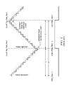
- a high-precision PWM signal 405 is generated by adding a delay time to a leading edge 410 of the low-precision output waveform 420 of the PWM unit 220 and subtracting that same delay time to a falling edge 430 of the low-precision output waveform 420 .
- the added and subtracted delay times are exactly equal (or nearly exactly equal, e.g., exact within a precision requirement of a given system).
- the leading edge 440 of the high-precision PWM waveform 450 is delayed (or pushed out) by a period of T shift 460 that is calculated based on p divisions out of the 2 M partitions of one system clock period
- T shift p 2 M ⁇ T sclk ) ; accordingly, the trailing edge 470 of the high-precision PWM waveform 450 is advanced (i.e., pulled in) also by the period of T shift .
- the high-precision trailing edge 470 of the high-precision PWM waveform 450 occurs earlier in time than the low-precision PWM trailing edge 430 , however, in some embodiments, the high-precision trailing edge 470 may be measured from an earlier edge of the low-precision PWM signal 420 .
- the trailing edge 470 thus happens earlier in time by p divisions out of the 2 M partitions of one system clock period.
- leading edge 440 and trailing edge 470 are shifted (or delayed) by different (but related) amounts of time; the sum of the delay times of the leading and trailing edges is thus equal to one system clock period.
- other methods of creating the high-precision leading 440 and trailing 470 edges are within the scope of the present invention, and the present invention is not limited to only this embodiment.
- the amounts that the high-precision leading 440 and trailing 470 edges may be computed separately and held in different registers.
- the high-precision control unit includes a DLL 510 having a digital delay line 520 that includes a plurality of individual delay units 530 , the delay times of which may vary with the time, process, voltage, temperature, and/or other factors.
- a phase comparator 540 compares the output of the delay line 520 to an input clock 550 .
- a counter 560 that controls a delay of the DLL 510 is varied based on the output of the phase comparator 540 to speed up or slow down the delay times of each delay unit 530 until the DLL 510 is locked to one cycle of the input clock 550 .
- the DLL 510 locks itself to the system clock at startup.
- a digital calibrated code (DLL_Code) may be generated to calibrate the delay time of each individual delay unit 530 using Eq. (1).
- (Calibrated code ⁇ T unit )+ T offset T sclk (1), where T offset includes the additional delay introduced by a multiplexer 570 in the delay line 520 and the calibrated code (DLL_Code) may be stored by the DLL 510 in a digital hardware register 565 .
- the multiplexer 570 may be used to select one of the outputs of at least one of the delay units 530 .
- an offset delay line 580 is incorporated in the DLL 510 to compensate for the additional delay time, i.e., T offset .
- the offset delay line 580 includes a multiplexer 590 comparable to the multiplexer 570 in the delay line 520 and essentially subtracts its non-deterministic delay from the delay line 520 .
- the outputs of the offset delay line 580 and the delay line 520 are fed into the inputs of the phase comparator 540 ; the phase comparator 540 then removes the additional offset delay.
- the DLL 510 allows a continuous self-calibration of the delay units 530 over a period of time thereby eliminating the need for user calibration.
- the high-precision control unit further includes a delay line 610 and control circuitry 620 .
- the delay line 610 is associated with a PWM channel, where the delay line 610 shifts (or delays) the PWM waveform.
- control circuitry 620 may be activated to produce a precise shift (or delay) based on the obtained calibration data (e.g., calibrated code 625 ).
- the precise delay shifts the PWM waveform by the p divisions out of the 2 M partitions of one clock period.
- the control circuitry 620 may perform two operations: a multiplication operation 630 followed by a truncation operation 640 using a multiplier circuit and a truncating circuit, respectively.
- the calibrated code 625 is multiplied by the shift stage number, p, generated from, for example, a control register 650 that includes a binary representation (e.g., a M-bit word stored in a hardware register) of the desired shift stage number.
- the multiplication product may be given as: p ⁇ Calibrated code.
- the last M bits of the multiplication product are then truncated using, for example, a truncating circuit to perform a division and generate a digital delay code 660 that has the same number of bits as that of the calibrated code.
- the digital delay code 660 may be applied to multiple delay units in the delay line 610 associated with the PWM channel to shift the input of the high precision PWM by p divisions out of the 2 M partitions of one system clock period.
- the generated delay may thus be a fraction of the system clock period; this subdivision of the system clock results in an increased resolution of the high precision PWM output.
- the delay code is obtained by continuously calibrating the delay units 530 of the DLL 510 over a period of time, the generated shifted delay is invariant of the time, process, voltage, and/or temperature.
- a DSP typically includes multiple (e.g., between 8 to 16) PWM channels
- employing a high precision PWM in each PWM channel may result in increased area requirements for the implemented chip.
- the length of the delay line (and consequent area) may increase rapidly.
- the calibrated DLL such as the DLL 510
- the multi-stage DLL 710 may serve as a base DLL (a calibrated DLL) that is shared by at least some of the multiple PWM channels to generate a coarse delay time for the PWM waveform in each PWM channel.
- a delay line implemented in each PWM channel for subsequently finely adjusting the delay time for the PWM waveform therein may have less individual delay units; the delay units in the delay line of each PWM channel may be identical to that in the DLL 710 .
- the shared, multi-stage DLL 710 thus reduces the length of the delay line in each PWM channel and significantly minimizes the chip area occupied thereby.
- the present invention is not limited to any particular number of DLL stages; any number that is suitable for splitting the DLL and provides phase shifts up to one clock cycle is within the scope of the present invention.
- the DLL may be split into 8 or 16 stages for a higher number of PWM channels.
- FIG. 8 depicts one embodiment of a complete schematic diagram of the high-precision control unit.
- the high-precision control unit 810 is used in a single PWM channel that includes a multi-stage DLL 820 for generating phase-shifted versions of the system clock.
- the clock phase shifts may be controlled via the first u bits 830 of a control register 840 that provides a binary representation of the desired PWM waveform delay.
- the first two high-order bits of the control register 840 may be fed to a quadrant multiplexer 850 that selects a stage of the multi-stage DLL 820 , and the clock phase shift thereof is applied to generate a coarse delay to the PWM output.
- the multi-stage DLL 820 are then provided to generate a fine delay of the PWM output using a multiplier 860 that multiplies the calibrated code (DLL Code) from multi-stage DLL 820 with the remaining v low-order bits 850 to generate a digital control code (Delay Code), which is applied to a delay line 870 for the PWM channel, containing a shorter delay line in each PWM channel.
- the DLL 820 , the control register 840 , the multiplier 860 and/or the delay line 870 associated with the PWM channel may be integrated on a chip. Because the multi-stage DLL 820 may be shared between multiple PWM channels, the occupied area on the chip may be reduced. In some embodiments, the multi-stage DLL 820 allows continuous calibration of the delays provided by the delay units; the entire high precision control nit 810 may thus act as a self-calibrated high precision PWM channel that requires no external calibrations by the user.
Landscapes
- Pulse Circuits (AREA)
- Stabilization Of Oscillater, Synchronisation, Frequency Synthesizers (AREA)
Abstract
Description
where w2, p and M are integers (1≦p≦2M and 1≦M) and
denotes a delay time that is a fraction of one system clock period. Accordingly, the PWM waveform is shifted by a time, Tshift, that is less than a period of the system clock
and the resolution of the high precision PWM is thereby increased to
accordingly, the trailing
(Calibrated code×T unit)+T offset =T sclk (1),
where Toffset includes the additional delay introduced by a
Calibrated code×T unit =T sclk (2)
The
The
The
Claims (27)
Priority Applications (1)
| Application Number | Priority Date | Filing Date | Title |
|---|---|---|---|
| US13/600,933 US8994426B2 (en) | 2012-08-31 | 2012-08-31 | Method and systems for high-precision pulse-width modulation |
Applications Claiming Priority (1)
| Application Number | Priority Date | Filing Date | Title |
|---|---|---|---|
| US13/600,933 US8994426B2 (en) | 2012-08-31 | 2012-08-31 | Method and systems for high-precision pulse-width modulation |
Publications (2)
| Publication Number | Publication Date |
|---|---|
| US20140062551A1 US20140062551A1 (en) | 2014-03-06 |
| US8994426B2 true US8994426B2 (en) | 2015-03-31 |
Family
ID=50186677
Family Applications (1)
| Application Number | Title | Priority Date | Filing Date |
|---|---|---|---|
| US13/600,933 Active 2032-12-14 US8994426B2 (en) | 2012-08-31 | 2012-08-31 | Method and systems for high-precision pulse-width modulation |
Country Status (1)
| Country | Link |
|---|---|
| US (1) | US8994426B2 (en) |
Cited By (1)
| Publication number | Priority date | Publication date | Assignee | Title |
|---|---|---|---|---|
| US20170040988A1 (en) * | 2015-07-17 | 2017-02-09 | Infineon Technologies Ag | Method and apparatus for providing an adjustable high resolution dead time |
Families Citing this family (20)
| Publication number | Priority date | Publication date | Assignee | Title |
|---|---|---|---|---|
| US9996105B1 (en) * | 2013-03-14 | 2018-06-12 | Marvell Israel (M.I.S.L) Ltd | High precision event timing in network devices |
| CN104980126A (en) * | 2014-04-01 | 2015-10-14 | 中兴通讯股份有限公司 | Clock duty ratio adjusting circuit and multiphase clock generator |
| KR102295058B1 (en) | 2015-08-19 | 2021-08-31 | 삼성전자주식회사 | Semiconductor memory system and semiconductor memory device and operating method for semiconductor memory device |
| EP3362804B1 (en) | 2015-10-14 | 2024-01-17 | WiTricity Corporation | Phase and amplitude detection in wireless energy transfer systems |
| WO2017070009A1 (en) | 2015-10-22 | 2017-04-27 | Witricity Corporation | Dynamic tuning in wireless energy transfer systems |
| KR102055315B1 (en) | 2015-10-29 | 2019-12-13 | 위트리시티 코포레이션 | Controllers for Wireless Power Systems |
| US9832013B2 (en) * | 2016-02-01 | 2017-11-28 | Oracle International Corporation | Phased clock error handling |
| CA3012325A1 (en) | 2016-02-02 | 2017-08-10 | Witricity Corporation | Controlling wireless power transfer systems |
| EP3203634A1 (en) | 2016-02-08 | 2017-08-09 | WiTricity Corporation | Pwm capacitor control |
| US9640244B1 (en) * | 2016-03-29 | 2017-05-02 | Apple Inc. | Pre-calibration for multiple performance states |
| US9998126B1 (en) * | 2017-07-07 | 2018-06-12 | Qualcomm Incorporated | Delay locked loop (DLL) employing pulse to digital converter (PDC) for calibration |
| KR20190036258A (en) * | 2017-09-27 | 2019-04-04 | 에스케이하이닉스 주식회사 | Semiconductor apparatus for detecting edge of signal |
| EP3624318B1 (en) * | 2018-09-12 | 2021-11-17 | ABB Schweiz AG | Transmitting energy and a data signal via a transformer |
| CN111327298B (en) * | 2020-03-12 | 2021-03-30 | 湖南毂梁微电子有限公司 | Ultra-high precision digital pulse signal generation circuit and method |
| CN113948033B (en) * | 2020-07-15 | 2023-01-17 | 厦门凌阳华芯科技股份有限公司 | High-precision PWM driving method, device and medium for LED display screen |
| CN114629476A (en) * | 2020-12-08 | 2022-06-14 | 华大半导体有限公司 | High resolution pulse width modulation signal generating circuit |
| CN113315492B (en) * | 2021-06-03 | 2022-03-29 | 谷芯(广州)技术有限公司 | Low-overhead precision calibration circuit and method for high-precision delay chain |
| CN114978127B (en) * | 2022-06-13 | 2023-04-07 | 湖南毂梁微电子有限公司 | High-precision PWM dead zone control circuit and PWM control system |
| CN116015253B (en) * | 2022-12-13 | 2024-04-09 | 上海极海盈芯科技有限公司 | Self-correcting delay circuit, micro-processing chip and motor control system |
| CN116248085A (en) * | 2022-12-28 | 2023-06-09 | 无锡摩芯半导体有限公司 | Implementation method of high-precision delay generating circuit |
Citations (7)
| Publication number | Priority date | Publication date | Assignee | Title |
|---|---|---|---|---|
| US6137328A (en) * | 1998-05-29 | 2000-10-24 | Hyundai Electronics Industries Co., Ltd. | Clock phase correction circuit |
| US6819190B2 (en) * | 2002-12-10 | 2004-11-16 | Intersil Americas Inc. | Robust fractional clock-based pulse generator for digital pulse width modulator |
| US20050030206A1 (en) * | 2003-08-08 | 2005-02-10 | Li Qiong M. | High-resolution timers and pulse width modulators |
| US7312668B2 (en) * | 2003-06-11 | 2007-12-25 | Koninklijke Philips Electronics N.V. | High resolution PWM generator or digitally controlled oscillator |
| US7439787B2 (en) * | 2006-07-27 | 2008-10-21 | Freescale Semiconductor, Inc. | Methods and apparatus for a digital pulse width modulator using multiple delay locked loops |
| US7528640B2 (en) * | 2006-12-15 | 2009-05-05 | Industrial Technology Research Institute | Digital pulse-width control apparatus |
| US8564345B2 (en) * | 2011-04-01 | 2013-10-22 | Intel Corporation | Digitally controlled delay lines with fine grain and coarse grain delay elements, and methods and systems to adjust in fine grain increments |
-
2012
- 2012-08-31 US US13/600,933 patent/US8994426B2/en active Active
Patent Citations (7)
| Publication number | Priority date | Publication date | Assignee | Title |
|---|---|---|---|---|
| US6137328A (en) * | 1998-05-29 | 2000-10-24 | Hyundai Electronics Industries Co., Ltd. | Clock phase correction circuit |
| US6819190B2 (en) * | 2002-12-10 | 2004-11-16 | Intersil Americas Inc. | Robust fractional clock-based pulse generator for digital pulse width modulator |
| US7312668B2 (en) * | 2003-06-11 | 2007-12-25 | Koninklijke Philips Electronics N.V. | High resolution PWM generator or digitally controlled oscillator |
| US20050030206A1 (en) * | 2003-08-08 | 2005-02-10 | Li Qiong M. | High-resolution timers and pulse width modulators |
| US7439787B2 (en) * | 2006-07-27 | 2008-10-21 | Freescale Semiconductor, Inc. | Methods and apparatus for a digital pulse width modulator using multiple delay locked loops |
| US7528640B2 (en) * | 2006-12-15 | 2009-05-05 | Industrial Technology Research Institute | Digital pulse-width control apparatus |
| US8564345B2 (en) * | 2011-04-01 | 2013-10-22 | Intel Corporation | Digitally controlled delay lines with fine grain and coarse grain delay elements, and methods and systems to adjust in fine grain increments |
Cited By (2)
| Publication number | Priority date | Publication date | Assignee | Title |
|---|---|---|---|---|
| US20170040988A1 (en) * | 2015-07-17 | 2017-02-09 | Infineon Technologies Ag | Method and apparatus for providing an adjustable high resolution dead time |
| US9935623B2 (en) * | 2015-07-17 | 2018-04-03 | Infineon Technologies Ag | Method and apparatus for providing an adjustable high resolution dead time |
Also Published As
| Publication number | Publication date |
|---|---|
| US20140062551A1 (en) | 2014-03-06 |
Similar Documents
| Publication | Publication Date | Title |
|---|---|---|
| US8994426B2 (en) | Method and systems for high-precision pulse-width modulation | |
| US7202719B2 (en) | Method and apparatus for frequency synthesis | |
| US10067478B1 (en) | Use of a recirculating delay line with a time-to-digital converter | |
| US8120401B2 (en) | Methods and systems for digital pulse width modulator | |
| US7459951B2 (en) | Self-calibrating digital pulse-width modulator (DPWM) | |
| US7439787B2 (en) | Methods and apparatus for a digital pulse width modulator using multiple delay locked loops | |
| US20160277030A1 (en) | Frequency synthesizer with dynamic phase and pulse-width control | |
| US11387813B2 (en) | Frequency multiplier and delay-reused duty cycle calibration method thereof | |
| KR20160065632A (en) | Time-to-Digital Converter using a Stochastic Phase Interpolation | |
| US7948274B2 (en) | Frequency generation circuitry and method | |
| US8907704B2 (en) | Frequency synthesizer | |
| US9571071B2 (en) | Frequency synthesizer circuit | |
| US20140118045A1 (en) | Apparatus for controlling duty ratio of signal | |
| US20090051347A1 (en) | High frequency delay circuit and test apparatus | |
| CN104584430B (en) | Phase rotation device based on reference voltage | |
| US8664990B2 (en) | Coherent phase locked loop | |
| WO2013095487A1 (en) | Hybrid digital pulse width modulation (pwm) based on phases of a system clock | |
| US20040027181A1 (en) | Clock multiplying PLL circuit | |
| US20030173945A1 (en) | Method and apparatus for digital frequency conversion | |
| KR100884642B1 (en) | Delayed fixed loop based frequency multiplier and method with self-correction function | |
| KR101013920B1 (en) | Frequency multiplication system and its control method | |
| US20160028350A1 (en) | Modified Flying Adder Architecture | |
| US7995699B2 (en) | DLL circuit with wide-frequency locking range and error-locking-avoiding function | |
| JP3578943B2 (en) | Delay generator and frequency synthesizer and multiplier using the delay generator | |
| KR101609125B1 (en) | Digital delay locked loop circuit and digital pulse width modulation circuit using thereof |
Legal Events
| Date | Code | Title | Description |
|---|---|---|---|
| AS | Assignment |
Owner name: ANALOG DEVICES, INC., MASSACHUSETTS Free format text: ASSIGNMENT OF ASSIGNORS INTEREST;ASSIGNORS:BHAUMIK, WREEJU;GOPALRAO, SENTHIL KUMAR DEVANDAYA;REEL/FRAME:029497/0555 Effective date: 20121128 |
|
| STCF | Information on status: patent grant |
Free format text: PATENTED CASE |
|
| MAFP | Maintenance fee payment |
Free format text: PAYMENT OF MAINTENANCE FEE, 4TH YEAR, LARGE ENTITY (ORIGINAL EVENT CODE: M1551); ENTITY STATUS OF PATENT OWNER: LARGE ENTITY Year of fee payment: 4 |
|
| MAFP | Maintenance fee payment |
Free format text: PAYMENT OF MAINTENANCE FEE, 8TH YEAR, LARGE ENTITY (ORIGINAL EVENT CODE: M1552); ENTITY STATUS OF PATENT OWNER: LARGE ENTITY Year of fee payment: 8 |