US8994023B2 - Thin film transistor array substrate and method of fabricating the same - Google Patents
Thin film transistor array substrate and method of fabricating the same Download PDFInfo
- Publication number
- US8994023B2 US8994023B2 US13/115,088 US201113115088A US8994023B2 US 8994023 B2 US8994023 B2 US 8994023B2 US 201113115088 A US201113115088 A US 201113115088A US 8994023 B2 US8994023 B2 US 8994023B2
- Authority
- US
- United States
- Prior art keywords
- oxide semiconductor
- pattern
- transistor array
- array substrate
- thin film
- Prior art date
- Legal status (The legal status is an assumption and is not a legal conclusion. Google has not performed a legal analysis and makes no representation as to the accuracy of the status listed.)
- Active, expires
Links
Images


Classifications
-
- H—ELECTRICITY
- H01—ELECTRIC ELEMENTS
- H01L—SEMICONDUCTOR DEVICES NOT COVERED BY CLASS H10
- H01L27/00—Devices consisting of a plurality of semiconductor or other solid-state components formed in or on a common substrate
- H01L27/02—Devices consisting of a plurality of semiconductor or other solid-state components formed in or on a common substrate including semiconductor components specially adapted for rectifying, oscillating, amplifying or switching and having at least one potential-jump barrier or surface barrier; including integrated passive circuit elements with at least one potential-jump barrier or surface barrier
- H01L27/12—Devices consisting of a plurality of semiconductor or other solid-state components formed in or on a common substrate including semiconductor components specially adapted for rectifying, oscillating, amplifying or switching and having at least one potential-jump barrier or surface barrier; including integrated passive circuit elements with at least one potential-jump barrier or surface barrier the substrate being other than a semiconductor body, e.g. an insulating body
- H01L27/1214—Devices consisting of a plurality of semiconductor or other solid-state components formed in or on a common substrate including semiconductor components specially adapted for rectifying, oscillating, amplifying or switching and having at least one potential-jump barrier or surface barrier; including integrated passive circuit elements with at least one potential-jump barrier or surface barrier the substrate being other than a semiconductor body, e.g. an insulating body comprising a plurality of TFTs formed on a non-semiconducting substrate, e.g. driving circuits for AMLCDs
- H01L27/1222—Devices consisting of a plurality of semiconductor or other solid-state components formed in or on a common substrate including semiconductor components specially adapted for rectifying, oscillating, amplifying or switching and having at least one potential-jump barrier or surface barrier; including integrated passive circuit elements with at least one potential-jump barrier or surface barrier the substrate being other than a semiconductor body, e.g. an insulating body comprising a plurality of TFTs formed on a non-semiconducting substrate, e.g. driving circuits for AMLCDs with a particular composition, shape or crystalline structure of the active layer
- H01L27/1225—Devices consisting of a plurality of semiconductor or other solid-state components formed in or on a common substrate including semiconductor components specially adapted for rectifying, oscillating, amplifying or switching and having at least one potential-jump barrier or surface barrier; including integrated passive circuit elements with at least one potential-jump barrier or surface barrier the substrate being other than a semiconductor body, e.g. an insulating body comprising a plurality of TFTs formed on a non-semiconducting substrate, e.g. driving circuits for AMLCDs with a particular composition, shape or crystalline structure of the active layer with semiconductor materials not belonging to the group IV of the periodic table, e.g. InGaZnO
-
- H—ELECTRICITY
- H01—ELECTRIC ELEMENTS
- H01L—SEMICONDUCTOR DEVICES NOT COVERED BY CLASS H10
- H01L27/00—Devices consisting of a plurality of semiconductor or other solid-state components formed in or on a common substrate
- H01L27/02—Devices consisting of a plurality of semiconductor or other solid-state components formed in or on a common substrate including semiconductor components specially adapted for rectifying, oscillating, amplifying or switching and having at least one potential-jump barrier or surface barrier; including integrated passive circuit elements with at least one potential-jump barrier or surface barrier
- H01L27/12—Devices consisting of a plurality of semiconductor or other solid-state components formed in or on a common substrate including semiconductor components specially adapted for rectifying, oscillating, amplifying or switching and having at least one potential-jump barrier or surface barrier; including integrated passive circuit elements with at least one potential-jump barrier or surface barrier the substrate being other than a semiconductor body, e.g. an insulating body
- H01L27/1214—Devices consisting of a plurality of semiconductor or other solid-state components formed in or on a common substrate including semiconductor components specially adapted for rectifying, oscillating, amplifying or switching and having at least one potential-jump barrier or surface barrier; including integrated passive circuit elements with at least one potential-jump barrier or surface barrier the substrate being other than a semiconductor body, e.g. an insulating body comprising a plurality of TFTs formed on a non-semiconducting substrate, e.g. driving circuits for AMLCDs
- H01L27/1255—Devices consisting of a plurality of semiconductor or other solid-state components formed in or on a common substrate including semiconductor components specially adapted for rectifying, oscillating, amplifying or switching and having at least one potential-jump barrier or surface barrier; including integrated passive circuit elements with at least one potential-jump barrier or surface barrier the substrate being other than a semiconductor body, e.g. an insulating body comprising a plurality of TFTs formed on a non-semiconducting substrate, e.g. driving circuits for AMLCDs integrated with passive devices, e.g. auxiliary capacitors
Definitions
- Exemplary embodiments of the present invention relate to a thin film transistor array substrate capable of reducing degradation of a device due to degradation of an oxide semiconductor pattern, and a method of fabricating the same.
- a liquid crystal display is one of the most widely-used flat panel displays (FPDs).
- a LCD may include two substrates on which electrodes are formed, and a liquid crystal layer interposed between the substrates. Voltages may be applied to the electrodes to change the orientation of liquid crystal molecules of the liquid crystal layer to control the amount of light transmitted by the LCD.
- a LCD may include thin film transistors (TFTs) for controlling pixels.
- TFTs thin film transistors
- a TFT may include a gate electrode to which a switching signal is applied, a source electrode to which a data voltage is applied, and a drain electrode for outputting the data voltage, thereby forming a switching element having three terminals.
- the TFT may include an active layer formed between the gate electrode and the source electrode, and the gate electrode and the drain electrode.
- the active layer included in the TFT may generally be formed of an amorphous silicon layer. Due to an increasing demand for a high performance device with a large display size, the use of oxide semiconductors in TFTs is being researched.
- a TFT is fabricated using an oxide semiconductor
- degradation of the TFT may occur due to degradation of an oxide semiconductor layer during etching and deposition processes. Therefore, a structure and method capable of reducing the degradation of a TFT due to degradation of the oxide semiconductor layer is needed.
- Exemplary embodiments of the present invention provide a thin film transistor array substrate capable of reducing degradation of a device resulting from degradation of an oxide semiconductor pattern.
- Exemplary embodiments of the present invention also provide a method of fabricating a thin film transistor array substrate capable of reducing degradation of a device resulting from degradation of an oxide semiconductor pattern.
- Exemplary embodiments of the present invention provide a thin film transistor array substrate including a gate electrode, a gate insulating film, an oxide semiconductor pattern, an anti-etching pattern, a source electrode, and a drain electrode.
- the gate electrode is disposed on a substrate.
- the gate insulating film is disposed on the substrate.
- the oxide semiconductor pattern is disposed on the gate insulating film.
- the anti-etching pattern is disposed on the oxide semiconductor pattern.
- the source electrode and the drain electrode are disposed on the anti-etching pattern.
- the oxide semiconductor pattern includes an edge portion, and the edge portion includes a conductive region and a non-conductive region.
- Exemplary embodiments of the present invention also provide a thin film transistor array substrate including a gate electrode, a gate insulating film, an oxide semiconductor pattern, an anti-etching pattern, a passivation film, and a column spacer.
- the gate electrode is disposed on a substrate.
- the gate insulating film is disposed on the substrate.
- the oxide semiconductor pattern is disposed on the gate insulating film.
- the anti-etching pattern is disposed on the oxide semiconductor pattern.
- the passivation film is disposed on the anti-etching pattern.
- the column spacer is formed through the passivation film and the gate insulating film.
- the column spacer includes a first sidewall in contact with the passivation film, the anti-etching pattern, the oxide semiconductor pattern, and the gate insulating film, and a second sidewall in contact with the passivation film and the gate insulating film.
- Exemplary embodiments of the present invention provide an method of fabricating a thin film transistor array substrate including sequentially forming a gate insulating film, an oxide semiconductor layer, and an anti-etching film on a substrate including a gate electrode, forming a preliminary anti-etching pattern by patterning the anti-etching film, and forming, on the oxide semiconductor layer and the preliminary anti-etching pattern, a source electrode and a drain electrode spaced apart from the source electrode.
- the method further includes forming a preliminary oxide semiconductor pattern by patterning the oxide semiconductor layer using the preliminary anti-etching pattern, the source electrode and the drain electrode as a mask, forming a passivation film on the preliminary anti-etching pattern, the source electrode, and the drain electrode, and forming at least one column spacer opening through the passivation film.
- Forming at least one column spacer opening include forming an anti-etching pattern and an oxide semiconductor pattern by etching a portion of the preliminary anti-etching pattern and a region of the preliminary oxide semiconductor pattern overlapping a portion of the preliminary anti-etching pattern.
- FIG. 1A illustrates a layout of a thin film transistor array substrate according to exemplary embodiments of the present invention.
- FIG. 1B is an enlarged view of circle X in FIG. 1A according to exemplary embodiments of the present invention.
- FIG. 2A illustrates cross sectional views taken along lines A-A′ and B-B′ of FIG. 1B according to exemplary embodiments of the present invention.
- FIG. 2B is an enlarged view of circle Y in FIG. 2A according to exemplary embodiments of the present invention.
- FIG. 3 is a cross sectional view taken along line C-C′ of FIG. 1B according to exemplary embodiments of the present invention.
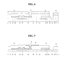
- FIG. 4 , FIG. 5 , FIG. 6 , and FIG. 7 illustrate cross sectional views showing the sequential steps of the method of fabricating a thin film transistor array substrate according to exemplary embodiments of the present invention.
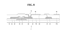
- FIG. 8 illustrates a cross sectional view of a thin film transistor array substrate according to exemplary embodiments of the present invention.
- FIG. 9A illustrates a layout of a thin film transistor array substrate according to exemplary embodiments of the present invention.
- FIG. 9B illustrates cross sectional views taken along lines A-A′ and B-B′ of FIG. 9A according to exemplary embodiments of the present invention.
- FIG. 10A illustrates a layout of a thin film transistor array substrate according to exemplary embodiments of the present invention
- FIG. 10B is an enlarged view of circle Y in FIG. 10A according to exemplary embodiments of the present invention.
- FIG. 11 illustrates a layout of a thin film transistor array substrate according to exemplary embodiments of the present invention.
- FIG. 12A illustrates a layout of a thin film transistor array substrate according to exemplary embodiments of the present invention.
- FIG. 12B is an enlarged view of circle Z in FIG. 12A according to exemplary embodiments of the present invention.
- FIG. 12C is a cross sectional view taken along line C-C′ of FIG. 12B according to exemplary embodiments of the present invention.
- FIG. 1A illustrates a layout of the thin film transistor array substrate according to exemplary embodiments of the present invention.
- FIG. 1B is an enlarged view of circle X in FIG. 1A .
- FIG. 2A illustrates cross sectional views taken along lines A-A′ and B-B′ of FIG. 1B .
- FIG. 2B is an enlarged view of circle Y in FIG. 2A .
- FIG. 3 is a cross sectional view taken along line C-C′ of FIG. 1B .
- gate wirings 22 and 24 may transmit a gate signal and may be formed on an insulating substrate 10 .
- the insulating substrate 10 may be formed of any suitable material including, for example, glass such as soda lime glass and borosilicate glass or plastic.
- the gate wirings 22 and 24 may include a gate line 22 extending in a horizontal direction, and a gate electrode 24 of a thin film transistor.
- the gate electrode 24 may be connected to the gate line 22 and formed in a protruded shape.
- the gate electrode 24 may include a gate electrode opening 26 .
- a column spacer 94 may be arranged in the gate electrode opening 26 as shall be described in further detail below.
- Storage wirings 28 and 29 may supply a storage voltage and may be formed on the insulating substrate 10 .
- Storage wirings 28 and 29 may include a storage line 28 formed across a pixel region, and a storage electrode 29 branched from the storage line 28 .
- the storage line 28 may extend in parallel to the gate line 22 and the storage electrode 29 may extend in parallel to a data line 62 .
- the storage electrode 29 may be formed in a rectangular ring shape along the data line 62 (see FIG. 1A ). For example, an opening region may be formed in a central portion of the storage electrode 29 such that the data line 62 is positioned in the opening region. A ring portion of the storage electrode 29 may at least partially overlap a pixel electrode 80 , thereby forming a storage capacitor to improve the charge storage capacity of a pixel. Further, the storage electrode 29 may serve as a blocking electrode capable of preventing coupling between the pixel electrode 80 and the data line 62 .
- the shape and arrangement of the storage electrode 29 and the storage line 28 are not limited to those illustrated in the drawings and may be modified in various ways. For example, if the storage capacitance generated by overlapping of the pixel electrode 80 and the gate line 22 is sufficient, the storage electrode 29 and the storage line 28 may not be formed.
- a gate insulating film 30 may be formed on the insulating substrate 10 and the gate wirings 22 and 24 .
- the gate insulating film 30 may be formed of any suitable material including, for example, silicon oxide (SiOx), silicon nitride (SiNx), silicon oxynitride (SiON) or the like, but it is not limited thereto.
- An oxide semiconductor pattern 42 may be formed on the gate insulating film 30 .
- the oxide semiconductor pattern 42 may form a channel region of the thin film transistor.
- the channel region may be formed as a result of the oxide semiconductor pattern 42 overlapping the gate electrode.
- the oxide semiconductor pattern 42 may be formed to overlap with the data line 62 and an anti-etching pattern 52 , which will be described in further detail below.
- a sidewall of the anti-etching pattern 52 may be arranged vertically with a sidewall of a passivation film 70 and a sidewall of the oxide semiconductor pattern 42 .
- the sidewalls of the passivation film 70 , the anti-etching pattern 52 , and the oxide semiconductor pattern 42 may be arranged vertically along one sidewall of column spacers 92 and 94 , which will be described in further detail below.
- a portion of the oxide semiconductor pattern 42 may be formed inward from the anti-etching pattern 52 .
- a sidewall of the oxide semiconductor pattern 42 may be formed at a distance D from a sidewall of the anti-etching pattern 52 .
- a sidewall of the anti-etching pattern 52 may protrude from a sidewall of the oxide semiconductor pattern 42 by the distance D.
- the passivation film 70 may be formed below the protruded portion of the anti-etching pattern 52 , in some cases, an empty space may exist below the protruded portion of the anti-etching pattern 52 due to an under-cut. The under-cut may occur below the anti-etching pattern 52 if the oxide semiconductor pattern 42 is formed by wet etching.
- the oxide semiconductor pattern 42 may contain any suitable material including, for example, a compound having a chemical formula of AxBxOx or AxBxCxOx, wherein x is greater than zero; A, B, and C are different; and O is oxygen.
- A may be Zinc (Zn) or Cadmium (Cd);
- B may be Gallium (Ga), Tin (Sn), or Indium (In);
- C may be Zn, Cd, Ga, In, Tantalum (Ta) or Hafnium (Hf).
- the oxide semiconductor pattern 42 may include at least one of InZnO, InGaO, InSnO, ZnSnO, GaSnO, GaZnO, GaZnSnO, GaInZnO, HfInZnO, TaInSnO, ZnO, and any combination thereof.
- Such oxide semiconductors have excellent semiconductor characteristics including the effective mobility of charges that is about 2 to 100 times as high as that of hydrogenated amorphous silicon.
- the oxide semiconductor pattern 42 may have an amorphous phase, a crystalline phase, or a mixed phase of the amorphous and crystalline phases.
- the oxide semiconductor pattern 42 may include edge portions 42 Ec and 42 En positioned between a source electrode 65 and a drain electrode 66 .
- the edge portions 42 Ec and 42 En may include at least one conductive region 42 Ec and at least one non-conductive region 42 En.
- the edge portions 42 Ec and 42 En may be regions positioned between the source electrode 65 and the drain electrode 66 , and positioned along the sidewall of the oxide semiconductor pattern 42 .
- a region from an edge of the oxide semiconductor pattern 42 to a virtual edge line EL defined along the edge of the oxide semiconductor pattern 42 may be defined as the edge portions 42 Ec and 42 En of the oxide semiconductor pattern 42 .
- the edge portions of the oxide semiconductor pattern 42 may include at least one non-conductive region 42 En and at least one conductive region 42 Ec.
- the thin film transistor array substrate 1 may be configured to have a conductive region 42 Ec adjacent to the source electrode 65 , a conductive region 42 Ec adjacent to the drain electrode 66 , and a non-conductive region 42 En between the two conductive regions 42 Ec. This configuration is the same in upper and lower portions of the edge portion with respect to the source electrode 65 and the drain electrode 66 .
- the oxide semiconductor pattern 42 may include the edge portion of the conductive region 42 Ec (in a third region III) between the source and drain electrodes 65 and 66 and the column spacers 92 and 94 .
- the oxide semiconductor pattern 42 may include the edge portion of the non-conductive region 42 En (in a fourth region IV) adjacent to the column spacers 92 and 94 .
- An edge portion of a preliminary oxide semiconductor pattern 42 a (see FIG. 5 ), which will be described in further detail below, may have conductivity due to damage in a process of forming a passivation film 70 .
- hatched areas in column spacer openings 93 and 95 which are openings for forming the column spacers 92 and 94 , may be areas wherein a preliminary anti-etching pattern 52 a and the preliminary oxide semiconductor pattern 42 a overlap with the column spacer openings 93 and 95 .
- a conductive portion in the edge portion of the preliminary oxide semiconductor pattern 42 a may overlap with the hatched areas.
- the hatched areas may be removed in a process of forming the column spacer openings 93 and 95 .
- the oxide semiconductor pattern 42 of the fourth region IV adjacent to the column spacers 92 and 94 may include the edge portion of the non-conductive region 42 En.
- At least a portion of the edge portion of the oxide semiconductor pattern 42 which is not in contact with the column spacers 92 and 94 , may be the conductive region 42 Ec, and at least a portion of the edge portion of the oxide semiconductor pattern 42 , which is in contact with or adjacent to the column spacers 92 and 94 , may be the non-conductive region 42 En.
- the source electrode 65 may not be electrically connected to the drain electrode 66 along the edge portion of the oxide semiconductor pattern 42 , even though a residual region of the edge portion of the oxide semiconductor pattern 42 may be a conductive region 42 Ec.
- the anti-etching pattern 52 may be formed on the oxide semiconductor pattern 42 .
- the thin film transistor array substrate 1 may include a first region I in which the anti-etching pattern 52 overlaps with the gate electrode 24 and a second region II in which the anti-etching pattern 52 does not overlap with the gate electrode 24 .
- the second region II may be formed of one or more second regions, and at least one of the second regions may be formed in the gate electrode opening 26 . As shown in FIG. 1A and FIG. 1B , the second region II may correspond to a portion of the anti-etching pattern 52 protruding from the end of the gate electrode 24 which extends from the gate line 22 and a portion of the anti-etching pattern 52 extending to the inside of the gate electrode opening 26 .
- the anti-etching pattern 52 may have any suitable dimension and/or shape.
- the anti-etching pattern 52 may have a first width W 1 and a second width W 2 smaller than the first width W 1 , and may be formed in a T shape.
- the anti-etching pattern 52 of the second region II arranged in the gate electrode opening 26 may have the second width W 2 and the anti-etching pattern 52 arranged outside the gate electrode opening 26 may have the first width W 1 .
- the sidewall of the anti-etching pattern 52 of the second region II may be arranged vertically with the sidewall of the oxide semiconductor pattern 42 .
- the hatched areas shown in FIG. 1B may be the partial regions of the preliminary oxide semiconductor pattern 42 a and the preliminary anti-etching pattern 52 a which are removed in an etching process for forming the column spacer openings 93 and 95 .
- the portions of the preliminary oxide semiconductor pattern 42 a and the anti-etching pattern 52 a overlapping with regions defined as the column spacer openings 93 and 95 are removed in the etching process, so that the sidewall of the anti-etching pattern 52 and the is sidewall of the oxide semiconductor pattern 42 can be arranged vertically.
- a portion of the sidewall of the anti-etching pattern 52 of the first region I may protrude from the sidewall of the oxide semiconductor pattern 42 .
- a sidewall of the preliminary anti-etching pattern 52 a may protrude from a sidewall of the preliminary oxide semiconductor pattern 42 a by a predetermined distance D due to an etching process of an oxide semiconductor layer that will be described in further detail below.
- the anti-etching pattern 52 of the first region I may not include a region overlapping with the column spacer openings 93 and 95 unlike the second region II. Accordingly, even after the etching process of the oxide semiconductor layer, the sidewall of the anti-etching pattern 52 of the first region I may be maintained to protrude from the sidewall of the oxide semiconductor pattern 42 .
- the anti-etching pattern 52 may include any material selected from the group consisting of SiOx and SiNx, where Si is silicon, N is nitrogen, and x is a number greater than 0.
- the oxide semiconductor pattern 42 may be patterned in a shape substantially identical to a data wiring 62 , 65 , and 66 except in the channel region of the thin film transistor since the oxide semiconductor pattern 42 and the data wiring 62 , 65 and 66 may be patterned using a single etching mask.
- the data wiring 62 , 65 , and 66 may be formed on the gate insulating film 30 , the oxide semiconductor pattern 42 , and the anti-etching pattern 52 .
- the data wiring 62 , 65 , and 66 may include the data line 62 formed vertically to intersect the gate line 22 , thereby defining a pixel.
- the data wiring 62 , 65 , and 66 may also include the source electrode 65 branched off from the data line 62 to extend to an upper portion of the oxide semiconductor pattern 42 , and a drain electrode 66 separated from the source electrode 65 and formed on the oxide semiconductor pattern 42 and the anti-etching pattern 52 to face the source electrode 65 around the gate electrode 24 or the channel region of the thin film transistor.
- the oxide semiconductor pattern 42 may be arranged below the anti-etching pattern 52 , the source electrode 65 , and the drain electrode 66 .
- the data wiring 62 , 65 , and 66 may be directly in contact with the oxide semiconductor pattern 42 and may be formed of a material forming an Ohmic contact. If the data wiring 62 , 65 , and 66 is formed of a material having a work function smaller than that of a material of the oxide semiconductor pattern 42 , an Ohmic contact may be formed between the data wiring 62 , 65 , and 66 and the oxide semiconductor pattern 42 .
- the passivation film 70 may be formed on the data wiring 62 , 65 , and 66 and the anti-etching pattern 52 .
- the passivation film 70 may be formed of any suitable material including, for example, silicon oxide (SiOx), silicon nitride (SiNx), silicon oxynitride (SiON) or the like, but it is not limited thereto.
- the contact hole 75 and the column spacers 92 and 94 may be formed in the passivation film 70 .
- the contact hole 75 may be formed to pass through the passivation film 70 , and the drain electrode 66 may be electrically connected to the pixel electrode 80 via the contact hole 75 .
- the pixel electrode 80 may be formed of any suitable material including, for example, a transparent conductor such as indium tin oxide (ITO) or indium zinc oxide (IZO) or a reflective conductor such as aluminum, but the pixel electrode 80 is not limited thereto.
- the column spacers 92 and 94 may be formed through the passivation film 70 and the gate insulating film 30 .
- Each of the column spacers 92 and 94 may include first and second sidewalls.
- the first sidewalls of the column spacers 92 and 94 may be in contact with the anti-etching pattern 52 , the oxide semiconductor pattern 42 , and the gate insulating film 30
- the second sidewalls may be in contact with the passivation film 70 and the gate insulating film 30 .
- Sidewalls of the passivation film 70 , the anti-etching pattern 52 , and the gate insulating film 30 may be arranged vertically along sidewalls of the column spacers 92 and 94 .
- each of the column spacers 92 and 94 may include upper and lower regions.
- the upper regions of the column spacers 92 and 94 may be formed to have a larger distance between the first and second sidewalls than the distance between the first and second sidewalls in the lower regions of the column spacers 92 and 94 .
- the first sidewalls of the upper regions of the column spacers 92 and 94 may be in contact with the passivation film 70 , the anti-etching pattern, 52 and the oxide semiconductor pattern 42
- the first sidewalls of the lower regions of the column spacers 92 and 94 may be in contact with the gate insulating film 30 .
- the second sidewalls of the upper regions of the column spacers 92 and 94 may be in contact with the passivation film 70 , and the second sidewalls of the lower regions of the column spacers 92 and 94 may be contact with the gate insulating film 30 .
- the upper regions of the column spacers 92 and 94 (and the upper regions of the column spacer openings 93 and 95 ) may not overlap with the gate electrode 24 .
- the column spacers 92 and 94 may overlap with a portion of the passivation film 70 .
- the column spacers 92 and 94 may overlap with at least a portion of the passivation film 70 formed in the second region II.
- the column spacers 92 and 94 may overlap the column spacer openings 93 and 95 formed in the passivation film 70 and the gate insulating film 30 , and extend to the upper surface of the passivation film 70 .
- column spacers 92 and 94 may be formed to include the column spacer openings 93 and 95 (indicated by dotted lines). Accordingly, the column spacers 92 and 94 may overlap with a portion of the passivation film 70 defined as the column spacer openings 93 and 95 .
- the column spacers 92 and 94 may be formed of one or more column spacers. At least one of the column spacers may be formed in the gate electrode opening 26 . As shown in FIG. 1A and FIG. 1B , the column spacers 92 and 94 may include the column spacer 92 , which is in contact with a portion of the anti-etching pattern 52 protruding from the end of the gate electrode 24 extending from the gate line 22 , and the column spacer 94 , which is in contact with a portion of the anti-etching pattern 52 extending to the inside of the gate electrode opening 26 .
- the column spacers 92 and 94 may be formed of any suitable material including, for example, a transparent organic material or a light blocking material.
- FIG. 1A , FIG. 1B , FIG. 2A , FIG. 2B , FIG. 3 , FIG. 4 , FIG. 5 , FIG. 6 , and FIG. 7 illustrate cross sectional views showing the sequential steps of a method to fabricate the thin film transistor array substrate 1 in accordance with exemplary embodiments of the present invention.
- a gate electrode 24 may be formed on the insulating substrate 10 .
- the gate insulating film 30 , the oxide semiconductor layer 40 , and an anti-etching film may be sequentially deposited on the insulating substrate 10 with the gate electrode 24 formed thereon.
- the anti-etching film may be patterned to form the preliminary anti-etching pattern 52 a.
- the gate line 22 , the storage line 28 , and the storage electrode 29 may be formed at the same time as the gate electrode 24 by using the same mask process.
- the insulating substrate 10 may be formed of any various suitable materials including, for example, glass such as soda lime glass and borosilicate glass or plastic.
- a conductive film for gate lines may be formed on the insulating substrate 10 by using a sputtering method. If the insulating substrate 10 is a soda lime glass having a low heat resistance, a low temperature sputtering method may be used. In general, any suitable technique may be used to form the gate wiring 22 and 24 .
- the conductive film for gate lines may be patterned by wet etching or dry etching to form the gate wirings 22 and 24 .
- wet etching an etching solution such as, for example, phosphoric acid, nitric acid, and acetic acid, may be used.
- dry etching a chlorine-based etching gas such as, for example, chlorine (Cl 2 ) and Boron Trichloride (BCl 3 ), may be used.
- the gate line 22 may be formed such that the gate electrode 24 includes the gate electrode opening 26 formed through the gate electrode 24 .
- the gate insulating film 30 may be formed on the insulating substrate 10 and the gate wirings 22 and 24 using any suitable method including, for example, plasma enhanced chemical vapor deposition (PECVD), reactive sputtering, or the like.
- PECVD plasma enhanced chemical vapor deposition
- the gate insulating film 30 may be formed on at least part of or, in some cases, the entire surface of the insulating substrate 10 .
- An oxide semiconductor material may be formed on the gate insulating film 30 by using any suitable method including, for example, a sputtering method, thereby resulting in formation of the oxide semiconductor layer 40 .
- the anti-etching film may be formed on at least part of or, in some cases, the entire surface of the oxide semiconductor layer 40 by using any suitable method including, for example, chemical vapor deposition (CVD).
- the anti-etching film may be made of any suitable material including, for example, a silicon oxide film or silicon nitride film, but is not limited thereto. Further, the anti-etching film may be patterned using any suitable method including, for example, dry etching, to form the preliminary anti-etching pattern 52 a.
- the source electrode 65 and the drain electrode 66 may be formed on the oxide semiconductor layer 40 and the preliminary anti-etching pattern 52 a .
- the oxide semiconductor layer 40 may be patterned by using the preliminary anti-etching pattern 52 a , the source electrode 65 , and the drain electrode 66 as a mask to form the preliminary oxide semiconductor pattern 42 a.
- a conductive layer for data wiring may be formed on the oxide semiconductor layer 40 and the preliminary anti-etching pattern 52 a .
- the conductive layer for data wiring and the oxide semiconductor layer 40 may be etched simultaneously or sequentially using, for example, wet etching to form the data wiring 62 , 65 , and 66 and the preliminary oxide semiconductor pattern 42 a .
- the oxide semiconductor layer 40 may be patterned by using the preliminary anti-etching pattern 52 a , the source electrode 65 , and the drain electrode 66 as a mask.
- a portion of the oxide semiconductor pattern 42 may be formed inward from the anti-etching pattern 52 .
- a sidewall of the oxide semiconductor pattern 42 may be formed at a predetermined distance D from a sidewall of the anti-etching pattern 52 , and the sidewall of the anti-etching pattern 52 may protrude by the predetermined distance D from a sidewall of the oxide semiconductor pattern 42 , as shown in FIG. 2B .
- the source electrode 65 and the drain electrode 66 may be formed on both sides of the gate electrode 24 and may be separate from each other.
- the anti-etching pattern 52 may be exposed in the region where the source electrode 65 is separated from the drain electrode 66 .
- the passivation film 70 may be formed on the preliminary anti-etching pattern 52 a , the source electrode 65 , and the drain electrode 66 . At least a portion of the preliminary anti-etching pattern 52 a of the second region II (see FIG. 3 ) may be etched to form the anti-etching pattern 52 .
- the passivation film 70 may be formed by using any suitable method including, for example, PECVD or reactive sputtering. Further, the passivation film 70 may be any suitable material including, for example, a silicon oxide film or silicon nitride film.
- the edge portion of the preliminary oxide semiconductor pattern 42 a (i.e., the region of the preliminary oxide semiconductor pattern 42 a that is in contact with the passivation film 70 ) may be exposed to a plasma gas or the like during a process of depositing the passivation film 70 .
- the preliminary anti-etching pattern 52 a may be disposed on the preliminary oxide semiconductor pattern 42 a to protect the upper surface of the preliminary oxide semiconductor pattern 42 a from being exposed to the plasma gas or the like.
- the lower surface of the preliminary oxide semiconductor pattern 42 a can be protected by the gate insulating film 30 .
- the preliminary oxide semiconductor pattern 42 a and a sidewall of the preliminary oxide semiconductor pattern 42 a arranged with respect to the data wiring 62 , 65 , and 66 may be exposed to the plasma gas or the like. Accordingly, the edge portion of the preliminary oxide semiconductor pattern 42 a , particularly, the region exposed to the passivation film 70 , may be damaged during the deposition process to provide conductivity.
- a mask pattern 200 for forming the column spacer openings 93 and 95 may be formed on the passivation film 70 , and the passivation film 70 may be patterned by using the mask pattern 200 as a mask.
- a photolithography process may be used to form the column spacer openings 93 and 95 , and a contact hole 75 exposing a portion of the drain electrode 66 .
- the first region I may include the preliminary anti-etching pattern 52 a overlapping with the gate electrode 24 .
- the preliminary anti-etching pattern 52 a does not overlap the gate electrode 24 in the second region II.
- a region of the passivation film 70 overlapping with at least a portion (portion indicated by a dotted line) of the preliminary anti-etching pattern 52 a of the second region II and at least a portion (portion indicated by a dotted line) of the preliminary anti-etching pattern 52 a may be etched simultaneously or sequentially to form the anti-etching pattern 52 .
- the at least a portion (portion indicated by a dotted line) of the preliminary anti-etching pattern 52 a of the second region II may be etched earlier than the preliminary oxide semiconductor pattern 42 a .
- a portion of the preliminary anti-etching pattern 52 a having an etching selectivity similar to that of the passivation film 70 may be removed at the same time.
- the passivation film 70 and the preliminary anti-etching pattern 52 a may be removed at the same time. If the preliminary anti-etching pattern 52 a and the passivation film 70 are formed of different materials, the passivation film 70 and the preliminary anti-etching pattern 52 a may be removed sequentially by using the mask pattern 200 .
- the mask pattern 200 formed on the passivation film 70 may be defined such that the column spacer opening 93 overlaps with portions of the preliminary anti-etching pattern 52 a and the preliminary oxide semiconductor pattern 42 a .
- the mask pattern 200 may expose an overlapping region of the column spacer opening 93 and at least a portion of the edge portion of the preliminary oxide semiconductor pattern 42 a having conductivity, which belongs to the second region II.
- a portion of the edge portion of the oxide semiconductor pattern 42 may be nonconductive. Accordingly, it may be possible to prevent the source electrode 65 from being electrically connected to the drain electrode 66 along the edge portion of the oxide semiconductor pattern 42 .
- the passivation film 70 and the gate insulating film 30 may be removed simultaneously or sequentially.
- the preliminary oxide semiconductor pattern 42 a protruding from the anti-etching pattern 52 may serve as an etching mask.
- a sidewall of the lower region of each of the column spacer openings 93 and 95 that is in contact with the gate insulating film 30 may be defined, at least in part, by a sidewall of the preliminary oxide semiconductor pattern 42 a .
- at least one of the column spacer openings 93 and 95 may include an upper region having a first width and a lower region having a second width smaller than the first width.
- the gate insulating film 30 may be etched such that a sidewall of the lower region of each of the column spacer openings 93 and 95 is arranged vertically with the preliminary oxide semiconductor pattern 42 a.
- the preliminary oxide semiconductor pattern 42 a may have an etching selectivity different from that of the passivation film 70 , the preliminary anti-etching pattern 52 a , and the gate insulating film 30 . Accordingly, the preliminary oxide semiconductor pattern 42 a may be maintained to protrude from the anti-etching pattern 52 .
- the oxide semiconductor pattern 42 may be formed by etching a region of the preliminary oxide semiconductor pattern 42 a overlapping with at least a portion (portion indicated by a dotted line in FIG. 6 ) of the preliminary anti-etching pattern 52 a of the second region II.
- a conductive film for a pixel electrode that is partially connected to the data wiring 62 , 65 , and 66 may be formed on the passivation film 70 .
- the conductive film for a pixel electrode may be any suitable material including, for example, a transparent conductor such as indium tin oxide (ITO) or indium zinc oxide (IZO) or a reflective conductor such as aluminum.
- the conductive film for a pixel electrode may be connected to the drain electrode 66 via the contact hole 75 .
- the pixel electrode 80 may be formed by etching the conductive film for a pixel electrode.
- the oxide semiconductor pattern 42 may be formed by etching a portion of the preliminary oxide semiconductor pattern 42 a protruding from the anti-etching pattern 52 by using the mask pattern used for forming the pixel electrode 80 .
- the conductive film for a pixel electrode 80 and the preliminary oxide semiconductor pattern 42 a may be removed at the same time.
- the conductive film for a pixel electrode 80 and the preliminary oxide semiconductor pattern 42 a may be etched sequentially.
- the column spacer openings 93 and 95 including upper and lower regions having different widths may be formed.
- forming at least one of the column spacer openings 93 and 95 may include forming the anti-etching pattern 52 and the oxide semiconductor pattern 42 by etching a portion of the preliminary anti-etching pattern 52 a and a region of the preliminary oxide semiconductor pattern 42 a overlapping a portion of the preliminary anti-etching pattern 52 a.
- At least one of the column spacers 92 and 94 may be formed by burying a material in at least one of the column spacer openings 93 and 95 .
- the material of the column spacers 92 and 94 may be any suitable material including, for example, a transparent organic material or a light blocking material.
- a bottom gate structure in which a gate electrode 24 is disposed below an oxide semiconductor layer 42 has been described, exemplary embodiments of the present invention are not limited thereto, and a top gate structure in which a gate electrode is disposed on an oxide semiconductor layer may similarly be implemented to reduce the degradation of a TFT due to the degradation of the oxide semiconductor layer.
- FIG. 8 illustrates a cross sectional view of a thin film transistor array substrate 2 .
- the thin film transistor array substrate 2 is different from the thin film transistor array substrate 1 described hereinabove in that the thin film transistor array substrate 2 has a color filter on array (COA) structure in which color filters 71 R and 71 G are formed in place of the passivation film 70 (see FIG. 2A ).
- COA color filter on array
- the same or substantially the same components as those of the thin film transistor array substrate 1 described hereinabove are designated by the same reference numerals, and a detailed description thereof will be omitted.
- the color filters 71 R and 71 G or an organic film may be formed in place of a passivation film.
- the color filters 71 R and 71 G or organic film may be formed on the gate insulating film 30 , the anti-etching pattern 52 , the source electrode 65 , and the drain electrode 66 , the source electrode 65 may still be prevented from being electrically connected to the drain electrode 66 along the edge portion of the oxide semiconductor pattern 42 .
- FIG. 9A illustrates a layout of the thin film transistor array substrate 3
- FIG. 9B is a cross sectional view taken along lines A-A′ and B-B′ of FIG. 9A .
- the thin film transistor array substrate 3 is different from the thin film transistor array substrate 1 described hereinabove in that an insulating film 72 may be used in place of the column spacer and may be buried in column spacer openings 93 and 97 .
- the same or substantially the same components as those of the thin film transistor array substrate 1 described hereinabove are designated by the same reference numerals, and a detailed description thereof will be omitted.
- Reference numerals 93 and 97 denote column spacer “openings” because column spacers are not buried therein.
- an edge portion of the oxide semiconductor pattern 42 may include the conductive region 42 Ec and the non-conductive region 42 En. Since the edge portion including the conductive region 42 Ec and the non-conductive region 42 En have been described previously, a repeated description thereof will be omitted.
- the openings 93 and 97 may be filled with an insulating film 72 .
- the passivation film 70 and the insulating film 72 are illustrated as different layers in the FIG. 9B , exemplary embodiments of the invention are not limited thereto.
- the passivation film 70 and the insulating film 72 may be combined into a single layer.
- the passivation film 70 and the insulating film 72 may be formed of the same material thereby providing a single layer of film.
- various modifications and combinations of the passivation film 70 and insulating film 72 may be used.
- FIG. 10A illustrates a layout of the thin film transistor array substrate 4
- FIG. 10B is an enlarged view of circle Y in FIG. 10A .
- the thin film transistor array substrate 4 is different from the thin film transistor array substrate 1 described hereinabove in that an anti etching pattern 54 may have a crisscross (+) pattern.
- an anti etching pattern 54 may have a crisscross (+) pattern.
- the same or substantially the same components as those of the thin film transistor array substrate 1 described hereinabove are designated by the same reference numerals, and a detailed description thereof will be omitted.
- an anti etching pattern 54 of a first region I may have a first width W 1 and the anti etching pattern 54 of a second region II may have a second width W 2 and a third width W 3 .
- the first width W 1 may be larger than the second width W 2 and the third width W 3 .
- the third width W 3 of the anti etching pattern 54 in the second region II which protrudes from an end of the gate electrode 24 extending from a gate line 22 , may be smaller than the first width W 1 of the anti etching pattern 54 in the first region I. Accordingly, the area occupied by column spacers 94 and 96 may be reduced. Thus, if the column spacers 94 and 96 are formed of a light blocking material, an opening ratio can be improved, which is advantageous.
- a method of fabricating the thin film transistor array substrate 4 may be substantially the same as the method of fabricating the thin film transistor array substrate 1 described hereinabove except that the preliminary anti-etching pattern 52 a is formed by patterning the anti-etching film 54 .
- regions defined by the column spacer openings 97 and 95 may overlap with regions of a preliminary oxide semiconductor pattern and a preliminary anti-etching pattern, and patterns in the overlapping regions may be removed by forming the column spacer openings 97 and 95 .
- an edge portion of an oxide semiconductor pattern 44 may include a conductive region 44 Ec and a non-conductive region 44 En.
- patterning of the anti-etching film of the thin film transistor array substrate 4 may be different from the patterning of the anti-etching film of the thin film transistor array substrate 1 in that a shape of the mask pattern may be a crisscross pattern.
- FIG. 11 illustrates a layout of the thin film transistor array substrate 5 .
- the thin film transistor array substrate 5 is different from the thin film transistor array substrate 1 described hereinabove in that the column spacer 92 is buried in at least one of the column spacer openings 93 and 97 .
- an insulating material instead of the column spacer 92 , may be buried in at least one or more column spacer openings 93 and 97 .
- any one of the column spacer openings 93 and 97 may be filled with the column spacer 92
- the other one of the column spacer openings 93 and 97 may be filled with an insulating material, instead of the column spacer 92 .
- the thin film transistor array substrate 5 may include two column spacer openings 93 and 97 .
- One column spacer opening 93 may be filled with the column spacer 92 .
- two column spacer openings 93 and 97 are illustrated in FIG. 11 , two or more column spacer openings may be formed and the column spacer 92 may be partially buried in the two or more column spacer openings 93 and 97 .
- being “partially buried” may refer to the column spacer 92 being buried in some openings of the column spacer openings 93 and 97 .
- the other openings may be filled with an insulating material as noted above.
- the anti-etching pattern 56 may be formed to have a single width without variation in width.
- the anti-etching pattern 56 may be formed in a rectangular shape.
- FIG. 12A illustrates a layout of the thin film transistor array substrate 6 .
- FIG. 12B is an enlarged view of circle Z in FIG. 12A .
- FIG. 12C is a cross sectional view taken along line C-C′ of FIG. 12B .
- the thin film transistor array substrate 6 is different from the thin film transistor array substrates 1 described hereinabove in that no opening is formed in the gate electrode 24 .
- the thin film transistor array substrate 6 may include a gate electrode 24 , and the column spacer openings 93 and 95 may not be formed in the gate electrode 24 .
- the column spacer openings 93 and 95 may be formed in contact with the sidewalls of the anti-etching pattern 52 and the oxide semiconductor pattern 42 .
- the column spacer opening 95 may be formed to pass through the anti-etching pattern 52 and the oxide semiconductor pattern 42 , without passing through the gate electrode 24 . In some cases, however, the column spacer opening 95 may pass through the gate insulating film 30 .
- the gate insulating film 30 corresponding to the column spacer opening 95 may remain by using, for example, a slit mask or the like. Accordingly, the gate electrode 24 may be disposed below the gate insulating film 30 , thereby preventing the gate electrode 24 from being exposed directly.
- At least one of the column spacer openings 93 and 95 of the thin film transistor array substrate 6 may be filled with an insulating material instead of the column spacer 94 , as noted above.
- the column spacer openings 93 and 95 may be filled with the column spacer 92 or an insulating material.
Abstract
Description
Claims (15)
Applications Claiming Priority (2)
| Application Number | Priority Date | Filing Date | Title |
|---|---|---|---|
| KR10-2010-0077300 | 2010-08-11 | ||
| KR1020100077300A KR101701212B1 (en) | 2010-08-11 | 2010-08-11 | Thin film transistor array substrate and method of fabricating the same |
Publications (2)
| Publication Number | Publication Date |
|---|---|
| US20120037906A1 US20120037906A1 (en) | 2012-02-16 |
| US8994023B2 true US8994023B2 (en) | 2015-03-31 |
Family
ID=45564158
Family Applications (1)
| Application Number | Title | Priority Date | Filing Date |
|---|---|---|---|
| US13/115,088 Active 2033-04-12 US8994023B2 (en) | 2010-08-11 | 2011-05-24 | Thin film transistor array substrate and method of fabricating the same |
Country Status (4)
| Country | Link |
|---|---|
| US (1) | US8994023B2 (en) |
| JP (1) | JP5746586B2 (en) |
| KR (1) | KR101701212B1 (en) |
| CN (1) | CN102376721B (en) |
Families Citing this family (4)
| Publication number | Priority date | Publication date | Assignee | Title |
|---|---|---|---|---|
| JP5863399B2 (en) * | 2011-11-07 | 2016-02-16 | 三菱電機株式会社 | Wiring structure, thin film transistor array substrate including the same, and display device |
| JP6306278B2 (en) * | 2012-04-09 | 2018-04-04 | Jsr株式会社 | Semiconductor element, semiconductor substrate, radiation-sensitive resin composition, protective film, and display element |
| KR20150054040A (en) | 2013-11-08 | 2015-05-20 | 삼성디스플레이 주식회사 | Thin film transistor substrate and organic light emitting display apparatus having the same |
| TWI552322B (en) * | 2015-08-06 | 2016-10-01 | 友達光電股份有限公司 | Pixel structure |
Citations (11)
| Publication number | Priority date | Publication date | Assignee | Title |
|---|---|---|---|---|
| JPH06314789A (en) | 1993-04-30 | 1994-11-08 | Sharp Corp | Thin film transistor |
| JPH08181319A (en) | 1994-12-22 | 1996-07-12 | Sharp Corp | Thin-film transistor and its manufacture |
| JPH09326493A (en) | 1996-06-06 | 1997-12-16 | Mitsubishi Electric Corp | Thin film transistor and fabrication thereof |
| CN1841781A (en) | 2005-03-30 | 2006-10-04 | 三星Sdi株式会社 | Thin film transistor, flat panel display device, and method of fabricating the same |
| US20060268216A1 (en) * | 2005-05-31 | 2006-11-30 | Lg.Philips Lcd Co., Ltd. | Liquid crystal display device and method for manufacturing the same |
| JP2007157916A (en) | 2005-12-02 | 2007-06-21 | Idemitsu Kosan Co Ltd | Tft board, and manufacturing method therefor |
| JP2009099847A (en) | 2007-10-18 | 2009-05-07 | Canon Inc | Thin-film transistor, its manufacturing method, and display device |
| JP2009141341A (en) | 2007-11-15 | 2009-06-25 | Fujifilm Corp | Thin-film field effect transistor and display unit using it |
| KR20090126813A (en) | 2008-06-05 | 2009-12-09 | 삼성에스디아이 주식회사 | Method of manufacturing oxide semiconductor thin film transistor |
| CN101710592A (en) | 2008-09-18 | 2010-05-19 | 索尼株式会社 | Thin film transistor and method of manufacturing thin film transistor |
| US20100258805A1 (en) * | 2009-04-10 | 2010-10-14 | Toppan Printing Co., Ltd. | Thin Film Transistor and Image Display Unit |
Family Cites Families (1)
| Publication number | Priority date | Publication date | Assignee | Title |
|---|---|---|---|---|
| TWI642113B (en) * | 2008-08-08 | 2018-11-21 | 半導體能源研究所股份有限公司 | Method for manufacturing semiconductor device |
-
2010
- 2010-08-11 KR KR1020100077300A patent/KR101701212B1/en active IP Right Grant
-
2011
- 2011-05-24 US US13/115,088 patent/US8994023B2/en active Active
- 2011-08-08 JP JP2011172653A patent/JP5746586B2/en active Active
- 2011-08-11 CN CN201110229094.6A patent/CN102376721B/en active Active
Patent Citations (11)
| Publication number | Priority date | Publication date | Assignee | Title |
|---|---|---|---|---|
| JPH06314789A (en) | 1993-04-30 | 1994-11-08 | Sharp Corp | Thin film transistor |
| JPH08181319A (en) | 1994-12-22 | 1996-07-12 | Sharp Corp | Thin-film transistor and its manufacture |
| JPH09326493A (en) | 1996-06-06 | 1997-12-16 | Mitsubishi Electric Corp | Thin film transistor and fabrication thereof |
| CN1841781A (en) | 2005-03-30 | 2006-10-04 | 三星Sdi株式会社 | Thin film transistor, flat panel display device, and method of fabricating the same |
| US20060268216A1 (en) * | 2005-05-31 | 2006-11-30 | Lg.Philips Lcd Co., Ltd. | Liquid crystal display device and method for manufacturing the same |
| JP2007157916A (en) | 2005-12-02 | 2007-06-21 | Idemitsu Kosan Co Ltd | Tft board, and manufacturing method therefor |
| JP2009099847A (en) | 2007-10-18 | 2009-05-07 | Canon Inc | Thin-film transistor, its manufacturing method, and display device |
| JP2009141341A (en) | 2007-11-15 | 2009-06-25 | Fujifilm Corp | Thin-film field effect transistor and display unit using it |
| KR20090126813A (en) | 2008-06-05 | 2009-12-09 | 삼성에스디아이 주식회사 | Method of manufacturing oxide semiconductor thin film transistor |
| CN101710592A (en) | 2008-09-18 | 2010-05-19 | 索尼株式会社 | Thin film transistor and method of manufacturing thin film transistor |
| US20100258805A1 (en) * | 2009-04-10 | 2010-10-14 | Toppan Printing Co., Ltd. | Thin Film Transistor and Image Display Unit |
Also Published As
| Publication number | Publication date |
|---|---|
| KR20120015066A (en) | 2012-02-21 |
| JP2012039116A (en) | 2012-02-23 |
| CN102376721B (en) | 2016-08-10 |
| CN102376721A (en) | 2012-03-14 |
| JP5746586B2 (en) | 2015-07-08 |
| US20120037906A1 (en) | 2012-02-16 |
| KR101701212B1 (en) | 2017-02-02 |
Similar Documents
| Publication | Publication Date | Title |
|---|---|---|
| US9570621B2 (en) | Display substrate, method of manufacturing the same | |
| US20170256569A1 (en) | Semiconductor device and display device and manufacturing method thereof | |
| KR101233348B1 (en) | Display device and method for manufacturing the same | |
| US8692756B2 (en) | Liquid crystal display device and method for manufacturing same | |
| US9726940B2 (en) | Active matrix substrate manufacturing method, display apparatus manufacturing method, and display apparatus | |
| KR20110093113A (en) | Thin film transistor array substrate and method of fabricating the same | |
| US8884286B2 (en) | Switching element, display substrate and method of manufacturing the same | |
| US20090302325A1 (en) | Thin film transistor substrate, method of manufacturing the same, and display apparatus having the same | |
| US20150214374A1 (en) | Circuit board and display device | |
| US8823003B2 (en) | Gate insulator loss free etch-stop oxide thin film transistor | |
| US9147741B2 (en) | Thin film transistor display panel and method of manufacturing the same | |
| JP2019129281A (en) | Display device and method of manufacturing the same | |
| WO2013080516A1 (en) | Thin film transistor substrate, display apparatus provided with same, and method for manufacturing thin film transistor substrate | |
| KR101132119B1 (en) | array substrate of liquid crystal display and fabrication method thereof | |
| US8994023B2 (en) | Thin film transistor array substrate and method of fabricating the same | |
| US11158710B2 (en) | Display device | |
| US9293484B2 (en) | Thin film transistor display panel and method of manufacturing the same | |
| KR101604480B1 (en) | Method of fabricating the thin film transistor array substrate using a oxidized semiconductor | |
| TWI518430B (en) | Display panel and display device using the same | |
| US9018623B2 (en) | Array substrate, display panel having the same and method of manufacturing the array substrate | |
| TW201405834A (en) | Semiconductor device and manufacturing method thereof | |
| CN104681564B (en) | Display panel and apply its display device | |
| KR102111067B1 (en) | Switching element, display substrate and method of manufacturing the same | |
| KR101950834B1 (en) | Oxide thin film transistor and method for fabricating the same | |
| KR101899930B1 (en) | Array substrate for fringe field switching mode liquid crystal display device and method for fabricating the same |
Legal Events
| Date | Code | Title | Description |
|---|---|---|---|
| AS | Assignment |
Owner name: SAMSUNG ELECTRONICS CO., LTD., KOREA, REPUBLIC OF Free format text: ASSIGNMENT OF ASSIGNORS INTEREST;ASSIGNORS:RYU, HYE-YOUNG;LEE, WOO-GEUN;CHOI, YOUNG-JOO;AND OTHERS;REEL/FRAME:026336/0582 Effective date: 20110122 |
|
| AS | Assignment |
Owner name: SAMSUNG DISPLAY CO., LTD., KOREA, REPUBLIC OF Free format text: CHANGE OF NAME;ASSIGNOR:SAMSUNG ELECTRONICS CO., LTD.;REEL/FRAME:028859/0868 Effective date: 20120403 |
|
| FEPP | Fee payment procedure |
Free format text: PAYOR NUMBER ASSIGNED (ORIGINAL EVENT CODE: ASPN); ENTITY STATUS OF PATENT OWNER: LARGE ENTITY |
|
| STCF | Information on status: patent grant |
Free format text: PATENTED CASE |
|
| MAFP | Maintenance fee payment |
Free format text: PAYMENT OF MAINTENANCE FEE, 4TH YEAR, LARGE ENTITY (ORIGINAL EVENT CODE: M1551); ENTITY STATUS OF PATENT OWNER: LARGE ENTITY Year of fee payment: 4 |
|
| MAFP | Maintenance fee payment |
Free format text: PAYMENT OF MAINTENANCE FEE, 8TH YEAR, LARGE ENTITY (ORIGINAL EVENT CODE: M1552); ENTITY STATUS OF PATENT OWNER: LARGE ENTITY Year of fee payment: 8 |