US8993410B2 - Substrate cleaving under controlled stress conditions - Google Patents
Substrate cleaving under controlled stress conditions Download PDFInfo
- Publication number
- US8993410B2 US8993410B2 US13/225,172 US201113225172A US8993410B2 US 8993410 B2 US8993410 B2 US 8993410B2 US 201113225172 A US201113225172 A US 201113225172A US 8993410 B2 US8993410 B2 US 8993410B2
- Authority
- US
- United States
- Prior art keywords
- cleave
- plate
- substrate
- cleaving
- workpiece
- Prior art date
- Legal status (The legal status is an assumption and is not a legal conclusion. Google has not performed a legal analysis and makes no representation as to the accuracy of the status listed.)
- Expired - Fee Related, expires
Links
Images


Classifications
-
- H01L21/76254—
-
- H—ELECTRICITY
- H10—SEMICONDUCTOR DEVICES; ELECTRIC SOLID-STATE DEVICES NOT OTHERWISE PROVIDED FOR
- H10F—INORGANIC SEMICONDUCTOR DEVICES SENSITIVE TO INFRARED RADIATION, LIGHT, ELECTROMAGNETIC RADIATION OF SHORTER WAVELENGTH OR CORPUSCULAR RADIATION
- H10F71/00—Manufacture or treatment of devices covered by this subclass
- H10F71/139—Manufacture or treatment of devices covered by this subclass using temporary substrates
-
- B—PERFORMING OPERATIONS; TRANSPORTING
- B26—HAND CUTTING TOOLS; CUTTING; SEVERING
- B26F—PERFORATING; PUNCHING; CUTTING-OUT; STAMPING-OUT; SEVERING BY MEANS OTHER THAN CUTTING
- B26F3/00—Severing by means other than cutting; Apparatus therefor
- B26F3/002—Precutting and tensioning or breaking
-
- H01L21/67092—
-
- H01L21/683—
-
- H01L31/03921—
-
- H01L31/068—
-
- H01L31/0687—
-
- H01L31/1804—
-
- H01L31/1892—
-
- H—ELECTRICITY
- H10—SEMICONDUCTOR DEVICES; ELECTRIC SOLID-STATE DEVICES NOT OTHERWISE PROVIDED FOR
- H10F—INORGANIC SEMICONDUCTOR DEVICES SENSITIVE TO INFRARED RADIATION, LIGHT, ELECTROMAGNETIC RADIATION OF SHORTER WAVELENGTH OR CORPUSCULAR RADIATION
- H10F10/00—Individual photovoltaic cells, e.g. solar cells
- H10F10/10—Individual photovoltaic cells, e.g. solar cells having potential barriers
- H10F10/14—Photovoltaic cells having only PN homojunction potential barriers
- H10F10/142—Photovoltaic cells having only PN homojunction potential barriers comprising multiple PN homojunctions, e.g. tandem cells
-
- H—ELECTRICITY
- H10—SEMICONDUCTOR DEVICES; ELECTRIC SOLID-STATE DEVICES NOT OTHERWISE PROVIDED FOR
- H10F—INORGANIC SEMICONDUCTOR DEVICES SENSITIVE TO INFRARED RADIATION, LIGHT, ELECTROMAGNETIC RADIATION OF SHORTER WAVELENGTH OR CORPUSCULAR RADIATION
- H10F71/00—Manufacture or treatment of devices covered by this subclass
- H10F71/121—The active layers comprising only Group IV materials
-
- H—ELECTRICITY
- H10—SEMICONDUCTOR DEVICES; ELECTRIC SOLID-STATE DEVICES NOT OTHERWISE PROVIDED FOR
- H10F—INORGANIC SEMICONDUCTOR DEVICES SENSITIVE TO INFRARED RADIATION, LIGHT, ELECTROMAGNETIC RADIATION OF SHORTER WAVELENGTH OR CORPUSCULAR RADIATION
- H10F77/00—Constructional details of devices covered by this subclass
- H10F77/10—Semiconductor bodies
- H10F77/16—Material structures, e.g. crystalline structures, film structures or crystal plane orientations
- H10F77/169—Thin semiconductor films on metallic or insulating substrates
- H10F77/1692—Thin semiconductor films on metallic or insulating substrates the films including only Group IV materials
-
- H—ELECTRICITY
- H10—SEMICONDUCTOR DEVICES; ELECTRIC SOLID-STATE DEVICES NOT OTHERWISE PROVIDED FOR
- H10P—GENERIC PROCESSES OR APPARATUS FOR THE MANUFACTURE OR TREATMENT OF DEVICES COVERED BY CLASS H10
- H10P52/00—Grinding, lapping or polishing of wafers, substrates or parts of devices
-
- H—ELECTRICITY
- H10—SEMICONDUCTOR DEVICES; ELECTRIC SOLID-STATE DEVICES NOT OTHERWISE PROVIDED FOR
- H10P—GENERIC PROCESSES OR APPARATUS FOR THE MANUFACTURE OR TREATMENT OF DEVICES COVERED BY CLASS H10
- H10P54/00—Cutting or separating of wafers, substrates or parts of devices
- H10P54/50—Cutting or separating of wafers, substrates or parts of devices by scoring, breaking or cleaving
- H10P54/52—Cutting or separating of wafers, substrates or parts of devices by scoring, breaking or cleaving by cleaving
-
- H—ELECTRICITY
- H10—SEMICONDUCTOR DEVICES; ELECTRIC SOLID-STATE DEVICES NOT OTHERWISE PROVIDED FOR
- H10P—GENERIC PROCESSES OR APPARATUS FOR THE MANUFACTURE OR TREATMENT OF DEVICES COVERED BY CLASS H10
- H10P72/00—Handling or holding of wafers, substrates or devices during manufacture or treatment thereof
- H10P72/04—Apparatus for manufacture or treatment
- H10P72/0428—Apparatus for mechanical treatment or grinding or cutting
-
- H—ELECTRICITY
- H10—SEMICONDUCTOR DEVICES; ELECTRIC SOLID-STATE DEVICES NOT OTHERWISE PROVIDED FOR
- H10P—GENERIC PROCESSES OR APPARATUS FOR THE MANUFACTURE OR TREATMENT OF DEVICES COVERED BY CLASS H10
- H10P72/00—Handling or holding of wafers, substrates or devices during manufacture or treatment thereof
- H10P72/70—Handling or holding of wafers, substrates or devices during manufacture or treatment thereof for supporting or gripping
- H10P72/74—Handling or holding of wafers, substrates or devices during manufacture or treatment thereof for supporting or gripping using temporarily an auxiliary support
-
- H—ELECTRICITY
- H10—SEMICONDUCTOR DEVICES; ELECTRIC SOLID-STATE DEVICES NOT OTHERWISE PROVIDED FOR
- H10P—GENERIC PROCESSES OR APPARATUS FOR THE MANUFACTURE OR TREATMENT OF DEVICES COVERED BY CLASS H10
- H10P74/00—Testing or measuring during manufacture or treatment of wafers, substrates or devices
- H10P74/20—Testing or measuring during manufacture or treatment of wafers, substrates or devices characterised by the properties tested or measured, e.g. structural or electrical properties
- H10P74/203—Structural properties, e.g. testing or measuring thicknesses, line widths, warpage, bond strengths or physical defects
-
- H—ELECTRICITY
- H10—SEMICONDUCTOR DEVICES; ELECTRIC SOLID-STATE DEVICES NOT OTHERWISE PROVIDED FOR
- H10P—GENERIC PROCESSES OR APPARATUS FOR THE MANUFACTURE OR TREATMENT OF DEVICES COVERED BY CLASS H10
- H10P90/00—Preparation of wafers not covered by a single main group of this subclass, e.g. wafer reinforcement
- H10P90/19—Preparing inhomogeneous wafers
- H10P90/1904—Preparing vertically inhomogeneous wafers
- H10P90/1906—Preparing SOI wafers
- H10P90/1914—Preparing SOI wafers using bonding
- H10P90/1916—Preparing SOI wafers using bonding with separation or delamination along an ion implanted layer, e.g. Smart-cut
-
- H—ELECTRICITY
- H10—SEMICONDUCTOR DEVICES; ELECTRIC SOLID-STATE DEVICES NOT OTHERWISE PROVIDED FOR
- H10P—GENERIC PROCESSES OR APPARATUS FOR THE MANUFACTURE OR TREATMENT OF DEVICES COVERED BY CLASS H10
- H10P95/00—Generic processes or apparatus for manufacture or treatments not covered by the other groups of this subclass
- H10P95/11—Separation of active layers from substrates
- H10P95/112—Separation of active layers from substrates leaving a reusable substrate, e.g. epitaxial lift off
-
- H—ELECTRICITY
- H10—SEMICONDUCTOR DEVICES; ELECTRIC SOLID-STATE DEVICES NOT OTHERWISE PROVIDED FOR
- H10W—GENERIC PACKAGES, INTERCONNECTIONS, CONNECTORS OR OTHER CONSTRUCTIONAL DETAILS OF DEVICES COVERED BY CLASS H10
- H10W10/00—Isolation regions in semiconductor bodies between components of integrated devices
- H10W10/10—Isolation regions comprising dielectric materials
- H10W10/181—Semiconductor-on-insulator [SOI] isolation regions, e.g. buried oxide regions of SOI wafers
-
- H01L21/304—
-
- H01L21/7813—
-
- Y—GENERAL TAGGING OF NEW TECHNOLOGICAL DEVELOPMENTS; GENERAL TAGGING OF CROSS-SECTIONAL TECHNOLOGIES SPANNING OVER SEVERAL SECTIONS OF THE IPC; TECHNICAL SUBJECTS COVERED BY FORMER USPC CROSS-REFERENCE ART COLLECTIONS [XRACs] AND DIGESTS
- Y02—TECHNOLOGIES OR APPLICATIONS FOR MITIGATION OR ADAPTATION AGAINST CLIMATE CHANGE
- Y02E—REDUCTION OF GREENHOUSE GAS [GHG] EMISSIONS, RELATED TO ENERGY GENERATION, TRANSMISSION OR DISTRIBUTION
- Y02E10/00—Energy generation through renewable energy sources
- Y02E10/50—Photovoltaic [PV] energy
- Y02E10/544—Solar cells from Group III-V materials
-
- Y—GENERAL TAGGING OF NEW TECHNOLOGICAL DEVELOPMENTS; GENERAL TAGGING OF CROSS-SECTIONAL TECHNOLOGIES SPANNING OVER SEVERAL SECTIONS OF THE IPC; TECHNICAL SUBJECTS COVERED BY FORMER USPC CROSS-REFERENCE ART COLLECTIONS [XRACs] AND DIGESTS
- Y02—TECHNOLOGIES OR APPLICATIONS FOR MITIGATION OR ADAPTATION AGAINST CLIMATE CHANGE
- Y02E—REDUCTION OF GREENHOUSE GAS [GHG] EMISSIONS, RELATED TO ENERGY GENERATION, TRANSMISSION OR DISTRIBUTION
- Y02E10/00—Energy generation through renewable energy sources
- Y02E10/50—Photovoltaic [PV] energy
- Y02E10/547—Monocrystalline silicon PV cells
-
- Y—GENERAL TAGGING OF NEW TECHNOLOGICAL DEVELOPMENTS; GENERAL TAGGING OF CROSS-SECTIONAL TECHNOLOGIES SPANNING OVER SEVERAL SECTIONS OF THE IPC; TECHNICAL SUBJECTS COVERED BY FORMER USPC CROSS-REFERENCE ART COLLECTIONS [XRACs] AND DIGESTS
- Y02—TECHNOLOGIES OR APPLICATIONS FOR MITIGATION OR ADAPTATION AGAINST CLIMATE CHANGE
- Y02P—CLIMATE CHANGE MITIGATION TECHNOLOGIES IN THE PRODUCTION OR PROCESSING OF GOODS
- Y02P70/00—Climate change mitigation technologies in the production process for final industrial or consumer products
- Y02P70/50—Manufacturing or production processes characterised by the final manufactured product
-
- Y—GENERAL TAGGING OF NEW TECHNOLOGICAL DEVELOPMENTS; GENERAL TAGGING OF CROSS-SECTIONAL TECHNOLOGIES SPANNING OVER SEVERAL SECTIONS OF THE IPC; TECHNICAL SUBJECTS COVERED BY FORMER USPC CROSS-REFERENCE ART COLLECTIONS [XRACs] AND DIGESTS
- Y10—TECHNICAL SUBJECTS COVERED BY FORMER USPC
- Y10T—TECHNICAL SUBJECTS COVERED BY FORMER US CLASSIFICATION
- Y10T225/00—Severing by tearing or breaking
- Y10T225/10—Methods
-
- Y—GENERAL TAGGING OF NEW TECHNOLOGICAL DEVELOPMENTS; GENERAL TAGGING OF CROSS-SECTIONAL TECHNOLOGIES SPANNING OVER SEVERAL SECTIONS OF THE IPC; TECHNICAL SUBJECTS COVERED BY FORMER USPC CROSS-REFERENCE ART COLLECTIONS [XRACs] AND DIGESTS
- Y10—TECHNICAL SUBJECTS COVERED BY FORMER USPC
- Y10T—TECHNICAL SUBJECTS COVERED BY FORMER US CLASSIFICATION
- Y10T225/00—Severing by tearing or breaking
- Y10T225/30—Breaking or tearing apparatus
- Y10T225/393—Web restrainer
Definitions
- the instant nonprovisional patent application is a continuation-in-part of U.S. Nonprovisional patent application Ser. No. 12/730,113 filed Mar. 23, 2010, which is a continuation of U.S. Nonprovisional patent application Ser. No. 11/852,088 filed Sep. 7, 2007, which claims priority to U.S. Provisional Patent Application No. 60/825,095 filed Sep. 8, 2006.
- the instant nonprovisional patent application is also a continuation-in-part of U.S. Nonprovisional patent application Ser. No. 12/435,230 filed May 4, 2009, which claims priority to U.S. Provisional Patent Application No. 61/051,307 filed May 7, 2008.
- the instant nonprovisional patent application is also a continuation-in-part of U.S.
- Each of these patent applications is incorporated by reference in its entirety herein for all purposes.
- Embodiments in accordance with the present invention relate generally to techniques including a method and a structure for forming a solar cell structure using layer transfer techniques for photovoltaic applications. But it will be recognized that the invention has a wider range of applicability; it can also be applied to other types of applications such as for three-dimensional packaging of integrated semiconductor devices, photonic devices, piezoelectronic devices, flat panel displays, microelectromechanical systems (“MEMS”), nano-technology structures, sensors, actuators, integrated circuits, biological and biomedical devices, and the like.
- MEMS microelectromechanical systems
- the silicon solar cell generates electrical power when exposed to solar radiation from the sun.
- the radiation interacts with atoms of the silicon and forms electrons and holes that migrate to p-doped and n-doped regions in the silicon body and create voltage differentials and an electric current between the doped regions.
- solar cells have been integrated with concentrating elements to improve efficiency. As an example, solar radiation accumulates and focuses using concentrating elements that direct such radiation to one or more portions of active photovoltaic materials. Although effective, these solar cells still have many limitations.
- solar cells rely upon starting materials such as silicon. Such silicon is often made using either polysilicon and/or single crystal silicon materials. These materials are often difficult to manufacture. Polysilicon cells are often formed by manufacturing polysilicon plates. Although these plates may be formed effectively, they do not possess optimum properties for highly effective solar cells. Single crystal silicon has suitable properties for high grade solar cells. Such single crystal silicon is, however, expensive and is also difficult to use for solar applications in an efficient and cost effective manner. Generally, thin-film solar cells are less expensive by using less silicon material but their amorphous or polycrystal structure is less efficient than the more expensive bulk silicon cells made from single-crystal silicon substrates.
- a thickness of material may be detached from a substrate along a cleave plane, utilizing a cleaving process controlled by a releasable constraint plate.
- this constraint plate may comprise a plate that can couple side forces (the “P-plate”) and a thin, softer compliant layer (the “S-layer”) situated between the P-plate and the substrate.
- P-plate side forces
- S-layer thin, softer compliant layer
- a porous surface within the releasable constraint plate and in contact to the substrate allows the constraint plate to be secured to the substrate via a first pressure differential.
- a combination of a second pressure differential within a pre-existing cleaved portion, and a linear force to a side of the releasable constraint plate bound to the substrate generates loading that results in controlled cleaving along the cleave plane.
- the linear force is generated by a piezoelectric, motorized linear actuator or pneumatic element that is in physical contact with a side of the constraint plate through an armature.
- the magnitude and characteristic of the resulting loading can be determined by factors such as stiffness and thickness of the plate and the compliant layer.
- the choice of material property and/or plate dimension can allow use of a single material to act as the P-plate and S-layer combined.
- FIG. 1 shows introduction of energetic particles using an implant process through a top surface of a donor substrate to a selected depth.
- FIG. 2 illustrates ranges of energies and classes of silicon solar cell absorber application in proton implantation
- FIG. 3 illustrates a resulting substrate which has been subject to implant.
- FIGS. 4A-4C shows a method performing a controlled cleaving process on a substrate structure.
- FIG. 5 shows a controlled cleaving process employing the application of thermal energy for initiation.
- FIGS. 6-8 , 8 A, and 9 illustrate embodiments of process flows forming solar cells.
- FIG. 10 illustrates an embodiment of a process flow of using a thick silicon film capable of being processed as a free standing substrate.
- FIG. 11 is a simplified diagram illustrating a side view of a semiconductor substrate having a cleave region at a predetermined depth beneath a surface region.
- FIG. 12 illustrates fracture modes in propagation of a cleave front through a substrate.
- FIG. 13 shows a mechanical configuration following an initiation process.
- FIG. 14A shows a simplified schematic view of an embodiment of a releasable constraint plate.
- FIGS. 14B-14C show simulated stress for two different S-layers.
- FIG. 15 shows a simplified cross-sectional view of an embodiment of a releasable constraint plate.
- FIGS. 16A-16C are simplified cross-sectional views showing a cleaving process.
- FIG. 17 shows a plan view of an embodiment of a constraint plate.
- FIGS. 18 and 18 A- 18 I show simplified cross-sectional views of an embodiment of a releasable constraint plate.
- FIG. 19 plots load cell force versus time for an embodiment of a cleaving process.
- FIG. 20 shows a processor which may be used for performing a cleaving process.
- techniques directed to the manufacture of photovoltaic materials are provided. More particularly, techniques are provided including a method and a structure for forming a solar cell structure using layer transfer techniques for photovoltaic applications. But it will be recognized that the invention has a wider range of applicability; it can also be applied to other types of applications such as for three-dimensional packaging of integrated semiconductor devices, photonic devices, piezoelectronic devices, flat panel displays, microelectromechanical systems (“MEMS”), nano-technology structures, sensors, actuators, integrated circuits, biological and biomedical devices, and the like.
- MEMS microelectromechanical systems
- a method of manufacturing a photovoltaic layer on a semiconductor substrate is briefly outlined below.
- a semiconductor substrate which has a surface region characterized by a tile configuration, a cleave region and a first thickness of material to be removed between the surface region and the cleave region;
- the technique includes a method and a structure for forming a solar cell structure using layer transfer techniques for photovoltaic applications.
- steps are added, one or more steps are removed, or one or more steps are provided in a different sequence.
- the thickening formation step 4 above can be performed before or after the cleave plane formation step 1.
- some or all or solar cell formation step 5 above can be performed at any time.
- the handle substrate can be any homogeneous, graded, or multilayered material, or any combination of these. That is, the handle substrate can be made of a monocrystalline, polycrystalline, or even amorphous type substrate.
- the substrate can be made of SiC. Additionally, the substrate can be made of III/V materials such as gallium arsenide, gallium nitride (GaN), and others. Additionally, the substrate can be silicon carbide, germanium, silicon, glass or quartz combinations, plastics, and polymers, which have characteristics allowing layer cleaving or separation.
- the method includes providing a donor substrate 102 comprising a cleave region 104 , a face 106 , a backside 108 , and a thickness of silicon bearing material 110 between the face and the cleave region.
- the donor substrate can be a silicon wafer, GaN, a germanium wafer, silicon germanium materials, silicon carbide bearing materials, Group III/V compounds, any combination of these, and others.
- the donor substrate can be a photosensitive material.
- the donor substrate can be a photosensitive material.
- the type of material selected for the donor substrate may depend upon a particular application.
- the orientation of the surface may be selected to be (100), (110), or (111).
- these surfaces can be said to have a normal to surface direction in the ⁇ 100>, ⁇ 110>, and ⁇ 111> direction respectively where the term “direction” refers to this normal to surface terminology unless specifically described otherwise.
- a single crystal silicon substrate having a (100) surface orientation is a more commonly grown orientation in certain industries such as the solar cell industry, however this orientation has planes that can be more susceptible to unwanted out-of-plane cracking extending into the substrate during the cleaving process.
- out of plane cracking refers to cleave failure mechanisms where the propagating cleave direction moves away from the desired cleave plane.
- One such mechanism is called “branching” where the cleave plane shifts to another major crystal orientation such as (111).
- Another cleave failure mechanism is the undesirable change in direction, roughness or depth of the propagating cleave caused by shear stresses. For single crystal cleave applications, these cleave failures are to be avoided using a selection of appropriate starting material orientation coupled with appropriate implant and cleaving techniques as are taught in this application.
- a single crystal silicon substrate having a (110) surface orientation may have different getter site and defect region interactions with the implant particles.
- (110) surface orientation has slower hydrogen detrapping and a higher cleave layer compressive stress profile.
- single crystal silicon (110) are cleaving planes that propagate with less potential of branching than (100) and can desirably result in less out-of-plane cracking extending into the substrate during the cleaving process.
- a single crystal silicon donor substrate having a (111) surface orientation may be used. Such a configuration offers a lower cleaving energy and a resistance to cleaving failure and branching that can be exhibited by single crystal silicon with faces oriented along (100) or (110).
- single crystal silicon can also influence the choice of donor substrate material.
- certain applications may utilize a single crystal silicon donor substrate created utilizing Czochralski (CZ) growth.
- Other applications may utilize a single crystal silicon donor substrate created by a float zone (FZ) growth method.
- CZ Czochralski
- FZ float zone
- the choice of crystallization may also include multicrystalline material that are cast in bulk and thus can be made less expensively than its single-crystal counterpart. Although perhaps not exhibiting as high efficiency as may be characteristic of single-crystal materials, such cast mutli-crystalline material can yield acceptable solar cell conversion efficiencies in certain applications and would benefit from the less expensive manufacturing methods. Multi-crystalline or quasi-single crystalline materials could be cleaved with appropriate implant and cleaving techniques.
- the cleave region can be formed using a variety of techniques. That is, the cleave region can be formed using any suitable combination of implanted particles, deposited layers, diffused materials, patterned regions, and other techniques.
- the method introduces certain energetic particles using an implant process 112 through a top surface of a donor substrate to a selected depth, which defines a thickness of the material region, termed the “thin film” of material.
- a variety of techniques can be used to implant the energetic particles into the silicon wafer. These techniques include ion implantation using, for example, beam line ion implantation equipment manufactured from companies such as Applied Materials, Inc. and others. Alternatively, implantation occurs using a plasma immersion ion implantation (“PIII”) technique, ion shower, and other mass and non-mass specific techniques. Combination of such techniques may also be used. Of course, techniques used depend upon the application.
- smaller mass particles are generally selected to reduce a possibility of damage to the material region according to a preferred embodiment. That is, smaller mass particles easily travel through the substrate material to the selected depth without substantially damaging the material region that the particles traverse through.
- the smaller mass particles or energetic particles
- the particles can be almost any charged (e.g., positive or negative) and or neutral atoms or molecules, or electrons, or the like.
- the particles can be neutral and or charged particles including ions such as ions of hydrogen and its isotopes, rare gas ions such as helium and its isotopes, and neon, or others depending upon the embodiment.
- the particles can also be derived from compounds such as gases, e.g., hydrogen gas, water vapor, methane, and hydrogen compounds, and other light atomic mass particles.
- gases e.g., hydrogen gas, water vapor, methane, and hydrogen compounds
- the particles can be any combination of the above particles, and or ions and or molecular species and or atomic species.
- the particles generally have sufficient kinetic energy to penetrate through the surface to the selected depth underneath the surface.
- Implantation dose ranges from about 1 ⁇ 10 15 to about 1 ⁇ 10 18 atoms/cm 2 , and preferably the dose is greater than about 1 ⁇ 10 16 atoms/cm 2 .
- Implantation energy ranges from about 1 KeV to a few MeV, and is generally about 50 KeV for the formation of thin films useful for semiconductor applications.
- Implantation temperature ranges from about 20 to about 600 Degrees Celsius.
- the average temperature during the implantation step may be less than about 400 Degrees Celsius to avoid a possibility of a substantial quantity of hydrogen ions from diffusing out of the implanted silicon wafer and annealing the implanted damage and stress.
- the average temperature may be kept within the above guidelines while the instantaneous silicon surface temperature may be much higher (even exceeding 1000° C.). This can be accomplished, for example, by selecting one or more specific implant parameters including but not limited to beam size, power, beam velocity and repetition rate, to optimize the cleavability (a measure of its ability to initiate or guide a fracture) within the implanted cleave region.
- the hydrogen ions can be selectively introduced into the silicon wafer to the selected depth at an accuracy of about +/ ⁇ 0.03 to +/ ⁇ 1.5 microns.
- the type of ion used and process conditions depend upon the application.
- the energy range of implantation can be quite large and span from a few keV for template formation for photovoltaic absorber where a subsequent epitaxial growth is needed to maximize light absorbing efficiency to many MeV yielding substrates measuring hundreds of micron in thickness for use as a solar cell wafer starting material.
- the general range of implant depth as a function of the implant energy can be calculated using a Monte Carlo simulation program such as for example SRIM 2003 (Stopping Range In Matter, http://www.srim.org/).
- the silicon film thickness ranges from about 13 nm to about 3 um using proton implant energy ranges from about 10 keV to about 300 keV.
- Such a silicon film thickness can be suitable for a template for a epitaxial thickening process (e.g., homoepitaxial growth process or a heteroepitaxial growth process) for subsequent solar cell formation.
- a epitaxial thickening process e.g., homoepitaxial growth process or a heteroepitaxial growth process
- silicon film thickness ranges from about 1 um to about 50 um can be achieved by using a proton implant energy ranges from about 120 keV to about 2 MeV.
- the silicon film in this thickness range can be detached to provide a thickness of a single-crystal silicon film of sufficient thickness to form a thin-film solar cell directly with good efficiency. That is, the thickness range of single crystal silicon formed does not need to be further thickened to be used as an efficient light absorber layer in solar cell application.
- Techniques to maximize thin-film silicon solar cell efficiencies such as front/back contact formation, use of two-sided access manufacturing and light scattering layers to trap more light within the thin-film light absorber layer have been well developed and can be used in combination with this detached layer.
- a silicon film thickness ranges from about 50 um to about 200 um may be formed using a proton implant having an energy range of about 2 MeV to about 5 MeV. This range of silicon film thickness allows the detachment of a thickness of a single-crystal silicon substrate equivalent that can be used as a free standing silicon substrate. Single crystal silicon substrates in the thickness range of 50 um to 200 um may be used to replace present method of using wafer sawing, etching and polishing processes. As opposed to about 50% kerf loss in the present technologies (kerf loss as being defined as the material lost during the cutting and wafering operations), the implant cleaving technique has virtually no kerf loss resulting in substantial cost savings and material utilization efficiency improvements.
- Energy higher than 5 MeV may be used to make semiconductor processing alternative substrate materials, but in solar cell manufacturing, 200 um is desired for silicon solar cell material thickness for bulk silicon solar cell formation. As a result, thicker silicon substrates are not of particular commercial interest for fabricating solar cell according to a specific embodiment.
- FIG. 2 illustrates ranges of energies and classes of silicon solar cell absorber application in proton implantation.
- the MeV range implant conditions have been disclosed by Reutov et al. (V. F. Reutov and Sh. Sh. Ibragimov, “Method for Fabricating Thin Silicon Wafers”, USSR's Inventors Certificate No. 1282757, Dec. 30, 1983), which is hereby incorporated by reference.
- V. F. Reutov and Sh. Sh. Ibragimov the use of up to 7 MeV proton implantation with optional heating during implant and post-implant reusable substrate heating was disclosed to yield detached silicon wafer thicknesses up to 350 um.
- a thermal cleaving of a 16 micron silicon film using a 1 MeV hydrogen implantation was also disclosed by M. K. Weldon & al., “On the Mechanism of Hydrogen-Induced Exfoliation of Silicon”, J. Vac. Sci. Technol., B 15(4), July/August 1997, which is hereby incorporated by reference.
- the terms “detached” or “transferred silicon thickness” in this context mean that the silicon film thickness formed by the implanted ion range can be released to a free standing state or released to a permanent substrate or a temporary substrate for eventual use as a free standing substrate, or eventually mounted onto a permanent substrate.
- the silicon material is sufficiently thick and is free from a handle substrate, which acts as a supporting member.
- the particular process for handling and processing of the film will depend on the specific process and application.
- the implanted particles add stress or reduce fracture energy along a plane parallel to the top surface of the substrate at the selected depth.
- the energies depend, in part, upon the implantation species and conditions. These particles reduce a fracture energy level of the substrate at the selected depth. This allows for a controlled cleave along the implanted plane at the selected depth. Implantation can occur under conditions such that the energy state of the substrate at all internal locations is insufficient to initiate a non-reversible fracture (i.e., separation or cleaving) in the substrate material.
- implantation does generally cause a certain amount of defects (e.g., micro-detects) in the substrate that can typically at least partially be repaired by subsequent heat treatment, e.g., thermal annealing or rapid thermal annealing.
- defects e.g., micro-detects
- the use of a large-area implanter utilizing plasma-immersion ion implant or ion shower technologies, especially non-mass selected implanters, may co-implant undesirable contaminants through silicon surface.
- the implantation of iron can substantially lower the effective minority carrier lifetime of the resulting silicon absorber layer and thus cause an undesirable lowering of the light conversion efficiency.
- a screening layer can be provided to prevent iron from entering into the crystalline silicon film. The thickness of the screening layer would depend on the implant energy, the contaminant being screened, and the screen material. Using silicon dioxide as the screening layer and iron as the contaminant as an example, a 300 keV implant would require about 0.3 um of silicon dioxide thickness to completely stop iron from entering a silicon substrate.
- a 5 MeV hydrogen implant would require a 3.5 um to 4 um thick silicon dioxide layer.
- the silicon oxide layer can be removed using a chemical strip such as an HF strip or a polishing step, among others.
- the silicon dioxide layer may also be kept throughout the cell manufacturing process depending on the embodiments.
- the screening layer can be retained and incorporated into the solar cell in its completed form. Such a screening layer could also be of benefit to mass-selected ion implanters as well.
- the screening layer could also give additional benefits during processing.
- the screening layer can act as a bond promotion layer.
- the donor material is transparent to laser radiation (such as GaN for 970 nm laser diode irradiation)
- an opaque screening layer can act as a laser surface absorption layer appropriate for inducing laser initiation as taught in this application.
- cleave region is formed using other processes, such as those called a NanocleaveTM process of Silicon Genesis Corporation of Santa Clara, Calif., a SmartCutTM process of Soitec SA of France, and an EltranTM process of Canon Inc. of Tokyo, Japan, any like processes, and others.
- processes such as those called a NanocleaveTM process of Silicon Genesis Corporation of Santa Clara, Calif., a SmartCutTM process of Soitec SA of France, and an EltranTM process of Canon Inc. of Tokyo, Japan, any like processes, and others.
- processes such as those called a NanocleaveTM process of Silicon Genesis Corporation of Santa Clara, Calif., a SmartCutTM process of Soitec SA of France, and an EltranTM process of Canon Inc. of Tokyo, Japan, any like processes, and others.
- NanocleaveTM process of Silicon Genesis Corporation of Santa Clara, Calif. a SmartCutTM process of Soitec SA of France
- EltranTM process of Canon Inc. of Tokyo, Japan
- the method performs a controlled cleaving process on the substrate structure, as illustrated by FIGS. 4A-C .
- the controlled cleaving process provides a selected energy within a portion of the cleave region of the donor substrate.
- the controlled cleaving process has been described in U.S. Pat. No. 6,013,563 titled Controlled Cleaving Process, commonly assigned to Silicon Genesis Corporation of San Jose, Calif., and hereby incorporated by reference for all purposes.
- the controlled cleaving process may employ the application of thermal energy for initiation.
- a beam of thermal energy 500 (such as a laser beam) may be applied to the surface 502 of the substrate 504 having a subsurface cleave plane 506 comprised of an implanted cleave region.
- the implanted region is part of a higher dose patterned implant to allow efficient initiation to occur.
- the temperature gradient along the direction of the cleave plane between the localized heated silicon and the adjacent cooler silicon areas imparts fracture stress (which can be tensile stresses and others) to the silicon. This fracture stress in turn gives rise to cleaving along the direction of the cleave plane resulting in the formation of an initiation area.
- thermal energy could be imparted to the cleave plane by another type of beam such as electric induction or microwave irradiation.
- the thermal energy could be imparted by a beam of particles (such as ions or electrons) impacting the substrate.
- the particles of this beam could comprise the same particles that are implanted to create the gettering sites or defect regions of the cleave plane.
- the localized heating of the silicon shown in FIG. 5 also gives rise to a temperature gradient in the vertical direction orthogonal to the direction of the cleave plane. And, owing at least to 1) the smaller volume of silicon overlying the cleave plane, and 2) the directional source of the thermal beam, this vertical temperature gradient is asymmetrical, being steepest in the direction leading toward the surface of the substrate. Such an asymmetrical temperature gradient can impart an unwanted vertical directionality to the resulting tensile force and resulting cleaving action unless the configuration is optimized, for example by positioning the beam source sufficiently ahead of the crack front that this thermal profile asymmetry is largely cancelled.
- thermal energy generated by pulsed flashlamp sources for example could be globally applied to the surface of the substrate in order to induce the vertical temperature gradient and shear force across the cleave plane that gives rise to the controlled cleaving that preferentially causes the higher dose regions to cleave, thus forming the initiation region.
- FIG. 5 utilizes thermal energy in performing the controlled cleaving process, this is not required.
- the application of energy other than thermal energy can give rise to cleaving along a cleave plane.
- a “free standing film” or “free standing layer” is defined as a film of material that can maintain its structural integrity (i.e., not crumble or break apart), without being in contact with a supporting member such as a handle or transfer substrate.
- a supporting member such as a handle or transfer substrate.
- very thin films for example silicon films thinner than about 5 um
- Such thin films are manipulated using a supporting structure, which may also be needed to create the thin film in the first place. Handling of thicker films (i.e. silicon films having a thickness of between 20-50 um) may be facilitated by the use of a support, but such a support is not mandatory. Accordingly embodiments of the present invention relate the fabrication of free standing films of silicon having a thickness of greater than about 10 um.
- the method next frees the thickness of material from the donor substrate to completely remove the thickness of material from the donor substrate, as shown by FIG. 4C .
- the method of detaching the film is a function of the thickness of the film and its ability to be handled or processed without being attached to a supporting substrate, temporarily or permanently.
- the transfer of the film onto a temporary or permanent substrate is necessary to avoid damaging the film.
- the films may be handled in a free standing manner to be used, for example, in the manufacture of solar cells.
- a temporary supporting substrate for films of about 3 um to about 50 um for crystalline solar cell applications would be useful to access and process both sides of the detached silicon thin-film to optimize the resulting photovoltaic device.
- Permanent bonding and transfer of the detached silicon thin-film onto a permanent substrate may have benefit in simplifying the film handling process.
- Pre-processing of the donor surface prior to or after the implantation step such as surface texturing, maximizing surface reflective properties, passivation, contact formation, and surface doping, may allow process to this surface to eliminate the need of a temporary supporting substrate.
- the choice of the supporting substrate and manufacturing process flow depends on the application and the photovoltaic cell structure.
- the method can also thicken the thickness of transferred material using a deposition process.
- the method uses a solid phase epitaxial process and/or other forms of deposition processes.
- the process can form a suitable single crystal silicon or like material according to a specific embodiment.
- the material can be amorphous silicon, polycrystalline silicon, germanium and silicon germanium alloy.
- amorphous silicon could advantageously allow for solid-phase epitaxial growth of single-crystal silicon using the underlying transferred silicon film as a template.
- Another method that can increase the effective rate of silicon material deposition is to spray or coat the surface with silicon nanoparticles (advantageously amorphous silicon) which can be thermally treated to produce single-crystal silicon using the underlying transferred silicon film as a template. This can be applied dry or using a liquid that would be eliminated during subsequent processing. Polycrystalline silicon and other materials may also allow single-crystal regrowth using appropriate treatments such as laser anneals, flash thermal treatments and the like. Of course, there can be other variations, modifications, and alternatives.
- the present method includes an etching and/or deposition process (e.g., plasma assisted deposition/etching) that be used before any step of forming photovoltaic regions and/or forming the thickened layer.
- etching methods can smooth or texture the cleaved surface region.
- the method can use a smoothing process that includes thermal treatment of the cleaved film using a hydrogen and hydrogen chloride containing environment according to a specific embodiment.
- the etchant can be a chemical bath (e.g., KOH, TMAH) to etch and if desired, texture the cleaved film to a predetermined amount.
- the etching process can be used to remove hundreds of Angstroms to a few tens of microns of hydrogen damaged silicon, as an example.
- the etching process can also be preceded by an oxidation process to convert the hydrogen damaged region into oxide, which is later stripped using a buffered oxide etch and/or other suitable etching species.
- surface passivation to control carrier surface recombination can be made through one or more of commonly known techniques such as an oxide, silicon nitride, aluminum oxide or silicon carbide film formation, hydrogenation or deposition of a thin amorphous silicon film.
- the quality of the passivated surface is measured using a surface recombination velocity (SRV in units of cm/sec).
- the transferred material is thickened using an amorphous silicon layer.
- the amorphous silicon layer is crystallized or the like.
- the amorphous silicon layer is deposited using application of nanoparticles (e.g., amorphous silicon, crystalline silicon, polysilicon, or combinations of these), which are later subjected to a thermal treatment to cause formation of a sheet of thickened material.
- the amorphous silicon layer can be formed using physical vapor deposition or chemical vapor deposition (e.g., plasma enhanced) at low temperature according to a specific embodiment.
- the resulting film can be a single crystal and/or polycrystalline structure according to a specific embodiment.
- the resulting film is single crystalline and has suitable electrical characteristics.
- the thickened material can be subjected to impurities to form the solar cell structures.
- the impurities can be in-situ doped, diffused, and/or implanted using ion beams, plasma immersion implantation, ion shower, non-mass separated implantation, substantially or partially non-mass separated, or conventional implantation techniques.
- These solar cell structures can include impurity regions for P-type and N-type impurities according to a specific embodiment. Of course, there can be other variations, modifications, and alternatives.
- the method can also form another layer overlying the thickened layer to form the photovoltaic devices.
- the other layer can be a semiconductor layer, which can be used to enhance the photovoltaic devices provided for the completed solar cell structure, according to a specific embodiment.
- the other layer can be germanium, silicon germanium, II/IV, III/V, SiC, GaN, any combination of these, and others.
- the other layer can be used to form another set of photovoltaic regions, which can be coupled to other photovoltaic devices, to enhance the total photovoltaic intensity.
- the present method and structure can be formed with a specific thickness of the thickened layer and/or combination of the layer transferred layer and thickened layer.
- the thickened layer can be between about 1 um and 20 um using a silicon material.
- the thickened layer can be less than 1 micron or greater than 20 microns.
- the thickened layer can be less than about 50 microns.
- a specific thickness of material can either be formed using a first transferred layer that is subsequently thickened.
- the specific thickness can be transferred directly in a sufficient thickness that a further thickening step is not required.
- cleave layers such as passivation layers, contact layers, diffusion layers, texturing and other light trapping layers, and light reflection or light coupling layers can also be added before the cleave step or on one or both sides of the cleaved film after the cleaving step.
- dry plasma etch and texturization steps could be applied to one or both surfaces of the substrate at any point in the substrate manufacturing step to prepare the surfaces for optimized solar cell performance (i.e. high light trapping, high quantum efficiency and low surface recombination velocity).
- the plasma can be excited using inductively-coupled plasma (ICP) or capacitively-coupled plasma discharges of etchant and passivation gasses under an appropriate recipe.
- ICP inductively-coupled plasma
- etchant can be fluorine based such as SF6 and for passivation and contamination reduction, an ashing oxygen plasma can be used.
- the etchant can be fluorine based such as SF6 and for passivation and contamination reduction, an a
- FIGS. 6-8 , 8 A, and 9 illustrate process flows for forming solar cells according to embodiments of the present invention. As shown, the process flows can be enabled by each of the three major energy ranges to form the thickness of film. FIGS. 6-8 , 8 A, and 9 are related to the lower energy, growth template use of the transferred film after implant.
- FIG. 6 shows the use of a temporary, releasable substrate that would allow the process flow to have access to what will become the backside of the solar cell for layer doping, passivation and interconnect processing.
- the temporary, releasable substrate can be implemented using numerous methods such as a chemically releasable substrate, for example, a thermally, mechanically or chemically releasable tape or rigid substrate.
- FIG. 7 is a simpler, direct transfer and growth process flow but would have less access to the backside for optimizing solar cell performance and its light conversion efficiency. Of course there can be other variations, modifications, and alternatives.
- FIGS. 8 and 9 illustrate process flows using a temporary substrate and direct bonding for 1 um to 50 um films formed using an implant process.
- the major difference in these process flows compared to FIGS. 6 and 7 is the absence of a growth or thickening step.
- FIG. 8 shows the use of a temporary, releasable substrate that would allow the process flow to have access to what will become the backside of the solar cell for layer doping, passivation and interconnect processing.
- the temporary, releasable substrate can be implemented using numerous methods such as a chemically releasable substrate such as a thermally, mechanically or chemically releasable tape or rigid substrate.
- FIG. 8A shows a specific example of the process flow described in FIG.
- amorphous (a-Si) thin surface layer has been shown to optimize the absorber passivation and allow better contacting. Since the thin-Si process of FIG. 8 utilizes a temporary substrate, backside access is possible for a-Si contact formation and passivation after the cleaving step.
- the released silicon film having P to P ⁇ doping is deposited with a very thin amorphous intrinsic layer (10-30 Angstroms typically) that allows good surface passivation but also can allow current flow through tunneling.
- the a-Si layer is then doped P+ to serve as the backside contact. The layer is then bonded onto the final substrate.
- the back contacting can be contacted as shown or can be a continuous transparent or opaque conductive film depending on the specific embodiment.
- the front side is then passivated with a very thin intrinsic a-Si film and an emitter of N+ doped a-Si then serves as the second contact to the cell.
- This cell would function well as a high-efficiency cell.
- a tandem cell made of a-Si could also be deposited over this structure to further enhance efficiency.
- the doping or emitter surface choice can be reversed depending on the specific embodiment.
- FIG. 6 is of a simpler, direct transfer process flow but backside access would be only available prior to the bond step to the permanent substrate. There is therefore less opportunity for access to the backside for optimizing solar cell performance and its light conversion efficiency.
- FIG. 10 illustrates a process flow of using a thick silicon film capable of being processed as a free standing substrate.
- this thick-film can be either detached using a purely thermal process (which may be isothermal) by utilizing one or more of the controlled cleaving techniques mentioned above or using the P-plate/S-layer cleave methods described herein.
- the detachment can either be done directly as a free standing substrate, or transferred to a temporary, releasable substrate and eventually released for processing the side attached to this temporary substrate.
- the temporary, releasable substrate can be implemented using numerous methods such as a chemically releasable substrate, for example, a thermally, mechanically or chemically releasable tape or rigid substrate, a vacuum chuck, or an electrostatic chuck.
- a chemically releasable substrate for example, a thermally, mechanically or chemically releasable tape or rigid substrate, a vacuum chuck, or an electrostatic chuck.
- a constraint plate of appropriate hardness may be used during the cleaving process to confine any bending of the film away from its original shape, which might otherwise impart shear stresses that can cause undesired cleave plane branching, film breaks or direction changes.
- the constraint plate can be in contact with the film, with no adhesive or other forms of attachment needed.
- the constraint plate can be in close proximity to the film, as defined as a fraction of the film thickness being cleaved. The film would thus be contained to remain in essentially its original shape through the cleaving process while imparting the necessary stresses to cleave the film in a controlled manner.
- the plate can be made from a transparent material (Quartz, Sapphire, etc.).
- this plate can also become the surface that can act as a carrier for the cleaved film if it has electrostatic or vacuum capability.
- cleaving of a film of material may be accomplished with substantially reduced implantation of ions, or possibly no implantation at all, utilizing a cleaving process that carefully controls the three stress intensity modes (K I , K II , and K III ) during the cleaving process.
- a film of material may be formed by providing a semiconductor substrate having a surface region, a peripheral region, and a cleave region at a predetermined depth beneath the surface region.
- cleave region does not necessarily denote a region that has received radiation or implanted ions, but rather refers to a region that may be separated from the substrate following the application of radiation and/or implanted ions and/or suitable external cleaving energies.
- a cleave initiation region may be defined within a portion of the peripheral region and a vicinity of the cleave region.
- the cleave initiation region may be formed by subjecting the region to a thermal, chemical, electrical, and/or mechanical process to release a section of the film within the initiation region.
- initiation may be accomplished by subjecting the cleave initiation region to a localized thermal treatment, so that a cleave front can be initiated within this region and propagates to the periphery of the initiation region where the thermally induced energy and/or dose is lower and does not promote further propagation.
- the general film release process can then continue to propagate cleaving of the initiated film from the existing cleave front through the remainder of the substrate.
- FIG. 11 is a simplified diagram illustrating a side view of a semiconductor substrate having a cleave region at a predetermined depth beneath a surface region according to an embodiment of the present invention. This diagram is merely an example, which should not unduly limit the scope of the claims herein. One of ordinary skill in the art would recognize many variations, alternatives, and modifications.
- a semiconductor substrate 1100 is provided having a surface region 1102 and a peripheral region 1104 .
- a cleave region 1106 is provided. This cleave region is in essence a virtual plane or layer located at a predetermined depth d beneath the surface region 1102 , and is used to define a thickness of thick film 1120 to be detached from the semiconductor substrate 1100 .
- the semiconductor substrate has a thickness substantially larger than the depth d.
- the semiconductor substrate is single crystal silicon material for use in a photovoltaic solar cell.
- the silicon substrate has a surface plane that is selectively in a (111) or (110) crystallographic plane (a certain small miscut angle of less than about 1-3 degrees may exist).
- the cleave region defined is substantially parallel to the surface region. Since the cleaving action is energetically easier along the (111) plane followed by (110) plane than in the traditional (100) plane, it is desirable to orient the material to be cleaved to coincide the surface to be cleaved with a lower surface energy crystallographic cleave plane. More detailed description of techniques for selecting certain orientation of the silicon boule for slicing or cleaving can be found in the U.S. Provisional Patent Application to Francois J. Henley titled “METHOD AND DEVICE FOR SLICING A SHAPED SILICON INGOT USING LAYER TRANSFER,” commonly assigned, and hereby incorporated by reference herein.
- FIG. 11 also shows the formation of a cleave initiation region by pattern implanting high energy particles according to an embodiment of the present invention.
- This diagram is merely an example, which should not unduly limit the scope of the claims herein.
- One of ordinary skill in the art would recognize many variations, alternatives, and modifications.
- a portion of the peripheral region 1104 can be associated with a predetermined patterned region (not shown directly in the cross-sectional view of FIG. 11 ) within the surface region 1102 .
- the selected portion of the peripheral region is within an edge vicinity of the cleave region 1106 .
- a patterned region of the surface region 1102 is made by exposing region 1108 to a high energy ion beam 1140 , for example H+ ions with energy level of 1 MeV or more using a linear accelerator.
- the area of the patterned initiation region is limited to 1-3% of the total substrate surface area (e.g., 2-5 cm 2 or less for a 125 mm ⁇ 125 mm sized substrate) to reduce total process dose, thus minimizing energy costs of the system and enhancing productivity of the thick film cleaving process.
- the high energy ions are implanted beneath the surface region to reach a region within the vicinity of the cleave region 1106 .
- the penetration depth of the ions is dependent on the energy level, and can be controlled to a desired value that determines a depth d of the cleave region.
- the implanted ions slow down within the crystal lattice by transferring kinetic energy to the lattice in the form of ionization (electronic braking), and small amount of atomic damage by displacing atoms (nuclear stopping).
- the ions interact substantially more with the crystal lattice under nuclear stopping, and a thin region of relatively high stress and damages lattice bonds is formed to define a cleave initiation region 1108 .
- the formed cleave initiation region 1108 is a small planar region extending from a portion of the peripheral region 1104 toward within the cleave region 1106 . Since the patterned implantation is performed by irradiating ionic particles within an area less than 1-3% of total area of surface region, this initiation dose can be higher than the propagation dose. This allows the averaged area dose to be maintained low for enhanced productivity. Of course, there can be many alternatives, variations, and modifications.
- a first fracture mode comprises an opening or tensile mode (K I ), where cleaving forces act substantially perpendicular to a direction in which the cleave front is propagating.
- a second fracture mode comprises a shearing or sliding mode (K II ), where cleaving forces lie substantially parallel to the direction in which the cleave front is propagating.
- a third fracture mode comprises a tearing or out-of-plane mode (K III ), where cleaving forces are substantially out of a plane along which the cleaving is occurring.
- LFM Linear Elastic Fracture Mechanics
- FIG. 13 The mechanical configuration following the initiation process is shown in FIG. 13 . Specifically, a thick film of thickness h is partially released from the rest of the silicon ingot substrate having thickness H. Due to the much larger dimensions of the substrate relative to the cleaved material, h ⁇ H and the tile moment and forces M 2 , P 2 , and M 3 , P 3 are understood to be very small. The source of stress intensity seen at the crack tip is thus dominated by M 1 and P 1 , the moment and force coupled to the partially released thick film.
- a basic concept of embodiments of the present invention is the hydrogen cleave plane.
- the hydrogen cleave plane affects the cleaving action through stress and layer weakening effects.
- the H-plane can be used both as an initiating layer at higher doses, and as a guiding or propagating layer when the dose is lower.
- the action of the H-layer is different within these two dosage regimes.
- the energy needed to create a new surface during cleaving is hereafter referred to as the surface energy ( ⁇ ).
- ⁇ The energy needed to create a new surface during cleaving
- the surface energy is about 1.2 J/m 2 for the ⁇ 111 ⁇ orientation, although fracture toughness in silicon is sometimes reported as 4-6 J/m 2 and includes effects such as lattice trapping to give an effective energy to produce a new surface.
- a surface energy of 1.2 J/m 2 per surface 2.4 J/m 2 total
- the value of the modified surface energy ( ⁇ ′) along an implanted cleave plane can be substantially lower, perhaps by a factor of 5 or more.
- ⁇ H accounts for effects necessary to yield an accurate representation of stress and bond damage effects.
- ⁇ H is experimentally determined as a function of cleave energy, dose, implant thermal conditions, and post-implant thermal conditions.
- G′ can change from about 2.4 J/m2 to substantially less within the cleave plane.
- embrittlement factor ⁇ H
- G′ can change from about 2.4 J/m2 to substantially less within the cleave plane.
- a crack in a cleave plane formed by a H implantation dose of 2-8 ⁇ 10 16 cm ⁇ 2 showed that for H-doses higher than about 4-6 ⁇ 10 16 cm ⁇ 2 , there is a measurable lowering of the cleave energy ( ⁇ H 2 ⁇ 1) as measured by a double-cantilever beam mechanical configuration.
- Lower cleave energy can have a guiding effect to keep the cleave plane within the weakened layer during propagation. This is because the energy barrier to branching from the cleave plane will be higher if ⁇ H is lower. For example, a high dose implant may result in sufficient lowering of the cleave energy within the implant, that the film may simply peel off of the substrate.
- a guiding effect is the shear force generated by the in-plane compressive layer that is generated when the cleave front moves away from the center of the compressive stress profile. Deviation of the cleave front depth away from this center point of compressive stress, will tend to generate an in-plane (K II ) shear force having a polarity that tries to maintain the cleave front propagating parallel to and within the cleave plane over a range of shear stress intensity values (non-zero K II ).
- the effect can be modeled by a capture range of K II stress intensities within which the cleave propagation direction continues to lie parallel and close to the K II ⁇ 0 fracture propagation plane.
- K II stress intensity factors where cleave direction control is lost are defined as ⁇ K II ⁇ and ⁇ K II +. These parameters are important to the design of the cleaving process, since low capture ranges would mean that the cleave plane can easily branch and cause cleave failure.
- ⁇ K II ⁇ and ⁇ K II + factors as a function of dose and implant/anneal conditions are also relevant to the design of the cleaving system.
- Cleave failure is essentially defined as the unwanted branching of the cleave plane, usually resulting in fractured films. Avoidance of unwanted branching of the cleave plane is thus a consideration in the design of cleaving techniques. Other factors found to affect unwanted branching include but are not limited to crystal orientation, implant dose and depth, and temperature profile.
- the crack opening force mode (K I ), and the in-plane shear force mode (K II ), are important parameters for modeling the cleaving process. It would be expected that the resultant conditions leading to crack extension and propagation would match silicon or any other material if the known fracture energy for that cleaving configuration is utilized. For example, the fracture condition is known to occur in single crystal silicon when G′ exceeds 2* ⁇ ′, about 2.4 J/m 2 for an unimplanted layer.
- the threshold for fracture propagation is defined as follows:
- G 1 E _ 1 ⁇ ( K I 2 + K II 2 ) ( 5 )
- FIG. 13 shows the general case of the propagation problem. Substituting equation (4) into equation (5) yields the following solution for KI and KII:
- G ′ 1 2 ⁇ E _ ⁇ [ P 1 2 h + 12 ⁇ M 1 2 h 3 + P 2 2 H + 12 ⁇ M 2 2 H 3 - P 3 2 h + H - 12 ⁇ M 3 2 ( h + H ) 3 ] ( 6 )
- P n and M n are the forces and moments respectively, acting on each of the members.
- K I P 2 ⁇ h ⁇ ⁇ U ⁇ cos ⁇ ⁇ ⁇ + M 2 ⁇ h 3 ⁇ V ⁇ sin ⁇ ( ⁇ + ⁇ )
- ⁇ K II P 2 ⁇ h ⁇ ⁇ U ⁇ sin ⁇ ⁇ ⁇ - M 2 ⁇ h 3 ⁇ V ⁇ cos ⁇ ( ⁇ + ⁇ ) . , ⁇ where ⁇ : ( 7 , 8 ) the parameters are derived from the forces, moments and geometry as described in detail by Hutchinson and Suo, “Mixed Mode Cracking in Layered Materials”, Advances in Applied Mechanics, Vol. 29 (1992), which is incorporated by reference in its entirety herein for all purposes.
- equations (7, 8) can be simplified and collapsed into equations (9, 10) by the following:
- K I 1 2 ⁇ [ Ph - 1 / 2 ⁇ cos ⁇ ⁇ ⁇ + 2 ⁇ 3 ⁇ Mh - 3 / 2 ⁇ sin ⁇ ⁇ ⁇ ]
- ⁇ K II 1 2 ⁇ [ Ph - 1 / 2 ⁇ sin ⁇ ⁇ ⁇ - 2 ⁇ 3 ⁇ Mh - 3 / 2 ⁇ cos ⁇ ⁇ ⁇ ] , ( 9 , 10 )
- Equations (9, 10) are used to derive the various configurations of the cleaving approaches.
- the equation is changed based on the configuration to include the appropriate force (P) and moment (M) relationships for the particular loading conditions.
- the general equations 9 and 10 show that forces and moments imparted to the film will generate K I and K II stress intensity factors at the crack tip as described in the equations.
- the moment is the moment impressed onto the film that generates M at the crack tip.
- This optimized set of conditions would allow low or zero dose cleave plane operation, and even allow controlled depth guiding through active control of M and P as a function of the actual cleave depth achieved during crack extension. Such reduced or no dose conditions, and control over the depth of cleaving are among the significant benefits achieved according to certain embodiments of the present invention.
- a coordinate system was defined with the cleave plane along the X direction (positive X to the right), the thickness of the film along the Y-direction (positive in the up direction), and the Z direction is positive out of the surface.
- This coordinate system is used in the Finite Element Analysis (FEA) code.
- FEA Finite Element Analysis
- Software available from Ansys, Inc. of Canonsburg, Pa. (hereafter the AnSys software) was used to model the crack propagation system and included thermal and mechanical parts that interacted with a cohesive zone model (CZM) of the interface.
- the CZM code allowed the determination of conditions under which the applied stresses and moments would propagate the fracture.
- a compressive cleave layer may impart a negative force ( ⁇ P) and positive moment (+M) to the equations to accomplish energy controlled propagation cleaving or, with appropriate external M,P inputs are applied, K II controlled propagation can also be generated.
- a hydrogen cleave plane can act as an energy barrier to keep the propagation within the desired depth. If a changing propagating dose is used, the cleave depth will tend to change to maintain the cleave threshold energy condition. With a lower propagating dose for example, the cleave depth will tend to increase so as to harvest more of the implanted stress layer. This can only work to the point where the cleave plane is h+h c , and if the integrated stress over the film P should fall below the threshold energy cleave condition, cleaving can no longer occur. An external M and P can inject enough energy to continue propagation and would tend to lower the cleave depth. If the implant dose is too small, its depth control function can be lost and uncontrolled cracking may occur. It is therefore a potentially important consideration that a sufficiently high dose of hydrogen be provided to act as a depth control layer, if reliable energy controlled propagation cleaving is used.
- Mechanically induced forces and/or moments on the film can add to the cleave energy and assist or allow controlled propagation. Due to the limited thickness of the film and its relative fragility, mechanical energy inputs are preferably positive moments to bend, and/or external plate coupled forces to push/pull the film in a controlled manner.
- the moment applied to the film is a bending of the film away from the rest of the substrate. Such bending will generate K I and K II conditions that tend to move a crack towards the film or away from the substrate.
- K I and K II will change depending on the moment value, but will have a constant ratio (K II /K I ) of ⁇ cos( ⁇ )/sin( ⁇ ) or ⁇ 0.78, since ⁇ is unchanging with a value of 52.07 degrees.
- This ratio is defined as the mixity of the stress intensity, and its value determines the tendency for the propagating front to change in thickness (the Y-direction).
- the moment application is therefore negative in mixity (snapping the film), and proportional to the bending of the film as experienced by the crack tip.
- a constant moment loading on a film can be developed using certain configurations as described here.
- One advantage of this configuration is the ability of the system to stay to a desired moment loading without active assistance. If a crack extension occurs with an application of a second load, for example, the system will continue being loaded with the same moment. This configuration is to be avoided if the moment is chosen to exceed the fracture strength of the material, since uncontrolled crack extension can occur.
- the film bending moment can be applied either statically or quasi-statically or in a dynamic manner such as exciting the film ultrasonically in resonance or out of resonance.
- the moment loading M imparted to the crack tip may increase the K I and K II stress intensity factors using ultrasonic motion, displacements, and forces to a design point to allow controlled crack propagation along a desired cleave plane.
- a plate positioned over the substrate having a limited compliance or at a predetermined spacing may be utilized to constrain movement of the film separated during the cleaving process.
- the presence of the constraint plate may reduce the in-plane shear mode component (K II ) during cleaving when a second loading is used.
- a releasable constraint plate comprised of an “S-layer” on a “P-plate” (together called a releasable constraint plate or a constraint plate) may be employed in combination with a source of pressure applied from the side, to accomplish cleaving of a film from a substrate.
- FIG. 14A shows a simplified schematic view of such an embodiment.
- the constraint plate 1402 comprising a P-plate 1404 and an S-layer 1406 is disposed over a top surface 1408 of a substrate or tile 1410 that is rigidly supported on a platen 1412 .
- a back surface of 1414 of the constraint plate is rigidly supported in the vertical (Y) direction, but in a frictionless manner in the X-Z directions to accommodate compression.
- the constraint plate 1402 contacts the underlying substrate, which may be optionally pre-loaded or compressed by a displacement in the Y (up) direction.
- Application of pressure 1416 for example from a static or dynamically applied gas source 1418 ) to the side of the substrate 1410 , results in film 1420 being pushed away from the remaining substrate and imparting a constant moment load.
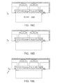
- FIGS. 14B-14C show simulation results of the stress of the film resulting from cleaving utilizing such a constraint plate according to certain embodiments.
- the picture in FIG. 14B shows an S-layer comprising a porous high density polyethylene (HDPE) plastic material of thickness 6.3 mm and having a Young's modulus of 150 MPa, with an applied pressure in the chamber of 1 MPa (about 150 psi).
- the movement of the cleaved film is shown exaggerated in the figure.
- FIG. 14B The simulation shown in FIG. 14B may be compared with that of FIG. 14C .
- FIG. 14C shows an S-layer comprising VITONTM material of thickness 800 um and having a Young's modulus of 20 MPa, again with an applied pressure in the chamber of 1 MPa (about 150 psi).
- the near identical G I and G II energies of these two simulation results are expected, since they have similar Young's Modulus to S-layer thickness ratios.
- An advantage offered by the configuration of FIG. 14A is its simplicity and the relative ease of generating the stresses necessary to propagate an initiated fracture in a pure or dominant moment mode.
- the use of the constraint plate confers the benefit that no blade is needed to perform the cleaving.
- the moment generated by a constant moment configuration using a constraint plate can be derived. This moment shows a simple relationship between plate mechanical properties and the pressure applied to the crack area.
- Tp P-plate thickness
- Ts S-layer thickness
- ⁇ n Net pressure differential to film crack
- ⁇ Ln Net pressure induced film vertical displacement
- ⁇ n ⁇ a ⁇ Lpl /( Ts *(1 /Es+Tp /( Ts*Ep ))
- Ln ⁇ n*Ts *(1 /Es+Tp /( Ts*Ep ))
- c [ 16 *h 3 * ⁇ Ln*E /(3 * ⁇ n )] 1/4
- a mechanically applied vertical displacement or pre-load may be beneficially applied to aid in “locking” the uncleaved substrate to S-layer interface through pressure induced friction. Since the applied pressure must not leak into the substrate to constraint plate interface, a pre-load may also help seal the interface.
- the cleave parameters are:
- the practical use of this method for further propagation from a small initiation area is apparent.
- the “S” crack length value c is about 1.4 mm and consistent with a laser initiated edge area that typically has a length exceeding 4-10 mm.
- the K II 0 condition will occur for a force of about 2e4 N/m.
- the total force required is 3.1 kN or about 700 lbs force, readily achievable with pneumatics, motorized actuators and the like.
- the total linear deformation would be about 454 ppm ⁇ 156 mm or 71 um.
- S-layer displacement can be gradually increased from the cleave location and thus a gradually increasing pressure (and perhaps a P-plate force as well) would be required to achieve threshold cleaving.
- S-layer moment a gradually increasing pressure
- P-plate P force a gradually increasing force
- controlled cleaving according the present invention may be accomplished under conditions where the ratio of K II /K I forces (also referred to herein as mixity), is intentionally balanced utilizing a releasable constraint plate structure.
- FIG. 15 shows a simplified cross-sectional view of one embodiment of such a releasable constraint plate in accordance with the present invention.
- FIG. 15 shows a releasable constraint plate 1500 that is positioned within a telescoping high pressure chamber 1502 defined within walls 1504 .
- the releasable constraint plate 1500 may comprise a plate that can couple side forces (the “P-plate” 1506 ) and a thin, softer compliant layer (the “S-layer” 1508 ) situated between the P-plate and the workpiece or substrate 1510 .
- a second side of the complaint S-layer material is in contact with the upper surface 1510 a of workpiece or substrate 1510 .
- Workpiece or substrate 1510 comprises a cleave initiation portion 1512 and a cleave region 1514 that is located at a depth d from the upper surface. This cleave region may be formed by the energetic implantation of ions, as has been previously described.
- the workpiece is supported within the chamber by a susceptor 1550 .
- This support should be sufficiently rigid to allow for the efficient coupling of vertical displacements and for S-layer pressure coupling.
- a pressure-tight seal is used across interfaces under the workpiece. For example a vacuum seal under the workpiece 1510 using an o-ring or lip seal (discussed in detail below in connection with FIGS. 18 , and 18 A- 18 I) in the peripheral region A 1 would serve as a temporary gas-tight seal.
- a moveable element 1530 is fixed to a wall of the chamber proximate to the location of the cleave initiation portion in the substrate.
- the moveable element comprises a high force motorized actuator that develops a predictable and reproducible amount of physical deformation.
- the moveable element is in physical communication with the side of the compressible P-plate through a rigid armature 1536 .
- this armature is shown as having a rectangular profile, but in other embodiments it may exhibit other shapes or profiles.
- a frictionless 2-dimensional kinematic mounting configuration may be used.
- the P-plate top surface could be connected to a rigid top surface 1560 (which may be a wall or a top plate) via ball bearings 1562 that are contained within pods 1564 .
- the moveable member Upon application of a signal to actuate the moveable member, the moveable member exerts a linear force P in the direction shown by the arrow. This expansion force is in turn translated through the rigid armature that is in contact with a point on the side of the P-plate having a thickness Y.
- the P-plate In response to the linear force received at its side, the P-plate, mostly constrained in the vertical direction experiences compression along the horizontal direction. This is turn develops a force P loading, shown here as +P 1 . Owing to the pressure bonding between the releasable constraint plate and the substrate, this force loading is in turn communicated to the thickness of material of the underlying substrate. This force serves to add to the S-layer pressure induced moment loading +M 1 to permit cleaving to occur along the cleave plane in a controlled manner, allowing the thickness of material to be detached from the substrate.
- this other member may comprise a transfer substrate or chuck used for temporary handling of the thin detached film. In some embodiments, this other member may comprise a portion of the end product in which the detached film is to be incorporated.
- a number of parameters affect the character of the moment and force loading imposed upon the substrate by the releasable constraint plate.
- examples of such parameters include but are not limited to the thicknesses and Young's modulus of the S-layer and P-plate.
- the source of the linear force is a moveable member comprising a motorized actuator.
- suitable actuators are servo actuators such as the EC3 and EC5 available from Kollmorgen of Radford, Va. Force and displacement feedback sensors coupled to the linear actuator as shown in FIG. 15 could help control and measure cleaving.
- embodiments are not limited to embodiments utilizing linear force applied by motorized actuators, and other sources of linear force could be employed.
- One such alternative embodiment could utilize actuation of a hydraulic cylinder to impose the desired linear force upon the releasable plate.
- the linear force could be applied by another type of actuation, for example a piezoelectric material.
- FIG. 15 shows a releasable plate having an S-layer interface
- a lip seal oriented to contact a periphery of the substrate could be used to help seal the workpiece to S-layer interface.
- Embodiments of such a lip seal are shown and described in connection with FIG. 18 .
- a releasable plate according to some embodiments could include porous materials including across the entire surface of the plate in contact with the substrate.
- an initiated region 1602 is formed using an external energy source such as a laser within a higher dose region 1605 along an edge of the substrate 1604 .
- an external energy source such as a laser within a higher dose region 1605 along an edge of the substrate 1604 .
- the initiation region connects to a peripheral portion of the workpiece.
- Laser induced initiation regions typically measure 4-10 mm in diameter in roughly a semicircular shape within the workpiece.
- the workpiece or substrate 1604 is placed into contact with the releasable constraint plate 1606 .
- a thickness of material 1608 to be detached from substrate 1604 is defined between surface 1604 a and cleave initiation portion 1602 and cleave region 1610 . Selected applications of S-layer pressures and P-plate side forces will complete the remaining steps as explained below.
- the second and third cleave steps have the substrate and the releasable plate positioned within a pressure volume 1620 that is in selective communication with a source of high pressure 1622 .
- the bottom of the substrate may be positioned on a chuck or other type of support 1624 .
- a pressure difference p is applied within the pressure vessel, that in turn acts to create a moment to extend the initiation region from a small edge defined area to a tab spanning a portion of the higher dose region 1605 .
- the pre-load vertical displacement, dose profile and pressure are controlled to develop a first propagation that forms a “tab” 1650 of sufficient width to allow the lower dose third cleave step to occur.
- the side force P is now applied and couple to the now relatively well formed crack front to propagate the cleave front in a controlled manner through the lower dose region.
- the S-layer in turn transfers this mechanical force to the surface of the substrate.
- This force can be used to perform controlled cleaving of the thickness of detachable material from the substrate.
- FIG. 17 thus shows one possible alternative embodiment wherein the releasable plate 1700 is selectively secured in place at certain of its edges, by anchors 1702 .
- This configuration serves to restrict deformation of the plate in the direction of one axis (here the X-axis), while permitting deformation in the direction of another axis (the Y-axis).
- Such control over the manner of deformation of the releasable plate can in turn allow control to be exercised over the direction of mechanical forces imposed during controlled cleaving.
- a thickness of material may be detached from a substrate by controlled cleaving along a cleave plane.
- controlled cleaving with a desired mixity of K II and K I fracture modes may be achieved utilizing a releasable constraint plate that is adhered to the substrate surface.
- Certain embodiments may employ controlled cleaving utilizing a plate which maintains dominance of K I forces during cleaving.
- Alternative embodiments may employed controlled cleaving utilizing a plate with maintains dominance of K II forces during cleaving. Thicknesses of material detached by controlled cleaving according to embodiments of the present invention may be particularly suited for incorporation into solar cells.
- the particles of hydrogen can be replaced using co-implantation of helium and hydrogen ions to allow for formation of the cleave plane with a modified dose and/or cleaving properties according to alternative embodiments.
- the backing substrate can be applied to each of the substrates, including handle and donor.
- coatings may also be provided on surfaces or other regions of the transparent material. Therefore, the above description and illustrations should not be taken as limiting the scope of the present invention which is defined by the appended claims.
- a first fracture mode comprises an opening or tensile mode (K I ), where cleaving forces act substantially perpendicular to a direction in which the cleave front is propagating.
- a second fracture mode comprises a shearing or sliding mode (K II ), where cleaving forces lie substantially parallel to the direction in which the cleave front is propagating.
- a third fracture mode comprises a tearing or out-of-plane mode (K III ), where cleaving forces are substantially out of a plane along which the cleaving is occurring.
- FIG. 11 shows a simplified view of an embodiment of a workpiece 1102 having a cleave plane 1106 formed therein.
- the cleave plane affects the cleaving action through stress and layer weakening effects.
- the cleave plane may be formed by energetic implantation of ions (such as hydrogen) into the workpiece. Such implantation is discussed in U.S. Patent Publication Nos. 2008/0206962, and 2008/0128641, both of which are incorporated by reference in their entireties herein for all purposes.
- the cleave plane can be used both as an initiating layer at higher doses, and as a guiding or propagating layer when the dose is lower. Cleave guiding at lower doses is mostly dominated by the implanted hydrogen compressive stress profile.
- FIG. 13 shows the mechanical configuration of cleave propagation following an initiation process.
- FIG. 13 shows a layer of thickness h partially released from the rest of the silicon ingot substrate having thickness H. Due to the much larger dimensions of the substrate relative to the cleaved material (h ⁇ H), the tile moment and forces M 2 , P 2 , and M 3 , P 3 are understood to be very small. The source of stress intensity seen at the crack tip is thus dominated by M 1 and P 1 , the moment and force coupled to the partially released film.
- the implanted hydrogen compressive stress profile helps keep the cleave front propagating along the cleave plane.
- a cleave guiding effect is the shear force generated by the in-plane compressive layer that is generated when the cleave front moves away from the center of the compressive stress profile.
- Deviation of the cleave front depth away from this center point of compressive stress will tend to generate an in-plane (K II ) shear force having a polarity that tries to maintain the cleave front propagating parallel to and within the cleave plane over some range of shear stress intensity values (non-zero K II ).
- K II in-plane
- a positive (K II ) shear force will guide the cleave front lower towards the center.
- a negative K II shear force will guide the cleave front higher towards the center. This phenomenon occurs because any non-zero K II generated during cleaving will tend to guide the fracture plane away from the cleave plane so as to minimize K II .
- the effect can be modeled by a capture range of K II stress intensities within which the cleave propagation direction continues to lie parallel and close to the K II ⁇ 0 fracture propagation plane.
- Certain embodiments of the present invention relate to controlled cleaving along an implanted subsurface cleave plane within a semiconductor workpiece. Particular embodiments allow independent application of a linear cleaving shear force (+P 1 ) coordinated with an independent application of a cleaving moment (+M 1 ).
- the cleaving moment (+M 1 ) drives the cleaving through a combination of opening or tensile stress intensity (K I ) and shear stress intensity (K II ).
- K I opening or tensile stress intensity
- K II shear stress intensity
- the linear cleaving shear force (+P 1 ) counteracts a tendency of the cleave front to move out of the implanted cleave plane through moment alone.
- FIG. 18 shows a simplified cross-sectional view of a cleaving apparatus in accordance with one embodiment of the present invention. Specifically, a backside 1802 A of workpiece 1802 is in contact with an adapter piece 1805 that includes channels allowing suction from a vacuum chuck 1803 to secure the workpiece against a seal 1855 .
- the adapter piece 1805 is also responsible for ensuring the proper placement of the workpiece relative to other elements of the apparatus, for example the S-layer as described further below.
- the vacuum chuck is moveably connected to elevator 1804 whose movement in the vertical direction can allow loading and unloading of the workpiece therefrom.
- the elevator is in contact with actuators 1840 - 1842 that can also impart a limited tilt to the workpiece 1802 .
- Load cells 1880 can determine the relative forces on the actuators 1840 - 1842 .
- the seal may be in the form of an o-ring or other pliant member in contact with the workpiece backside, with the o-ring sealed by the suction force of the vacuum.
- the seal 1855 may comprise a lip-seal in contact with the sides of the workpiece, as is further described in detail below.
- the o-ring or other pliant member positioned close to the perimeter of the workpiece as is feasible. This maximizes the area of the workpiece exposed to the vacuum to ensure that no separation occurs between the workpiece 1802 and chuck 1803 as chamber pressures vary from ambient (e.g. during loading/unloading) to high (e.g. during application of the cleaving pressure). Assuming the top of the workpiece is evacuated to atmosphere, this lifting effect can occur when the bottom area exposed to p subjects the workpiece to an upward force that exceeds the downward force developed by the area under vacuum.
- a first end 1806 of workpiece 1802 includes a subsurface high dose implanted cleave initiation region 1808 .
- a subsurface lower dose implanted cleave propagation region 1810 extends outside of the cleave initiation region.
- Workpiece 1802 further includes a cleaved portion 1809 within the cleave initiation region 1808 .
- FIG. 18 is not drawn to scale for purposes of illustration, and thus the dimensions of the cleaved portion are grossly exaggerated in this figure.
- the cleaved portion 1808 may be formed by the localized application of concentrated thermal energy to the cleave initiation region.
- the cleaved portion may be formed by a laser, for example as is described in the pending U.S. patent application Ser. No. 13/195,259 that is incorporated by reference in its entirety herein for all purposes.
- Elevator 1804 is moveable in the vertical direction (Z-axis) to position the workpiece within the surrounding sealing member 1811 .
- the frontside 1802 B of workpiece 1802 is in contact with porous compliant S-layer 1812 that is supported upon lower surface 1814 a of P-plate 1814 .
- This S-layer is porous and hence able to evacuate the workpiece to a secondary pressure, usually atmospheric pressure.
- the S-layer is also compliant to accommodate forces during the cleaving process.
- An example of the material forming the S-layer is DELRIN Acetal Resin (Polyoxymethylene) thermoplastic available from DuPont, Wilmington, Del., USA.
- Plate 1814 includes a projecting region 1814 a corresponding to the first end of the workpiece. The opposite end of the plate is fixed in the horizontal direction (X-axis).
- Actuator 1815 may extend in the horizontal direction to physically contact the projecting portion. As is further discussed in detail below, such horizontal actuation of the actuator against the projecting portion results in the production of a linear cleaving shear force (+P 1 ) being exerted upon the cleaved portion. The workpiece is secured in place from the opposite direction by member 1860 .
- FIGS. 18A-18B show the operation of the lip seal.
- FIG. 18A shows the contacting of workpiece 1802 comprising cleave propagation region 1810 , with the porous S-layer 1812 prior to sealing.
- a lip seal structure 1870 comprising a sealing member 1874 that includes a flexible portion 1876 .
- the sealing member 1874 can comprise different flexible materials, and in certain embodiments can comprise for example HT-6210 liquid silicone rubber sheeting from Rogers Corporation, Carol Stream, Ill., USA.
- the sealing member 1874 may be secured to the P-plate by the pressing of an o-ring 1872 into a recess therein, resulting in the flexible portion 1876 projecting upward away from the surface of the K-plate. As shown in FIG. 18A , this configuration is desirable in that prior to the sealing step, it allows vertical movement of the workpiece past the flexible member to contact the porous member. In certain embodiments, the pressing of the o-ring into the recess and the corresponding raising of the lip seal can occur by virtue of upward movement of the elevator forcing the o-ring into the recess.
- An alternative embodiment in the form of a frame surrounding the workpiece and incorporating the lip seal material could also be used.
- FIG. 18B shows the sealing step.
- the flexible portion 1876 of the sealing member 1874 is pulled against the side of the workpiece to create the seal.
- this pressure differential would be attributable solely to a lower pressure V such as a vacuum.
- V such as a vacuum.
- flexible elastomers are of a self-energizing type, the application of a positive pressure within the chamber to accomplish cleaving enhances the sealing effect of the lip seal.
- the sealing could be further assisted by actively disposing the flexible portion against the side of the workpiece, for example utilizing a positive pressure or other approach.
- the lip seal is present around nearly the entire perimeter of the P-plate. However, as shown in FIG. 18 , in certain embodiments the lip seal does not extend to a local area proximate to the cleave initiation region. This is to allow the positive pressure within the chamber to gain access to the cleave initiation region and thereby contribute to the controlled cleaving. To prevent unwanted leakage in this limited area, portions of the surface of the S-layer corresponding to regions lacking the lip seal, may bear a non-porous coating 1877 .
- a seal may extend around the entire perimeter of the P-plate. Injection of the initiation pressure can be made within the gastight region defined by a lip seal conforming against a side of the workpiece, through a port or channel machined within the P-plate. According to some embodiments, gas pressure injection in a dynamic manner is possible. Such dynamic pulsed pressure involves the application of a pressure that changes over time, for example in certain embodiments a pulse of increased pressure from a second gas source that is applied locally to the initiation region through a channel in the P-plate. Dynamic application of pressure during cleaving according to certain embodiments may offer the benefit of allowing better threshold cleave control.
- a pressurized gas from a source 1821 is introduced through a port in the high pressure vessel.
- pressurization of the gastight region in this manner or through a separate port as described above results in a moment cleaving force (+M 1 ) being exerted upon the cleaved portion.
- P-Plate 1814 is secured from movement in the vertical direction, by contact with stiff support 1830 .
- the stiff support is in turn secured an overall support structure that has enough overall stiffness to allow only limited flexure under loading.
- the elevator is fixed to three linear actuators 1840 - 1842 . These actuators are independently actuable. Their points of contact with the elevator allow the three-dimensional position of the elevator to be altered. Where the elevator is fixed in position by virtue of the loading of the workpiece, selective actuation of the linear actuators allows the application of force in the vertical direction, per the pre-loading and loading discussions below.
- FIG. 18 shows the three linear actuators as being in contact with the elevator, this is not required. Alternative embodiments could employ linear actuators in contact with the stiff support so as to apply forces to the workpiece.
- the various components of the system are in electronic communication with a central processor 1850 that is in communication with computer-readable storage unit 1852 .
- the processor is configured to coordinate operation of the system elements based upon instructions from code stored within the unit 1852 .
- the various operational modes of the processor and stored codes instructing same, are discussed further below.
- Cleaving may rely upon a fixed grip between the compliant plate and the workpiece, as reflected for example by an unchanging vertical distance between the bottom of the workpiece and the top of the P-plate.
- the chamber may include a vertical distance gauge to measure this distance.
- An example of such a vertical distance gauge which may be suitable for use in accordance with the present invention, is available from HEIDENHAIN CORPORATION, of Schaumburg, Ill. Such gauges can be used to control the actuators 1840 - 1842 through a servo loop to maintain a fixed grip configuration through the large force changes that occur during cleaving.
- FIGS. 18C-H show the disposition of forces in three-dimensions on the P-plate/S-layer and workpiece, with other elements of the apparatus omitted for clarity.
- a computer pre-processing (calibration) phase is shown in FIG. 18C .
- a workpiece blank 1890 is disposed in contact with the plate, and the apparatus is calibrated. Examples of such calibration include the initial position of the elements in three-dimensional space, the setting of the vertical distance gauge, and the force readings of each of the actuators. In this neutral force state, the P-plate and the S-layer are experience little or no compression.
- a workpiece insertion phase is shown in FIG. 18D .
- the elevator is raised such that the workpiece including the cleave plane and the cleaved portion, comes into contact with the S-layer in the plate.
- the elevator is raised until the readings of the load cells reflect the exertion of predetermined forces in the Z-direction.
- the vertical position of the elevator is then locked in place.
- the voltages applied to the actuators are finely adjusted to re-establish the original calibrated neutral force state.
- the setting of the vertical distance gauge is set to zero.
- the lip seals are engaged to create the gastight seal around the cleaved portion.
- net forces in the vertical direction may be applied to the workpiece by the linear actuator structures acting through the elevator and the chuck.
- the preloading forces should be sufficient to maintain sealing between the workpiece and the S-layer and discourage cleaving upon first application of the pressure p.
- this pre-loading force may be uniform over the workpiece area.
- a non-uniform pre-loading force may be applied in this phase. Such a situation is akin to causing the actuators to tilt the elevator in space, except that any movement of the stiff support in the Z-direction is constrained, thereby creating a force.
- Such a non-uniform pre-loading force may represent a force distribution within the orthogonal surface axes of the workpiece.
- a greater pre-loading force may be applied to the portion of the wafer opposite the cleave initiation region.
- a non-uniform pre-loading force may serve to arrest cleave propagation, desirably allowing for incremental cleaving across the wafer in a controlled manner.
- FIG. 18F shows a first loading phase.
- a (moment) loading force is applied to the workpiece.
- a compressed gas is flowed from a source into the chamber.
- This compressed gas creates a pressure in the gap extant between the cleaved portion and the remaining underlying material of the workpiece.
- the upward pressure of the compressed gas within the gap exerts a moment cleaving force (+M 1 ) on the cleaved portion.
- Flexion in the compliant gripping layer accommodates movement of the cleaved portion in response to the moment, thereby allowing propagation of the cleave front in the lateral direction.
- This positive moment (+M 1 ) can be used to develop a tab of large enough width within the higher dose region 1808 and its immediate surroundings.
- a second loading phase is shown in FIG. 18G .
- a second linear loading force is applied to the workpiece.
- the actuator exerts a horizontal force against the projecting portion of the plate, sufficient to compress the plate along its lateral dimension to some extent. This compression of the plate produces some corresponding amount of horizontal movement relative to the stiff support along the X-axis. This horizontal movement is accommodated by the presence of the intervening ball bearings.
- the slight horizontal movement of the plate, while the workpiece remains fixed in position exerts a linear cleaving shear force (+P 1 ) on the cleaved portion of the workpiece. This force is communicated from the plate to the workpiece by the grip of the S-layer.
- the combination of linear cleaving shear force (+P 1 ) and moment cleaving force (+M 1 ) acting upon the cleaved portion serves to propagate cleaving in a highly uniform manner.
- the +P 1 and +M 1 cleaving forces are precisely and carefully controlled to achieve a mixity of fracture modes (K II /K I ) of near-zero (K II ⁇ 0). This allows the cleave front to extend into the cleave propagation region with little change in depth and without fracture of the thin and delicate cleaved portion.
- FIG. 18I shows a simplified plan view of the workpiece and the plate from the perspective of the chuck.
- the width W of the ring 1899 can determine the magnitude of the linear shear cleaving stress by reducing it linearly as the cleave progresses.
- the increased width of the ring in the direction away from the piston serves to reduce the effective +P 1 experienced by the top surface of the workpiece, thereby self-arresting unlimited cleaving from propagating indefinitely in an uncontrolled manner.
- the actuators can subsequently be monitored in order to detect an overall percentage of cleaving that has taken place across the workpiece.
- FIG. 19 plots the force in the Z-direction against the workpiece (as measured by the load cell readings), versus the time of application of the compressed gas to the chamber.
- the load cells indicate a constant force over (A) until initiation starts (sudden jump at B). As the cleave progresses, there would be a linear increase in the force measured by the load cells.
- the constant force in part A says that the gas pressure is not changing and the cleave has not started.
- FIG. 19 shows an interval A in which the cumulative pressure of the compressed gas is not sufficient to generate a large enough cleaving moment to begin the cleaving action. This region A is indicated in the graph by no change in the force along the vertical direction.
- FIG. 19 shows that a point B, pressure of the compressed gas creates a moment sufficient to begin the controlled cleaving action. This is indicated in the graph by an abrupt increase in the signal from the load cells.
- FIG. 19 further shows that over the subsequent interval C, the pressure of the compressed gas and the linear force imparted to the P-plate propagates the controlled cleaving. This is indicated in the graph by a positive slope indicating progressively larger area of the brick is being cleaved and therefore exposed to the higher pressure.
- FIG. 20 shows a simplified view of such a processor 2000 , including the various inputs and outputs.
- FIG. 20 shows processor 2000 receiving input signals 506 indicating the readings from the actuator encoders.
- Processor 2000 is further configured to receive inputs 2008 a - b indicating the vertical height elevator, and a digital signal indicating the locking status of the elevator, respectively.
- Processor 2000 is still further configured to receive a digital REF/HOME signal 2010 indicative of the start condition for operation.
- Processor 2000 also receives input 2012 indicating the pressure of the compressed gas, and input 2014 indicating the force being applied by the actuator.
- Processor 2000 is also configured to correspondingly produce a number of different output signals.
- One output is a feedback signal 2022 to the piston actuator, to ensure application of the appropriate linear cleaving shear force (+P 1 ) for achieving the desired mixity (K II ⁇ 0).
- Signal 2024 Setting the forces exerted by the actuators.
- Signal 2022 is the P-force feedback.
- These parameters may be changed between successive cleaving processes of different workpieces. Moreover, these parameters may also be varied within a cleaving process, for example to self-arrest unlimited cleaving from propagating in an uncontrolled manner. This is described above in connection with FIG. 18H .
- Other parameter variations that may have a similar effect include decreasing the thickness of the compliant layer away from the initiation region, or increasing a pre-loading force away from the initiation region.
- FIG. 18 While the embodiment discussed above in connection with FIG. 18 features an apparatus having an S-layer in direct contact with the workpiece, this is not required. Alternative embodiments could utilize a separate layer for gripping the workpiece. Such a gripping material would be calculated to exhibit both the desired amount of lateral compression, and the compliant, gripping characteristic in the vertical direction. Moreover, where vacuum force is used for sealing, the separate gripping layer should exhibit the desired porosity.
- Certain embodiments could employ separate materials for the gripping and compliant characteristics. Such an embodiment could feature a compliant layer having the desired Young's modulus, and could also feature an intervening thin membrane composed of a different material having a sufficiently high coefficient of friction to ensure maintenance of the proper grip between the compliant layer and the workpiece.
- FIG. 18 shows an embodiment of an apparatus that features a porous constraint plate sealed to the workpiece utilizing a vacuum and a lip seal, this is not required.
- Alternative embodiments could employ the application of other types of sealing forces and sealing structures.
- an alternative embodiment could employ an S-layer having channels formed therein to allow the maintenance of a top pressure to develop the desired cleaving moment within the workpiece.
Landscapes
- Engineering & Computer Science (AREA)
- Life Sciences & Earth Sciences (AREA)
- Forests & Forestry (AREA)
- Mechanical Engineering (AREA)
- Photovoltaic Devices (AREA)
- Manufacturing & Machinery (AREA)
- Chemical & Material Sciences (AREA)
- Crystallography & Structural Chemistry (AREA)
- Sustainable Development (AREA)
- Sustainable Energy (AREA)
Abstract
Description
γ′=αH 2*γ, (1)
where:
αH is a factor between 0 and 1 that serves to quantify the reduction in cleave energy due to hydrogen embrittlement.
αH=1/(1+K H*φ), (2)
where:
KH is a constant to be determined experimentally, and φ is the hydrogen dose.
γ′=[1/(1+K H*φ)]2*γ (3)
Since the cleaving energy is a fundamental parameter in linear elastic fracture mechanics, the correlation between implant dose and energy allow accurate prediction and modeling of cleaving action.
G′=2*γ′=2*αH 2*γ (4)
where E′=the plane strain equation defined as E′=E/(1−ν2), and, for all purposes of this document, G is G′ and generally related to the cleave plane by equation (4):
G′=2*γ′=2*αH 2*γ (4)
Where Pn and Mn are the forces and moments respectively, acting on each of the members.
the parameters are derived from the forces, moments and geometry as described in detail by Hutchinson and Suo, “Mixed Mode Cracking in Layered Materials”, Advances in Applied Mechanics, Vol. 29 (1992), which is incorporated by reference in its entirety herein for all purposes.
σn=σa−ΔLpl/(Ts*(1/Es+Tp/(Ts*Ep))
ΔLn=σn*Ts*(1/Es+Tp/(Ts*Ep))
G=energy release in crack=σ*ΔL
M=[σn*h 3 *ΔLn*E/6]1/2
c=[16*h 3 *ΔLn*E/(3*σn)]1/4
- M=0.147 N-m/m
- G=5.19 J/m2 with mixity of −37 degrees
- c=1.36 mm
- ΔLn=14.5 um
| Film | Moment M | Force P | Film Strain | |
| Thickness (um) | (N-m/m) | (N/m) | (ppm) | |
| 20 | 0.021 | 2.7 × 10³ | 722 | |
| 50 | 0.079 | 4.3 × 10³ | 454 | |
| 150 | 0.412 | 7.3 × 10³ | 260 | |
Force=Strain*Ep*Tp, where Force is in Newtons per unit depth (N/m)
| PARAMETER | CHANGE | RESULT | |
| Compressed gas pressure | Increase | Increase (+M1) | |
| Decrease | Decrease (+M1) | ||
| Actuator P-plate force | Increase | Increase (+P1) | |
| Decrease | Decrease (+P1) | ||
| Young's modulus of P-plate | Increase | Decrease (+P1) | |
| Decrease | Increase (+P1) | ||
| Young's modulus of S-layer | Increase | Decrease (+M1) | |
| Decrease | Increase (+M1) | ||
| Width of plate | Increase | Decrease (+P1) | |
| Decrease | Increase (+P1) | ||
| Thickness of S-layer | Increase | Increase (+M1) | |
| Decrease | Decrease (+M1) | ||
| Dose of cleave plane | Increase | Decrease (+M1), | |
| Increase (−P1) | |||
| Decrease | Increase (+M1), | ||
| Decrease (−P1) | |||
| Pre-load force | Increase | Decrease (+M1) | |
| Decrease | Increase (+M1) | ||
| CHARACTERISTIC | VALUE |
| Workpiece | |
| Workpiece material | Mono-Si (111) |
| Workpiece thickness (H) | 5 to 100 mm |
| Workpiece Young's Modulus | 187 GPa |
| Surface Energy | 2.4 J/m2 |
| Cleave Plane | |
| Cleaved layer thickness (h) | 20 to 150 μm |
| Cleaved portion length (l) | 60 to 156 mm |
| Implanted ion | |
| Implant Energy | |
| 1 to 4 (MeV) | |
| Initiation region dose | 6-9e16 (atoms/cm2) |
| |
1 to 6e16 (atoms/cm2) |
| Cleave Moment | |
| Compliant layer material | Porous HDPE |
| Compliant layer Young's Modulus | 150 MPa |
| Compliant layer thickness | 6.3 |
| Pre-load pressure | |
| 0 to compressed gas pressure | |
| value (0 in example) | |
| Compressed Gas Pressure | 0-150 PSI (40 PSI in example) |
| +M1 | 0.08 N-m/m (40 PSI and 0 PSI |
| Pre-load) | |
| Linear P-Plate | |
| Plate material | Delrin Acetal Resin Plastic |
| Plate Young's Modulus | 2.2 GPa |
| Plate width | 300 mm |
| Actuator (Piston) Force | 10,000 N/m on P-plate |
| (3000 N in example) | |
| +P1 | 4,280 N/m in example |
| KI | 0.712 MPa-m1/2 |
| KII | −0.007 MPa-m1/2 |
| Mixity (KII/KI) | −0.01 |
Claims (20)
Priority Applications (3)
| Application Number | Priority Date | Filing Date | Title |
|---|---|---|---|
| US13/225,172 US8993410B2 (en) | 2006-09-08 | 2011-09-02 | Substrate cleaving under controlled stress conditions |
| US14/618,940 US9356181B2 (en) | 2006-09-08 | 2015-02-10 | Substrate cleaving under controlled stress conditions |
| US15/167,291 US9640711B2 (en) | 2006-09-08 | 2016-05-27 | Substrate cleaving under controlled stress conditions |
Applications Claiming Priority (8)
| Application Number | Priority Date | Filing Date | Title |
|---|---|---|---|
| US82509506P | 2006-09-08 | 2006-09-08 | |
| US11/852,088 US7811900B2 (en) | 2006-09-08 | 2007-09-07 | Method and structure for fabricating solar cells using a thick layer transfer process |
| US5130708P | 2008-05-07 | 2008-05-07 | |
| US9268308P | 2008-08-28 | 2008-08-28 | |
| US12/435,230 US9362439B2 (en) | 2008-05-07 | 2009-05-04 | Layer transfer of films utilizing controlled shear region |
| US12/460,898 US8293619B2 (en) | 2008-08-28 | 2009-07-24 | Layer transfer of films utilizing controlled propagation |
| US12/730,113 US8110480B2 (en) | 2006-09-08 | 2010-03-23 | Method and structure for fabricating solar cells using a thick layer transfer process |
| US13/225,172 US8993410B2 (en) | 2006-09-08 | 2011-09-02 | Substrate cleaving under controlled stress conditions |
Related Parent Applications (3)
| Application Number | Title | Priority Date | Filing Date |
|---|---|---|---|
| US12/435,230 Continuation-In-Part US9362439B2 (en) | 2006-09-08 | 2009-05-04 | Layer transfer of films utilizing controlled shear region |
| US12/460,898 Continuation-In-Part US8293619B2 (en) | 2006-09-08 | 2009-07-24 | Layer transfer of films utilizing controlled propagation |
| US12/730,113 Continuation-In-Part US8110480B2 (en) | 2006-09-08 | 2010-03-23 | Method and structure for fabricating solar cells using a thick layer transfer process |
Related Child Applications (1)
| Application Number | Title | Priority Date | Filing Date |
|---|---|---|---|
| US14/618,940 Division US9356181B2 (en) | 2006-09-08 | 2015-02-10 | Substrate cleaving under controlled stress conditions |
Publications (2)
| Publication Number | Publication Date |
|---|---|
| US20120234887A1 US20120234887A1 (en) | 2012-09-20 |
| US8993410B2 true US8993410B2 (en) | 2015-03-31 |
Family
ID=46827671
Family Applications (3)
| Application Number | Title | Priority Date | Filing Date |
|---|---|---|---|
| US13/225,172 Expired - Fee Related US8993410B2 (en) | 2006-09-08 | 2011-09-02 | Substrate cleaving under controlled stress conditions |
| US14/618,940 Expired - Fee Related US9356181B2 (en) | 2006-09-08 | 2015-02-10 | Substrate cleaving under controlled stress conditions |
| US15/167,291 Active - Reinstated US9640711B2 (en) | 2006-09-08 | 2016-05-27 | Substrate cleaving under controlled stress conditions |
Family Applications After (2)
| Application Number | Title | Priority Date | Filing Date |
|---|---|---|---|
| US14/618,940 Expired - Fee Related US9356181B2 (en) | 2006-09-08 | 2015-02-10 | Substrate cleaving under controlled stress conditions |
| US15/167,291 Active - Reinstated US9640711B2 (en) | 2006-09-08 | 2016-05-27 | Substrate cleaving under controlled stress conditions |
Country Status (1)
| Country | Link |
|---|---|
| US (3) | US8993410B2 (en) |
Cited By (7)
| Publication number | Priority date | Publication date | Assignee | Title |
|---|---|---|---|---|
| US20140339681A1 (en) * | 2011-09-20 | 2014-11-20 | Soitec | Method for fabricating a composite structure to be separated by exfoliation |
| US9336989B2 (en) | 2012-02-13 | 2016-05-10 | Silicon Genesis Corporation | Method of cleaving a thin sapphire layer from a bulk material by implanting a plurality of particles and performing a controlled cleaving process |
| US9640711B2 (en) * | 2006-09-08 | 2017-05-02 | Silicon Genesis Corporation | Substrate cleaving under controlled stress conditions |
| US10910272B1 (en) * | 2019-10-22 | 2021-02-02 | Sandisk Technologies Llc | Reusable support substrate for formation and transfer of semiconductor devices and methods of using the same |
| CN113228232A (en) * | 2018-12-29 | 2021-08-06 | 克利公司 | Carrier-assisted method for separating crystalline material along laser damage regions |
| TWI821529B (en) * | 2019-03-15 | 2023-11-11 | 法商索泰克公司 | Holding device for a fracturable assembly and separation equipment for separating the fracturable assembly |
| US20240006218A1 (en) * | 2022-06-30 | 2024-01-04 | Infineon Technologies Ag | Method of manufacturing a semiconductor device |
Families Citing this family (37)
| Publication number | Priority date | Publication date | Assignee | Title |
|---|---|---|---|---|
| JP5417399B2 (en) * | 2011-09-15 | 2014-02-12 | 信越化学工業株式会社 | Manufacturing method of composite wafer |
| US20130144421A1 (en) * | 2011-12-01 | 2013-06-06 | Memc Electronic Materials, Spa | Systems For Controlling Temperature Of Bearings In A Wire Saw |
| DE112012006750B4 (en) * | 2012-07-30 | 2026-01-08 | Erich Thallner | Substrate composite, method and device for bonding substrates |
| FR3000109B1 (en) * | 2012-12-21 | 2015-01-16 | Commissariat Energie Atomique | PROCESS FOR PRODUCING A THICK CRYSTALLINE LAYER |
| JP2016511934A (en) * | 2013-01-16 | 2016-04-21 | キューマット インコーポレイテッドQmat, Inc. | Technology for forming optoelectronic devices |
| US9875935B2 (en) * | 2013-03-08 | 2018-01-23 | Infineon Technologies Austria Ag | Semiconductor device and method for producing the same |
| US10421208B2 (en) * | 2013-03-12 | 2019-09-24 | Sunpower Corporation | Method and device for cleaving wafers |
| FR3003692B1 (en) * | 2013-03-25 | 2015-04-10 | Commissariat Energie Atomique | METHOD FOR MANUFACTURING A MULTIJUNCTION STRUCTURE FOR A PHOTOVOLTAIC CELL |
| DE102013103495A1 (en) * | 2013-04-08 | 2014-10-09 | Institut Für Solarenergieforschung Gmbh | Method for producing a silicon substrate for solar cell production |
| DE102013014623A1 (en) * | 2013-09-02 | 2015-03-05 | Siltectra Gmbh | Device and method for producing a wafer with a selective positioning in the carrier system |
| DE102013014615A1 (en) * | 2013-09-02 | 2015-03-05 | Siltectra Gmbh | Device and method for producing a wafer with a crack course influencing |
| DE102013016669A1 (en) * | 2013-10-08 | 2015-04-09 | Siltectra Gmbh | Combined manufacturing process for separating a plurality of thin solid layers from a thick solid |
| CN105848841B (en) * | 2013-12-27 | 2017-07-28 | 旭硝子株式会社 | Processing method of brittle plate and processing device of brittle plate |
| GB201401115D0 (en) * | 2014-01-23 | 2014-03-12 | Johnson Matthey Plc | Diesel oxidation catalyst and exhaust system |
| US9523158B2 (en) * | 2014-02-07 | 2016-12-20 | Applied Materials, Inc. | Methods and apparatus for forming semiconductor |
| US9899499B2 (en) * | 2014-09-04 | 2018-02-20 | Sunedison Semiconductor Limited (Uen201334164H) | High resistivity silicon-on-insulator wafer manufacturing method for reducing substrate loss |
| KR20180010274A (en) | 2015-06-19 | 2018-01-30 | 큐맷, 인코포레이티드 | Bond and release layer transport process |
| US10828800B2 (en) | 2016-03-08 | 2020-11-10 | Arizona Board Of Regents On Behalf Of Arizona State University | Sound-assisted crack propagation for semiconductor wafering |
| US11130200B2 (en) | 2016-03-22 | 2021-09-28 | Siltectra Gmbh | Combined laser treatment of a solid body to be split |
| US10297445B2 (en) | 2016-06-14 | 2019-05-21 | QROMIS, Inc. | Engineered substrate structure for power and RF applications |
| WO2018011731A1 (en) * | 2016-07-12 | 2018-01-18 | QMAT, Inc. | Method of a donor substrate undergoing reclamation |
| US20180019169A1 (en) * | 2016-07-12 | 2018-01-18 | QMAT, Inc. | Backing substrate stabilizing donor substrate for implant or reclamation |
| US20180033609A1 (en) * | 2016-07-28 | 2018-02-01 | QMAT, Inc. | Removal of non-cleaved/non-transferred material from donor substrate |
| US10978311B2 (en) * | 2016-12-12 | 2021-04-13 | Siltectra Gmbh | Method for thinning solid body layers provided with components |
| EP3586356B1 (en) * | 2017-02-21 | 2023-11-08 | EV Group E. Thallner GmbH | Method for bonding substrates |
| US10991617B2 (en) | 2018-05-15 | 2021-04-27 | Applied Materials, Inc. | Methods and apparatus for cleaving of semiconductor substrates |
| CN109227693B (en) * | 2018-08-31 | 2024-03-22 | 合肥泰沃达智能装备有限公司 | A light guide plate cutting auxiliary mechanism |
| US10562130B1 (en) | 2018-12-29 | 2020-02-18 | Cree, Inc. | Laser-assisted method for parting crystalline material |
| US10576585B1 (en) | 2018-12-29 | 2020-03-03 | Cree, Inc. | Laser-assisted method for parting crystalline material |
| FR3093859B1 (en) * | 2019-03-15 | 2021-02-12 | Soitec Silicon On Insulator | Method of transferring a useful layer onto a support substrate |
| US10611052B1 (en) | 2019-05-17 | 2020-04-07 | Cree, Inc. | Silicon carbide wafers with relaxed positive bow and related methods |
| US11538698B2 (en) | 2019-09-27 | 2022-12-27 | Globalwafers Co., Ltd. | Cleave systems having spring members for cleaving a semiconductor structure and methods for cleaving such structures |
| CN112967982B (en) * | 2020-09-10 | 2022-04-19 | 重庆康佳光电技术研究院有限公司 | Transfer substrate, manufacturing method of transfer substrate, chip transfer method and display panel |
| CN112861278B (en) * | 2021-01-06 | 2022-04-15 | 上海理工大学 | Method for calculating length of initial cleavage crack of semiconductor material |
| WO2022255976A2 (en) * | 2021-05-31 | 2022-12-08 | Orta Doğu Tekni̇k Üni̇versi̇tesi̇ | Method of obtaining membranes and other functional films by aligned deposition of nanorod structured materials on porous surfaces via cross flow |
| US11978820B2 (en) * | 2022-09-20 | 2024-05-07 | Semivation, LLC | Thin single-crystal silicon solar cells mounted to a structural support member and method of fabricating |
| CN115946036B (en) * | 2022-12-15 | 2025-08-05 | 北京晶亦精微科技股份有限公司 | A grinding pressure dressing method, device, computer equipment and medium |
Citations (309)
| Publication number | Priority date | Publication date | Assignee | Title |
|---|---|---|---|---|
| DE834363C (en) | 1951-02-27 | 1952-03-20 | Zentral Werkstatt Goettingen | Method and device for the production of thin mica films |
| US2614055A (en) | 1947-05-12 | 1952-10-14 | Samica Corp | Method of treating mica |
| US3117002A (en) | 1960-02-16 | 1964-01-07 | Ampco Metal Inc | Aluminum bronze alloy having improved wear resistance by the addition of cobalt, chromium, and manganese |
| US3225820A (en) | 1962-11-01 | 1965-12-28 | Gen Precision Inc | Device for controlling temperature by heat conduction |
| US3390033A (en) | 1964-08-13 | 1968-06-25 | Rca Corp | Method of separating frit sealed parts of an electron tube |
| US3392069A (en) | 1963-07-17 | 1968-07-09 | Siemens Ag | Method for producing pure polished surfaces on semiconductor bodies |
| FR1558881A (en) | 1967-05-29 | 1969-02-28 | ||
| US3551213A (en) | 1968-09-04 | 1970-12-29 | Bell Telephone Labor Inc | Geometrically selective ion bombardment by means of the photoelectric effect |
| US3770499A (en) | 1972-02-28 | 1973-11-06 | Motorola Inc | Liquid phase deposition of thin insulating and refractory film on a substrate |
| US3786359A (en) | 1969-03-28 | 1974-01-15 | Alpha Ind Inc | Ion accelerator and ion species selector |
| US3806380A (en) | 1971-03-05 | 1974-04-23 | Hitachi Ltd | Method for hardening treatment of aluminum or aluminum-base alloy |
| US3832219A (en) | 1971-04-07 | 1974-08-27 | Atomic Energy Authority Uk | Methods of treating steel surfaces to modify their structure |
| FR2235474A1 (en) | 1973-06-28 | 1975-01-24 | Ibm | |
| US3900636A (en) | 1971-01-21 | 1975-08-19 | Gillette Co | Method of treating cutting edges |
| US3901423A (en) | 1973-11-26 | 1975-08-26 | Purdue Research Foundation | Method for fracturing crystalline materials |
| FR2261802A1 (en) | 1974-02-21 | 1975-09-19 | Devienne Fernand | |
| US3915757A (en) | 1972-08-09 | 1975-10-28 | Niels N Engel | Ion plating method and product therefrom |
| US3946334A (en) | 1973-11-14 | 1976-03-23 | Nippon Electric Company, Limited | Injection semiconductor laser device |
| US3957107A (en) | 1975-02-27 | 1976-05-18 | The United States Of America As Represented By The Secretary Of The Air Force | Thermal switch |
| US3964957A (en) | 1973-12-19 | 1976-06-22 | Monsanto Company | Apparatus for processing semiconductor wafers |
| FR2298880A1 (en) | 1975-01-22 | 1976-08-20 | Commissariat Energie Atomique | IONIC IMPLANTATION METHOD AND DEVICE |
| US3993909A (en) | 1973-03-16 | 1976-11-23 | U.S. Philips Corporation | Substrate holder for etching thin films |
| US4006340A (en) | 1973-09-28 | 1977-02-01 | Compagnie Industrielle Des Telecommunications Cit-Alcatel | Device for the rapid depositing of oxides in thin layers which adhere well to plastic supports |
| US4039416A (en) | 1975-04-21 | 1977-08-02 | White Gerald W | Gasless ion plating |
| US4053335A (en) | 1976-04-02 | 1977-10-11 | International Business Machines Corporation | Method of gettering using backside polycrystalline silicon |
| US4074139A (en) | 1976-12-27 | 1978-02-14 | Rca Corporation | Apparatus and method for maskless ion implantation |
| US4107350A (en) | 1972-08-14 | 1978-08-15 | Berg Joseph E | Method for depositing film on a substrate |
| US4108751A (en) | 1977-06-06 | 1978-08-22 | King William J | Ion beam implantation-sputtering |
| JPS53104156A (en) | 1977-02-23 | 1978-09-11 | Hitachi Ltd | Manufacture for semiconductor device |
| US4116751A (en) | 1975-10-08 | 1978-09-26 | Solomon Zaromb | Methods and apparatus for producing unsupported monocrystalline films of silicon and of other materials |
| US4121334A (en) | 1974-12-17 | 1978-10-24 | P. R. Mallory & Co. Inc. | Application of field-assisted bonding to the mass production of silicon type pressure transducers |
| US4170662A (en) | 1974-11-05 | 1979-10-09 | Eastman Kodak Company | Plasma plating |
| US4216906A (en) | 1976-06-21 | 1980-08-12 | Flow Research, Inc. | Method of making high velocity liquid jet |
| US4237601A (en) | 1978-10-13 | 1980-12-09 | Exxon Research & Engineering Co. | Method of cleaving semiconductor diode laser wafers |
| US4244348A (en) | 1979-09-10 | 1981-01-13 | Atlantic Richfield Company | Process for cleaving crystalline materials |
| US4252837A (en) | 1976-03-23 | 1981-02-24 | Warner-Lambert Company | Blade shields |
| US4255208A (en) | 1979-05-25 | 1981-03-10 | Ramot University Authority For Applied Research And Industrial Development Ltd. | Method of producing monocrystalline semiconductor films utilizing an intermediate water dissolvable salt layer |
| US4274004A (en) | 1979-02-02 | 1981-06-16 | Hitachi, Ltd. | Ion implanter |
| US4342631A (en) | 1980-06-16 | 1982-08-03 | Illinois Tool Works Inc. | Gasless ion plating process and apparatus |
| US4346123A (en) | 1979-08-02 | 1982-08-24 | Balzers Aktiengesellschaft | Method of depositing hard wear-resistant coatings on substrates |
| US4361600A (en) | 1981-11-12 | 1982-11-30 | General Electric Company | Method of making integrated circuits |
| US4368083A (en) | 1980-02-01 | 1983-01-11 | Commissariat A L'energie Atomique | Process for doping semiconductors |
| US4375125A (en) | 1980-03-07 | 1983-03-01 | U.S. Philips Corporation | Method of passivating pn-junction in a semiconductor device |
| JPS5830145B2 (en) | 1978-02-08 | 1983-06-27 | シャープ株式会社 | Inkjet recording device |
| FR2519437A1 (en) | 1982-01-04 | 1983-07-08 | Commissariat Energie Atomique | DEVICE FOR LIMITING AND CONTROLLING THE TEMPERATURE OF A TARGET BASED ON A SUPPORT IN A VACUUM ENCLOSURE AND RECEIVING AN ENERGY BEAM AND ITS APPLICATION TO THERMAL MEASUREMENTS |
| US4412868A (en) | 1981-12-23 | 1983-11-01 | General Electric Company | Method of making integrated circuits utilizing ion implantation and selective epitaxial growth |
| FR2529383A1 (en) | 1982-06-24 | 1983-12-30 | Commissariat Energie Atomique | MECHANICAL SCANNING TARGET HOLDER USABLE IN PARTICULAR FOR THE IMPLANTATION OF IORIS |
| JPS5954217A (en) | 1982-09-21 | 1984-03-29 | Nec Corp | Manufacture of semiconductor substrate |
| US4452644A (en) | 1980-02-01 | 1984-06-05 | Commissariat A L'energie Atomique | Process for doping semiconductors |
| FR2537768A1 (en) | 1982-12-08 | 1984-06-15 | Commissariat Energie Atomique | METHOD AND DEVICE FOR OBTAINING SPATIALLY MODULATED DENSITY PARTICLE BEAMS, APPLICATION TO ION ETCHING AND IMPLANTATION |
| FR2537777A1 (en) | 1982-12-10 | 1984-06-15 | Commissariat Energie Atomique | METHOD AND DEVICE FOR IMPLANTATION OF PARTICLES IN A SOLID |
| US4468309A (en) | 1983-04-22 | 1984-08-28 | White Engineering Corporation | Method for resisting galling |
| US4471003A (en) | 1980-11-25 | 1984-09-11 | Cann Gordon L | Magnetoplasmadynamic apparatus and process for the separation and deposition of materials |
| JPS59139539U (en) | 1983-03-09 | 1984-09-18 | 株式会社小松製作所 | Construction machinery engine control device |
| US4486247A (en) | 1982-06-21 | 1984-12-04 | Westinghouse Electric Corp. | Wear resistant steel articles with carbon, oxygen and nitrogen implanted in the surface thereof |
| JPS59193904U (en) | 1983-06-10 | 1984-12-22 | 株式会社東芝 | Door opening/closing device for high frequency heating equipment |
| US4490190A (en) | 1981-03-13 | 1984-12-25 | Societe Anonyme Dite: Vide Et Traitement | Process for thermochemical treatments of metals by ionic bombardment |
| US4495219A (en) | 1981-10-09 | 1985-01-22 | Fujitsu Limited | Process for producing dielectric layers for semiconductor devices |
| US4500563A (en) | 1982-12-15 | 1985-02-19 | Pacific Western Systems, Inc. | Independently variably controlled pulsed R.F. plasma chemical vapor processing |
| US4530149A (en) | 1982-06-24 | 1985-07-23 | Rca Corporation | Method for fabricating a self-aligned vertical IGFET |
| FR2560426A1 (en) | 1984-02-28 | 1985-08-30 | Commissariat Energie Atomique | DEVICE FOR PRODUCING IONS OF A SPECIFIED SPECIES, USING FOR SEPARATION FROM OTHER IONS, ENERGY SELECTION, APPLICATION TO ION IMPLANTATION |
| US4539050A (en) | 1982-12-15 | 1985-09-03 | Wacker-Chemitronic Gesellschaft Fur Elektronik-Grundstoffe M.B.H. | Process for the manufacture of semiconductor wafers with a rear side having a gettering action |
| FR2563377A1 (en) | 1984-04-19 | 1985-10-25 | Commissariat Energie Atomique | METHOD FOR MANUFACTURING AN INSULATED INSULATED LAYER IN A SEMICONDUCTOR SUBSTRATE, BY ION IMPLANTATION |
| US4566403A (en) | 1985-01-30 | 1986-01-28 | Sovonics Solar Systems | Apparatus for microwave glow discharge deposition |
| US4567505A (en) | 1983-10-27 | 1986-01-28 | The Board Of Trustees Of The Leland Stanford Junior University | Heat sink and method of attaching heat sink to a semiconductor integrated circuit and the like |
| US4568563A (en) | 1983-08-02 | 1986-02-04 | Standard Telephones And Cables | Optical fibre manufacture |
| EP0181249A1 (en) | 1984-10-17 | 1986-05-14 | La Cellulose Du Pin | Enzymatic preparation of a pulp for chemical use |
| FR2575601A1 (en) | 1984-12-27 | 1986-07-04 | Commissariat Energie Atomique | Method and device for determining electrical parameters of a semiconductor layer as a function of depth |
| JPS61125012U (en) | 1985-01-25 | 1986-08-06 | ||
| US4645546A (en) | 1984-07-13 | 1987-02-24 | Kabushiki Kaisha Toshiba | Semiconductor substrate |
| US4684535A (en) | 1984-03-03 | 1987-08-04 | Standard Telephones & Cables | Surface treatment of plastics material |
| US4706377A (en) | 1986-01-30 | 1987-11-17 | United Technologies Corporation | Passivation of gallium arsenide by nitrogen implantation |
| US4717683A (en) | 1986-09-23 | 1988-01-05 | Motorola Inc. | CMOS process |
| US4727047A (en) | 1980-04-10 | 1988-02-23 | Massachusetts Institute Of Technology | Method of producing sheets of crystalline material |
| US4764394A (en) | 1987-01-20 | 1988-08-16 | Wisconsin Alumni Research Foundation | Method and apparatus for plasma source ion implantation |
| US4766086A (en) | 1986-03-07 | 1988-08-23 | Kabushiki Kaisha Toshiba | Method of gettering a semiconductor device and forming an isolation region therein |
| EP0296804A2 (en) | 1987-06-24 | 1988-12-28 | Advanced Semiconductor Materials America, Inc. | Process for epitaxial deposition of silicone |
| US4837172A (en) | 1986-07-18 | 1989-06-06 | Matsushita Electric Industrial Co., Ltd. | Method for removing impurities existing in semiconductor substrate |
| US4847792A (en) | 1987-05-04 | 1989-07-11 | Texas Instruments Incorporated | Process and apparatus for detecting aberrations in production process operations |
| US4846928A (en) | 1987-08-04 | 1989-07-11 | Texas Instruments, Incorporated | Process and apparatus for detecting aberrations in production process operations |
| GB2211991A (en) | 1987-10-30 | 1989-07-12 | Atomic Energy Authority Uk | Electrical isolation of regions within semiconductor bodies |
| US4853250A (en) | 1988-05-11 | 1989-08-01 | Universite De Sherbrooke | Process of depositing particulate material on a substrate |
| US4883561A (en) | 1988-03-29 | 1989-11-28 | Bell Communications Research, Inc. | Lift-off and subsequent bonding of epitaxial films |
| US4887005A (en) | 1987-09-15 | 1989-12-12 | Rough J Kirkwood H | Multiple electrode plasma reactor power distribution system |
| US4891329A (en) | 1988-11-29 | 1990-01-02 | University Of North Carolina | Method of forming a nonsilicon semiconductor on insulator structure |
| US4894709A (en) | 1988-03-09 | 1990-01-16 | Massachusetts Institute Of Technology | Forced-convection, liquid-cooled, microchannel heat sinks |
| EP0355913A1 (en) | 1988-08-16 | 1990-02-28 | Koninklijke Philips Electronics N.V. | Method of manufacturing a device |
| US4906594A (en) | 1987-06-12 | 1990-03-06 | Agency Of Industrial Science And Technology | Surface smoothing method and method of forming SOI substrate using the surface smoothing method |
| US4931405A (en) | 1988-02-08 | 1990-06-05 | Kabushiki Kaisha Toshiba | Method for manufacturing a semiconductor device and suppressing the generation of bulk microdefects near the substrate surface layer |
| EP0379828A2 (en) | 1989-01-25 | 1990-08-01 | International Business Machines Corporation | Radio frequency induction/multipole plasma processing tool |
| US4948458A (en) | 1989-08-14 | 1990-08-14 | Lam Research Corporation | Method and apparatus for producing magnetically-coupled planar plasma |
| US4952273A (en) | 1988-09-21 | 1990-08-28 | Microscience, Inc. | Plasma generation in electron cyclotron resonance |
| US4956693A (en) | 1986-03-20 | 1990-09-11 | Hitachi, Ltd. | Semiconductor device |
| US4960073A (en) | 1988-09-19 | 1990-10-02 | Anelva Corporation | Microwave plasma treatment apparatus |
| GB2231197A (en) | 1989-03-06 | 1990-11-07 | Nordiko Ltd | Plasma apparatus electrode assembly |
| US4982090A (en) | 1988-02-05 | 1991-01-01 | Gesellschaft Fur Strahlen- Und Umweltforschung Mbh (Gsf) | Method and apparatus for the quantitative, depth differential analysis of solid samples with the use of two ion beams |
| US4983251A (en) | 1985-06-20 | 1991-01-08 | U.S. Philips Corporation | Method of manufacturing semiconductor devices |
| US4996077A (en) | 1988-10-07 | 1991-02-26 | Texas Instruments Incorporated | Distributed ECR remote plasma processing and apparatus |
| JPH03109731A (en) | 1989-09-25 | 1991-05-09 | Seiko Instr Inc | Manufacture of semiconductor substrate |
| US5015353A (en) | 1987-09-30 | 1991-05-14 | The United States Of America As Represented By The Secretary Of The Navy | Method for producing substoichiometric silicon nitride of preselected proportions |
| JPH03132055A (en) | 1989-10-18 | 1991-06-05 | Toshiba Corp | Semiconductor substrate and its manufacture |
| US5034343A (en) | 1990-03-08 | 1991-07-23 | Harris Corporation | Manufacturing ultra-thin wafer using a handle wafer |
| JPH03265156A (en) | 1990-03-15 | 1991-11-26 | Seiko Instr Inc | Manufacture of semiconductor substrate |
| US5070040A (en) | 1990-03-09 | 1991-12-03 | University Of Colorado Foundation, Inc. | Method and apparatus for semiconductor circuit chip cooling |
| EP0459177A2 (en) | 1990-06-01 | 1991-12-04 | International Business Machines Corporation | Solid state microwave generating array material, each element of which is phase controllable, and plasma processing systems |
| US5082793A (en) | 1965-09-28 | 1992-01-21 | Li Chou H | Method for making solid state device utilizing ion implantation techniques |
| US5102821A (en) | 1990-12-20 | 1992-04-07 | Texas Instruments Incorporated | SOI/semiconductor heterostructure fabrication by wafer bonding of polysilicon to titanium |
| US5110748A (en) | 1991-03-28 | 1992-05-05 | Honeywell Inc. | Method for fabricating high mobility thin film transistors as integrated drivers for active matrix display |
| US5133826A (en) | 1989-03-09 | 1992-07-28 | Applied Microwave Plasma Concepts, Inc. | Electron cyclotron resonance plasma source |
| US5141878A (en) | 1990-04-02 | 1992-08-25 | At&T Bell Laboratories | Silicon photodiode for monolithic integrated circuits and method for making same |
| JPH04246594A (en) | 1991-02-01 | 1992-09-02 | Matsushita Electric Ind Co Ltd | Water- and oil-repellent intaglio plate and its manufacturing method |
| EP0504714A2 (en) | 1991-03-15 | 1992-09-23 | Shin-Etsu Handotai Company Limited | Semiconductor substrate having a SOI structure and method of producing the same |
| JPH04298023A (en) | 1991-03-27 | 1992-10-21 | Tonen Corp | Manufacture of single crystal silicon thin film |
| US5162241A (en) | 1990-07-05 | 1992-11-10 | Kabushiki Kaisha Toshiba | Method of manufacturing a semiconductor device |
| FR2681472A1 (en) | 1991-09-18 | 1993-03-19 | Commissariat Energie Atomique | PROCESS FOR PRODUCING THIN FILMS OF SEMICONDUCTOR MATERIAL |
| US5196355A (en) | 1989-04-24 | 1993-03-23 | Ibis Technology Corporation | Simox materials through energy variation |
| US5198071A (en) | 1991-11-25 | 1993-03-30 | Applied Materials, Inc. | Process for inhibiting slip and microcracking while forming epitaxial layer on semiconductor wafer |
| US5198371A (en) | 1990-09-24 | 1993-03-30 | Biota Corp. | Method of making silicon material with enhanced surface mobility by hydrogen ion implantation |
| US5202095A (en) | 1988-12-27 | 1993-04-13 | Matsushita Electric Industrial Co., Ltd. | Microwave plasma processor |
| US5203960A (en) | 1989-03-09 | 1993-04-20 | Applied Microwave Plasma Concepts, Inc. | Method of operation of electron cyclotron resonance plasma source |
| US5206749A (en) | 1990-12-31 | 1993-04-27 | Kopin Corporation | Liquid crystal display having essentially single crystal transistors pixels and driving circuits |
| US5213986A (en) | 1992-04-10 | 1993-05-25 | North American Philips Corporation | Process for making thin film silicon-on-insulator wafers employing wafer bonding and wafer thinning |
| US5213451A (en) | 1991-01-10 | 1993-05-25 | Wacker-Chemitronic Gesellschaft Fur Elektronik-Grundstoffe Mbh | Apparatus and method of automatically separating stacked wafers |
| EP0553852A2 (en) | 1992-01-30 | 1993-08-04 | Canon Kabushiki Kaisha | Process for producing semiconductor substrate |
| US5234529A (en) | 1991-10-10 | 1993-08-10 | Johnson Wayne L | Plasma generating apparatus employing capacitive shielding and process for using such apparatus |
| US5234535A (en) | 1992-12-10 | 1993-08-10 | International Business Machines Corporation | Method of producing a thin silicon-on-insulator layer |
| JPH05218053A (en) | 1992-01-31 | 1993-08-27 | Canon Inc | Semiconductor substrate processing method |
| US5242861A (en) | 1991-06-06 | 1993-09-07 | Nec Corporation | Method for manufacturing semiconductor device having a multilayer wiring structure |
| US5250328A (en) | 1991-04-30 | 1993-10-05 | Schott Glaswerke | Process and apparatus for plasma CVD coating or plasma treating substrates |
| US5252178A (en) | 1992-06-24 | 1993-10-12 | Texas Instruments Incorporated | Multi-zone plasma processing method and apparatus |
| US5256562A (en) | 1990-12-31 | 1993-10-26 | Kopin Corporation | Method for manufacturing a semiconductor device using a circuit transfer film |
| US5258325A (en) | 1990-12-31 | 1993-11-02 | Kopin Corporation | Method for manufacturing a semiconductor device using a circuit transfer film |
| US5258320A (en) | 1990-12-31 | 1993-11-02 | Kopin Corporation | Single crystal silicon arrayed devices for display panels |
| US5269880A (en) | 1992-04-03 | 1993-12-14 | Northern Telecom Limited | Tapering sidewalls of via holes |
| US5273610A (en) | 1992-06-23 | 1993-12-28 | Association Institutions For Material Sciences, Inc. | Apparatus and method for determining power in plasma processing |
| US5277748A (en) | 1992-01-31 | 1994-01-11 | Canon Kabushiki Kaisha | Semiconductor device substrate and process for preparing the same |
| US5303574A (en) | 1991-02-12 | 1994-04-19 | Hughes Aircraft Company | Evaluation of the extent of wear of articles |
| US5304509A (en) | 1992-08-24 | 1994-04-19 | Midwest Research Institute | Back-side hydrogenation technique for defect passivation in silicon solar cells |
| US5308776A (en) | 1991-02-20 | 1994-05-03 | Fujitsu Limited | Method of manufacturing SOI semiconductor device |
| US5342472A (en) | 1991-08-12 | 1994-08-30 | Tokyo Electron Limited | Plasma processing apparatus |
| US5344524A (en) | 1993-06-30 | 1994-09-06 | Honeywell Inc. | SOI substrate fabrication |
| US5354381A (en) | 1993-05-07 | 1994-10-11 | Varian Associates, Inc. | Plasma immersion ion implantation (PI3) apparatus |
| US5362671A (en) | 1990-12-31 | 1994-11-08 | Kopin Corporation | Method of fabricating single crystal silicon arrayed devices for display panels |
| US5363603A (en) | 1992-06-22 | 1994-11-15 | Alliant Techsystems, Inc. | Abrasive fluid jet cutting compositon and method |
| US5368710A (en) | 1992-05-14 | 1994-11-29 | Lam Research Corporation | Method of treating an article with a plasma apparatus in which a uniform electric field is induced by a dielectric window |
| US5370765A (en) | 1989-03-09 | 1994-12-06 | Applied Microwave Plasma Concepts, Inc. | Electron cyclotron resonance plasma source and method of operation |
| US5376560A (en) | 1992-04-03 | 1994-12-27 | National Semiconductor Corporation | Method for forming isolated semiconductor structures |
| US5404079A (en) | 1992-08-13 | 1995-04-04 | Matsushita Electric Industrial Co., Ltd. | Plasma generating apparatus |
| US5403434A (en) | 1994-01-06 | 1995-04-04 | Texas Instruments Incorporated | Low-temperature in-situ dry cleaning process for semiconductor wafer |
| US5405480A (en) | 1992-11-04 | 1995-04-11 | Novellus Systems, Inc. | Induction plasma source |
| WO1995010718A1 (en) | 1993-10-13 | 1995-04-20 | Zexel Torsen Inc. | Differential with friction-enhancing wedge |
| US5409563A (en) | 1993-02-26 | 1995-04-25 | Micron Technology, Inc. | Method for etching high aspect ratio features |
| US5411592A (en) | 1994-06-06 | 1995-05-02 | Ovonic Battery Company, Inc. | Apparatus for deposition of thin-film, solid state batteries |
| US5413679A (en) | 1993-06-30 | 1995-05-09 | The United States Of America As Represented By The Secretary Of The Navy | Method of producing a silicon membrane using a silicon alloy etch stop layer |
| JPH07164728A (en) | 1993-10-12 | 1995-06-27 | Nissha Printing Co Ltd | Transfer foil and production of plastic molded article having multi-color, light-transmitting open pattern |
| US5427052A (en) | 1991-04-27 | 1995-06-27 | Shin-Etsu Handotai Co., Ltd. | Method and apparatus for production of extremely thin SOI film substrate |
| EP0660140A1 (en) | 1993-12-23 | 1995-06-28 | Commissariat A L'energie Atomique | Method for making a relief structure on a substrate from semiconductor material |
| US5435880A (en) | 1992-10-14 | 1995-07-25 | Tokyo Ohka Kogyo Co., Ltd. | Plasma processing apparatus |
| FR2715502A1 (en) | 1994-01-26 | 1995-07-28 | Commissariat Energie Atomique | Structure having cavities and method for producing such a structure |
| FR2715501A1 (en) | 1994-01-26 | 1995-07-28 | Commissariat Energie Atomique | Process for depositing semiconductor blades on a support |
| EP0665587A1 (en) | 1994-01-26 | 1995-08-02 | Commissariat A L'energie Atomique | Substrate for integrated components having a thin film and method of realisation |
| US5444557A (en) | 1990-12-31 | 1995-08-22 | Kopin Corporation | Single crystal silicon arrayed devices for projection displays |
| US5443661A (en) | 1993-07-27 | 1995-08-22 | Nec Corporation | SOI (silicon on insulator) substrate with enhanced gettering effects |
| US5459016A (en) | 1993-12-16 | 1995-10-17 | Minnesota Mining And Manufacturing Company | Nanostructured thermal transfer donor element |
| WO1995031825A1 (en) | 1994-05-18 | 1995-11-23 | Commissariat A L'energie Atomique | Method for production of a structure with a low level of dislocations and having an oxide layer buried in a semiconductor substrate |
| US5475514A (en) | 1990-12-31 | 1995-12-12 | Kopin Corporation | Transferred single crystal arrayed devices including a light shield for projection displays |
| US5476691A (en) | 1994-01-21 | 1995-12-19 | International Business Machines, Inc. | Surface treatment of magnetic recording heads |
| US5480842A (en) | 1994-04-11 | 1996-01-02 | At&T Corp. | Method for fabricating thin, strong, and flexible die for smart cards |
| US5487785A (en) | 1993-03-26 | 1996-01-30 | Tokyo Electron Kabushiki Kaisha | Plasma treatment apparatus |
| EP0703609A1 (en) | 1994-09-22 | 1996-03-27 | Commissariat A L'energie Atomique | Process of manufacturing a structure having a thin semiconductor layer on a substrate |
| US5504328A (en) | 1994-12-09 | 1996-04-02 | Sematech, Inc. | Endpoint detection utilizing ultraviolet mass spectrometry |
| US5506176A (en) | 1992-12-07 | 1996-04-09 | Sony Corporation | Method of making a semiconductor device having a process of hydrogen annealing |
| US5508207A (en) | 1992-06-29 | 1996-04-16 | Sumitomo Sitix Corporation | Method of annealing a semiconductor wafer in a hydrogen atmosphere to desorb surface contaminants |
| US5514235A (en) | 1993-06-29 | 1996-05-07 | Shin-Etsu Handotai Co., Ltd. | Method of making bonded wafers |
| US5518965A (en) | 1993-07-09 | 1996-05-21 | France Telecom | Process for producing a structure integrating a cleaved optical guide with an optical fibre support for a guide-fibre optical coupling |
| US5528397A (en) | 1991-12-03 | 1996-06-18 | Kopin Corporation | Single crystal silicon transistors for display panels |
| US5539245A (en) | 1991-11-18 | 1996-07-23 | Mitsubishi Materials Silicon Corporation | Semiconductor substrate having a gettering layer |
| US5558718A (en) | 1994-04-08 | 1996-09-24 | The Regents, University Of California | Pulsed source ion implantation apparatus and method |
| US5569620A (en) | 1992-09-03 | 1996-10-29 | Harris Corporation | Bonded wafer processing with metal silicidation |
| US5581385A (en) | 1990-12-31 | 1996-12-03 | Kopin Corporation | Single crystal silicon arrayed devices for projection displays |
| US5585304A (en) | 1991-06-13 | 1996-12-17 | Agency Industrial Science | Method of making semiconductor device with multiple transparent layers |
| US5611855A (en) | 1995-01-31 | 1997-03-18 | Seh America, Inc. | Method for manufacturing a calibration wafer having a microdefect-free layer of a precisely predetermined depth |
| EP0763849A1 (en) | 1995-09-13 | 1997-03-19 | Commissariat A L'energie Atomique | Process for preparing thin semiconductor films |
| US5643834A (en) | 1991-07-01 | 1997-07-01 | Sumitomo Electric Industries, Ltd. | Process for manufacturing a semiconductor substrate comprising laminated copper, silicon oxide and silicon nitride layers |
| US5653811A (en) | 1995-07-19 | 1997-08-05 | Chan; Chung | System for the plasma treatment of large area substrates |
| US5686980A (en) | 1995-04-03 | 1997-11-11 | Kabushiki Kaisha Toshiba | Light-shielding film, useable in an LCD, in which fine particles of a metal or semi-metal are dispersed in and throughout an inorganic insulating film |
| US5700333A (en) | 1995-03-27 | 1997-12-23 | Semiconductor Energy Laboratory Co., Ltd. | Thin-film photoelectric conversion device and a method of manufacturing the same |
| US5705421A (en) | 1994-11-24 | 1998-01-06 | Sony Corporation | A SOI substrate fabricating method |
| US5710057A (en) | 1996-07-12 | 1998-01-20 | Kenney; Donald M. | SOI fabrication method |
| US5744852A (en) | 1995-05-17 | 1998-04-28 | Harris Corporation | Bonded wafer |
| US5753560A (en) | 1996-10-31 | 1998-05-19 | Motorola, Inc. | Method for fabricating a semiconductor device using lateral gettering |
| EP0843344A1 (en) | 1996-11-15 | 1998-05-20 | Canon Kabushiki Kaisha | Process for transferring a semiconductor layer using silicon on insulator (SOI) technology |
| US5755914A (en) | 1992-08-25 | 1998-05-26 | Canon Kabushiki Kaisha | Method for bonding semiconductor substrates |
| US5763319A (en) | 1995-08-14 | 1998-06-09 | Advanced Materials Engineering | Process for fabricating semiconductor devices with shallowly doped regions using dopant compounds containing elements of high solid solubility |
| US5783022A (en) | 1995-10-31 | 1998-07-21 | Samsung Electronics Co., Ltd. | Apparatus and methods for wafer debonding using a liquid jet |
| JPH10200080A (en) | 1996-11-15 | 1998-07-31 | Canon Inc | Semiconductor member manufacturing method |
| US5793913A (en) | 1996-07-10 | 1998-08-11 | Northern Telecom Limited | Method for the hybrid integration of discrete elements on a semiconductor substrate |
| US5811348A (en) | 1995-02-02 | 1998-09-22 | Sony Corporation | Method for separating a device-forming layer from a base body |
| EP0867921A2 (en) | 1997-03-26 | 1998-09-30 | Canon Kabushiki Kaisha | Substrate and production method thereof |
| EP0867917A2 (en) | 1997-03-27 | 1998-09-30 | Canon Kabushiki Kaisha | Method and apparatus for separating composite member using fluid |
| DE19753494A1 (en) | 1997-03-31 | 1998-10-01 | Mitsubishi Electric Corp | Silicon wafer especially SOI wafer production |
| US5821158A (en) | 1995-08-28 | 1998-10-13 | Nec Corporation | Substrate surface treatment method capable of removing a spontaneous oxide film at a relatively low temperature |
| US5824595A (en) | 1995-10-17 | 1998-10-20 | Deutsche Itt Industries Gmbh | Method of separating electronic elements |
| US5827751A (en) | 1991-12-06 | 1998-10-27 | Picogiga Societe Anonyme | Method of making semiconductor components, in particular on GaAs of InP, with the substrate being recovered chemically |
| US5840590A (en) | 1993-12-01 | 1998-11-24 | Sandia Corporation | Impurity gettering in silicon using cavities formed by helium implantation and annealing |
| US5841931A (en) | 1996-11-26 | 1998-11-24 | Massachusetts Institute Of Technology | Methods of forming polycrystalline semiconductor waveguides for optoelectronic integrated circuits, and devices formed thereby |
| US5854123A (en) | 1995-10-06 | 1998-12-29 | Canon Kabushiki Kaisha | Method for producing semiconductor substrate |
| US5869405A (en) | 1996-01-03 | 1999-02-09 | Micron Technology, Inc. | In situ rapid thermal etch and rapid thermal oxidation |
| JPH1145840A (en) | 1997-03-27 | 1999-02-16 | Canon Inc | Method of separating composite member, separated member, separation device, method of manufacturing semiconductor substrate, and semiconductor substrate |
| US5877070A (en) | 1997-05-31 | 1999-03-02 | Max-Planck Society | Method for the transfer of thin layers of monocrystalline material to a desirable substrate |
| US5882987A (en) | 1997-08-26 | 1999-03-16 | International Business Machines Corporation | Smart-cut process for the production of thin semiconductor material films |
| EP0905767A1 (en) | 1997-09-26 | 1999-03-31 | Shin-Etsu Handotai Company Limited | Method of fabricating an SOI wafer and SOI wafer fabricated thereby |
| US5897743A (en) | 1996-01-22 | 1999-04-27 | Komatsu Electronic Metals Co., Ltd. | Jig for peeling a bonded wafer |
| US5906951A (en) | 1997-04-30 | 1999-05-25 | International Business Machines Corporation | Strained Si/SiGe layers on insulator |
| US5909627A (en) | 1998-05-18 | 1999-06-01 | Philips Electronics North America Corporation | Process for production of thin layers of semiconductor material |
| JP2901031B2 (en) | 1992-01-30 | 1999-06-02 | キヤノン株式会社 | Semiconductor substrate and method of manufacturing the same |
| JP2910001B2 (en) | 1992-01-30 | 1999-06-23 | キヤノン株式会社 | Semiconductor substrate and method of manufacturing the same |
| US5920764A (en) | 1997-09-30 | 1999-07-06 | International Business Machines Corporation | Process for restoring rejected wafers in line for reuse as new |
| WO1999035674A1 (en) | 1997-12-30 | 1999-07-15 | Commissariat A L'energie Atomique | Method for transferring a thin film comprising a step of generating inclusions |
| US5942050A (en) | 1994-12-02 | 1999-08-24 | Pacific Solar Pty Ltd. | Method of manufacturing a multilayer solar cell |
| US5953622A (en) | 1996-11-23 | 1999-09-14 | Hyundai Electronics Industries Co., Ltd. | Method for fabricating semiconductor wafers |
| US5966625A (en) | 1995-03-20 | 1999-10-12 | Toshiba Ceramics Co., Ltd. | Method for making a slant-surface silicon wafer having a reconstructed atomic-level stepped surface structure |
| US5968279A (en) | 1997-06-13 | 1999-10-19 | Mattson Technology, Inc. | Method of cleaning wafer substrates |
| US5985742A (en) | 1997-05-12 | 1999-11-16 | Silicon Genesis Corporation | Controlled cleavage process and device for patterned films |
| US5993677A (en) | 1996-01-25 | 1999-11-30 | Commissariat A L'energie Atomique | Process for transferring a thin film from an initial substrate onto a final substrate |
| EP0961312A2 (en) | 1998-05-15 | 1999-12-01 | Canon Kabushiki Kaisha | SOI Substrate formed by bonding |
| US6004868A (en) | 1996-01-17 | 1999-12-21 | Micron Technology, Inc. | Method for CMOS well drive in a non-inert ambient |
| US6008128A (en) | 1997-07-18 | 1999-12-28 | Shin-Etsu Handotai Co., Ltd. | Method for smoothing surface of silicon single crystal substrate |
| EP0971395A1 (en) | 1998-07-07 | 2000-01-12 | Shin-Etsu Handotai Company Limited | "A method of fabricating an SOI wafer and SOI wafer fabricated by the method" |
| US6020252A (en) | 1996-05-15 | 2000-02-01 | Commissariat A L'energie Atomique | Method of producing a thin layer of semiconductor material |
| US6027988A (en) | 1997-05-28 | 2000-02-22 | The Regents Of The University Of California | Method of separating films from bulk substrates by plasma immersion ion implantation |
| US6033974A (en) | 1997-05-12 | 2000-03-07 | Silicon Genesis Corporation | Method for controlled cleaving process |
| JP2000094317A (en) | 1998-09-25 | 2000-04-04 | Okamoto Machine Tool Works Ltd | Polishing device for wafer |
| US6066915A (en) | 1997-03-28 | 2000-05-23 | Pixtech Sa | Spacer arrangement in a flat display screen |
| US6077383A (en) | 1996-08-12 | 2000-06-20 | Commissariat A L'energie | Device for separating wafers and process for using said device |
| US6083324A (en) | 1998-02-19 | 2000-07-04 | Silicon Genesis Corporation | Gettering technique for silicon-on-insulator wafers |
| US6103599A (en) | 1997-07-25 | 2000-08-15 | Silicon Genesis Corporation | Planarizing technique for multilayered substrates |
| US6107213A (en) | 1996-02-01 | 2000-08-22 | Sony Corporation | Method for making thin film semiconductor |
| US6107653A (en) | 1997-06-24 | 2000-08-22 | Massachusetts Institute Of Technology | Controlling threading dislocation densities in Ge on Si using graded GeSi layers and planarization |
| US6120597A (en) | 1998-02-17 | 2000-09-19 | The Trustees Of Columbia University In The City Of New York | Crystal ion-slicing of single-crystal films |
| WO2000063965A1 (en) | 1999-04-21 | 2000-10-26 | Silicon Genesis Corporation | Treatment method of cleaved film for the manufacture of substrates |
| US6143628A (en) | 1997-03-27 | 2000-11-07 | Canon Kabushiki Kaisha | Semiconductor substrate and method of manufacturing the same |
| US6150239A (en) | 1997-05-31 | 2000-11-21 | Max Planck Society | Method for the transfer of thin layers monocrystalline material onto a desirable substrate |
| US6171965B1 (en) | 1999-04-21 | 2001-01-09 | Silicon Genesis Corporation | Treatment method of cleaved film for the manufacture of substrates |
| US6171982B1 (en) | 1997-12-26 | 2001-01-09 | Canon Kabushiki Kaisha | Method and apparatus for heat-treating an SOI substrate and method of preparing an SOI substrate by using the same |
| US6184111B1 (en) | 1998-06-23 | 2001-02-06 | Silicon Genesis Corporation | Pre-semiconductor process implant and post-process film separation |
| US6190998B1 (en) | 1996-05-15 | 2001-02-20 | Commissariat A L'energie Atomique | Method for achieving a thin film of solid material and applications of this method |
| US6191007B1 (en) | 1997-04-28 | 2001-02-20 | Denso Corporation | Method for manufacturing a semiconductor substrate |
| US6204151B1 (en) | 1999-04-21 | 2001-03-20 | Silicon Genesis Corporation | Smoothing method for cleaved films made using thermal treatment |
| EP1085562A2 (en) | 1999-09-17 | 2001-03-21 | Applied Materials, Inc. | Apparatus and method for surface finishing a silicon film |
| US6214701B1 (en) | 1997-12-26 | 2001-04-10 | Sony Corporation | Semiconductor substrate and thin film semiconductor device, method of manufacturing the same, and anodizing apparatus |
| US6251754B1 (en) | 1997-05-09 | 2001-06-26 | Denso Corporation | Semiconductor substrate manufacturing method |
| US6263941B1 (en) * | 1999-08-10 | 2001-07-24 | Silicon Genesis Corporation | Nozzle for cleaving substrates |
| WO2001054175A1 (en) | 2000-01-20 | 2001-07-26 | Amberwave Systems Corporation | Low threading dislocation density relaxed mismatched epilayers without high temperature growth |
| US6274464B2 (en) | 1998-02-06 | 2001-08-14 | Texas Instruments Incorporated | Epitaxial cleaning process using HCL and N-type dopant gas to reduce defect density and auto doping effects |
| US6287941B1 (en) | 1999-04-21 | 2001-09-11 | Silicon Genesis Corporation | Surface finishing of SOI substrates using an EPI process |
| US6294478B1 (en) | 1996-02-28 | 2001-09-25 | Canon Kabushiki Kaisha | Fabrication process for a semiconductor substrate |
| US20010039095A1 (en) | 2000-01-21 | 2001-11-08 | Michel Marty | Process for producing a bipolar transistor with self-aligned emitter and extrinsic base |
| US6335269B1 (en) | 1998-09-04 | 2002-01-01 | Canon Kabushiki Kaisha | Semiconductor substrate and method for producing the same |
| US6342436B1 (en) | 1998-01-04 | 2002-01-29 | Sony Corporation | Method of manufacturing semiconductor substrate and method of manufacturing solid-state image-pickup device |
| US6376806B2 (en) | 2000-05-09 | 2002-04-23 | Woo Sik Yoo | Flash anneal |
| US6452091B1 (en) | 1999-07-14 | 2002-09-17 | Canon Kabushiki Kaisha | Method of producing thin-film single-crystal device, solar cell module and method of producing the same |
| US6455397B1 (en) | 1999-11-16 | 2002-09-24 | Rona E. Belford | Method of producing strained microelectronic and/or optical integrated and discrete devices |
| US20020174828A1 (en) | 2001-03-30 | 2002-11-28 | Memc Electronic Materials, Inc. | Thermal annealing process for producing silicon wafers with improved surface characteristics |
| US6514836B2 (en) | 2001-06-04 | 2003-02-04 | Rona Elizabeth Belford | Methods of producing strained microelectronic and/or optical integrated and discrete devices |
| US6534381B2 (en) | 1999-01-08 | 2003-03-18 | Silicon Genesis Corporation | Method for fabricating multi-layered substrates |
| US20030077885A1 (en) | 2000-05-30 | 2003-04-24 | Bernard Aspar | Embrittled substrate and method for making same |
| US6563152B2 (en) | 2000-12-29 | 2003-05-13 | Intel Corporation | Technique to obtain high mobility channels in MOS transistors by forming a strain layer on an underside of a channel |
| US20030096098A1 (en) | 2001-10-05 | 2003-05-22 | Ovshinsky Stanford R. | Semiconductor with coordinatively irregular structures |
| US20030140844A1 (en) | 2002-01-31 | 2003-07-31 | Maa Jer-Shen | Method to form thick relaxed SiGe Layer with trench structure |
| US6621131B2 (en) | 2001-11-01 | 2003-09-16 | Intel Corporation | Semiconductor transistor having a stressed channel |
| US20030186493A1 (en) | 2000-04-03 | 2003-10-02 | Atsushi Iwasaki | Method and device for making substrates |
| US6723661B2 (en) | 2001-03-02 | 2004-04-20 | Amberwave Systems Corporation | Relaxed silicon germanium platform for high speed CMOS electronics and high speed analog circuits |
| US20040253794A1 (en) | 2001-05-18 | 2004-12-16 | Faris Sadeg M. | MEMS and method of manufacturing MEMS |
| US6858107B2 (en) | 2002-07-17 | 2005-02-22 | S.O.I. Tec Silicon On Insulator Technologies S.A. | Method of fabricating substrates, in particular for optics, electronics or optoelectronics |
| US20050118754A1 (en) | 2003-11-18 | 2005-06-02 | Silicon Genesis Corporation | Method for fabricating semiconductor devices using strained silicon bearing material |
| US6911376B2 (en) | 2003-10-01 | 2005-06-28 | Wafermasters | Selective heating using flash anneal |
| US20050150597A1 (en) * | 2004-01-09 | 2005-07-14 | Silicon Genesis Corporation | Apparatus and method for controlled cleaving |
| US20050189013A1 (en) | 2003-12-23 | 2005-09-01 | Oliver Hartley | Process for manufacturing photovoltaic cells |
| US20060014366A1 (en) | 2002-06-07 | 2006-01-19 | Amberwave Systems Corporation | Control of strain in device layers by prevention of relaxation |
| US20060030122A1 (en) | 1996-08-27 | 2006-02-09 | Seiko Epson Corporation | Exfoliating method, transferring method of thin film device, and thin film device, thin film integrated circuit device, and liquid crystal display device produced by the same |
| US20060038182A1 (en) | 2004-06-04 | 2006-02-23 | The Board Of Trustees Of The University | Stretchable semiconductor elements and stretchable electrical circuits |
| US20060057820A1 (en) * | 2001-10-11 | 2006-03-16 | Sony Corporation | Method and apparatus for producing ultra-thin semiconductor chip and method and apparatus for producing ultra-thin back-illuminated solid-state image pickup device |
| US7019339B2 (en) | 2001-04-17 | 2006-03-28 | California Institute Of Technology | Method of using a germanium layer transfer to Si for photovoltaic applications and heterostructure made thereby |
| US7273998B2 (en) | 2004-09-15 | 2007-09-25 | General Electric Company | System and method for monitoring laser shock processing |
| US20080179547A1 (en) | 2006-09-08 | 2008-07-31 | Silicon Genesis Corporation | Method and structure for fabricating solar cells using a thick layer transfer process |
| US20090197368A1 (en) | 2008-02-05 | 2009-08-06 | Twin Creeks Technologies, Inc. | Method to form a photovoltaic cell comprising a thin lamina |
| US20090194153A1 (en) | 2008-02-05 | 2009-08-06 | Twin Creeks Technologies, Inc. | Photovoltaic cell comprising a thin lamina having low base resistivity and method of making |
| EP2088633A2 (en) | 2008-02-05 | 2009-08-12 | Twin Creeks Technologies, Inc. | Method to form a photovoltaic cell comprising a thin lamina |
| US20090242031A1 (en) | 2008-03-27 | 2009-10-01 | Twin Creeks Technologies, Inc. | Photovoltaic Assembly Including a Conductive Layer Between a Semiconductor Lamina and a Receiver Element |
| US20090242010A1 (en) | 2008-03-27 | 2009-10-01 | Twin Creeks Technologies, Inc. | Method to Form a Photovoltaic Cell Comprising a Thin Lamina Bonded to a Discrete Receiver Element |
| US20090277314A1 (en) | 2008-05-07 | 2009-11-12 | Silicon Genesis Corporation | Layer transfer of films utilizing controlled shear region |
| US20090283705A1 (en) | 2008-05-16 | 2009-11-19 | Thomas Parrill | Ion implanter for photovoltaic cell fabrication |
| US20090293931A1 (en) | 2008-05-30 | 2009-12-03 | Twin Creeks Technologies, Inc. | Asymmetric surface texturing for use in a photovoltaic cell and method of making |
| US20100032007A1 (en) | 2008-08-10 | 2010-02-11 | Twin Creeks Technologies, Inc. | Photovoltaic cell comprising a thin lamina having a rear junction and method of making |
| US20100031995A1 (en) | 2008-08-10 | 2010-02-11 | Twin Creeks Technologies, Inc. | Photovoltaic module comprising thin laminae configured to mitigate efficiency loss due to shunt formation |
| US20100032010A1 (en) | 2008-08-10 | 2010-02-11 | Twin Creeks Technologies, Inc. | Method to mitigate shunt formation in a photovoltaic cell comprising a thin lamina |
| US20100055874A1 (en) | 2008-08-28 | 2010-03-04 | Silicon Genesis Corporation | Layer transfer of films utilizing controlled propagation |
| US20100072401A1 (en) | 2008-09-25 | 2010-03-25 | Twin Creeks Technologies, Inc. | Hydrogen ion implanter using a broad beam source |
| US20100139755A1 (en) | 2008-12-09 | 2010-06-10 | Twin Creeks Technologies, Inc. | Front connected photovoltaic assembly and associated methods |
| US20100147448A1 (en) | 2008-12-15 | 2010-06-17 | Twin Creeks Technologies, Inc. | Methods of transferring a lamina to a receiver element |
| US20100159630A1 (en) | 2008-12-18 | 2010-06-24 | Twin Creeks Technologies, Inc. | Method for making a photovoltaic cell comprising contact regions doped through a lamina |
| US20100159629A1 (en) | 2008-02-05 | 2010-06-24 | Twin Creeks Technologies, Inc. | Method to texture a lamina surface within a photovoltaic cell |
| US20100154873A1 (en) | 2008-12-18 | 2010-06-24 | Twin Creeks Technologies, Inc. | Photovoltaic cell comprising ccontact regions doped through lamina |
| US20100167454A1 (en) | 2008-12-31 | 2010-07-01 | Twin Creeks Technologies, Inc. | Double-sided donor for preparing a pair of thin laminae |
| US20100184248A1 (en) | 2008-02-05 | 2010-07-22 | Twin Creeks Technologies, Inc. | Creation and Translation of Low-Relieff Texture for a Photovoltaic Cell |
| US20100224238A1 (en) | 2009-03-06 | 2010-09-09 | Twin Creeks Technologies, Inc. | Photovoltaic cell comprising an mis-type tunnel diode |
| US20100229928A1 (en) | 2009-03-12 | 2010-09-16 | Twin Creeks Technologies, Inc. | Back-contact photovoltaic cell comprising a thin lamina having a superstrate receiver element |
| US20100243912A1 (en) | 2009-03-25 | 2010-09-30 | Twin Creeks Technologies, Inc. | Isolation circuit for transmitting ac power to a high-voltage region |
Family Cites Families (7)
| Publication number | Priority date | Publication date | Assignee | Title |
|---|---|---|---|---|
| NL7404364A (en) | 1974-04-01 | 1975-10-03 | Philips Nv | METHOD AND DEVICE FOR PROCESSING FLAT OBJECTS. |
| JPS5830145A (en) | 1981-08-17 | 1983-02-22 | Sony Corp | Manufacture of semiconductor device |
| JPS59193904A (en) | 1983-04-18 | 1984-11-02 | Matsushita Electric Ind Co Ltd | Polymer thin film forming equipment |
| JPS61125012A (en) | 1984-11-21 | 1986-06-12 | Toshiba Corp | Epitaxial wafer |
| JP2513348B2 (en) | 1990-07-18 | 1996-07-03 | 三菱電機株式会社 | Lighting equipment |
| DE60028067T2 (en) | 1999-09-13 | 2006-09-14 | Motorola, Inc., Schaumburg | CELLULAR COMMUNICATION SYSTEM WITH MULTIPLE AIRCRAFT |
| US8993410B2 (en) * | 2006-09-08 | 2015-03-31 | Silicon Genesis Corporation | Substrate cleaving under controlled stress conditions |
-
2011
- 2011-09-02 US US13/225,172 patent/US8993410B2/en not_active Expired - Fee Related
-
2015
- 2015-02-10 US US14/618,940 patent/US9356181B2/en not_active Expired - Fee Related
-
2016
- 2016-05-27 US US15/167,291 patent/US9640711B2/en active Active - Reinstated
Patent Citations (375)
| Publication number | Priority date | Publication date | Assignee | Title |
|---|---|---|---|---|
| US2614055A (en) | 1947-05-12 | 1952-10-14 | Samica Corp | Method of treating mica |
| DE834363C (en) | 1951-02-27 | 1952-03-20 | Zentral Werkstatt Goettingen | Method and device for the production of thin mica films |
| US3117002A (en) | 1960-02-16 | 1964-01-07 | Ampco Metal Inc | Aluminum bronze alloy having improved wear resistance by the addition of cobalt, chromium, and manganese |
| US3225820A (en) | 1962-11-01 | 1965-12-28 | Gen Precision Inc | Device for controlling temperature by heat conduction |
| US3392069A (en) | 1963-07-17 | 1968-07-09 | Siemens Ag | Method for producing pure polished surfaces on semiconductor bodies |
| US3390033A (en) | 1964-08-13 | 1968-06-25 | Rca Corp | Method of separating frit sealed parts of an electron tube |
| US5082793A (en) | 1965-09-28 | 1992-01-21 | Li Chou H | Method for making solid state device utilizing ion implantation techniques |
| FR1558881A (en) | 1967-05-29 | 1969-02-28 | ||
| US3551213A (en) | 1968-09-04 | 1970-12-29 | Bell Telephone Labor Inc | Geometrically selective ion bombardment by means of the photoelectric effect |
| US3786359A (en) | 1969-03-28 | 1974-01-15 | Alpha Ind Inc | Ion accelerator and ion species selector |
| US3900636A (en) | 1971-01-21 | 1975-08-19 | Gillette Co | Method of treating cutting edges |
| US3806380A (en) | 1971-03-05 | 1974-04-23 | Hitachi Ltd | Method for hardening treatment of aluminum or aluminum-base alloy |
| US3832219A (en) | 1971-04-07 | 1974-08-27 | Atomic Energy Authority Uk | Methods of treating steel surfaces to modify their structure |
| US3770499A (en) | 1972-02-28 | 1973-11-06 | Motorola Inc | Liquid phase deposition of thin insulating and refractory film on a substrate |
| US3915757A (en) | 1972-08-09 | 1975-10-28 | Niels N Engel | Ion plating method and product therefrom |
| US4107350A (en) | 1972-08-14 | 1978-08-15 | Berg Joseph E | Method for depositing film on a substrate |
| US3993909A (en) | 1973-03-16 | 1976-11-23 | U.S. Philips Corporation | Substrate holder for etching thin films |
| FR2235474A1 (en) | 1973-06-28 | 1975-01-24 | Ibm | |
| US4006340A (en) | 1973-09-28 | 1977-02-01 | Compagnie Industrielle Des Telecommunications Cit-Alcatel | Device for the rapid depositing of oxides in thin layers which adhere well to plastic supports |
| US3946334A (en) | 1973-11-14 | 1976-03-23 | Nippon Electric Company, Limited | Injection semiconductor laser device |
| US3901423A (en) | 1973-11-26 | 1975-08-26 | Purdue Research Foundation | Method for fracturing crystalline materials |
| US3964957A (en) | 1973-12-19 | 1976-06-22 | Monsanto Company | Apparatus for processing semiconductor wafers |
| FR2261802A1 (en) | 1974-02-21 | 1975-09-19 | Devienne Fernand | |
| US4170662A (en) | 1974-11-05 | 1979-10-09 | Eastman Kodak Company | Plasma plating |
| US4121334A (en) | 1974-12-17 | 1978-10-24 | P. R. Mallory & Co. Inc. | Application of field-assisted bonding to the mass production of silicon type pressure transducers |
| FR2298880A1 (en) | 1975-01-22 | 1976-08-20 | Commissariat Energie Atomique | IONIC IMPLANTATION METHOD AND DEVICE |
| US3957107A (en) | 1975-02-27 | 1976-05-18 | The United States Of America As Represented By The Secretary Of The Air Force | Thermal switch |
| US4039416A (en) | 1975-04-21 | 1977-08-02 | White Gerald W | Gasless ion plating |
| US4116751A (en) | 1975-10-08 | 1978-09-26 | Solomon Zaromb | Methods and apparatus for producing unsupported monocrystalline films of silicon and of other materials |
| US4252837A (en) | 1976-03-23 | 1981-02-24 | Warner-Lambert Company | Blade shields |
| US4053335A (en) | 1976-04-02 | 1977-10-11 | International Business Machines Corporation | Method of gettering using backside polycrystalline silicon |
| US4216906A (en) | 1976-06-21 | 1980-08-12 | Flow Research, Inc. | Method of making high velocity liquid jet |
| US4074139A (en) | 1976-12-27 | 1978-02-14 | Rca Corporation | Apparatus and method for maskless ion implantation |
| JPS53104156A (en) | 1977-02-23 | 1978-09-11 | Hitachi Ltd | Manufacture for semiconductor device |
| US4108751A (en) | 1977-06-06 | 1978-08-22 | King William J | Ion beam implantation-sputtering |
| JPS5830145B2 (en) | 1978-02-08 | 1983-06-27 | シャープ株式会社 | Inkjet recording device |
| US4237601A (en) | 1978-10-13 | 1980-12-09 | Exxon Research & Engineering Co. | Method of cleaving semiconductor diode laser wafers |
| US4274004A (en) | 1979-02-02 | 1981-06-16 | Hitachi, Ltd. | Ion implanter |
| US4255208A (en) | 1979-05-25 | 1981-03-10 | Ramot University Authority For Applied Research And Industrial Development Ltd. | Method of producing monocrystalline semiconductor films utilizing an intermediate water dissolvable salt layer |
| US4346123A (en) | 1979-08-02 | 1982-08-24 | Balzers Aktiengesellschaft | Method of depositing hard wear-resistant coatings on substrates |
| US4244348A (en) | 1979-09-10 | 1981-01-13 | Atlantic Richfield Company | Process for cleaving crystalline materials |
| US4368083A (en) | 1980-02-01 | 1983-01-11 | Commissariat A L'energie Atomique | Process for doping semiconductors |
| US4452644A (en) | 1980-02-01 | 1984-06-05 | Commissariat A L'energie Atomique | Process for doping semiconductors |
| US4375125A (en) | 1980-03-07 | 1983-03-01 | U.S. Philips Corporation | Method of passivating pn-junction in a semiconductor device |
| US4727047A (en) | 1980-04-10 | 1988-02-23 | Massachusetts Institute Of Technology | Method of producing sheets of crystalline material |
| US4342631A (en) | 1980-06-16 | 1982-08-03 | Illinois Tool Works Inc. | Gasless ion plating process and apparatus |
| US4471003A (en) | 1980-11-25 | 1984-09-11 | Cann Gordon L | Magnetoplasmadynamic apparatus and process for the separation and deposition of materials |
| US4490190A (en) | 1981-03-13 | 1984-12-25 | Societe Anonyme Dite: Vide Et Traitement | Process for thermochemical treatments of metals by ionic bombardment |
| US4495219A (en) | 1981-10-09 | 1985-01-22 | Fujitsu Limited | Process for producing dielectric layers for semiconductor devices |
| US4361600A (en) | 1981-11-12 | 1982-11-30 | General Electric Company | Method of making integrated circuits |
| US4412868A (en) | 1981-12-23 | 1983-11-01 | General Electric Company | Method of making integrated circuits utilizing ion implantation and selective epitaxial growth |
| JPS58144475A (en) | 1982-01-04 | 1983-08-27 | コミツサリア・タ・レネルギ−・アトミ−ク | Target temperature limit control device |
| EP0084287A1 (en) | 1982-01-04 | 1983-07-27 | Commissariat à l'Energie Atomique | Device for limiting and controlling the temperature of a target situated on a holder inside a vacuum enclosure and receiving an energy beam, and its use in thermal measures |
| FR2519437A1 (en) | 1982-01-04 | 1983-07-08 | Commissariat Energie Atomique | DEVICE FOR LIMITING AND CONTROLLING THE TEMPERATURE OF A TARGET BASED ON A SUPPORT IN A VACUUM ENCLOSURE AND RECEIVING AN ENERGY BEAM AND ITS APPLICATION TO THERMAL MEASUREMENTS |
| US4486247A (en) | 1982-06-21 | 1984-12-04 | Westinghouse Electric Corp. | Wear resistant steel articles with carbon, oxygen and nitrogen implanted in the surface thereof |
| JPS5946750A (en) | 1982-06-24 | 1984-03-16 | コミツサリア・タ・レネルギ−・アトミ−ク | Target holder |
| EP0099778A1 (en) | 1982-06-24 | 1984-02-01 | Commissariat à l'Energie Atomique | Mechanically scanned target holder |
| US4530149A (en) | 1982-06-24 | 1985-07-23 | Rca Corporation | Method for fabricating a self-aligned vertical IGFET |
| US4508056A (en) | 1982-06-24 | 1985-04-02 | Commissariat A L'energie Atomique | Target holder with mechanical scanning |
| FR2529383A1 (en) | 1982-06-24 | 1983-12-30 | Commissariat Energie Atomique | MECHANICAL SCANNING TARGET HOLDER USABLE IN PARTICULAR FOR THE IMPLANTATION OF IORIS |
| JPS5954217A (en) | 1982-09-21 | 1984-03-29 | Nec Corp | Manufacture of semiconductor substrate |
| US4536657A (en) | 1982-12-08 | 1985-08-20 | Commissariat A L'energie Atomique | Process and apparatus for obtaining beams of particles with a spatially modulated density |
| FR2537768A1 (en) | 1982-12-08 | 1984-06-15 | Commissariat Energie Atomique | METHOD AND DEVICE FOR OBTAINING SPATIALLY MODULATED DENSITY PARTICLE BEAMS, APPLICATION TO ION ETCHING AND IMPLANTATION |
| EP0112230A1 (en) | 1982-12-08 | 1984-06-27 | Commissariat A L'energie Atomique | Method and apparatus for obtaining particle beams the density of which is spatially modulated, application to etching and to ion implantation |
| FR2537777A1 (en) | 1982-12-10 | 1984-06-15 | Commissariat Energie Atomique | METHOD AND DEVICE FOR IMPLANTATION OF PARTICLES IN A SOLID |
| JPS59114744A (en) | 1982-12-10 | 1984-07-02 | コミツサリア・ア・レネルジイ・アトミツク | Method and device for implanting particles on solid |
| US4585945A (en) | 1982-12-10 | 1986-04-29 | Commissariat A L'energie Atomique | Process and apparatus for implanting particles in a solid |
| EP0112238A2 (en) | 1982-12-10 | 1984-06-27 | Commissariat à l'Energie Atomique | Process and apparatus for particle implantation in solids |
| US4500563A (en) | 1982-12-15 | 1985-02-19 | Pacific Western Systems, Inc. | Independently variably controlled pulsed R.F. plasma chemical vapor processing |
| US4539050A (en) | 1982-12-15 | 1985-09-03 | Wacker-Chemitronic Gesellschaft Fur Elektronik-Grundstoffe M.B.H. | Process for the manufacture of semiconductor wafers with a rear side having a gettering action |
| JPS59139539U (en) | 1983-03-09 | 1984-09-18 | 株式会社小松製作所 | Construction machinery engine control device |
| US4468309A (en) | 1983-04-22 | 1984-08-28 | White Engineering Corporation | Method for resisting galling |
| JPS59193904U (en) | 1983-06-10 | 1984-12-22 | 株式会社東芝 | Door opening/closing device for high frequency heating equipment |
| US4568563A (en) | 1983-08-02 | 1986-02-04 | Standard Telephones And Cables | Optical fibre manufacture |
| US4567505A (en) | 1983-10-27 | 1986-01-28 | The Board Of Trustees Of The Leland Stanford Junior University | Heat sink and method of attaching heat sink to a semiconductor integrated circuit and the like |
| FR2560426A1 (en) | 1984-02-28 | 1985-08-30 | Commissariat Energie Atomique | DEVICE FOR PRODUCING IONS OF A SPECIFIED SPECIES, USING FOR SEPARATION FROM OTHER IONS, ENERGY SELECTION, APPLICATION TO ION IMPLANTATION |
| EP0155875A1 (en) | 1984-02-28 | 1985-09-25 | Commissariat A L'energie Atomique | Device for producing ions of a specified kind, using energy selection for separating them from other ions; application to ion implantation |
| JPS60207237A (en) | 1984-02-28 | 1985-10-18 | コミツサリア ア レネルジイ アトミツク | A device that separates ions using energy selection method to generate desired ions. |
| US4684535A (en) | 1984-03-03 | 1987-08-04 | Standard Telephones & Cables | Surface treatment of plastics material |
| JPH0476503B2 (en) | 1984-04-19 | 1992-12-03 | Komitsusaria Ta Renerujii Atomiiku | |
| US4704302A (en) | 1984-04-19 | 1987-11-03 | Commissariat A L'energie Atomique | Process for producing an insulating layer buried in a semiconductor substrate by ion implantation |
| FR2563377A1 (en) | 1984-04-19 | 1985-10-25 | Commissariat Energie Atomique | METHOD FOR MANUFACTURING AN INSULATED INSULATED LAYER IN A SEMICONDUCTOR SUBSTRATE, BY ION IMPLANTATION |
| EP0164281A1 (en) | 1984-04-19 | 1985-12-11 | Commissariat A L'energie Atomique | Process for producing a buried isolation layer in a semiconductor substrate by implantation |
| US4645546A (en) | 1984-07-13 | 1987-02-24 | Kabushiki Kaisha Toshiba | Semiconductor substrate |
| EP0181249A1 (en) | 1984-10-17 | 1986-05-14 | La Cellulose Du Pin | Enzymatic preparation of a pulp for chemical use |
| FR2575601A1 (en) | 1984-12-27 | 1986-07-04 | Commissariat Energie Atomique | Method and device for determining electrical parameters of a semiconductor layer as a function of depth |
| JPS61125012U (en) | 1985-01-25 | 1986-08-06 | ||
| US4566403A (en) | 1985-01-30 | 1986-01-28 | Sovonics Solar Systems | Apparatus for microwave glow discharge deposition |
| US4983251A (en) | 1985-06-20 | 1991-01-08 | U.S. Philips Corporation | Method of manufacturing semiconductor devices |
| US4706377A (en) | 1986-01-30 | 1987-11-17 | United Technologies Corporation | Passivation of gallium arsenide by nitrogen implantation |
| US4766086A (en) | 1986-03-07 | 1988-08-23 | Kabushiki Kaisha Toshiba | Method of gettering a semiconductor device and forming an isolation region therein |
| US4956693A (en) | 1986-03-20 | 1990-09-11 | Hitachi, Ltd. | Semiconductor device |
| US4837172A (en) | 1986-07-18 | 1989-06-06 | Matsushita Electric Industrial Co., Ltd. | Method for removing impurities existing in semiconductor substrate |
| US4717683A (en) | 1986-09-23 | 1988-01-05 | Motorola Inc. | CMOS process |
| US4764394A (en) | 1987-01-20 | 1988-08-16 | Wisconsin Alumni Research Foundation | Method and apparatus for plasma source ion implantation |
| US4847792A (en) | 1987-05-04 | 1989-07-11 | Texas Instruments Incorporated | Process and apparatus for detecting aberrations in production process operations |
| US4906594A (en) | 1987-06-12 | 1990-03-06 | Agency Of Industrial Science And Technology | Surface smoothing method and method of forming SOI substrate using the surface smoothing method |
| EP0296804A2 (en) | 1987-06-24 | 1988-12-28 | Advanced Semiconductor Materials America, Inc. | Process for epitaxial deposition of silicone |
| US4846928A (en) | 1987-08-04 | 1989-07-11 | Texas Instruments, Incorporated | Process and apparatus for detecting aberrations in production process operations |
| US4887005A (en) | 1987-09-15 | 1989-12-12 | Rough J Kirkwood H | Multiple electrode plasma reactor power distribution system |
| US5015353A (en) | 1987-09-30 | 1991-05-14 | The United States Of America As Represented By The Secretary Of The Navy | Method for producing substoichiometric silicon nitride of preselected proportions |
| GB2211991A (en) | 1987-10-30 | 1989-07-12 | Atomic Energy Authority Uk | Electrical isolation of regions within semiconductor bodies |
| US4982090A (en) | 1988-02-05 | 1991-01-01 | Gesellschaft Fur Strahlen- Und Umweltforschung Mbh (Gsf) | Method and apparatus for the quantitative, depth differential analysis of solid samples with the use of two ion beams |
| US4931405A (en) | 1988-02-08 | 1990-06-05 | Kabushiki Kaisha Toshiba | Method for manufacturing a semiconductor device and suppressing the generation of bulk microdefects near the substrate surface layer |
| US4894709A (en) | 1988-03-09 | 1990-01-16 | Massachusetts Institute Of Technology | Forced-convection, liquid-cooled, microchannel heat sinks |
| US4883561A (en) | 1988-03-29 | 1989-11-28 | Bell Communications Research, Inc. | Lift-off and subsequent bonding of epitaxial films |
| US4853250A (en) | 1988-05-11 | 1989-08-01 | Universite De Sherbrooke | Process of depositing particulate material on a substrate |
| EP0355913A1 (en) | 1988-08-16 | 1990-02-28 | Koninklijke Philips Electronics N.V. | Method of manufacturing a device |
| US4960073A (en) | 1988-09-19 | 1990-10-02 | Anelva Corporation | Microwave plasma treatment apparatus |
| US4952273A (en) | 1988-09-21 | 1990-08-28 | Microscience, Inc. | Plasma generation in electron cyclotron resonance |
| US4996077A (en) | 1988-10-07 | 1991-02-26 | Texas Instruments Incorporated | Distributed ECR remote plasma processing and apparatus |
| US4891329A (en) | 1988-11-29 | 1990-01-02 | University Of North Carolina | Method of forming a nonsilicon semiconductor on insulator structure |
| US5202095A (en) | 1988-12-27 | 1993-04-13 | Matsushita Electric Industrial Co., Ltd. | Microwave plasma processor |
| EP0379828A2 (en) | 1989-01-25 | 1990-08-01 | International Business Machines Corporation | Radio frequency induction/multipole plasma processing tool |
| GB2231197A (en) | 1989-03-06 | 1990-11-07 | Nordiko Ltd | Plasma apparatus electrode assembly |
| US5133826A (en) | 1989-03-09 | 1992-07-28 | Applied Microwave Plasma Concepts, Inc. | Electron cyclotron resonance plasma source |
| US5203960A (en) | 1989-03-09 | 1993-04-20 | Applied Microwave Plasma Concepts, Inc. | Method of operation of electron cyclotron resonance plasma source |
| US5370765A (en) | 1989-03-09 | 1994-12-06 | Applied Microwave Plasma Concepts, Inc. | Electron cyclotron resonance plasma source and method of operation |
| US5196355A (en) | 1989-04-24 | 1993-03-23 | Ibis Technology Corporation | Simox materials through energy variation |
| US4948458A (en) | 1989-08-14 | 1990-08-14 | Lam Research Corporation | Method and apparatus for producing magnetically-coupled planar plasma |
| JPH03109731A (en) | 1989-09-25 | 1991-05-09 | Seiko Instr Inc | Manufacture of semiconductor substrate |
| JPH03132055A (en) | 1989-10-18 | 1991-06-05 | Toshiba Corp | Semiconductor substrate and its manufacture |
| US5034343A (en) | 1990-03-08 | 1991-07-23 | Harris Corporation | Manufacturing ultra-thin wafer using a handle wafer |
| US5070040A (en) | 1990-03-09 | 1991-12-03 | University Of Colorado Foundation, Inc. | Method and apparatus for semiconductor circuit chip cooling |
| JPH03265156A (en) | 1990-03-15 | 1991-11-26 | Seiko Instr Inc | Manufacture of semiconductor substrate |
| US5141878A (en) | 1990-04-02 | 1992-08-25 | At&T Bell Laboratories | Silicon photodiode for monolithic integrated circuits and method for making same |
| EP0459177A2 (en) | 1990-06-01 | 1991-12-04 | International Business Machines Corporation | Solid state microwave generating array material, each element of which is phase controllable, and plasma processing systems |
| US5162241A (en) | 1990-07-05 | 1992-11-10 | Kabushiki Kaisha Toshiba | Method of manufacturing a semiconductor device |
| US5198371A (en) | 1990-09-24 | 1993-03-30 | Biota Corp. | Method of making silicon material with enhanced surface mobility by hydrogen ion implantation |
| US5102821A (en) | 1990-12-20 | 1992-04-07 | Texas Instruments Incorporated | SOI/semiconductor heterostructure fabrication by wafer bonding of polysilicon to titanium |
| US5258325A (en) | 1990-12-31 | 1993-11-02 | Kopin Corporation | Method for manufacturing a semiconductor device using a circuit transfer film |
| US5256562A (en) | 1990-12-31 | 1993-10-26 | Kopin Corporation | Method for manufacturing a semiconductor device using a circuit transfer film |
| US5377031A (en) | 1990-12-31 | 1994-12-27 | Kopin Corporation | Single crystal silicon tiles for liquid crystal display panels including light shielding layers |
| US5362671A (en) | 1990-12-31 | 1994-11-08 | Kopin Corporation | Method of fabricating single crystal silicon arrayed devices for display panels |
| US5475514A (en) | 1990-12-31 | 1995-12-12 | Kopin Corporation | Transferred single crystal arrayed devices including a light shield for projection displays |
| US20010019371A1 (en) | 1990-12-31 | 2001-09-06 | Kopin Corporation | Method of transferring semiconductors |
| US5206749A (en) | 1990-12-31 | 1993-04-27 | Kopin Corporation | Liquid crystal display having essentially single crystal transistors pixels and driving circuits |
| US5317236A (en) | 1990-12-31 | 1994-05-31 | Kopin Corporation | Single crystal silicon arrayed devices for display panels |
| US5438241A (en) | 1990-12-31 | 1995-08-01 | Kopin Corporation | Single crystal silicon arrayed devices for display panels |
| US5444557A (en) | 1990-12-31 | 1995-08-22 | Kopin Corporation | Single crystal silicon arrayed devices for projection displays |
| US5258320A (en) | 1990-12-31 | 1993-11-02 | Kopin Corporation | Single crystal silicon arrayed devices for display panels |
| US5581385A (en) | 1990-12-31 | 1996-12-03 | Kopin Corporation | Single crystal silicon arrayed devices for projection displays |
| US5213451A (en) | 1991-01-10 | 1993-05-25 | Wacker-Chemitronic Gesellschaft Fur Elektronik-Grundstoffe Mbh | Apparatus and method of automatically separating stacked wafers |
| JPH04246594A (en) | 1991-02-01 | 1992-09-02 | Matsushita Electric Ind Co Ltd | Water- and oil-repellent intaglio plate and its manufacturing method |
| US5303574A (en) | 1991-02-12 | 1994-04-19 | Hughes Aircraft Company | Evaluation of the extent of wear of articles |
| US5308776A (en) | 1991-02-20 | 1994-05-03 | Fujitsu Limited | Method of manufacturing SOI semiconductor device |
| EP0504714A2 (en) | 1991-03-15 | 1992-09-23 | Shin-Etsu Handotai Company Limited | Semiconductor substrate having a SOI structure and method of producing the same |
| JPH04298023A (en) | 1991-03-27 | 1992-10-21 | Tonen Corp | Manufacture of single crystal silicon thin film |
| US5110748A (en) | 1991-03-28 | 1992-05-05 | Honeywell Inc. | Method for fabricating high mobility thin film transistors as integrated drivers for active matrix display |
| US5427052A (en) | 1991-04-27 | 1995-06-27 | Shin-Etsu Handotai Co., Ltd. | Method and apparatus for production of extremely thin SOI film substrate |
| US5250328A (en) | 1991-04-30 | 1993-10-05 | Schott Glaswerke | Process and apparatus for plasma CVD coating or plasma treating substrates |
| US5242861A (en) | 1991-06-06 | 1993-09-07 | Nec Corporation | Method for manufacturing semiconductor device having a multilayer wiring structure |
| US5585304A (en) | 1991-06-13 | 1996-12-17 | Agency Industrial Science | Method of making semiconductor device with multiple transparent layers |
| US5643834A (en) | 1991-07-01 | 1997-07-01 | Sumitomo Electric Industries, Ltd. | Process for manufacturing a semiconductor substrate comprising laminated copper, silicon oxide and silicon nitride layers |
| US5342472A (en) | 1991-08-12 | 1994-08-30 | Tokyo Electron Limited | Plasma processing apparatus |
| EP0533551A1 (en) | 1991-09-18 | 1993-03-24 | Commissariat A L'energie Atomique | Process for manufacturing thin film layers of semiconductor material |
| JPH05211128A (en) | 1991-09-18 | 1993-08-20 | Commiss Energ Atom | Method for manufacturing thin semiconductor material film |
| FR2681472A1 (en) | 1991-09-18 | 1993-03-19 | Commissariat Energie Atomique | PROCESS FOR PRODUCING THIN FILMS OF SEMICONDUCTOR MATERIAL |
| US5374564A (en) | 1991-09-18 | 1994-12-20 | Commissariat A L'energie Atomique | Process for the production of thin semiconductor material films |
| US5234529A (en) | 1991-10-10 | 1993-08-10 | Johnson Wayne L | Plasma generating apparatus employing capacitive shielding and process for using such apparatus |
| US5539245A (en) | 1991-11-18 | 1996-07-23 | Mitsubishi Materials Silicon Corporation | Semiconductor substrate having a gettering layer |
| US5198071A (en) | 1991-11-25 | 1993-03-30 | Applied Materials, Inc. | Process for inhibiting slip and microcracking while forming epitaxial layer on semiconductor wafer |
| US5528397A (en) | 1991-12-03 | 1996-06-18 | Kopin Corporation | Single crystal silicon transistors for display panels |
| US5827751A (en) | 1991-12-06 | 1998-10-27 | Picogiga Societe Anonyme | Method of making semiconductor components, in particular on GaAs of InP, with the substrate being recovered chemically |
| JP2910001B2 (en) | 1992-01-30 | 1999-06-23 | キヤノン株式会社 | Semiconductor substrate and method of manufacturing the same |
| EP0553852A2 (en) | 1992-01-30 | 1993-08-04 | Canon Kabushiki Kaisha | Process for producing semiconductor substrate |
| US5869387A (en) | 1992-01-30 | 1999-02-09 | Canon Kabushiki Kaisha | Process for producing semiconductor substrate by heating to flatten an unpolished surface |
| JP2901031B2 (en) | 1992-01-30 | 1999-06-02 | キヤノン株式会社 | Semiconductor substrate and method of manufacturing the same |
| US5277748A (en) | 1992-01-31 | 1994-01-11 | Canon Kabushiki Kaisha | Semiconductor device substrate and process for preparing the same |
| JPH05218053A (en) | 1992-01-31 | 1993-08-27 | Canon Inc | Semiconductor substrate processing method |
| US5376560A (en) | 1992-04-03 | 1994-12-27 | National Semiconductor Corporation | Method for forming isolated semiconductor structures |
| US5269880A (en) | 1992-04-03 | 1993-12-14 | Northern Telecom Limited | Tapering sidewalls of via holes |
| US5213986A (en) | 1992-04-10 | 1993-05-25 | North American Philips Corporation | Process for making thin film silicon-on-insulator wafers employing wafer bonding and wafer thinning |
| US5368710A (en) | 1992-05-14 | 1994-11-29 | Lam Research Corporation | Method of treating an article with a plasma apparatus in which a uniform electric field is induced by a dielectric window |
| US5363603A (en) | 1992-06-22 | 1994-11-15 | Alliant Techsystems, Inc. | Abrasive fluid jet cutting compositon and method |
| US5273610A (en) | 1992-06-23 | 1993-12-28 | Association Institutions For Material Sciences, Inc. | Apparatus and method for determining power in plasma processing |
| US5252178A (en) | 1992-06-24 | 1993-10-12 | Texas Instruments Incorporated | Multi-zone plasma processing method and apparatus |
| US5508207A (en) | 1992-06-29 | 1996-04-16 | Sumitomo Sitix Corporation | Method of annealing a semiconductor wafer in a hydrogen atmosphere to desorb surface contaminants |
| US5404079A (en) | 1992-08-13 | 1995-04-04 | Matsushita Electric Industrial Co., Ltd. | Plasma generating apparatus |
| US5304509A (en) | 1992-08-24 | 1994-04-19 | Midwest Research Institute | Back-side hydrogenation technique for defect passivation in silicon solar cells |
| US5755914A (en) | 1992-08-25 | 1998-05-26 | Canon Kabushiki Kaisha | Method for bonding semiconductor substrates |
| US5569620A (en) | 1992-09-03 | 1996-10-29 | Harris Corporation | Bonded wafer processing with metal silicidation |
| US5435880A (en) | 1992-10-14 | 1995-07-25 | Tokyo Ohka Kogyo Co., Ltd. | Plasma processing apparatus |
| US5405480A (en) | 1992-11-04 | 1995-04-11 | Novellus Systems, Inc. | Induction plasma source |
| US5506176A (en) | 1992-12-07 | 1996-04-09 | Sony Corporation | Method of making a semiconductor device having a process of hydrogen annealing |
| US5234535A (en) | 1992-12-10 | 1993-08-10 | International Business Machines Corporation | Method of producing a thin silicon-on-insulator layer |
| US5409563A (en) | 1993-02-26 | 1995-04-25 | Micron Technology, Inc. | Method for etching high aspect ratio features |
| US5487785A (en) | 1993-03-26 | 1996-01-30 | Tokyo Electron Kabushiki Kaisha | Plasma treatment apparatus |
| US5354381A (en) | 1993-05-07 | 1994-10-11 | Varian Associates, Inc. | Plasma immersion ion implantation (PI3) apparatus |
| US5514235A (en) | 1993-06-29 | 1996-05-07 | Shin-Etsu Handotai Co., Ltd. | Method of making bonded wafers |
| US5344524A (en) | 1993-06-30 | 1994-09-06 | Honeywell Inc. | SOI substrate fabrication |
| US5413679A (en) | 1993-06-30 | 1995-05-09 | The United States Of America As Represented By The Secretary Of The Navy | Method of producing a silicon membrane using a silicon alloy etch stop layer |
| US5518965A (en) | 1993-07-09 | 1996-05-21 | France Telecom | Process for producing a structure integrating a cleaved optical guide with an optical fibre support for a guide-fibre optical coupling |
| US5443661A (en) | 1993-07-27 | 1995-08-22 | Nec Corporation | SOI (silicon on insulator) substrate with enhanced gettering effects |
| JPH07164728A (en) | 1993-10-12 | 1995-06-27 | Nissha Printing Co Ltd | Transfer foil and production of plastic molded article having multi-color, light-transmitting open pattern |
| WO1995010718A1 (en) | 1993-10-13 | 1995-04-20 | Zexel Torsen Inc. | Differential with friction-enhancing wedge |
| US5840590A (en) | 1993-12-01 | 1998-11-24 | Sandia Corporation | Impurity gettering in silicon using cavities formed by helium implantation and annealing |
| US5459016A (en) | 1993-12-16 | 1995-10-17 | Minnesota Mining And Manufacturing Company | Nanostructured thermal transfer donor element |
| US5494835A (en) | 1993-12-23 | 1996-02-27 | Commissariat A L'energie Atomique | Process for the production of a relief structure on a semiconductor material support |
| FR2714524A1 (en) | 1993-12-23 | 1995-06-30 | Commissariat Energie Atomique | Method of producing a relief structure on a support made of semiconductor material |
| JPH07215800A (en) | 1993-12-23 | 1995-08-15 | Commiss Energ Atom | Method for manufacturing relief structure on semiconductor material support |
| EP0660140A1 (en) | 1993-12-23 | 1995-06-28 | Commissariat A L'energie Atomique | Method for making a relief structure on a substrate from semiconductor material |
| US5403434A (en) | 1994-01-06 | 1995-04-04 | Texas Instruments Incorporated | Low-temperature in-situ dry cleaning process for semiconductor wafer |
| US5476691A (en) | 1994-01-21 | 1995-12-19 | International Business Machines, Inc. | Surface treatment of magnetic recording heads |
| US5559043A (en) | 1994-01-26 | 1996-09-24 | Commissariat A L'energie Atomique | Method for placing semiconductive plates on a support |
| JPH07263291A (en) | 1994-01-26 | 1995-10-13 | Commiss Energ Atom | Substrate for integrated component composed of thin film and manufacturing method thereof |
| JPH07254690A (en) | 1994-01-26 | 1995-10-03 | Commiss Energ Atom | Semiconductor plate formation method |
| FR2715502A1 (en) | 1994-01-26 | 1995-07-28 | Commissariat Energie Atomique | Structure having cavities and method for producing such a structure |
| WO1995020824A1 (en) | 1994-01-26 | 1995-08-03 | Commissariat A L'energie Atomique | Cavity-containing structure and method for making same |
| FR2715503B1 (en) | 1994-01-26 | 1996-04-05 | Commissariat Energie Atomique | Substrate for integrated components comprising a thin layer and its production method. |
| EP0665587A1 (en) | 1994-01-26 | 1995-08-02 | Commissariat A L'energie Atomique | Substrate for integrated components having a thin film and method of realisation |
| EP0665588A1 (en) | 1994-01-26 | 1995-08-02 | Commissariat A L'energie Atomique | Deposition process of semiconductor layers on a support |
| FR2715501A1 (en) | 1994-01-26 | 1995-07-28 | Commissariat Energie Atomique | Process for depositing semiconductor blades on a support |
| US5804086A (en) | 1994-01-26 | 1998-09-08 | Commissariat A L'energie Atomique | Structure having cavities and process for producing such a structure |
| US5558718A (en) | 1994-04-08 | 1996-09-24 | The Regents, University Of California | Pulsed source ion implantation apparatus and method |
| US5480842A (en) | 1994-04-11 | 1996-01-02 | At&T Corp. | Method for fabricating thin, strong, and flexible die for smart cards |
| WO1995031825A1 (en) | 1994-05-18 | 1995-11-23 | Commissariat A L'energie Atomique | Method for production of a structure with a low level of dislocations and having an oxide layer buried in a semiconductor substrate |
| FR2720189A1 (en) | 1994-05-18 | 1995-11-24 | Commissariat Energie Atomique | Method for producing a structure with a low dislocation rate comprising an oxide layer buried in a semiconductor substrate. |
| US5411592A (en) | 1994-06-06 | 1995-05-02 | Ovonic Battery Company, Inc. | Apparatus for deposition of thin-film, solid state batteries |
| US5863830A (en) | 1994-09-22 | 1999-01-26 | Commissariat A L'energie Atomique | Process for the production of a structure having a thin semiconductor film on a substrate |
| JPH0897389A (en) | 1994-09-22 | 1996-04-12 | Commiss Energ Atom | Method for manufacturing structure having semiconductor thin film on substrate |
| FR2725074A1 (en) | 1994-09-22 | 1996-03-29 | Commissariat Energie Atomique | PROCESS FOR MANUFACTURING A STRUCTURE INCLUDING A THIN SEMICONDUCTOR LAYER ON A SUBSTRATE |
| EP0703609A1 (en) | 1994-09-22 | 1996-03-27 | Commissariat A L'energie Atomique | Process of manufacturing a structure having a thin semiconductor layer on a substrate |
| US5705421A (en) | 1994-11-24 | 1998-01-06 | Sony Corporation | A SOI substrate fabricating method |
| US5942050A (en) | 1994-12-02 | 1999-08-24 | Pacific Solar Pty Ltd. | Method of manufacturing a multilayer solar cell |
| US5504328A (en) | 1994-12-09 | 1996-04-02 | Sematech, Inc. | Endpoint detection utilizing ultraviolet mass spectrometry |
| US5611855A (en) | 1995-01-31 | 1997-03-18 | Seh America, Inc. | Method for manufacturing a calibration wafer having a microdefect-free layer of a precisely predetermined depth |
| US5811348A (en) | 1995-02-02 | 1998-09-22 | Sony Corporation | Method for separating a device-forming layer from a base body |
| US5966625A (en) | 1995-03-20 | 1999-10-12 | Toshiba Ceramics Co., Ltd. | Method for making a slant-surface silicon wafer having a reconstructed atomic-level stepped surface structure |
| US5700333A (en) | 1995-03-27 | 1997-12-23 | Semiconductor Energy Laboratory Co., Ltd. | Thin-film photoelectric conversion device and a method of manufacturing the same |
| US5686980A (en) | 1995-04-03 | 1997-11-11 | Kabushiki Kaisha Toshiba | Light-shielding film, useable in an LCD, in which fine particles of a metal or semi-metal are dispersed in and throughout an inorganic insulating film |
| US5744852A (en) | 1995-05-17 | 1998-04-28 | Harris Corporation | Bonded wafer |
| US5653811A (en) | 1995-07-19 | 1997-08-05 | Chan; Chung | System for the plasma treatment of large area substrates |
| US5763319A (en) | 1995-08-14 | 1998-06-09 | Advanced Materials Engineering | Process for fabricating semiconductor devices with shallowly doped regions using dopant compounds containing elements of high solid solubility |
| US5821158A (en) | 1995-08-28 | 1998-10-13 | Nec Corporation | Substrate surface treatment method capable of removing a spontaneous oxide film at a relatively low temperature |
| US5714395A (en) | 1995-09-13 | 1998-02-03 | Commissariat A L'energie Atomique | Process for the manufacture of thin films of semiconductor material |
| EP0763849A1 (en) | 1995-09-13 | 1997-03-19 | Commissariat A L'energie Atomique | Process for preparing thin semiconductor films |
| US5854123A (en) | 1995-10-06 | 1998-12-29 | Canon Kabushiki Kaisha | Method for producing semiconductor substrate |
| US5824595A (en) | 1995-10-17 | 1998-10-20 | Deutsche Itt Industries Gmbh | Method of separating electronic elements |
| US5783022A (en) | 1995-10-31 | 1998-07-21 | Samsung Electronics Co., Ltd. | Apparatus and methods for wafer debonding using a liquid jet |
| US6194327B1 (en) | 1996-01-03 | 2001-02-27 | Micron Technology, Inc. | Rapid thermal etch and rapid thermal oxidation |
| US5869405A (en) | 1996-01-03 | 1999-02-09 | Micron Technology, Inc. | In situ rapid thermal etch and rapid thermal oxidation |
| US6004868A (en) | 1996-01-17 | 1999-12-21 | Micron Technology, Inc. | Method for CMOS well drive in a non-inert ambient |
| US5897743A (en) | 1996-01-22 | 1999-04-27 | Komatsu Electronic Metals Co., Ltd. | Jig for peeling a bonded wafer |
| US5993677A (en) | 1996-01-25 | 1999-11-30 | Commissariat A L'energie Atomique | Process for transferring a thin film from an initial substrate onto a final substrate |
| US6107213A (en) | 1996-02-01 | 2000-08-22 | Sony Corporation | Method for making thin film semiconductor |
| US6294478B1 (en) | 1996-02-28 | 2001-09-25 | Canon Kabushiki Kaisha | Fabrication process for a semiconductor substrate |
| US6020252A (en) | 1996-05-15 | 2000-02-01 | Commissariat A L'energie Atomique | Method of producing a thin layer of semiconductor material |
| US6190998B1 (en) | 1996-05-15 | 2001-02-20 | Commissariat A L'energie Atomique | Method for achieving a thin film of solid material and applications of this method |
| EP0807970B1 (en) | 1996-05-15 | 2008-04-02 | Commissariat A L'energie Atomique | Method of manufacturing a thin semiconductor layer |
| US6225192B1 (en) | 1996-05-15 | 2001-05-01 | Commissariat A L'energie Atomique | Method of producing a thin layer of semiconductor material |
| US6809009B2 (en) | 1996-05-15 | 2004-10-26 | Commissariat A L'energie Atomique | Method of producing a thin layer of semiconductor material |
| US5793913A (en) | 1996-07-10 | 1998-08-11 | Northern Telecom Limited | Method for the hybrid integration of discrete elements on a semiconductor substrate |
| US5710057A (en) | 1996-07-12 | 1998-01-20 | Kenney; Donald M. | SOI fabrication method |
| US6077383A (en) | 1996-08-12 | 2000-06-20 | Commissariat A L'energie | Device for separating wafers and process for using said device |
| US20060030122A1 (en) | 1996-08-27 | 2006-02-09 | Seiko Epson Corporation | Exfoliating method, transferring method of thin film device, and thin film device, thin film integrated circuit device, and liquid crystal display device produced by the same |
| US5753560A (en) | 1996-10-31 | 1998-05-19 | Motorola, Inc. | Method for fabricating a semiconductor device using lateral gettering |
| EP0843344A1 (en) | 1996-11-15 | 1998-05-20 | Canon Kabushiki Kaisha | Process for transferring a semiconductor layer using silicon on insulator (SOI) technology |
| US5966620A (en) | 1996-11-15 | 1999-10-12 | Canon Kabshiki Kaisha | Process for producing semiconductor article |
| JPH10200080A (en) | 1996-11-15 | 1998-07-31 | Canon Inc | Semiconductor member manufacturing method |
| US5953622A (en) | 1996-11-23 | 1999-09-14 | Hyundai Electronics Industries Co., Ltd. | Method for fabricating semiconductor wafers |
| US5841931A (en) | 1996-11-26 | 1998-11-24 | Massachusetts Institute Of Technology | Methods of forming polycrystalline semiconductor waveguides for optoelectronic integrated circuits, and devices formed thereby |
| EP0867921A2 (en) | 1997-03-26 | 1998-09-30 | Canon Kabushiki Kaisha | Substrate and production method thereof |
| US6143628A (en) | 1997-03-27 | 2000-11-07 | Canon Kabushiki Kaisha | Semiconductor substrate and method of manufacturing the same |
| EP0867917A2 (en) | 1997-03-27 | 1998-09-30 | Canon Kabushiki Kaisha | Method and apparatus for separating composite member using fluid |
| JPH1145840A (en) | 1997-03-27 | 1999-02-16 | Canon Inc | Method of separating composite member, separated member, separation device, method of manufacturing semiconductor substrate, and semiconductor substrate |
| US6066915A (en) | 1997-03-28 | 2000-05-23 | Pixtech Sa | Spacer arrangement in a flat display screen |
| JPH10275905A (en) | 1997-03-31 | 1998-10-13 | Mitsubishi Electric Corp | Silicon wafer manufacturing method and silicon wafer |
| DE19753494A1 (en) | 1997-03-31 | 1998-10-01 | Mitsubishi Electric Corp | Silicon wafer especially SOI wafer production |
| US6191007B1 (en) | 1997-04-28 | 2001-02-20 | Denso Corporation | Method for manufacturing a semiconductor substrate |
| US5906951A (en) | 1997-04-30 | 1999-05-25 | International Business Machines Corporation | Strained Si/SiGe layers on insulator |
| US6251754B1 (en) | 1997-05-09 | 2001-06-26 | Denso Corporation | Semiconductor substrate manufacturing method |
| US6010579A (en) | 1997-05-12 | 2000-01-04 | Silicon Genesis Corporation | Reusable substrate for thin film separation |
| US6013563A (en) | 1997-05-12 | 2000-01-11 | Silicon Genesis Corporation | Controlled cleaning process |
| US6033974A (en) | 1997-05-12 | 2000-03-07 | Silicon Genesis Corporation | Method for controlled cleaving process |
| US6048411A (en) | 1997-05-12 | 2000-04-11 | Silicon Genesis Corporation | Silicon-on-silicon hybrid wafer assembly |
| US6159824A (en) | 1997-05-12 | 2000-12-12 | Silicon Genesis Corporation | Silicon-on-silicon wafer bonding process using a thin film blister-separation method |
| US5985742A (en) | 1997-05-12 | 1999-11-16 | Silicon Genesis Corporation | Controlled cleavage process and device for patterned films |
| US6162705A (en) | 1997-05-12 | 2000-12-19 | Silicon Genesis Corporation | Controlled cleavage process and resulting device using beta annealing |
| US5994207A (en) | 1997-05-12 | 1999-11-30 | Silicon Genesis Corporation | Controlled cleavage process using pressurized fluid |
| US6013567A (en) | 1997-05-12 | 2000-01-11 | Silicon Genesis Corporation | Controlled cleavage process using pressurized fluid |
| US20020064924A1 (en) | 1997-05-28 | 2002-05-30 | The Regents Of The University Of California Office Of Technology Licensing | Method of separating films from bulk substrates by plasma immersion ion implantation |
| US6027988A (en) | 1997-05-28 | 2000-02-22 | The Regents Of The University Of California | Method of separating films from bulk substrates by plasma immersion ion implantation |
| US5877070A (en) | 1997-05-31 | 1999-03-02 | Max-Planck Society | Method for the transfer of thin layers of monocrystalline material to a desirable substrate |
| US6150239A (en) | 1997-05-31 | 2000-11-21 | Max Planck Society | Method for the transfer of thin layers monocrystalline material onto a desirable substrate |
| US5968279A (en) | 1997-06-13 | 1999-10-19 | Mattson Technology, Inc. | Method of cleaning wafer substrates |
| US6291321B1 (en) | 1997-06-24 | 2001-09-18 | Massachusetts Institute Of Technology | Controlling threading dislocation densities in Ge on Si using graded GeSi layers and planarization |
| US6107653A (en) | 1997-06-24 | 2000-08-22 | Massachusetts Institute Of Technology | Controlling threading dislocation densities in Ge on Si using graded GeSi layers and planarization |
| US6008128A (en) | 1997-07-18 | 1999-12-28 | Shin-Etsu Handotai Co., Ltd. | Method for smoothing surface of silicon single crystal substrate |
| US6103599A (en) | 1997-07-25 | 2000-08-15 | Silicon Genesis Corporation | Planarizing technique for multilayered substrates |
| US5882987A (en) | 1997-08-26 | 1999-03-16 | International Business Machines Corporation | Smart-cut process for the production of thin semiconductor material films |
| EP0905767A1 (en) | 1997-09-26 | 1999-03-31 | Shin-Etsu Handotai Company Limited | Method of fabricating an SOI wafer and SOI wafer fabricated thereby |
| US5920764A (en) | 1997-09-30 | 1999-07-06 | International Business Machines Corporation | Process for restoring rejected wafers in line for reuse as new |
| US6171982B1 (en) | 1997-12-26 | 2001-01-09 | Canon Kabushiki Kaisha | Method and apparatus for heat-treating an SOI substrate and method of preparing an SOI substrate by using the same |
| US6214701B1 (en) | 1997-12-26 | 2001-04-10 | Sony Corporation | Semiconductor substrate and thin film semiconductor device, method of manufacturing the same, and anodizing apparatus |
| WO1999035674A1 (en) | 1997-12-30 | 1999-07-15 | Commissariat A L'energie Atomique | Method for transferring a thin film comprising a step of generating inclusions |
| US6342436B1 (en) | 1998-01-04 | 2002-01-29 | Sony Corporation | Method of manufacturing semiconductor substrate and method of manufacturing solid-state image-pickup device |
| US6274464B2 (en) | 1998-02-06 | 2001-08-14 | Texas Instruments Incorporated | Epitaxial cleaning process using HCL and N-type dopant gas to reduce defect density and auto doping effects |
| US6120597A (en) | 1998-02-17 | 2000-09-19 | The Trustees Of Columbia University In The City Of New York | Crystal ion-slicing of single-crystal films |
| US6083324A (en) | 1998-02-19 | 2000-07-04 | Silicon Genesis Corporation | Gettering technique for silicon-on-insulator wafers |
| EP0961312A2 (en) | 1998-05-15 | 1999-12-01 | Canon Kabushiki Kaisha | SOI Substrate formed by bonding |
| US5909627A (en) | 1998-05-18 | 1999-06-01 | Philips Electronics North America Corporation | Process for production of thin layers of semiconductor material |
| US6184111B1 (en) | 1998-06-23 | 2001-02-06 | Silicon Genesis Corporation | Pre-semiconductor process implant and post-process film separation |
| EP0971395A1 (en) | 1998-07-07 | 2000-01-12 | Shin-Etsu Handotai Company Limited | "A method of fabricating an SOI wafer and SOI wafer fabricated by the method" |
| US6335269B1 (en) | 1998-09-04 | 2002-01-01 | Canon Kabushiki Kaisha | Semiconductor substrate and method for producing the same |
| JP2000094317A (en) | 1998-09-25 | 2000-04-04 | Okamoto Machine Tool Works Ltd | Polishing device for wafer |
| US6534381B2 (en) | 1999-01-08 | 2003-03-18 | Silicon Genesis Corporation | Method for fabricating multi-layered substrates |
| US6287941B1 (en) | 1999-04-21 | 2001-09-11 | Silicon Genesis Corporation | Surface finishing of SOI substrates using an EPI process |
| US6969668B1 (en) | 1999-04-21 | 2005-11-29 | Silicon Genesis Corporation | Treatment method of film quality for the manufacture of substrates |
| WO2000063965A1 (en) | 1999-04-21 | 2000-10-26 | Silicon Genesis Corporation | Treatment method of cleaved film for the manufacture of substrates |
| US6171965B1 (en) | 1999-04-21 | 2001-01-09 | Silicon Genesis Corporation | Treatment method of cleaved film for the manufacture of substrates |
| US6204151B1 (en) | 1999-04-21 | 2001-03-20 | Silicon Genesis Corporation | Smoothing method for cleaved films made using thermal treatment |
| US6455399B2 (en) | 1999-04-21 | 2002-09-24 | Silicon Genesis Corporation | Smoothing method for cleaved films made using thermal treatment |
| US6452091B1 (en) | 1999-07-14 | 2002-09-17 | Canon Kabushiki Kaisha | Method of producing thin-film single-crystal device, solar cell module and method of producing the same |
| US6513564B2 (en) | 1999-08-10 | 2003-02-04 | Silicon Genesis Corporation | Nozzle for cleaving substrates |
| US6263941B1 (en) * | 1999-08-10 | 2001-07-24 | Silicon Genesis Corporation | Nozzle for cleaving substrates |
| EP1085562A2 (en) | 1999-09-17 | 2001-03-21 | Applied Materials, Inc. | Apparatus and method for surface finishing a silicon film |
| US6455397B1 (en) | 1999-11-16 | 2002-09-24 | Rona E. Belford | Method of producing strained microelectronic and/or optical integrated and discrete devices |
| US6503773B2 (en) | 2000-01-20 | 2003-01-07 | Amberwave Systems Corporation | Low threading dislocation density relaxed mismatched epilayers without high temperature growth |
| WO2001054175A1 (en) | 2000-01-20 | 2001-07-26 | Amberwave Systems Corporation | Low threading dislocation density relaxed mismatched epilayers without high temperature growth |
| US20010039095A1 (en) | 2000-01-21 | 2001-11-08 | Michel Marty | Process for producing a bipolar transistor with self-aligned emitter and extrinsic base |
| US20030186493A1 (en) | 2000-04-03 | 2003-10-02 | Atsushi Iwasaki | Method and device for making substrates |
| US6376806B2 (en) | 2000-05-09 | 2002-04-23 | Woo Sik Yoo | Flash anneal |
| US20030077885A1 (en) | 2000-05-30 | 2003-04-24 | Bernard Aspar | Embrittled substrate and method for making same |
| US6563152B2 (en) | 2000-12-29 | 2003-05-13 | Intel Corporation | Technique to obtain high mobility channels in MOS transistors by forming a strain layer on an underside of a channel |
| US6723661B2 (en) | 2001-03-02 | 2004-04-20 | Amberwave Systems Corporation | Relaxed silicon germanium platform for high speed CMOS electronics and high speed analog circuits |
| US20020174828A1 (en) | 2001-03-30 | 2002-11-28 | Memc Electronic Materials, Inc. | Thermal annealing process for producing silicon wafers with improved surface characteristics |
| US7019339B2 (en) | 2001-04-17 | 2006-03-28 | California Institute Of Technology | Method of using a germanium layer transfer to Si for photovoltaic applications and heterostructure made thereby |
| US7081657B2 (en) | 2001-05-18 | 2006-07-25 | Reveo, Inc. | MEMS and method of manufacturing MEMS |
| US20040253794A1 (en) | 2001-05-18 | 2004-12-16 | Faris Sadeg M. | MEMS and method of manufacturing MEMS |
| US6514836B2 (en) | 2001-06-04 | 2003-02-04 | Rona Elizabeth Belford | Methods of producing strained microelectronic and/or optical integrated and discrete devices |
| US20030096098A1 (en) | 2001-10-05 | 2003-05-22 | Ovshinsky Stanford R. | Semiconductor with coordinatively irregular structures |
| US20060057820A1 (en) * | 2001-10-11 | 2006-03-16 | Sony Corporation | Method and apparatus for producing ultra-thin semiconductor chip and method and apparatus for producing ultra-thin back-illuminated solid-state image pickup device |
| US6621131B2 (en) | 2001-11-01 | 2003-09-16 | Intel Corporation | Semiconductor transistor having a stressed channel |
| US20030140844A1 (en) | 2002-01-31 | 2003-07-31 | Maa Jer-Shen | Method to form thick relaxed SiGe Layer with trench structure |
| US20060014366A1 (en) | 2002-06-07 | 2006-01-19 | Amberwave Systems Corporation | Control of strain in device layers by prevention of relaxation |
| US6858107B2 (en) | 2002-07-17 | 2005-02-22 | S.O.I. Tec Silicon On Insulator Technologies S.A. | Method of fabricating substrates, in particular for optics, electronics or optoelectronics |
| US6911376B2 (en) | 2003-10-01 | 2005-06-28 | Wafermasters | Selective heating using flash anneal |
| US7354815B2 (en) | 2003-11-18 | 2008-04-08 | Silicon Genesis Corporation | Method for fabricating semiconductor devices using strained silicon bearing material |
| US20050118754A1 (en) | 2003-11-18 | 2005-06-02 | Silicon Genesis Corporation | Method for fabricating semiconductor devices using strained silicon bearing material |
| US20050189013A1 (en) | 2003-12-23 | 2005-09-01 | Oliver Hartley | Process for manufacturing photovoltaic cells |
| US20050150597A1 (en) * | 2004-01-09 | 2005-07-14 | Silicon Genesis Corporation | Apparatus and method for controlled cleaving |
| US20060038182A1 (en) | 2004-06-04 | 2006-02-23 | The Board Of Trustees Of The University | Stretchable semiconductor elements and stretchable electrical circuits |
| US7273998B2 (en) | 2004-09-15 | 2007-09-25 | General Electric Company | System and method for monitoring laser shock processing |
| US20100178723A1 (en) | 2006-09-08 | 2010-07-15 | Silicon Genesis Corporation | Method and Structure for Fabricating Solar Cells Using a Thick Layer Transfer Process |
| US20080179547A1 (en) | 2006-09-08 | 2008-07-31 | Silicon Genesis Corporation | Method and structure for fabricating solar cells using a thick layer transfer process |
| US7811900B2 (en) | 2006-09-08 | 2010-10-12 | Silicon Genesis Corporation | Method and structure for fabricating solar cells using a thick layer transfer process |
| US20090194164A1 (en) | 2008-02-05 | 2009-08-06 | Twin Creeks Technologies, Inc. | Method to form a photovoltaic cell comprising a thin lamina |
| US20090194153A1 (en) | 2008-02-05 | 2009-08-06 | Twin Creeks Technologies, Inc. | Photovoltaic cell comprising a thin lamina having low base resistivity and method of making |
| US20090197367A1 (en) | 2008-02-05 | 2009-08-06 | Twin Creeks Technologies, Inc. | Method to form a photovoltaic cell comprising a thin lamina |
| EP2088633A2 (en) | 2008-02-05 | 2009-08-12 | Twin Creeks Technologies, Inc. | Method to form a photovoltaic cell comprising a thin lamina |
| EP2088632A2 (en) | 2008-02-05 | 2009-08-12 | Twin Creeks Technologies, Inc. | Method to form a photovoltaic cell comprising a thin lamina |
| US20090194163A1 (en) | 2008-02-05 | 2009-08-06 | Twin Creeks Technologies, Inc. | Method to form a photovoltaic cell comprising a thin lamina |
| US20090197368A1 (en) | 2008-02-05 | 2009-08-06 | Twin Creeks Technologies, Inc. | Method to form a photovoltaic cell comprising a thin lamina |
| US20100184248A1 (en) | 2008-02-05 | 2010-07-22 | Twin Creeks Technologies, Inc. | Creation and Translation of Low-Relieff Texture for a Photovoltaic Cell |
| US20100159629A1 (en) | 2008-02-05 | 2010-06-24 | Twin Creeks Technologies, Inc. | Method to texture a lamina surface within a photovoltaic cell |
| US20090242010A1 (en) | 2008-03-27 | 2009-10-01 | Twin Creeks Technologies, Inc. | Method to Form a Photovoltaic Cell Comprising a Thin Lamina Bonded to a Discrete Receiver Element |
| US20090242031A1 (en) | 2008-03-27 | 2009-10-01 | Twin Creeks Technologies, Inc. | Photovoltaic Assembly Including a Conductive Layer Between a Semiconductor Lamina and a Receiver Element |
| US20090277314A1 (en) | 2008-05-07 | 2009-11-12 | Silicon Genesis Corporation | Layer transfer of films utilizing controlled shear region |
| US20090283669A1 (en) | 2008-05-16 | 2009-11-19 | Thomas Parrill | Ion Implanter For Photovoltaic Cell Fabrication |
| US20090283705A1 (en) | 2008-05-16 | 2009-11-19 | Thomas Parrill | Ion implanter for photovoltaic cell fabrication |
| US20090293931A1 (en) | 2008-05-30 | 2009-12-03 | Twin Creeks Technologies, Inc. | Asymmetric surface texturing for use in a photovoltaic cell and method of making |
| US20100032007A1 (en) | 2008-08-10 | 2010-02-11 | Twin Creeks Technologies, Inc. | Photovoltaic cell comprising a thin lamina having a rear junction and method of making |
| US20100031995A1 (en) | 2008-08-10 | 2010-02-11 | Twin Creeks Technologies, Inc. | Photovoltaic module comprising thin laminae configured to mitigate efficiency loss due to shunt formation |
| US20100032010A1 (en) | 2008-08-10 | 2010-02-11 | Twin Creeks Technologies, Inc. | Method to mitigate shunt formation in a photovoltaic cell comprising a thin lamina |
| US20100055874A1 (en) | 2008-08-28 | 2010-03-04 | Silicon Genesis Corporation | Layer transfer of films utilizing controlled propagation |
| US20100072401A1 (en) | 2008-09-25 | 2010-03-25 | Twin Creeks Technologies, Inc. | Hydrogen ion implanter using a broad beam source |
| US20100139755A1 (en) | 2008-12-09 | 2010-06-10 | Twin Creeks Technologies, Inc. | Front connected photovoltaic assembly and associated methods |
| US20100147448A1 (en) | 2008-12-15 | 2010-06-17 | Twin Creeks Technologies, Inc. | Methods of transferring a lamina to a receiver element |
| US20100159630A1 (en) | 2008-12-18 | 2010-06-24 | Twin Creeks Technologies, Inc. | Method for making a photovoltaic cell comprising contact regions doped through a lamina |
| US20100154873A1 (en) | 2008-12-18 | 2010-06-24 | Twin Creeks Technologies, Inc. | Photovoltaic cell comprising ccontact regions doped through lamina |
| US20100167454A1 (en) | 2008-12-31 | 2010-07-01 | Twin Creeks Technologies, Inc. | Double-sided donor for preparing a pair of thin laminae |
| US20100224238A1 (en) | 2009-03-06 | 2010-09-09 | Twin Creeks Technologies, Inc. | Photovoltaic cell comprising an mis-type tunnel diode |
| US20100229928A1 (en) | 2009-03-12 | 2010-09-16 | Twin Creeks Technologies, Inc. | Back-contact photovoltaic cell comprising a thin lamina having a superstrate receiver element |
| US20100243912A1 (en) | 2009-03-25 | 2010-09-30 | Twin Creeks Technologies, Inc. | Isolation circuit for transmitting ac power to a high-voltage region |
Non-Patent Citations (87)
| Title |
|---|
| Adan et al., SOL as a mainstream IC technology Proceedings 1998 IEEE International SOL conference, Oct. 1998, pp. 9-12. |
| Alles et al., Thin Film Silicon on Insulator: An Enabling Technology, Semiconductor International, pp. 67-72 (1997). |
| Auberton-Herve, "SOI: Materials to Systems", International Electron Devices Meeting, 1996, San Francisco, CA, USA, Dec. 8-11, 1996, New York, NY, USA, IEEE, US, Dec. 8, 1996, pp. 3-10. |
| Basta, Ion-Beam Implantation, High Technology (1985). |
| Belford et al., Performance-Augmented CMOS using Back-end Uni axial Strain 2002 Device Research Conference, Santa Barbara, CA. |
| Brendel, A Novel Process for Ultrathin Monocrystalline Silicon Solar Cells on Glass, 14th European Photovoltaic Solar Energy Conference Barcelona, Spain, Jun. 30-Jul. 4, 1997. |
| Burggraaff, Advanced Plasma Source: What's Working?, Semiconductor International, pp. 56-59 (May 1994). |
| Carter et al., "The Collection of IONS Implanted in Semiconductors II. Range distributions Derived from Collection and Sputter-Etch Curves, "Radiation Effects, vol. 16, pp. 107-114 (1972). |
| Cassidy, Ion Implantation Process Toughens Metalworking Tools, Modern Metals, pp. 65-67 (1984). |
| Centura EPI "Epitaxial Deposition Chamber Specifications" Brochure, Applied Materials, Mar. 1994. |
| Cheung, Plasma Immersion Ion Implantation for Semiconductor Processing, Material Chemistry and Physics, 46(2-3): 132-139 (1996). |
| Cho et al., "Vapor Etching of Silicon Substrates with HCI Gas" Journal of the Korean Institute of Electronic Engineering, Apr. 25, 1984, pp. 41-45, vol. 21, No. 5. |
| Choyke et al., A Comparative Study of Near-Surface Effects Due to Very High Fluence H+ Implantation in Single Crystal FZ, CZ, and Web SI, Mat. Res. Soc. Symp. Proc., 27:359-364 (1984). |
| Choyke et al., Implanted Hydrogen Effects at High Concentrations in Model Low Z Shielding Materials, J. Nuc. Mtrls., 122-23:1585-86 (1984). |
| Choyke et al., Mechanical Response of Single Crystal Si to Very High Fluence H+ Implantation, Nuc. Instr. Meth., 209-210:407-412 (1983). |
| Chu et al., Plasma Immersion Ion Implantation-A Fledgling Technique for Semiconductor Processing, Materials Science and Engineering Reports: A Review Journal, R17(6-7): 207-280 (1996). |
| Chu et al., Recent Applications of Plasma Immersion Ion Implantation, Semiconductor International, pp. 165-172 (1996). |
| Chu, Synthesis of SOI Materials Using Plasma Immersion Ion Implantation, 1997 Mat. Res. Soc. Symp. Proc., 438:333-343 (1997). |
| Chuang et al., Design Considerations of SOI Digital CMOS VLSI, Proceedings 1998 IEEE International SOI Conference, Oct. 1998, pp. 5-8. |
| Comita et al., Low Temperature SI and SIGe Epitaxy for sub 01.mum Technology, AMAT Conference Paper, Mar. 10, 2003. |
| Comita et al., Low Temperature SI and SIGe Epitaxy for sub 01.μm Technology, AMAT Conference Paper, Mar. 10, 2003. |
| Corbett et al., Embrittlement of Materials: Si(H) as a Model System, J. Nuc. Mtrls., 169: 179-184 (1989). |
| Deegan et al., Wavy and rough cracks in silicon. Center for Nonlinear Dynamics and Department of Physics, The University of Texas at Austin, Austin, Texas 78712, USA, Phys. Rev. E 67, 066209 (2003) [7 pages]. |
| EPI CENTURA, Systems Specifications Brochure, Applied Materials, Oct. 1996. |
| European Patent Search Report for European Application No. 07016247.4, dated Apr. 24, 2008, 8 pages total. |
| European Patent Search Report for European Application No. 08153348.1, dated Jun. 3, 2008, 8 pages total. |
| Feijo et al., Pre stressing of Bonded Wafers, Proceedings of the First International Symposium on Semiconductor Wafer Bonding Science, Technology and Applications (Electrochemical Society, New York, 1992, v. 92.7, pp. 230-238. |
| Final Office Action for U.S. Appl. No. 12/730,113, date of mailing Feb. 25, 2011, 5 pages total. |
| Ge et al., Process-Strained Si (PSS) CMOS Technology Featuring 3D Strain Engineering, IEEE International Electron Devices Meeting, Washington, DC, Dec. 2003. |
| Grovenor, C.R.M., Microelectric Materials (1989), pp. 73-75. |
| Habuka et al., Change in Microroughness of a Silicon Surface during in Situ Cleaning Using HF and HCL Gases, Journal of the Electrochemical Society, Electrochemical Society, Manchester, NY, v. 145, No. 12, Dec. 1998, pp. 4264-4271. |
| Hobart et al., "Fabrication of SOI Substrates with Ultra-Thin Si Layers" Electronics Letters, IEE STEVENAGE, GB, vol. 34, No. 12, Jun. 11, 1998, pp. 1265-1267. |
| Hobart et al., "Ultra-Cut: A Simple Technique for the Fabrication of SOI Substrates with Ultra-Thin (>5 nm) Silicon Films," IEEE International SOI Conference, 1998. Proceedings, Stuart, FL, USA, Oct. 5-8, 1998, New York, NY, USA, IEEE, US, Oct. 5, 1998, pp. 145-146. |
| Hulett et al., Ion Nitriding and Ion Implantation: A Comparison, Metal Progress, pp. 18-21 (1985). |
| I.B.M., Technical Disclosure Bulletin, vol. 29: No. 3, p. 1416 (Aug. 1986). |
| International Search Report and Written Opinion of PCT Application No. PCT/US07/78023, date of mailing Jul. 25, 2008, 13 pages total. |
| IQE'S Smooth Approach Increases Carrier Mobilities, News, www.compoundsemiconductor.net, Dec. 2004. |
| Johnson et al., Hydrogen-Induced Platelets in Silicon: Separation of Nucleation and Growth, Mtrls. Sci. Forum, 83-87:33-38 (1992). |
| Krivokapic et al., "Strain Relaxation in Narrow Width Strained Silicon Devices with Poly and Metal Gates", Electrochemical Society Proceedings vol. 2004-07, pp. 459-469, Pennington, New Jersey USA (2004). |
| Lawn, Fracture of Brittle Solids, Second Edition, NIST Fellow, Cambridge University Press, pp. 1-13. |
| Lee et al., A Novel Pattern Transfer Process for Bonded SOI Giga-bit DRAMS, 1996 IEEE Int'l. SOI Conference Proceedings, IEEE Electron Devices Society, (1996.). |
| Lee et al., Strained Silicon Thin-Film Transistors Fabricated on Glass, Appl. Phys. Lett 86, 103504 (2005). |
| Li, Novel Semiconductor Substrate Formed by Hydrogen Ion Implantation into Silicon, Appl. Phys. Lett., 55(21):2223-2224 (1989). |
| Lu et al., SOI Material Technology Using Plasma Immersion Ion Implantation, Proceedings 1996 IEEE International SOI Conference (Oct. 1996). |
| Mahajan et al., Principles of Growth and Processing Semiconductors, WCB McGraw-Hill, chapter 6, pp. 262-269. (1999). |
| Mantl et al. Enhanced Strain Relaxation of Epitaxial SiGe-Layers ON Si(100) Improved by Hydrogen Implantation, Nuclear Instruments and Methods in Physics Research Section B, Jan. 1999, vol. 147, Issue 1-4, p. 29-34. |
| Matsuda et al., Large Diameter Ion Beam Implantation System, Nuclear Instruments and Methods, B21:314-316 (1987). |
| Merriam Webster's Collegiate Dictionary, 10th Ed., p. 388. |
| Milnes et al., Peeled Film Technology for Solar Cells, pp. 338-341. (1975). |
| Moreau, Semiconductor Lithography, Principles, Practices, and Materials, Plenum Press (1988). |
| Moriceau et al., Hydrogen Annealing Treatment Used to Obtain High Quality SOI Surfaces, Proceedings of 1998 IEEE Int. SOI Conference, pp. 37-38 from conference held Oct. 5-8, 1998. |
| Morrison et al., Deposition of Micro-Crystalline Silicon using a Graphite Filament in the Hot Wire CVD Technique, J. Vac. Sci. Technol A19 (6), Nov./Dec. 2001, p. 2817. |
| Mukashev et al., Hydrogen Implantation into Silicon: Infra-Red Absorption Spectra and Electrical Properties, Institute of High Energy Physics, Academy of Sciences of the Kazakh SSR, Alma-Ata 1; 91, 509 (1985). |
| Non-Final Office Action for U.S. Appl. No. 11/852,088, date of mailing Dec. 7, 2009, 4 pages total. |
| Non-Final Office Action for U.S. Appl. No. 12/730,113, date of mailing Aug. 30, 2010, 4 pages total. |
| Notice of Allowance for U.S. Appl. No. 11/852,088, date of mailing Jun. 30, 2010, 5 pages total. |
| Notice of Allowance for U.S. Appl. No. 12/730,113, date of mailing Oct. 11, 2011, 7 pages total. |
| Onojima et al., Lattice Relaxation Process of A1N Growth on Atomically Flat 6H-SIC Substrate in Molecular Beam Epitaxy, Journal of Crystal Growth, North-Holland Publishing Co., Amsterdam, NL, v. 2370239, Apr. 2002, pp. 1012-1016. |
| Oshima et al., Defects in Si Irradiated with D-T neutrons, D and He Ions, J. Nuc. Mtrls., 179-181:947-950 (1991). |
| Picraux et al., Ion Implantation of Surfaces, Scientific American, 252(3):102-113 (1985). |
| Renier et al., A New Low-Energy Ion Implanter for Bombardment of Cylindrical Surfaces, Vacuum, 35(12):577-578 (1985). |
| Requirement for Restriction/Election for U.S. Appl. No. 11/852,088, mailed on Jul. 24, 2009, 7 pages. |
| Saenger et al., Amorphization/templated recrystallization Method for Changing the Orientation of Single-Crystal Silicon: An Alternative Approach to Hybrid Orientation Substrates, Appl. Phys. Lett. 87, 221911, 2005. |
| Sato et al., Suppression of Si Etching During Hydrogen Annealing of Silicon-on-Insulator, Proceedings of 1998 IEEE Int. SOI Conference, pp. 17-18 from conference held Oct. 5-8, 1998. |
| Sherman et al., Energy Considerations in Crack Deflection Phenomenon in Single Crystal Silicon, International Journal of Fracture, vol. 140, Nos. 1-4, 2006 , pp. 125-140(16). |
| Sioshansi, Ion Beam Modification of Materials for Industry, Thin Solid Film, 118:61-71 (1984). |
| Smith, Thin Film Deposition, McGraw-Hill Inc., pp. 185-196, 278-293. (1995). |
| SZE, VLSI Technology, 2nd Edition, pp. 9-101, (1988). |
| Tate et al., Defect Reduction of Bonded SOI Wafers by Post Anneal Process in H/sub 2/Ambient, Proceedings of 1998 IEEE Int. SOI Conference, pp. 141-142 from conference held Oct. 5-8, 1998. |
| Thompson, Strained Silicon MOSFETs: The Next Material Change to Extend Moore's Law, University of Florida, Spring MRS 2004. |
| Tong et al., A Smarter-cut approach to low temperature silicon layer transfer, Appl. Phys. Lett., 72(1): 49-51 (1998). |
| Tong et al., Semiconductor Wafer Bonding: Science and Technology, John Wiley & Sons, Inc., pp. 152-171 (1999). |
| U.S. Dept. of Energy, The Fusion Connection, Plasma Coating.(1985). |
| Veldkamp et al., Binary Optics, Scientific American, pp. 50-55 (May 1992). |
| Weldon et al., On The Mechanism of The Hydrogen-Induced Exfoliation of Silicon, J. Vac. Science Tech. B, 15(4), Jul./Aug. 1997. |
| Wolf et al., Silicon Processing for the VLSI Era vol. 1-Process Technology, p. 139, 1986 by Lattice Press, Sunset Beach, California, ISBN 0-961672-3-7, Reprinted with corrections Jun. 1987. |
| Wolf et al., Silicon Processing for the VLSI Era vol. 1-Process Technology, pp. 547-549, 1986 by Lattice Press, Sunset Beach, California, ISBN 0-961672-3-7, Reprinted with corrections Jun. 1987. |
| Wolf, Silicon Processing for the VLSI Era vol. 2, pp. 66-79, Lattice Press (1990). |
| Wu et al., From Incident Laser Pulse to Residual Stress: A Complete and Self-closed Model for Laser Shock Peening, Feb. 2007. ,Journal of Manufacturing Science & Engineering, vol. 129, pp. 117-125. |
| Wu et al., Two dimensional hydrodynamic simulation of high pressures induced by high power nanosecond laser-matter interactions under water, Journal of Applied Physics, vol. 101, Issue 10, pp. 103514-103514-8 (2007). |
| Yaguchi et al., Strain Relaxation in MBE-Grown SI1-SGEX/SU (100) Heterostructures by Annealing, Japanese Journal of Applied Physics, Tokyo, JP, v. 30, No. 8B Part 2, Aug. 1991, pp. L1450-L1453. |
| Yamada et al., Thermal Damage of Silicon Wafer in Thermal Cleaving Process With Pulsed Laser and CW Laser, Laser-based Micropackaging, edited by Friedrich G. Bachmann, Willem Hoving, Yongfeng Lu, Kunihiko Washio, Proc. of SPIE vol. 6107, 61070H, (2006). |
| Yang et al., High Performance CMOS Fabricated on Hybrid Substrate with Different Crystal Orientations, IEDM Tech. Dig., 2003, pp. 453-456. |
| Yang et al., On the Integration of CMOS with Hybrid Crystal Orientations, 2004 Symposium on VLSI Technology Digest of Technical Papers, 2004. |
| Yun et al., Study on the Etching Reaction of Silicon with Carbon Tetrafluoride in Electron Cyclotron Resonance Plasma Etching System, Journal of the Korean Institute of Chemical Engineers, Jun. 1993, pp. 255-262, Hwahak Konghak vol. 32, No. 3. |
| Zhang et al., Microscale Laser Shock Peening of Thin Films, Part 1: Experiment, Modeling and Simulation, vol. 126, No. 1, Feb. 2004, pp. 10-17. |
| Zheng et al., Orientation dependence of blistering in H-implanted Si, Department of Electrical and Computer Engineering, University of California, San Diego, La Jolla, California 92093-0407 , J. Appl. Phys. 89, 2972 (2001). |
Cited By (9)
| Publication number | Priority date | Publication date | Assignee | Title |
|---|---|---|---|---|
| US9640711B2 (en) * | 2006-09-08 | 2017-05-02 | Silicon Genesis Corporation | Substrate cleaving under controlled stress conditions |
| US20140339681A1 (en) * | 2011-09-20 | 2014-11-20 | Soitec | Method for fabricating a composite structure to be separated by exfoliation |
| US9646825B2 (en) * | 2011-09-20 | 2017-05-09 | Soitec | Method for fabricating a composite structure to be separated by exfoliation |
| US9336989B2 (en) | 2012-02-13 | 2016-05-10 | Silicon Genesis Corporation | Method of cleaving a thin sapphire layer from a bulk material by implanting a plurality of particles and performing a controlled cleaving process |
| CN113228232A (en) * | 2018-12-29 | 2021-08-06 | 克利公司 | Carrier-assisted method for separating crystalline material along laser damage regions |
| TWI821529B (en) * | 2019-03-15 | 2023-11-11 | 法商索泰克公司 | Holding device for a fracturable assembly and separation equipment for separating the fracturable assembly |
| US12563996B2 (en) | 2019-03-15 | 2026-02-24 | Soitec | Holding device for an assembly that is to be fractured |
| US10910272B1 (en) * | 2019-10-22 | 2021-02-02 | Sandisk Technologies Llc | Reusable support substrate for formation and transfer of semiconductor devices and methods of using the same |
| US20240006218A1 (en) * | 2022-06-30 | 2024-01-04 | Infineon Technologies Ag | Method of manufacturing a semiconductor device |
Also Published As
| Publication number | Publication date |
|---|---|
| US20160276522A1 (en) | 2016-09-22 |
| US9640711B2 (en) | 2017-05-02 |
| US20150155422A1 (en) | 2015-06-04 |
| US20120234887A1 (en) | 2012-09-20 |
| US9356181B2 (en) | 2016-05-31 |
Similar Documents
| Publication | Publication Date | Title |
|---|---|---|
| US9640711B2 (en) | Substrate cleaving under controlled stress conditions | |
| US11444221B2 (en) | Layer transfer of films utilizing controlled shear region | |
| CN101473446B (en) | Method and structure for fabricating solar cells using thick layer transfer process | |
| EP2845220B1 (en) | Techniques for forming optoelectronic devices | |
| US8222119B2 (en) | Apparatus and method of temperature control during cleaving processes of thick materials | |
| US7348258B2 (en) | Method and device for controlled cleaving process | |
| US6544862B1 (en) | Particle distribution method and resulting structure for a layer transfer process | |
| US6969668B1 (en) | Treatment method of film quality for the manufacture of substrates | |
| EP2019418A2 (en) | Method and structure using selected implant angles for manufacturing free standing films of materials | |
| WO2000063965A1 (en) | Treatment method of cleaved film for the manufacture of substrates | |
| US7470600B2 (en) | Method and device for controlled cleaving process | |
| EP1798764A1 (en) | Process for manufacturing wafers usable in the semiconductor industry |
Legal Events
| Date | Code | Title | Description |
|---|---|---|---|
| AS | Assignment |
Owner name: SILICON GENESIS CORPORATION, CALIFORNIA Free format text: ASSIGNMENT OF ASSIGNORS INTEREST;ASSIGNORS:HENLEY, FRANCOIS;LAMM, AL;CHOW, YI-LEI;SIGNING DATES FROM 20111107 TO 20111110;REEL/FRAME:027231/0730 |
|
| FEPP | Fee payment procedure |
Free format text: PAYOR NUMBER ASSIGNED (ORIGINAL EVENT CODE: ASPN); ENTITY STATUS OF PATENT OWNER: SMALL ENTITY |
|
| STCF | Information on status: patent grant |
Free format text: PATENTED CASE |
|
| FEPP | Fee payment procedure |
Free format text: MAINTENANCE FEE REMINDER MAILED (ORIGINAL EVENT CODE: REM.); ENTITY STATUS OF PATENT OWNER: SMALL ENTITY |
|
| LAPS | Lapse for failure to pay maintenance fees |
Free format text: PATENT EXPIRED FOR FAILURE TO PAY MAINTENANCE FEES (ORIGINAL EVENT CODE: EXP.); ENTITY STATUS OF PATENT OWNER: SMALL ENTITY |
|
| STCH | Information on status: patent discontinuation |
Free format text: PATENT EXPIRED DUE TO NONPAYMENT OF MAINTENANCE FEES UNDER 37 CFR 1.362 |
|
| FP | Lapsed due to failure to pay maintenance fee |
Effective date: 20190331 |