US8922757B2 - Photo-alingment apparatus, and method for fabricating liquid crystal display - Google Patents
Photo-alingment apparatus, and method for fabricating liquid crystal display Download PDFInfo
- Publication number
- US8922757B2 US8922757B2 US13/592,823 US201213592823A US8922757B2 US 8922757 B2 US8922757 B2 US 8922757B2 US 201213592823 A US201213592823 A US 201213592823A US 8922757 B2 US8922757 B2 US 8922757B2
- Authority
- US
- United States
- Prior art keywords
- light
- light beam
- photo
- mask
- liquid crystal
- Prior art date
- Legal status (The legal status is an assumption and is not a legal conclusion. Google has not performed a legal analysis and makes no representation as to the accuracy of the status listed.)
- Active, expires
Links
Images


Classifications
-
- G—PHYSICS
- G02—OPTICS
- G02F—OPTICAL DEVICES OR ARRANGEMENTS FOR THE CONTROL OF LIGHT BY MODIFICATION OF THE OPTICAL PROPERTIES OF THE MEDIA OF THE ELEMENTS INVOLVED THEREIN; NON-LINEAR OPTICS; FREQUENCY-CHANGING OF LIGHT; OPTICAL LOGIC ELEMENTS; OPTICAL ANALOGUE/DIGITAL CONVERTERS
- G02F1/00—Devices or arrangements for the control of the intensity, colour, phase, polarisation or direction of light arriving from an independent light source, e.g. switching, gating or modulating; Non-linear optics
- G02F1/01—Devices or arrangements for the control of the intensity, colour, phase, polarisation or direction of light arriving from an independent light source, e.g. switching, gating or modulating; Non-linear optics for the control of the intensity, phase, polarisation or colour
- G02F1/13—Devices or arrangements for the control of the intensity, colour, phase, polarisation or direction of light arriving from an independent light source, e.g. switching, gating or modulating; Non-linear optics for the control of the intensity, phase, polarisation or colour based on liquid crystals, e.g. single liquid crystal display cells
- G02F1/133—Constructional arrangements; Operation of liquid crystal cells; Circuit arrangements
- G02F1/1333—Constructional arrangements; Manufacturing methods
- G02F1/1337—Surface-induced orientation of the liquid crystal molecules, e.g. by alignment layers
- G02F1/13378—Surface-induced orientation of the liquid crystal molecules, e.g. by alignment layers by treatment of the surface, e.g. embossing, rubbing or light irradiation
- G02F1/133788—Surface-induced orientation of the liquid crystal molecules, e.g. by alignment layers by treatment of the surface, e.g. embossing, rubbing or light irradiation by light irradiation, e.g. linearly polarised light photo-polymerisation
-
- G—PHYSICS
- G03—PHOTOGRAPHY; CINEMATOGRAPHY; ANALOGOUS TECHNIQUES USING WAVES OTHER THAN OPTICAL WAVES; ELECTROGRAPHY; HOLOGRAPHY
- G03F—PHOTOMECHANICAL PRODUCTION OF TEXTURED OR PATTERNED SURFACES, e.g. FOR PRINTING, FOR PROCESSING OF SEMICONDUCTOR DEVICES; MATERIALS THEREFOR; ORIGINALS THEREFOR; APPARATUS SPECIALLY ADAPTED THEREFOR
- G03F7/00—Photomechanical, e.g. photolithographic, production of textured or patterned surfaces, e.g. printing surfaces; Materials therefor, e.g. comprising photoresists; Apparatus specially adapted therefor
- G03F7/20—Exposure; Apparatus therefor
-
- G—PHYSICS
- G03—PHOTOGRAPHY; CINEMATOGRAPHY; ANALOGOUS TECHNIQUES USING WAVES OTHER THAN OPTICAL WAVES; ELECTROGRAPHY; HOLOGRAPHY
- G03F—PHOTOMECHANICAL PRODUCTION OF TEXTURED OR PATTERNED SURFACES, e.g. FOR PRINTING, FOR PROCESSING OF SEMICONDUCTOR DEVICES; MATERIALS THEREFOR; ORIGINALS THEREFOR; APPARATUS SPECIALLY ADAPTED THEREFOR
- G03F7/00—Photomechanical, e.g. photolithographic, production of textured or patterned surfaces, e.g. printing surfaces; Materials therefor, e.g. comprising photoresists; Apparatus specially adapted therefor
- G03F7/70—Microphotolithographic exposure; Apparatus therefor
- G03F7/70058—Mask illumination systems
- G03F7/70208—Multiple illumination paths, e.g. radiation distribution devices, microlens illumination systems, multiplexers or demultiplexers for single or multiple projection systems
-
- G—PHYSICS
- G03—PHOTOGRAPHY; CINEMATOGRAPHY; ANALOGOUS TECHNIQUES USING WAVES OTHER THAN OPTICAL WAVES; ELECTROGRAPHY; HOLOGRAPHY
- G03F—PHOTOMECHANICAL PRODUCTION OF TEXTURED OR PATTERNED SURFACES, e.g. FOR PRINTING, FOR PROCESSING OF SEMICONDUCTOR DEVICES; MATERIALS THEREFOR; ORIGINALS THEREFOR; APPARATUS SPECIALLY ADAPTED THEREFOR
- G03F7/00—Photomechanical, e.g. photolithographic, production of textured or patterned surfaces, e.g. printing surfaces; Materials therefor, e.g. comprising photoresists; Apparatus specially adapted therefor
- G03F7/70—Microphotolithographic exposure; Apparatus therefor
- G03F7/70216—Mask projection systems
- G03F7/7035—Proximity or contact printers
-
- G—PHYSICS
- G03—PHOTOGRAPHY; CINEMATOGRAPHY; ANALOGOUS TECHNIQUES USING WAVES OTHER THAN OPTICAL WAVES; ELECTROGRAPHY; HOLOGRAPHY
- G03F—PHOTOMECHANICAL PRODUCTION OF TEXTURED OR PATTERNED SURFACES, e.g. FOR PRINTING, FOR PROCESSING OF SEMICONDUCTOR DEVICES; MATERIALS THEREFOR; ORIGINALS THEREFOR; APPARATUS SPECIALLY ADAPTED THEREFOR
- G03F7/00—Photomechanical, e.g. photolithographic, production of textured or patterned surfaces, e.g. printing surfaces; Materials therefor, e.g. comprising photoresists; Apparatus specially adapted therefor
- G03F7/70—Microphotolithographic exposure; Apparatus therefor
- G03F7/70483—Information management; Active and passive control; Testing; Wafer monitoring, e.g. pattern monitoring
- G03F7/7055—Exposure light control in all parts of the microlithographic apparatus, e.g. pulse length control or light interruption
- G03F7/70566—Polarisation control
-
- H—ELECTRICITY
- H01—ELECTRIC ELEMENTS
- H01J—ELECTRIC DISCHARGE TUBES OR DISCHARGE LAMPS
- H01J9/00—Apparatus or processes specially adapted for the manufacture, installation, removal, maintenance of electric discharge tubes, discharge lamps, or parts thereof; Recovery of material from discharge tubes or lamps
- H01J9/24—Manufacture or joining of vessels, leading-in conductors or bases
-
- G—PHYSICS
- G02—OPTICS
- G02F—OPTICAL DEVICES OR ARRANGEMENTS FOR THE CONTROL OF LIGHT BY MODIFICATION OF THE OPTICAL PROPERTIES OF THE MEDIA OF THE ELEMENTS INVOLVED THEREIN; NON-LINEAR OPTICS; FREQUENCY-CHANGING OF LIGHT; OPTICAL LOGIC ELEMENTS; OPTICAL ANALOGUE/DIGITAL CONVERTERS
- G02F1/00—Devices or arrangements for the control of the intensity, colour, phase, polarisation or direction of light arriving from an independent light source, e.g. switching, gating or modulating; Non-linear optics
- G02F1/01—Devices or arrangements for the control of the intensity, colour, phase, polarisation or direction of light arriving from an independent light source, e.g. switching, gating or modulating; Non-linear optics for the control of the intensity, phase, polarisation or colour
- G02F1/13—Devices or arrangements for the control of the intensity, colour, phase, polarisation or direction of light arriving from an independent light source, e.g. switching, gating or modulating; Non-linear optics for the control of the intensity, phase, polarisation or colour based on liquid crystals, e.g. single liquid crystal display cells
- G02F1/1303—Apparatus specially adapted to the manufacture of LCDs
Definitions
- the invention relates to an apparatus for forming an alignment layer of a liquid crystal display and a method for forming an alignment layer, and more particularly, to an apparatus for forming two different alignment directions on one alignment layer by one unitary light source and method for forming two different alignment directions on one alignment layer by one unitary light source.
- the LCD panel includes a lower substrate having a pixel electrode, an upper substrate having a common electrode, and a liquid crystal layer interposed between the lower and upper substrate.
- a liquid crystal layer interposed between the lower and upper substrate.
- an alignment layer is generally configured on the inner surface of the lower substrate or upper substrate to effectively control the pretilt angle of the liquid crystal molecules.
- the conveying track 10 carries a substrate 11 which is coated with processing material along a manufacturing direction.
- the substrate 11 is turned 180 degrees on the central platform 13 of the conveying track 10 , and once again moved through the masks 15 and light sources 17 .
- the main objective of the present invention is to provide a photo-alignment apparatus which is able to simultaneously perform two different alignment directions on a substrate.
- the other main objective of the present invention is to provide a photo-alignment apparatus using less factory space and less manufacturing time.
- the photo-alignment apparatus includes an exposure machine, at least one mask, and a photo-alignment area.
- the exposure machine includes a light source, a polarization plate, and a multilayer splitter.
- the light source irradiates an unpolarized light.
- the polarization plate receives the unpolarized light and converts the unpolarized light to a polarized light.
- the multilayer splitter receives the polarized light and splits the polarized light into a first light beam and a second light beam.
- the mask includes at least two transmission portions to allow light to pass therethrough, wherein the first light beam and the second light beam pass through the two transmission portions, respectively.
- the photo-alignment area corresponds to the mask, wherein the first light beam and the second light beam passing through the two different transmission portions are projected on the photo-alignment area.
- the exposure machine includes one reflective plate and two light transport plates.
- the reflective plate reflects the unpolarized light emitted from the light source toward to the polarization plate, and the polarization plate converts the unpolarized light into an S-polarized light and a P-polarized light, wherein the P-polarized light is projected into the multilayer splitter.
- the two light transport plates receive the first light beam and the second light beam and change the traveling directions of the first light beam and the second light beam.
- the P-polarized light is utilized in the embodiment but it is not limited thereto.
- the S-polarized light may be used.
- the first light beam along a first traveling path consecutively passes through one of the light transport plates and one of the transmission portions of the mask and is projected on the photo-alignment area.
- the second light beam along a second traveling path consecutively passes through another light transport plate and another transmission portion and is projected on the photo-alignment area.
- the first traveling path may equal to the second traveling path.
- the first traveling path may be different from the second traveling path, if the exposure energy entering the mask is substantially equal. According to different demands, the shape of the mask can be adjusted to change the light incident direction and light intensity.
- the photo-alignment apparatus further includes a conveying track capable of conveying a substrate, wherein the substrate is conveyed along a manufacturing direction to move through the photo-alignment area, wherein the transmission portions of the mask have a predetermined width in the manufacturing direction, wherein the predetermined width is dependant upon the summation of the exposure energy in which the photo-alignment area receives. Therefore, the transmission portions of the two mask parts may have different widths.
- the invention further provides a method for forming an alignment layer, which includes: providing a substrate which is coated with a photosensitive material; providing a light source to produce an unpolarized light; converting the unpolarized light to a polarized light; splitting the polarized light into a first light beam and a second light beam; and providing at least one mask disposed above the substrate to define the light distribution shape of the first and second light beams projected onto the photosensitive material; and having the first and second light beams pass through the mask to expose the photosensitive material to the first and second light beams.
- the above mentioned method further includes providing a conveying track to move the substrate along a manufacturing direction, wherein a transmission portion of the mask has a predetermined width in the manufacturing direction, and by changing the predetermined width of the transmission portion, a summation of the exposure energy of the first and second light beams projected onto the photosensitive material can be changed.
- the above mentioned method further includes providing two light transport plates to receive the first and second light beams and to change the traveling directions of the first and second light beams, respectively.
- the invention further provides a method for fabricating a liquid crystal display module, which includes providing two substrates which has been exposed to the first and second light beams, wherein the photosensitive material on the substrates are photoaligned; disposing a liquid crystal layer between the two substrates and bounding the two substrates to form a liquid crystal panel; and providing a backlight module disposed adjacently to the liquid crystal panel.
- the liquid crystal molecules near the alignment layer are pretilted at a pretilt angle.
- the photo-alignment apparatus of the present invention utilizes a multilayer splitter to split a unitary light source into a first light beam and a second light beam, which have substantially equal intensity. Because the first light beam and a second light beam are projected on the substrate which is coated with photosensitive material at different incident angles, two different alignment directions are simultaneously formed on the photosensitive material, so that manufacturing time is reduced remarkably.
- FIG. 1 shows a top plan view of a photo-alignment apparatus with substrates thereon in accordance with a preferred embodiment of the present invention
- FIG. 2 shows a side view showing the A-A section observed along the X direction in FIG. 1 ;
- FIG. 3 shows a schematic view of the photo-alignment apparatus in accordance with the preferred embodiment of the present invention while photo-aligning an alignment layer;
- FIG. 4 shows a partial top plan view of a mask in accordance with the preferred embodiment of the present invention
- FIG. 5 shows a schematic view illustrating a process of photo-aligning on the alignment layer in accordance with the preferred embodiment of the present invention
- FIG. 6 shows a flowchart describing an exemplary embodiment of a method of manufacturing an alignment layer in accordance with the preferred embodiment of the present invention
- FIG. 7 shows an exploded view of elements of the liquid crystal display device in accordance with the preferred embodiment of the present invention.
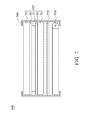
- FIG. 8 shows a schematic view of a conventional photo-alignment apparatus.
- FIG. 2 shows a side view showing the A-A section observed along the X direction in FIG. 1 in accordance with the exemplary embodiment of the present invention, wherein only one exposure machine 100 and partial masks 200 which are set in a first photo-alignment area E 1 are shown in FIG. 2 for simplification.
- the photo-alignment apparatus 50 includes a conveying track 60 , a plurality of exposure machines 100 , and a plurality of masks 200 .
- the conveying track 60 includes a conveying belt 62 , a frame body 64 , and a photo-alignment area E, wherein the conveying belt 62 is capable of conveying a plurality of large-sized substrates having 2500 millimeter in width along a manufacturing direction (X-direction).
- the frame body 64 corresponds to a portion of conveying belt 62 and is disposed thereabove for allowing the exposure machine 100 and the masks 200 to be installed therein.
- the photo-alignment area E is defined at an area of the surface of the conveying belt 62 which is below the exposure machine 100 and the masks 200 . Being conveyed along the manufacturing direction (X-direction), the substrates 70 pass through a first photo-alignment area E 1 and a second photo-alignment area E 2 orderly.
- the photo-alignment apparatus 50 includes eleven exposure machines 100 , wherein six of the exposure machines 100 are corresponding to the first photo-alignment area E 1 and disposed inside the frame body 64 , and the other 5 exposure machines 100 are corresponding to the second photo-alignment area E 2 and disposed inside the frame body 64 .
- the exposure machines 100 in the first photo-alignment area E 1 are disposed inside the frame body 64 along a predetermined direction (Y-direction), wherein the exposure machines 100 are spaced apart from one another by a space S, and the exposure machines 100 in the second photo-alignment area E 2 respectively corresponds to one of the spaces S and are disposed inside the frame body 64 along a predetermined direction (Y-direction).
- the number of the exposure machines 100 can be changed as desired.
- the number of the exposure machines 100 can be changed according to the number of the substrates simultaneously exposed thereto or the specification of the photo-alignment apparatus 50 .
- each of the exposures 100 includes a light source 110 , a reflective plate 120 , a polarization plate 130 , a multilayer splitter 140 , and two light transport plates 150 and 155 .
- the light source 110 includes a lamp 113 and a reflective cover 115 .
- the lamp 113 is configured to irradiate unpolarized light UV (such as ultraviolet light in the embodiment).
- the reflective cover 115 is configured to reflect or to converge the unpolarized light UV emitted from the lamp 113 to the reflective plate 120 .
- the light source 110 of the exposure machine 100 is a unitary light source.
- unitary should not be narrowly construed as being limited to the number of light source 110 or light emitting elements inside the light source 110 , but “unitary” should be broadly defined as the traveling direction of the light produced by the light source 110 .
- the arrow shown in FIG. 3 indicates that the unpolarized light UV from the light source 110 is generally projected to the reflective plate 120 along a unitary direction.
- the reflective plate 120 is configured to reflect the unpolarized light UV emitted from the light source 110 toward to the polarization plate 130 .
- the polarization plate 130 receives the unpolarized light UV and converts the unpolarized light UV to a polarized light, in which the polarized light includes an S-polarized light UVS and a P-polarized light UVP.
- the polarization plate 130 is stacked by a plurality of layers which have different index of refractions, while the light from the reflective plate 120 is projected into the polarization plate 130 at a particular angle, such as a Brewster angle, the S-polarized light UVS is totally reflected by the polarization plate 130 , and the P-polarized light UVP is able to pass through the polarization plate 130 .
- the P-polarized light UVP from the polarization plate 130 is projected to the multilayer splitter 140 , the P-polarized light UVP is equally split into a first light beam LB 1 and a second light beam LB 2 , wherein the first light beam LB 1 is reflected by the multilayer splitter 140 , and the second light beam LB 2 passes through the multilayer splitter 140 .
- the two light transport plates 150 and 155 are disposed at two opposite sides of the multilayer splitter 140 to reflect the first light beam LB 1 and the second light beam LB 2 , respectively.
- the arranged angles of the two light transport plates 150 and 155 can be adjusted as desired to change the traveling direction of the first light beam LB 1 and the second light beam LB 2 , so that the first light beam LB 1 and the second light beam LB 2 can be guided to the photo-alignment area E on the conveying track 60 at a particular angle.
- the arranged angles and positions of the two light transport plates 150 and 155 can be adjusted according to the shape of the masks 200 , the arranged angle of the masks 200 , or the desired light traveling path.
- Each of the masks 200 respectively includes a first mask part 210 , a second mask part 220 , and a holder 230 .
- the holders 230 are connected to the frame body 64 , so that the first and second mask parts 210 and 220 are disposed between the exposure machine 100 and the conveying track 60 .
- the first mask part 210 extends along the predetermined direction (Y-direction) and includes a plurality of exposure units 211 consecutively arranged in the predetermined direction (Y-direction).
- Each of the plurality of exposure units 211 respectively includes a transmission portion 213 to allow light to pass therethrough and a blocking portion 215 to block light, wherein the transmission portion 213 and the blocking portion 215 are arranged in the predetermined direction (Y-direction) orderly.
- the transmission portion 213 and the blocking portion 215 are arranged alternatively on the first mask part 210 .
- each of the plurality of exposure units 211 has a length d 1 .
- Each of the transmission portions 213 and each of the blocking portions 215 has a length d 2 and a length d 3 in the predetermined direction (Y-direction) and has a width H 1 in the manufacturing direction (X-direction).
- the size of the width H 1 is determined by the summation of the desired exposure energy, which will be described in detail later.
- each of exposure units 211 may have two or more than two transmission portions 213 and two or more than two blocking portions 215 , wherein the number of the transmission portions 213 and the number of the blocking portions 215 may be different.
- each of the plurality of exposure units 211 has two transmission portions 213 and two blocking portions 215 , wherein the transmission portions 213 and the blocking portions 215 are alternatively arranged on the first mask part 210 , and each of the transmission portions 213 has a length d 2 , and the blocking portions 215 has a length d 3 .
- the second mask part 220 has a plurality of exposure units 221 and each of the plurality of exposure units 221 respectively has a transmission portion 223 and a blocking portion 225 .
- the description of the plurality of exposure units 221 on the second mask part 220 is omitted here since it is similar to the plurality of exposure units 211 of the first mask part 210 for simplification. It is noted that, however, in the manufacturing direction (X-direction), the transmission portion 223 of the exposure unit 221 and the blocking portion 215 of the exposure unit 215 may be arranged in the same line. That is, they are overlapped to each other in the manufacturing direction (X-direction). In addition, the exposure portions 223 and the blocking portions 225 of each of the plurality of exposure units have a width H 2 .
- FIG. 6 shows the flowchart describing an exemplary embodiment of a method of manufacturing an alignment layer.
- a photosensitive material 80 is applied on the substrate 70 ( FIG. 1 , S 10 ), wherein the photosensitive material 80 is applied on the surface which will be inject liquid crystal molecules later.
- a light source 110 is provided to produce an unpolarized light UV ( FIG. 3 , S 20 ), and a polarization plate 130 is provided to split the unpolarized light UV into an S-polarized light UVS and a P-polarized light UVP ( FIG. 3 , S 30 ).
- a multilayer splitter 140 is provided to split the P-polarized light UVP into a first light beam LB 1 and a second light beam LB 2 ( FIG. 3 , S 40 ). Last, the photosensitive material 80 is projected by the first light beam LB 1 and the second light beam LB 2 ( FIG. 3 , S 50 ).
- FIG. 5 shows a schematic view illustrating a process of photo-aligning on the alignment layer.
- the substrate 70 has a first sub-pixel area SP 1 and a second sub-pixel area SP 2 adjacent to the first sub-pixel area SP 1 .
- the first light beam LB 1 passing through the transmission portion 213 of the first mask part 210 , is projected on the first sub-pixel area SP 1 of the substrate 70 , such that a first photo-alignment direction a 1 is formed on the surface of the first sub-pixel area SP 1 .
- the second light beam LB 2 passing through the transmission portion 223 of the second mask part 220 , is projected on the second sub-pixel area SP 2 of the substrate 70 , such that a second photo-alignment direction a 2 is formed on the surface of the second sub-pixel area SP 2 .
- the first light beam LB 1 is projected on the photosensitive material 80 at a first incident angle ⁇ 1 relative to the manufacturing direction (X-direction)
- the second light beam LB 2 is projected on the photosensitive material 80 at a second incident angle ⁇ 2 relative to the manufacturing direction (X-direction)
- the photosensitive material (alignment layer) 80 exposed to the first light beam LB 1 and the second light beam LB 2 includes two substantially opposite photo-alignment directions a 1 and a 2 .
- the photosensitive material 80 is exposed to the first light beam LB 1 and the second light beam LB 2 which is split from a unitary P-polarized light UVP, a different energy intensity between the first light beam LB 1 and the second light beam LB 2 may occur.
- the traveling path of the first light beam LB 1 and the second light beam LB 2 prior to their approaching on the substrate 70 , may be adjusted to be substantially equal. Specifically, after passing through the multilayer splitter 140 , the first light beam LB 1 along a first traveling path consecutively passes through the light transport plate 150 and the transmission portion 213 of the first mask part 210 and is projected to the photosensitive material 80 .
- the second light beam LB 2 along a second traveling path consecutively passes through the light transport plate 155 and the transmission portion 223 of the second mask part 220 and is projected to the photosensitive material 80 .
- the first traveling path may be as same as the second traveling path.
- the first traveling path may be different from the second traveling path, but the arranged position of the masks 200 or arranged angle of the masks 200 or the shape of the masks 200 may be corporately adjusted to meet the requirement of a photo-alignment process.
- the width H 1 of the transmission portion 213 and the width H 2 of the transmission portion 223 can be correspondingly modified by a designer.
- the width H 1 may be larger than the width H 2 , so that the first sub-pixel area SP 1 and the second sub-pixel area SP 2 may receive substantially equivalent summation of the exposure energy.
- the summation of the exposure energy projected on the photosensitive material 80 by the first light beam LB 1 and the second light beam LB 2 may be changed.
- FIG. 7 shows an exploded view of elements of the liquid crystal display device 500 of the exemplary embodiment of the present invention.
- the liquid crystal display device 500 includes a liquid crystal panel 510 , at least one optical film 520 , a backlight module 530 , and a frame 540 .
- the at least one optical film 520 is disposed above the backlight module 530 .
- the liquid crystal panel 510 is disposed above the at least one optical film 520 and includes two base plates 70 and a liquid crystal layer 75 , wherein the two base plates 70 are configured with two photo-aligned alignment layers 80 .
- the frame 540 surrounds the liquid crystal panel 510 , the at least one optical film 520 and the backlight module 530 to fix all of them therein.
- the liquid crystal layer 75 is firstly disposed on a side of the base plate 70 which is configured with the alignment layer 80 .
- a side of another substrate 70 which is configured with the alignment layer 80 is disposed on the liquid crystal layer 75 so that the liquid crystal layer 75 is sandwiched between the two substrates 70 .
- the two substrates 70 are bounded together to form the liquid crystal panel 510 .
- the at least one optical film 520 and the backlight module 530 are provided to be adjacently disposed on the light incident surface of the liquid crystal panel 510 .
- the frame 540 is provided to fix the liquid crystal panel 510 , the at least one optical film 520 , and the backlight module 530 therein.
- the photo-alignment apparatus of the alignment layer of the present invention is able to simultaneously form two different alignment directions by a unitary light source, which may reduce manufacturing time, and the installed floor area of the plant, so that the manufacturing cost can be reduced.
Landscapes
- Physics & Mathematics (AREA)
- General Physics & Mathematics (AREA)
- Nonlinear Science (AREA)
- Spectroscopy & Molecular Physics (AREA)
- Mathematical Physics (AREA)
- Chemical & Material Sciences (AREA)
- Crystallography & Structural Chemistry (AREA)
- Optics & Photonics (AREA)
- Engineering & Computer Science (AREA)
- Manufacturing & Machinery (AREA)
- Liquid Crystal (AREA)
- Exposure And Positioning Against Photoresist Photosensitive Materials (AREA)
Abstract
Description
Claims (8)
Applications Claiming Priority (3)
| Application Number | Priority Date | Filing Date | Title |
|---|---|---|---|
| TW100135465A TW201314374A (en) | 2011-09-30 | 2011-09-30 | Apparatus for photoalingment, and method for forming alignment layer, and method for fabricating liquid crystal display |
| TW100135465 | 2011-09-30 | ||
| TW100135465A | 2011-09-30 |
Publications (2)
| Publication Number | Publication Date |
|---|---|
| US20130083307A1 US20130083307A1 (en) | 2013-04-04 |
| US8922757B2 true US8922757B2 (en) | 2014-12-30 |
Family
ID=47992294
Family Applications (1)
| Application Number | Title | Priority Date | Filing Date |
|---|---|---|---|
| US13/592,823 Active 2033-02-08 US8922757B2 (en) | 2011-09-30 | 2012-08-23 | Photo-alingment apparatus, and method for fabricating liquid crystal display |
Country Status (3)
| Country | Link |
|---|---|
| US (1) | US8922757B2 (en) |
| JP (1) | JP2013080215A (en) |
| TW (1) | TW201314374A (en) |
Cited By (2)
| Publication number | Priority date | Publication date | Assignee | Title |
|---|---|---|---|---|
| US20170139093A1 (en) * | 2014-04-03 | 2017-05-18 | Rolic Ag | Optical devices with patterned anisotropy incorporating parallax optic |
| WO2020186123A1 (en) * | 2019-03-13 | 2020-09-17 | Kent State University | Liquid crystal pancharatnam-berry phase optical elements and method of making the same |
Families Citing this family (5)
| Publication number | Priority date | Publication date | Assignee | Title |
|---|---|---|---|---|
| JP2014006364A (en) * | 2012-06-22 | 2014-01-16 | Toppan Printing Co Ltd | Exposure device and exposure method |
| JP5734494B1 (en) * | 2014-05-29 | 2015-06-17 | 株式会社飯沼ゲージ製作所 | Photo-alignment processing equipment |
| US12044933B2 (en) | 2015-08-07 | 2024-07-23 | Kent State University | Photopatterning of molecular orientations |
| JP2018120106A (en) * | 2017-01-26 | 2018-08-02 | 株式会社ブイ・テクノロジー | Polarized light irradiation apparatus and polarized light irradiation method |
| CN108761858B (en) * | 2018-05-21 | 2020-11-27 | 南京中电熊猫液晶显示科技有限公司 | Mask and method for recycling defective liquid crystal panel |
Citations (9)
| Publication number | Priority date | Publication date | Assignee | Title |
|---|---|---|---|---|
| US6206527B1 (en) * | 1998-11-24 | 2001-03-27 | Ushiodenki Kabushiki Kaisha | Device for oblique light irradiation |
| US20010041380A1 (en) * | 1999-08-31 | 2001-11-15 | Mahesh Govind Samant | Method for forming a multi-domain alignment layer for a liquid crystal display device |
| US20100035190A1 (en) | 2008-08-06 | 2010-02-11 | Samsung Electronics Co., Ltd. | Method of forming an alignment layer, and apparatus for forming the alignment layer |
| US20110141406A1 (en) | 2009-12-14 | 2011-06-16 | Industrial Technology Research Institute | Low color variation optical devices and backlight modules and liquid crysal displays comprising the optical devices |
| WO2011132620A1 (en) * | 2010-04-23 | 2011-10-27 | 株式会社ブイ・テクノロジー | Orientation treatment method and orientation treatment device |
| US20130003033A1 (en) * | 2011-06-29 | 2013-01-03 | Samsung Electronics Co., Ltd. | Exposure device, photo-mask, and method for manufacturing liquid crystal display |
| US20130169917A1 (en) * | 2010-09-17 | 2013-07-04 | V Technology Co., Ltd. | Exposure device |
| US20130230799A1 (en) * | 2010-11-10 | 2013-09-05 | Toshinari ARAI | Film exposure method |
| US20130235362A1 (en) * | 2010-11-08 | 2013-09-12 | V Technology Co., Ltd. | Exposure apparatus |
-
2011
- 2011-09-30 TW TW100135465A patent/TW201314374A/en unknown
-
2012
- 2012-08-23 US US13/592,823 patent/US8922757B2/en active Active
- 2012-09-10 JP JP2012198354A patent/JP2013080215A/en active Pending
Patent Citations (11)
| Publication number | Priority date | Publication date | Assignee | Title |
|---|---|---|---|---|
| US6206527B1 (en) * | 1998-11-24 | 2001-03-27 | Ushiodenki Kabushiki Kaisha | Device for oblique light irradiation |
| US20010041380A1 (en) * | 1999-08-31 | 2001-11-15 | Mahesh Govind Samant | Method for forming a multi-domain alignment layer for a liquid crystal display device |
| US20100035190A1 (en) | 2008-08-06 | 2010-02-11 | Samsung Electronics Co., Ltd. | Method of forming an alignment layer, and apparatus for forming the alignment layer |
| US20110141406A1 (en) | 2009-12-14 | 2011-06-16 | Industrial Technology Research Institute | Low color variation optical devices and backlight modules and liquid crysal displays comprising the optical devices |
| TW201120491A (en) | 2009-12-14 | 2011-06-16 | Ind Tech Res Inst | Low color variation optical devices and backlight modules and liquid crystal displays comprising the optical devices |
| WO2011132620A1 (en) * | 2010-04-23 | 2011-10-27 | 株式会社ブイ・テクノロジー | Orientation treatment method and orientation treatment device |
| US20130100431A1 (en) * | 2010-04-23 | 2013-04-25 | V Technology Co., Ltd. | Method and apparatus for alignment processing |
| US20130169917A1 (en) * | 2010-09-17 | 2013-07-04 | V Technology Co., Ltd. | Exposure device |
| US20130235362A1 (en) * | 2010-11-08 | 2013-09-12 | V Technology Co., Ltd. | Exposure apparatus |
| US20130230799A1 (en) * | 2010-11-10 | 2013-09-05 | Toshinari ARAI | Film exposure method |
| US20130003033A1 (en) * | 2011-06-29 | 2013-01-03 | Samsung Electronics Co., Ltd. | Exposure device, photo-mask, and method for manufacturing liquid crystal display |
Non-Patent Citations (2)
| Title |
|---|
| English language translation of abstract of TW 201120491 (published Jun. 16, 2011). |
| Taiwanese language office action dated Jan. 15, 2014. |
Cited By (3)
| Publication number | Priority date | Publication date | Assignee | Title |
|---|---|---|---|---|
| US20170139093A1 (en) * | 2014-04-03 | 2017-05-18 | Rolic Ag | Optical devices with patterned anisotropy incorporating parallax optic |
| US10845520B2 (en) * | 2014-04-03 | 2020-11-24 | Rolic Ag | Optical devices with patterned anisotropy incorporating parallax optic |
| WO2020186123A1 (en) * | 2019-03-13 | 2020-09-17 | Kent State University | Liquid crystal pancharatnam-berry phase optical elements and method of making the same |
Also Published As
| Publication number | Publication date |
|---|---|
| TW201314374A (en) | 2013-04-01 |
| US20130083307A1 (en) | 2013-04-04 |
| JP2013080215A (en) | 2013-05-02 |
Similar Documents
| Publication | Publication Date | Title |
|---|---|---|
| US8922757B2 (en) | Photo-alingment apparatus, and method for fabricating liquid crystal display | |
| CN103210344B (en) | Exposure device | |
| JP5704591B2 (en) | Alignment processing method and alignment processing apparatus | |
| US20130039030A1 (en) | Light irradiation apparatus | |
| KR101829778B1 (en) | Exposure device and manufacturing method of liquid crystal display | |
| CN103033988A (en) | Optical alignment device of alignment film and manufacturing method of alignment film | |
| TWI681263B (en) | Exposure method and device manufacturing method | |
| TWI521258B (en) | Light alignment illumination device | |
| JP2008164729A (en) | Light irradiator, light irradiator and exposure method | |
| KR20000057752A (en) | Polarized light illuminating apparatus for light orientation of liquid crystal device | |
| JP2012078697A (en) | Alignment layer exposure method for liquid crystal, its device and liquid crystal panel produced by applying the method | |
| KR20130128432A (en) | Orientation processing device and orientation processing method | |
| JP2011053584A (en) | Light irradiating device | |
| KR100865978B1 (en) | Light orientation method | |
| JP2015106015A (en) | Polarized light irradiation device, polarized light irradiation method and polarized light irradiation program | |
| JP6154750B2 (en) | Manufacturing method of optical film | |
| CN108521795B (en) | Apparatus and method for manufacturing display substrate of liquid crystal display panel | |
| KR20050039564A (en) | A polarized light illuminating apparatus used for light orientation and method for regulating the polarization axis of the same | |
| US9316923B2 (en) | Exposure apparatus and exposure method using the same | |
| KR20190139204A (en) | Light irradiation device | |
| WO2012046541A1 (en) | Exposure apparatus | |
| JP7573279B2 (en) | Polarized light irradiation device, exposure device including the same, and polarized light irradiation method | |
| KR20120032426A (en) | Light irradiation apparatus and light irradiation method | |
| TWM623150U (en) | Exposure apparatus | |
| JP2014006364A (en) | Exposure device and exposure method |
Legal Events
| Date | Code | Title | Description |
|---|---|---|---|
| AS | Assignment |
Owner name: INNOCOM TECHNOLOGY(SHENZHEN) CO., LTD., CHINA Free format text: ASSIGNMENT OF ASSIGNORS INTEREST;ASSIGNORS:TSENG, HUNG-I;KAO, KER-YIH;REEL/FRAME:028836/0805 Effective date: 20120715 Owner name: CHIMEI INNOLUX CORPORATION, TAIWAN Free format text: ASSIGNMENT OF ASSIGNORS INTEREST;ASSIGNORS:TSENG, HUNG-I;KAO, KER-YIH;REEL/FRAME:028836/0805 Effective date: 20120715 |
|
| AS | Assignment |
Owner name: INNOLUX CORPORATION, TAIWAN Free format text: CHANGE OF NAME;ASSIGNOR:CHIMEI INNOLUX CORPORATION;REEL/FRAME:032672/0813 Effective date: 20121219 |
|
| STCF | Information on status: patent grant |
Free format text: PATENTED CASE |
|
| MAFP | Maintenance fee payment |
Free format text: PAYMENT OF MAINTENANCE FEE, 4TH YEAR, LARGE ENTITY (ORIGINAL EVENT CODE: M1551) Year of fee payment: 4 |
|
| MAFP | Maintenance fee payment |
Free format text: PAYMENT OF MAINTENANCE FEE, 8TH YEAR, LARGE ENTITY (ORIGINAL EVENT CODE: M1552); ENTITY STATUS OF PATENT OWNER: LARGE ENTITY Year of fee payment: 8 |