US8856498B2 - Prefetch request circuit - Google Patents
Prefetch request circuit Download PDFInfo
- Publication number
- US8856498B2 US8856498B2 US13/220,006 US201113220006A US8856498B2 US 8856498 B2 US8856498 B2 US 8856498B2 US 201113220006 A US201113220006 A US 201113220006A US 8856498 B2 US8856498 B2 US 8856498B2
- Authority
- US
- United States
- Prior art keywords
- instruction
- memory
- prefetch
- memory copy
- prefetch request
- Prior art date
- Legal status (The legal status is an assumption and is not a legal conclusion. Google has not performed a legal analysis and makes no representation as to the accuracy of the status listed.)
- Expired - Fee Related, expires
Links
- 238000000034 method Methods 0.000 description 24
- 230000008569 process Effects 0.000 description 24
- 238000010586 diagram Methods 0.000 description 12
- 230000000694 effects Effects 0.000 description 5
- 102100029091 Exportin-2 Human genes 0.000 description 2
- 101000770958 Homo sapiens Exportin-2 Proteins 0.000 description 2
- 230000007246 mechanism Effects 0.000 description 2
- 230000004075 alteration Effects 0.000 description 1
- 230000007423 decrease Effects 0.000 description 1
- 230000003111 delayed effect Effects 0.000 description 1
- 230000008520 organization Effects 0.000 description 1
- 238000006467 substitution reaction Methods 0.000 description 1
Images


Classifications
-
- G—PHYSICS
- G06—COMPUTING; CALCULATING OR COUNTING
- G06F—ELECTRIC DIGITAL DATA PROCESSING
- G06F12/00—Accessing, addressing or allocating within memory systems or architectures
- G06F12/02—Addressing or allocation; Relocation
- G06F12/08—Addressing or allocation; Relocation in hierarchically structured memory systems, e.g. virtual memory systems
- G06F12/0802—Addressing of a memory level in which the access to the desired data or data block requires associative addressing means, e.g. caches
- G06F12/0862—Addressing of a memory level in which the access to the desired data or data block requires associative addressing means, e.g. caches with prefetch
-
- G—PHYSICS
- G06—COMPUTING; CALCULATING OR COUNTING
- G06F—ELECTRIC DIGITAL DATA PROCESSING
- G06F9/00—Arrangements for program control, e.g. control units
- G06F9/06—Arrangements for program control, e.g. control units using stored programs, i.e. using an internal store of processing equipment to receive or retain programs
- G06F9/30—Arrangements for executing machine instructions, e.g. instruction decode
- G06F9/30003—Arrangements for executing specific machine instructions
- G06F9/3004—Arrangements for executing specific machine instructions to perform operations on memory
- G06F9/30043—LOAD or STORE instructions; Clear instruction
-
- G—PHYSICS
- G06—COMPUTING; CALCULATING OR COUNTING
- G06F—ELECTRIC DIGITAL DATA PROCESSING
- G06F9/00—Arrangements for program control, e.g. control units
- G06F9/06—Arrangements for program control, e.g. control units using stored programs, i.e. using an internal store of processing equipment to receive or retain programs
- G06F9/30—Arrangements for executing machine instructions, e.g. instruction decode
- G06F9/3017—Runtime instruction translation, e.g. macros
-
- G—PHYSICS
- G06—COMPUTING; CALCULATING OR COUNTING
- G06F—ELECTRIC DIGITAL DATA PROCESSING
- G06F9/00—Arrangements for program control, e.g. control units
- G06F9/06—Arrangements for program control, e.g. control units using stored programs, i.e. using an internal store of processing equipment to receive or retain programs
- G06F9/30—Arrangements for executing machine instructions, e.g. instruction decode
- G06F9/30181—Instruction operation extension or modification
-
- G—PHYSICS
- G06—COMPUTING; CALCULATING OR COUNTING
- G06F—ELECTRIC DIGITAL DATA PROCESSING
- G06F9/00—Arrangements for program control, e.g. control units
- G06F9/06—Arrangements for program control, e.g. control units using stored programs, i.e. using an internal store of processing equipment to receive or retain programs
- G06F9/30—Arrangements for executing machine instructions, e.g. instruction decode
- G06F9/34—Addressing or accessing the instruction operand or the result ; Formation of operand address; Addressing modes
-
- G—PHYSICS
- G06—COMPUTING; CALCULATING OR COUNTING
- G06F—ELECTRIC DIGITAL DATA PROCESSING
- G06F9/00—Arrangements for program control, e.g. control units
- G06F9/06—Arrangements for program control, e.g. control units using stored programs, i.e. using an internal store of processing equipment to receive or retain programs
- G06F9/30—Arrangements for executing machine instructions, e.g. instruction decode
- G06F9/38—Concurrent instruction execution, e.g. pipeline or look ahead
- G06F9/3824—Operand accessing
- G06F9/383—Operand prefetching
Definitions
- the embodiments described in the application are related to a prefetch request circuit.
- a processor device of a computer is, generally, equipped with a secondary cache and a primary data cache, a primary instruction cache and the like to enhance the access performance to a main memory.
- an instruction read out from the main memory via the secondary cache and the primary instruction cache is sent to an instruction decoder and decoded.
- an operand address generator calculates the memory address to be accessed, and an access to the primary data cache is performed with the calculated address.
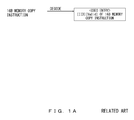
- a process illustrated in FIG. 1A is performed for example. That is, the decoded memory copy instruction is sequentially registered in the order of decoding in an instruction queue called CSE (Commit Stack Entry). In the example in FIG. 1A , it is assumed that the memory copy instruction is registered in an entry CSE 0 of the CSE.
- CSE Common Stack Entry
- an IID instruction identifier
- the number of entries of the CSE is for example about several dozen entries.
- the processor is equipped with, other than the CSE, an instruction queue called RS (Reservation Station) in which each instruction can be registered with priority and can be executed out-of-order.
- An IID to identify each instruction is also registered in each entry of the RS.
- the memory copy instruction is processed in the operand address generator via the RS, and a memory copy process according to the memory copy instruction is performed. In this case, the instruction registered in the CSE in the order of decoding and the instruction executed out-of-order via the RS are linked by the IID.
- the instruction for which execution is completed via the RS is compared with an entry in the CSE by the IID registered in the entry of the RS corresponding to the instruction, and the valid flag of the entry of the CSE in which the same IDD is registered is changed to a value indicating invalidity, to complete the execution of the instruction.
- the order of instructions executed out-of-order via the RS is ensured by the CSE according to the linked control.
- the data transfer capacity of a memory copy instruction is for example 16 bytes (16 B), and a “16 B memory copy” instruction indicates that it is a data transfer instruction up to 16 bytes.
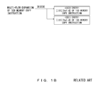
- a process illustrated in FIG. 1B is executed.
- the instruction decoder executes a process called multi-flow expansion for a “32 B memory copy” instruction that is a data transfer instruction for 32 bytes for example.
- the “32 B memory copy” instruction is separated into two “16 B memory copy” instructions.
- Each of the “16 B memory copy” instructions decoded into a plurality of instructions in this way is registered in an individual CSE entry CSE 0 and CSE 1 as illustrated in FIG. 1B .
- Each of the “16 B entry copy” instructions registered respectively in the CSE 0 and CSE 1 is executed out-of-order via an individual RS entry linked via corresponding IID registered together with each of the instructions, and is subjected individually to a pipeline process in the operand address generator. As a result, 16-byte memory copy process is executed.
- each memory copy instruction when it is desired to perform copy of data exceeding the maximum size that can be specified by a memory copy instruction, the memory copy instructions are described successively in the program. That is, a memory copy process for a large size is described as a plurality of successive memory copy instructions. Furthermore, when the data size specified by each memory copy instruction exceeds the data transfer capacity in one cycle between the secondary cache and the primary data cache, each memory copy instruction is subjected to multi-flow expansion and executed. For example, it is assumed that the data transfer capacity between the secondary cache and the primary data cache is 16 bytes, and the maximum data size specified by one memory copy instruction is 256 bytes. In this case, a memory copy process for 1024 bytes for example is described as four successive 256-byte memory copy instructions, and each of the 256-byte memory copy instructions are subjected to multi-flow expansion into 16 16-byte memory copy instructions.
- MF memory copy instruction the memory copy instruction obtained by performing multi-flow expansion for each memory copy instruction.
- a prefetch request is issued for the execution of the first MF memory copy instruction obtained by performing multi-flow expansion for each memory copy instruction.
- the prefetch instruction is not issued at the time of execution of the second and subsequent MF memory copy instructions obtained by performing multi-flow instruction for each memory copy instruction.
- memory data of an address range of several blocks from the memory address specified by the first MF memory copy instruction are fetched from the main memory to the secondary cache, and a part of the memory data is further fetched also to the primary data cache.
- the address range of several blocks is an address range corresponding for example to one data transfer from the main memory to the secondary cache, for example 256 bytes.
- the prefetch operation described above is not performed.
- the primary data cache is missed (L 1 $miss) at the time of executing the second and subsequent MF memory copy instructions, the normal fetch operation for the secondary cache or the main memory is performed.
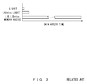
- the memory block of one data transfer from the second cache to the primary data cache is 64 bytes (64 B), and the maximum data size that can be specified with one memory copy instruction is 256 bytes.
- one large-size memory copy process is performed with successive 256-byte memory copy instructions. Then, assuming that each of the address A, B is located at the block boundary of the memory block, the copy source start address is A and the copy destination start address is B in the first 256-byte memory copy instruction in the memory copy process.
- a prefetch request is issued at the time of execution of the first MF memory copy instruction obtained by performing multi-flow expansion for the first (1st) memory copy instruction.
- the copy source start address is A
- the copy destination start address is B.
- the prefetch instruction is not issued for the second and subsequent MF copy instructions obtained by performing multi-flow expansion for the first (1st) memory copy instruction.
- copy source memory data of the address range of 4 memory blocks from the memory address A specified by the first MF memory copy instruction corresponding to the first (1st) memory copy instruction is fetched from the main memory to the secondary cache.
- a part of memory blocks in the memory data fetched to the secondary cache is also fetched to the primary data cache.
- the copy destination memory area of the address range (from B to B+255) corresponding to 4 memory blocks from the memory address B specified by the first MF memory copy instruction is reserved (fetched) in the secondary cache.
- a prefetch operation is performed. That is, copy source memory data of the address range corresponding to further 4 memory blocks from the 4 memory blocks from the memory address specified by the first MF copy instruction described above is prefetched from the main memory to the secondary cache.
- the address range is from A+256 to A+511. The same applies for reserving the area (prefetch) in the secondary cache for the copy destination memory data (from B+256 to B+511).
- the prefetch operation described above is not performed.
- the primary data cache is missed (L 1 $miss) at the time of executing the second and subsequent MF memory copy instructions
- the normal fetch operation is performed.
- a fetch operation for the address range corresponding to 4 memory blocks from the memory address A (or B) from the main memory to the secondary cache has been performed.
- the secondary cache is hit, realizing a high-speed memory access.
- the case in which after the first (1st) memory copy instruction is subjected to multi-flow expansion and executed, the second (2nd) memory copy instruction is executed successively is considered.
- the primary data cache is missed (L 1 $miss) for each MF memory copy instruction corresponding to the second (2nd) memory copy instruction
- memory data corresponding to each MF memory copy instruction mentioned above has been prefeched in the secondary cache. That is to say, the secondary cache is hit. Accordingly, control so as to reduce penalty due to miss of the secondary cache (L 2 $miss) for the second (2nd) memory copy instruction is performed.
- a prefetch request is issued again, Therefore, if the primary data cache is missed (L 1 $miss) at the time of execution of the first MF memory copy instruction corresponding to the second (2nd) memory copy instruction, a prefetch operation for the third (3rd) memory copy instruction is performed based on the prefetch request. Accordingly, a prefetch operation from the main memory of the address range from A+512 to A+767 and from B+512 to B+767 to the secondary cache is to be performed.
- the prefetch operation for the next memory copy instruction of the memory copy instruction being currently performed is performed sequentially.
- the memory block of one data transfer from the second cache to the primary data cache is 64 bytes (64 B), and the maximum data size that can be specified with one memory copy instruction is 256 bytes.
- one large-size memory copy process is performed with successive 256-byte memory copy instructions.
- the copy source start address is A+16
- the copy destination start address is B+16 in the first 256-byte memory copy instruction in the memory copy process. That is, while in the case 1 in FIG. 2 , the start address of the memory copy process is located on the block boundary (address A, B), in the case 2 in FIG. 4 , the start address is not located on the block boundary.
- a prefetch request is issued at the time of execution of the first MF memory copy instruction obtained by performing multi-flow expansion for the first (1st) memory copy instruction.
- the copy source start address is A+16
- the copy destination start address is B+16.
- the prefetch instruction is not issued for the second and subsequent MF copy instructions obtained by performing multi-flow expansion for the first (1st) memory copy instruction, similar to the case 1 in FIG. 3 .
- copy source memory data of the address range of 4 memory blocks from the memory address A+16 specified by the first MF memory copy instruction corresponding to the first (1st) memory copy instruction is fetched from the main memory to the secondary cache.
- a part of memory blocks in the memory data fetched to the secondary cache is also fetched to the primary data cache. The same applies to reservation (fetch) of the areas in the secondary cache for the copy destination memory data (from B to B+255).
- a prefetch operation is performed. That is, copy source memory data of the address range corresponding to further 4 memory blocks from the 4 memory blocks from the memory address specified by the first MF copy instruction described above is prefetched from the main memory to the secondary cache.
- the address range is also specified in units of memory blocks, and is from A+256 to A+511. The same applies for the reservation of the area (prefetch) in the secondary cache for the copy destination memory data (from B+256 to B+511).
- the copy source start address is A+272
- the copy destination start address is B+272.
- the memory block in which these addresses are included is the same one as the memory block that was accessed when the last MF memory copy instruction corresponding to the first (1st) memory copy instruction was executed. Therefore, in the case 2 in FIG. 4 , at the time of executing the first MF memory copy instruction corresponding to the second (2nd) memory copy instruction, the primary data cache is hit (L 1 $HIT) without being missed.
- the prefetch operation from the main memory to the secondary cache is performed only when a prefetch request has been issued to the primary data cache and the primary data cache is missed (L 1 $miss). Therefore, at the time of execution of the first MF memory copy instruction corresponding to the second (2nd) memory copy instruction, although a prefetch request has been issued, a prefetch operation for the third (3rd) memory copy instruction is not to be performed.
- the copy source start address is A+528, and the copy destination start address is B+528.
- the memory block in which these addresses are included is the same one as the memory block that was accessed when the last MF memory copy instruction corresponding to the second (2nd) memory copy instruction was executed. Therefore, in the case 2 in FIG. 4 , at the time of executing the first MF memory copy instruction corresponding to the second (3nd) memory copy instruction, the primary data cache is also hit (L 1 $HIT) without being missed. For this reason, also at the time of execution of the first MF memory copy instruction corresponding to the third (3rd) memory copy instruction, although a prefetch request has been issued, a prefetch operation for the fourth (4th) memory copy instruction is not to be performed.
- a prefetch request circuit is provided in a processor device, the processor device having hierarchized two or more storage areas, the processor device being able to prefetch data of address to be used between appropriate storage areas among the two or more storage areas, when executing respective instruction flows obtained by multi-flow expansion for one instruction at a time of decoding of the instruction.
- the prefetch request circuit includes: a latch unit to hold, when a state in which the respective instruction flows to access the storage area are executed with a maximum specifiable data transfer volume is specified, the state during a time period of the multi-flow expansion; and a prefetch request signal output unit to output a prefetch request signal to request the prefetch every time when the instruction flow is executed, based on an output signal of the latch unit and a signal indicating an execution timing of the respective instruction flows.
- FIG. 1A and FIG. 1B are explanatory diagrams of multi-flow expansion.
- FIG. 2 is an explanatory diagram of penalty at the time of cache miss.
- FIG. 3 is a diagram for explaining the effect of prefetch.
- FIG. 4 is an explanatory diagram of a problem with conventional arts.
- FIG. 5 is an overall configuration diagram of a processor device to which the embodiment may be applied.
- FIG. 6 is an explanatory diagram of a memory access operation by the instruction decoder, CSE, RSA, operand address generator, and primary data cache in FIG. 5 .
- FIG. 7 is a diagram illustrating an embodiment of a prefetch request circuit.
- FIG. 8 is an operation timing chart of an embodiment of the prefetch request circuit.
- FIG. 9 is a diagram explaining the effect of the embodiment.
- FIG. 5 is an overall configuration diagram of a processor device according to an embodiment of the present invention.
- a necessary instruction is read out from a main memory 501 via a secondary cache 502 and the primary instruction cache 503 .
- the read out instruction is sent to an instruction decoder 504 .
- the instruction decoder 504 decodes an instruction in order in a decode (D) cycle.
- Instructions decoded by the instruction decoder 504 are registered in order in a CSE (commit Stack Entry) 505 .
- instructions decoded by the instruction decoder 504 are registered in an RSA (Reservation Station for Address) 506 and an RSE (Reservation Station for Execute) 507 to perform out-of-order execution control.
- the instruction decoded by the instruction decoder 504 is a branch instruction, the instruction is registered in an RSBR (Reservation Station for Branch) 508 .
- an IID instruction identifier
- a valid flag for specifying whether the registered instruction is valid or invalid is registered together with the IID.
- the instructions registered in the CSE 505 in the order of decoding and the instructions executed out of order via the RSA 506 , the RSE 507 or the RSBR 508 are linked by the instruction identifier (IID).
- the instruction for which execution is completed via the RSA 506 , the RSE 507 or the RSBR 508 is compared with the entry in the CSE 505 using the IID registered in the entry of the RSA 506 , the RSE 507 or the RSBR 508 corresponding to the instruction. Then, the valid flag of the entry in the CSE 505 in which the same IID is registered is changed to a value indicating invalidity and the execution of the instruction is completed. According to this link control, the order of instructions executed out of order via the RSA 506 , the RSE 507 or the RSBR 508 are ensured by the CSE 505 .
- each instruction issued by the instruction decoder 504 is registered in the RSA 506 .
- a subsequent instruction issued by the instruction decoder 504 is registered in the RSA 506 .
- the priority of each entry is determined.
- an operand address generator 509 calculates the memory address to access in the address calculation (X) cycle.
- the memory access instruction there are a load instruction, store instruction, memory copy instruction, and the like.
- the operand address generator 509 accesses the primary data cache 510 with the calculated address.
- the instruction is not registered in the RSA 506 and fed to the operand address generator 509 immediately after being decoded by the instruction decoder 504 .
- a prefetch request signal +P_PREFETCH_REQUEST is issued.
- the prefetch request signal is issued only at a timing at which the first MF memory copy instruction among MF memory copy instructions (multi-flow expansion instruction) corresponding to the memory copy instruction having the maximum copy size is issued, as described in FIG. 3 or FIG. 4 etc.
- the prefetch request signal +P_PREFETCH_REQUEST is issued every time the MF memory copy instruction obtained by multi-flow expansion from the memory copy instruction having the maximum copy size is issued from the RSA 506 .
- arithmetic operation instruction or a logic operation instruction For an arithmetic operation instruction or a logic operation instruction, the contents of a fixed decimal point register 513 or a floating decimal point register 514 is read, and fed to an operator 511 or 512 out of order.
- the operator 511 or 512 executes an operation specified by the operation instruction in an operation execution (x) cycle.
- the execution result in the operator 511 or 512 is stored in the fixed decimal point update buffer 515 or the floating decimal point update buffer 516 in the register update (U) cycle, and waits for the instruction completion (commit) process.
- the CSE 505 receives a report of the operation execution completion in the operator 511 or 512 , the data transfer completion in the primary data cache 510 , or the branch judgment completion from a branch prediction mechanism 518 and the like, the commit process is performed in order in the fixed decimal point update buffer 515 or the floating decimal point update buffer 516 .
- the register write (W) cycle writing into register 513 or 514 from the fixed decimal point update buffer 515 or the floating decimal point update buffer 516 is performed.
- the instruction fetch address generator 519 generates the next instruction fetch address based on instruction fetch address information given from the PSW 517 , RSBR 508 , or RSBR 508 via the branch prediction mechanism 518 , and accesses the primary instruction cache 503 with the generated instruction fetch address.
- a memory block including the address to be accessed is fetched from the secondary cache 502 or the main memory 501 .
- data is provided to the primary data cache 510 .
- An instruction such as the memory copy instruction that cannot be processed in one pipeline is subjected to multi-flow expansion in the operation decoder 504 . Then, for every expanded flow, registration of instruction in the CSE 505 , RSA 506 , RSE 507 and RSBR 508 is performed, and one instruction is executed by superscalar and pipeline process.
- FIG. 6 is an explanatory diagram of a memory access operation by the instruction decoder 504 , CSE 505 , RSA 506 , operand address generator 509 , and primary data cache 510 .
- An MVC (MOVE character) instruction is assumed as an example of a memory copy instruction.
- the MVC instruction is a memory copy instruction to specify data of maximum 256 bytes in units of bytes and copy the data from any copy source address A to a copy destination address B.
- an MVC instruction of the maximum value 256 bytes is called an “MVC 256” instruction.
- an MVC 256 instruction decoded in a decode (D) cycle is separated into 16 “MVC 16” instructions by multi-flow expansion.
- the “MVC 16” instruction is an instruction to perform data LOAD or STORE, or simultaneous processing of LOAD and STORE for the main memory 501 , the secondary cache 502 , or the primary data cache 510 in units of 16 bytes.
- Each of the “MVC 16” instructions subjected to the multi-flow expansion and decoded into a plurality of MF memory copy instructions is registered individually in the CSE entries CSE 0 -CSE 15 of the CSE 505 , as illustrated in FIG. 6 .
- each of the “MVC 16” instructions is registered in the RSA 506 and RSE 507 .
- the IID of each of the “MVC 16” instructions is registered in each of the CSE entries CSE 0 -CSE 15 , and each of the CSE entries CSE 0 -CSE 15 and each entry in the RSA 506 of the RSE 507 are linked.
- +D_MVC — 256 — 1ST signal is set in the entry in the RSA 506 in which the first “MVC 16” instruction among the “MVC 16” instructions obtained by multi-flow expansion from the “MVC 256” instruction is registered, together with the IID corresponding to the first “MVC 16” instruction.
- the +D_MVC — 256 — 1ST signal set from the instruction decoder 504 , indicates the first MF memory copy instruction with multi-flow expansion for a memory copy instruction whose copy size is the maximum of 256 bytes.
- the +D_MF_TGR signal of high level is output from the instruction decoder 504 to the RSA 506 .
- Each entry of each “MVC 16” instruction registered in the RSA 506 is issued to the operand address generator 509 in descending order of priority. As a result, the operand address generator 509 performs memory access to the primary data cache 510 . Meanwhile, from the RSA 506 to the primary data cache, every time when each “MVC 16” instruction is issued, +P_EAG_VALID signal for enabling the operand address generator 509 (EAG) VALID is asserted.
- a prefetch request signal +P_PREFETCH_REQUEST is asserted.
- FIG. 7 is a diagram illustrating the configuration of a prefetch request circuit implemented in the RSA 506 to issue the prefetch request signal +P_PREFETCH_REQUEST mentioned above.
- FIG. 8 is an operation timing chart illustrating the operation of the prefetch request circuit in FIG. 7 .
- a prefetch request signal is issued only when the first “MVC 16” instruction is issued.
- the prefetch request signal +P_PREFETCH_REQUEST is issued every time when the “MVC 16” instruction is issued as illustrated as FIG. 8( i ).
- the prefetch request circuit in FIG. 7 operates as described below.
- the prefetch request circuit in FIG. 7 operates according to +D_MF_TGR signal, +P_EAG_VALID signal and +P_MVC — 256 — 1ST signal.
- the +D_MF_TGR signal is, as described above, issued by the instruction decoder 504 and is asserted in the time period during which multi-flow expansion is performed.
- the +D_MF_TGR signal is asserted in the time period from t 2 to t 5 in FIG. 8( d ).
- the +P_EAG_VALID signal is, as described above, asserted by the RSA 506 every time when the RSA 506 issues an instruction to the operand address generator 509 .
- the +P_EAG_VALID signal is asserted at each timing of t 1 , t 3 , t 4 in FIG. 8( a ).
- the +P_MVC — 256 — 1ST signal is generated within the RSA 506 based on the +D_MVC — 256 — 1ST signal issued by the instruction decoder 504 . More specifically, the +P_MVC — 256 — 1ST signal is issued at the timing when the first “MVC 16” instruction obtained by multi-flow expansion from the “MVC 256” instruction having the maximum copy size is issued from the RSA 506 to the operand address generator 509 .
- the +P_MVC — 256 — 1ST signal is asserted based on the +D_MVC — 256 — 1ST signal set in the entry in the RSA 506 in which the first “MVC 16” instruction is registered.
- the +P_MVC — 256 — 1ST signal is asserted at the timing t 1 in FIG. 8( b ) for example.
- an AND circuit 701 calculates AND operation between the +P_MVC — 256 — 1ST signal ( FIG. 8( b )) and the +P_EAG_VALID signal ( FIG. 8( a )), and outputs a signal that is asserted in the time period from t 1 to t 2 in FIG. 8( c ) for example.
- the output of the AND circuit 702 asserted in the time period from t 1 to t 2 is issued to the primary data cache 510 via an OR circuit 706 as a prefetch request signal +P_PREFETCH_REQUEST corresponding to the first multi-flow expansion instruction “MVC16” for the “MVC 256” instruction.
- FIG. 8( d ) illustrates the output signal of the OR circuit 702 input to Din, which is asserted in the time period from t 1 to t 5 .
- the signal latched by the 1-bit latch 703 is output from Dout of the 1-bit latch 703 in the next clock cycle.
- the Dout output signal is ANDed in an AND circuit 704 with a +D_MF_TGR signal ( FIG. 8 ( d )) input by the instruction decoder 504 .
- the output of the AND circuit 704 is asserted in the time period from t 2 to t 5 in FIG. 8( e ) for example.
- the output signal of the AND circuit 704 is provided to the input terminal Din of the 1-bit latch 703 .
- the output terminal Dout of the 1-bit latch 703 is in the assert state.
- FIG. 8( g ) illustrates the output signal from the output terminal Dout of the 1-bit latch 703 , which is maintained in ON in the time period from t 2 to t 6 .
- An AND circuit 705 ANDs +P_EAG_VALID and the output signal Dout ( FIG. 8( g )) of the 1-bit latch 703 .
- the +P_EAG_VALID signal is asserted, as illustrated in FIG. 8( a ), every time when the RSA 506 issues an instruction to the operand address generator 509 .
- the output signal Dout of the 1-bit latch 703 is, as illustrated in FIG. 8( g ), asserted during the multi-flow expansion period of the “MVC 256” having the maximum copy size.
- the output signal of the AND circuit 705 is, as illustrated in FIG. 8( h ), asserted at each timing t 3 and t 4 corresponding to the second and subsequent multi-flow expansion instructions “MVC16” corresponding to the “MVC 256” instruction having the maximum copy size.
- This output signal is issued to the primary data cache 510 as the prefetch request signal +P_PREFETCH_REQUEST via the OR circuit 706 .
- a prefetch request signal +P_PREFETCH_REQUEST is issued to the primary data cache 510 at every timing of execution of each “MVC 16” instruction corresponding to the “MVC 256” instruction.
- FIG. 9 is a diagram for explaining the effect of the prefetch request circuit in FIG. 7 .
- the memory block of one data transfer from the second cache to the primary data cache is 64 bytes (64 B), and the maximum data size that can be specified with one memory copy instruction is 256 bytes.
- one large-size memory copy process is performed with successive 256-byte memory copy instructions.
- the copy source start address is A+16 and the copy destination start address is B+16 in the first 256-byte memory copy instruction in the memory copy process. That is, the start address of the memory copy process does not exist on the block boundary.
- a prefetch request signal +P_PREFETCH_REQUEST is issued by the prefetch request circuit in FIG. 7 at the time of execution of the first MF memory copy instruction obtained by performing multi-flow expansion for the first (1st) memory copy instruction.
- This timing corresponds for example to the time period from t 1 to t 2 in FIG. 8( i ).
- the copy source start address is A+16
- the copy destination start address is B+16.
- the operand address generator 509 calculates the access address, and accesses the primary data cache 510 .
- the primary data cache 510 and the secondary cache 502 are both missed (L 1 $, L 2 $miss) at the time of executing the first MF memory copy instruction corresponding to the first (1st) memory copy instruction, a fetch operation and a prefetch operation as described below are performed.
- copy source memory data of the address range of 4 memory blocks starting from the memory address A+16 specified by the first MF memory copy instruction corresponding to the first (1st) memory copy instruction is fetched from the main memory 501 to the secondary cache 502 .
- a part of memory blocks in the memory data fetched to the secondary cache 502 is also fetched to the primary data cache 510 .
- the similar process is applied to the reservation (fetch) of the areas in the secondary cache for the copy destination memory data (from B to B+255).
- a prefetch operation is performed. That is, copy source memory data of the address range of 4 memory blocks starting from an address forwarded 4 memory blocks from the memory address specified by the first MF memory copy instruction described above is prefetched from the main memory 501 to the secondary cache 502 .
- the address range is also specified in units of memory blocks, and is from A+256 to A+511. The similar process is applied to the reservation of the area (prefetch) in the secondary cache for the copy destination memory data (from B+256 to B+511).
- the prefetch request signal +P_PREFETCH_REQUEST is issued.
- the +P_PREFETCH_REQUEST is issued at the timing t 3 and timing t 4 in FIG. 8( i ).
- the primary data cache is missed (L 1 $miss)
- a prefetch operation is performed based on the prefetch request signal +P_PREFETCH_REQUEST issued for the MF memory copy instruction currently being executed.
- the portion that does not exist in the secondary cache 502 in the address range of 4 memory blocks starting from an address forwarded 4 memory blocks from the memory address specified by the MF memory copy instruction currently being performed is prefetched from the main memory 501 to the secondary cache 502 .
- the copy source start address is A+272
- the copy destination start address is B+272.
- the memory block in which these addresses are included is the same one as the memory block that was accessed when the last MF memory copy instruction corresponding to the first (1st) memory copy instruction was executed. Therefore, in the case in FIG. 9 , at the time of executing the first MF memory copy instruction corresponding to the second (2nd) memory copy instruction, the primary data cache is hit (L 1 $HIT) without being missed. Therefore, at the time of execution of the first MF memory copy instruction corresponding to the second (2nd) memory copy instruction, a prefetch request is issued, but no prefetch operation is performed.
- a prefetch operation is performed. That is, copy source memory data of the address range of 4 memory blocks starting from an address forwarded 4 memory blocks from the address of the memory block boundary A+320 specified by the MF memory copy instruction is prefetched from the main memory 501 to the secondary cache 502 .
- the address range is from A+576 to A+831.
- the similar process is applied to the reservation (prefetch) of the area in the secondary cache for the copy destination memory data (from B+576 to B+831).
- the prefetch operation for the memory copy instruction for the third (3rd) memory copy instruction is to be performed appropriately.
- the prefetch operation is performed appropriately based on the prefetch request signal +P_PREFETCH_REQUEST issued for each MF memory copy instruction.
Landscapes
- Engineering & Computer Science (AREA)
- Theoretical Computer Science (AREA)
- Software Systems (AREA)
- Physics & Mathematics (AREA)
- General Engineering & Computer Science (AREA)
- General Physics & Mathematics (AREA)
- Memory System Of A Hierarchy Structure (AREA)
- Advance Control (AREA)
Applications Claiming Priority (1)
| Application Number | Priority Date | Filing Date | Title |
|---|---|---|---|
| PCT/JP2009/001465 WO2010116403A1 (ja) | 2009-03-30 | 2009-03-30 | プリフェッチ要求回路 |
Related Parent Applications (1)
| Application Number | Title | Priority Date | Filing Date |
|---|---|---|---|
| PCT/JP2009/001465 Continuation WO2010116403A1 (ja) | 2009-03-30 | 2009-03-30 | プリフェッチ要求回路 |
Publications (2)
| Publication Number | Publication Date |
|---|---|
| US20110314262A1 US20110314262A1 (en) | 2011-12-22 |
| US8856498B2 true US8856498B2 (en) | 2014-10-07 |
Family
ID=42935718
Family Applications (1)
| Application Number | Title | Priority Date | Filing Date |
|---|---|---|---|
| US13/220,006 Expired - Fee Related US8856498B2 (en) | 2009-03-30 | 2011-08-29 | Prefetch request circuit |
Country Status (4)
| Country | Link |
|---|---|
| US (1) | US8856498B2 (ja) |
| EP (1) | EP2416250B1 (ja) |
| JP (1) | JP5229383B2 (ja) |
| WO (1) | WO2010116403A1 (ja) |
Families Citing this family (2)
| Publication number | Priority date | Publication date | Assignee | Title |
|---|---|---|---|---|
| JP6098429B2 (ja) * | 2013-08-12 | 2017-03-22 | 富士通株式会社 | 演算処理装置及び演算処理装置の制御方法 |
| US11347506B1 (en) * | 2021-01-15 | 2022-05-31 | Arm Limited | Memory copy size determining instruction and data transfer instruction |
Citations (12)
| Publication number | Priority date | Publication date | Assignee | Title |
|---|---|---|---|---|
| JPS58169384A (ja) | 1982-03-31 | 1983-10-05 | Hitachi Ltd | デ−タ処理装置 |
| JPS59218691A (ja) | 1983-05-27 | 1984-12-08 | Fujitsu Ltd | プリフエツチ方式 |
| US5835967A (en) * | 1993-10-18 | 1998-11-10 | Cyrix Corporation | Adjusting prefetch size based on source of prefetch address |
| US20030014473A1 (en) * | 2001-07-12 | 2003-01-16 | Nec Corporation | Multi-thread executing method and parallel processing system |
| US6560676B1 (en) * | 2000-01-13 | 2003-05-06 | Hitachi, Ltd. | Cache memory system having a replace way limitation circuit and a processor |
| US20030135684A1 (en) * | 2002-01-15 | 2003-07-17 | Makoto Saen | Data processor having an access size control unit |
| US20040003179A1 (en) | 2002-06-28 | 2004-01-01 | Fujitsu Limited | Pre-fetch control device, data processing apparatus and pre-fetch control method |
| US20050083758A1 (en) * | 2002-04-29 | 2005-04-21 | Ryan Kevin J. | Synchronous DRAM with selectable internal prefetch size |
| WO2007099598A1 (ja) | 2006-02-28 | 2007-09-07 | Fujitsu Limited | プリフェッチ機能を有するプロセッサ |
| WO2007099582A1 (ja) | 2006-02-28 | 2007-09-07 | Fujitsu Limited | プリフェッチ制御装置 |
| US20070214335A1 (en) * | 2006-03-10 | 2007-09-13 | Bellows Chad A | Memory device with mode-selectable prefetch and clock-to-core timing |
| WO2008155815A1 (ja) | 2007-06-19 | 2008-12-24 | Fujitsu Limited | 情報処理装置及びキャッシュ制御方法 |
-
2009
- 2009-03-30 EP EP09842915.2A patent/EP2416250B1/en not_active Not-in-force
- 2009-03-30 WO PCT/JP2009/001465 patent/WO2010116403A1/ja active Application Filing
- 2009-03-30 JP JP2011508060A patent/JP5229383B2/ja not_active Expired - Fee Related
-
2011
- 2011-08-29 US US13/220,006 patent/US8856498B2/en not_active Expired - Fee Related
Patent Citations (17)
| Publication number | Priority date | Publication date | Assignee | Title |
|---|---|---|---|---|
| JPS58169384A (ja) | 1982-03-31 | 1983-10-05 | Hitachi Ltd | デ−タ処理装置 |
| JPS59218691A (ja) | 1983-05-27 | 1984-12-08 | Fujitsu Ltd | プリフエツチ方式 |
| US5835967A (en) * | 1993-10-18 | 1998-11-10 | Cyrix Corporation | Adjusting prefetch size based on source of prefetch address |
| US6560676B1 (en) * | 2000-01-13 | 2003-05-06 | Hitachi, Ltd. | Cache memory system having a replace way limitation circuit and a processor |
| US20030014473A1 (en) * | 2001-07-12 | 2003-01-16 | Nec Corporation | Multi-thread executing method and parallel processing system |
| US20030135684A1 (en) * | 2002-01-15 | 2003-07-17 | Makoto Saen | Data processor having an access size control unit |
| US20050083758A1 (en) * | 2002-04-29 | 2005-04-21 | Ryan Kevin J. | Synchronous DRAM with selectable internal prefetch size |
| US6981100B2 (en) * | 2002-04-29 | 2005-12-27 | Micron Technology, Inc. | Synchronous DRAM with selectable internal prefetch size |
| JP2004038345A (ja) | 2002-06-28 | 2004-02-05 | Fujitsu Ltd | プリフェッチ制御装置、情報処理装置及びプリフェッチ制御方法 |
| US20040003179A1 (en) | 2002-06-28 | 2004-01-01 | Fujitsu Limited | Pre-fetch control device, data processing apparatus and pre-fetch control method |
| WO2007099598A1 (ja) | 2006-02-28 | 2007-09-07 | Fujitsu Limited | プリフェッチ機能を有するプロセッサ |
| WO2007099582A1 (ja) | 2006-02-28 | 2007-09-07 | Fujitsu Limited | プリフェッチ制御装置 |
| EP1990731A1 (en) | 2006-02-28 | 2008-11-12 | Fujitsu Limited | Processor having prefetch function |
| US20080320229A1 (en) | 2006-02-28 | 2008-12-25 | Fujitsu Limited | Pre-fetch control apparatus |
| US20070214335A1 (en) * | 2006-03-10 | 2007-09-13 | Bellows Chad A | Memory device with mode-selectable prefetch and clock-to-core timing |
| WO2008155815A1 (ja) | 2007-06-19 | 2008-12-24 | Fujitsu Limited | 情報処理装置及びキャッシュ制御方法 |
| EP2159699A1 (en) | 2007-06-19 | 2010-03-03 | Fujitsu Limited | Information processor and cache control method |
Non-Patent Citations (2)
| Title |
|---|
| International Search Report for PCT/JP2009/001465, mailed Dec. 8, 2009. |
| Japanese Office Action issued in corresponding Japanese Patent Application No. 2011-508060 issued on Dec. 18, 2012. |
Also Published As
| Publication number | Publication date |
|---|---|
| JPWO2010116403A1 (ja) | 2012-10-11 |
| WO2010116403A1 (ja) | 2010-10-14 |
| JP5229383B2 (ja) | 2013-07-03 |
| EP2416250A4 (en) | 2013-01-30 |
| EP2416250A1 (en) | 2012-02-08 |
| EP2416250B1 (en) | 2014-08-27 |
| US20110314262A1 (en) | 2011-12-22 |
Similar Documents
| Publication | Publication Date | Title |
|---|---|---|
| US8464029B2 (en) | Out-of-order execution microprocessor with reduced store collision load replay reduction | |
| US9710268B2 (en) | Reducing latency for pointer chasing loads | |
| JP5145809B2 (ja) | 分岐予測装置、ハイブリッド分岐予測装置、プロセッサ、分岐予測方法、及び分岐予測制御プログラム | |
| US20180349144A1 (en) | Method and apparatus for branch prediction utilizing primary and secondary branch predictors | |
| TW201732566A (zh) | 從亂序處理器中的不良儲存-至-負載轉發復原的方法與設備 | |
| CN110806900B (zh) | 一种访存指令处理方法及处理器 | |
| US10360037B2 (en) | Fetch unit for predicting target for subroutine return instructions | |
| US8856498B2 (en) | Prefetch request circuit | |
| US20040172518A1 (en) | Information processing unit and information processing method | |
| US7376816B2 (en) | Method and systems for executing load instructions that achieve sequential load consistency | |
| CN109564510B (zh) | 用于在地址生成时间分配加载和存储队列的系统和方法 | |
| US11656876B2 (en) | Removal of dependent instructions from an execution pipeline | |
| JP7409208B2 (ja) | 演算処理装置 | |
| US10983801B2 (en) | Load/store ordering violation management | |
| US20110083030A1 (en) | Cache memory control device, cache memory device, processor, and controlling method for storage device | |
| JP5949327B2 (ja) | 演算処理装置および演算処理装置の制御方法 | |
| US6865665B2 (en) | Processor pipeline cache miss apparatus and method for operation | |
| US10514925B1 (en) | Load speculation recovery | |
| EP1235139B1 (en) | System and method for supporting precise exceptions in a data processor having a clustered architecture | |
| US11507377B2 (en) | Arithmetic processing circuit and arithmetic processing method | |
| CN114995884A (zh) | 指令退休单元、指令执行单元及相关装置和方法 | |
| KR20080000944A (ko) | 파이프라인 구조를 갖는 프로세서 및 그 제어방법 |
Legal Events
| Date | Code | Title | Description |
|---|---|---|---|
| AS | Assignment |
Owner name: FUJITSU LIMITED, JAPAN Free format text: ASSIGNMENT OF ASSIGNORS INTEREST;ASSIGNORS:FUSEJIMA, ATSUSHI;GOMYO, NORIHITO;REEL/FRAME:026822/0514 Effective date: 20110808 |
|
| FEPP | Fee payment procedure |
Free format text: MAINTENANCE FEE REMINDER MAILED (ORIGINAL EVENT CODE: REM.) |
|
| LAPS | Lapse for failure to pay maintenance fees |
Free format text: PATENT EXPIRED FOR FAILURE TO PAY MAINTENANCE FEES (ORIGINAL EVENT CODE: EXP.); ENTITY STATUS OF PATENT OWNER: LARGE ENTITY |
|
| STCH | Information on status: patent discontinuation |
Free format text: PATENT EXPIRED DUE TO NONPAYMENT OF MAINTENANCE FEES UNDER 37 CFR 1.362 |
|
| FP | Lapsed due to failure to pay maintenance fee |
Effective date: 20181007 |