US8840753B2 - Plasma etching unit - Google Patents
Plasma etching unit Download PDFInfo
- Publication number
- US8840753B2 US8840753B2 US12/578,007 US57800709A US8840753B2 US 8840753 B2 US8840753 B2 US 8840753B2 US 57800709 A US57800709 A US 57800709A US 8840753 B2 US8840753 B2 US 8840753B2
- Authority
- US
- United States
- Prior art keywords
- electric power
- frequency electric
- gas
- plasma
- mhz
- Prior art date
- Legal status (The legal status is an assumption and is not a legal conclusion. Google has not performed a legal analysis and makes no representation as to the accuracy of the status listed.)
- Expired - Fee Related, expires
Links
- 0 *[Si](C)(OC)O[Si](*)(OC)OC Chemical compound *[Si](C)(OC)O[Si](*)(OC)OC 0.000 description 1
Images


Classifications
-
- H—ELECTRICITY
- H01—ELECTRIC ELEMENTS
- H01J—ELECTRIC DISCHARGE TUBES OR DISCHARGE LAMPS
- H01J37/00—Discharge tubes with provision for introducing objects or material to be exposed to the discharge, e.g. for the purpose of examination or processing thereof
- H01J37/32—Gas-filled discharge tubes
- H01J37/32009—Arrangements for generation of plasma specially adapted for examination or treatment of objects, e.g. plasma sources
- H01J37/32082—Radio frequency generated discharge
-
- H—ELECTRICITY
- H01—ELECTRIC ELEMENTS
- H01J—ELECTRIC DISCHARGE TUBES OR DISCHARGE LAMPS
- H01J37/00—Discharge tubes with provision for introducing objects or material to be exposed to the discharge, e.g. for the purpose of examination or processing thereof
- H01J37/32—Gas-filled discharge tubes
- H01J37/32431—Constructional details of the reactor
- H01J37/3266—Magnetic control means
-
- H—ELECTRICITY
- H01—ELECTRIC ELEMENTS
- H01L—SEMICONDUCTOR DEVICES NOT COVERED BY CLASS H10
- H01L21/00—Processes or apparatus adapted for the manufacture or treatment of semiconductor or solid state devices or of parts thereof
- H01L21/02—Manufacture or treatment of semiconductor devices or of parts thereof
- H01L21/04—Manufacture or treatment of semiconductor devices or of parts thereof the devices having at least one potential-jump barrier or surface barrier, e.g. PN junction, depletion layer or carrier concentration layer
- H01L21/18—Manufacture or treatment of semiconductor devices or of parts thereof the devices having at least one potential-jump barrier or surface barrier, e.g. PN junction, depletion layer or carrier concentration layer the devices having semiconductor bodies comprising elements of Group IV of the Periodic System or AIIIBV compounds with or without impurities, e.g. doping materials
- H01L21/30—Treatment of semiconductor bodies using processes or apparatus not provided for in groups H01L21/20 - H01L21/26
- H01L21/31—Treatment of semiconductor bodies using processes or apparatus not provided for in groups H01L21/20 - H01L21/26 to form insulating layers thereon, e.g. for masking or by using photolithographic techniques; After treatment of these layers; Selection of materials for these layers
- H01L21/3105—After-treatment
- H01L21/311—Etching the insulating layers by chemical or physical means
- H01L21/31127—Etching organic layers
- H01L21/31133—Etching organic layers by chemical means
- H01L21/31138—Etching organic layers by chemical means by dry-etching
-
- H—ELECTRICITY
- H01—ELECTRIC ELEMENTS
- H01L—SEMICONDUCTOR DEVICES NOT COVERED BY CLASS H10
- H01L21/00—Processes or apparatus adapted for the manufacture or treatment of semiconductor or solid state devices or of parts thereof
- H01L21/02—Manufacture or treatment of semiconductor devices or of parts thereof
- H01L21/04—Manufacture or treatment of semiconductor devices or of parts thereof the devices having at least one potential-jump barrier or surface barrier, e.g. PN junction, depletion layer or carrier concentration layer
- H01L21/18—Manufacture or treatment of semiconductor devices or of parts thereof the devices having at least one potential-jump barrier or surface barrier, e.g. PN junction, depletion layer or carrier concentration layer the devices having semiconductor bodies comprising elements of Group IV of the Periodic System or AIIIBV compounds with or without impurities, e.g. doping materials
- H01L21/30—Treatment of semiconductor bodies using processes or apparatus not provided for in groups H01L21/20 - H01L21/26
- H01L21/31—Treatment of semiconductor bodies using processes or apparatus not provided for in groups H01L21/20 - H01L21/26 to form insulating layers thereon, e.g. for masking or by using photolithographic techniques; After treatment of these layers; Selection of materials for these layers
- H01L21/3105—After-treatment
- H01L21/311—Etching the insulating layers by chemical or physical means
- H01L21/31144—Etching the insulating layers by chemical or physical means using masks
-
- H—ELECTRICITY
- H01—ELECTRIC ELEMENTS
- H01L—SEMICONDUCTOR DEVICES NOT COVERED BY CLASS H10
- H01L21/00—Processes or apparatus adapted for the manufacture or treatment of semiconductor or solid state devices or of parts thereof
- H01L21/70—Manufacture or treatment of devices consisting of a plurality of solid state components formed in or on a common substrate or of parts thereof; Manufacture of integrated circuit devices or of parts thereof
- H01L21/71—Manufacture of specific parts of devices defined in group H01L21/70
- H01L21/768—Applying interconnections to be used for carrying current between separate components within a device comprising conductors and dielectrics
- H01L21/76801—Applying interconnections to be used for carrying current between separate components within a device comprising conductors and dielectrics characterised by the formation and the after-treatment of the dielectrics, e.g. smoothing
- H01L21/76802—Applying interconnections to be used for carrying current between separate components within a device comprising conductors and dielectrics characterised by the formation and the after-treatment of the dielectrics, e.g. smoothing by forming openings in dielectrics
Definitions
- the present invention relates to a plasma etching method of plasma-etching an organic-material film, such as a low-dielectric-constant film (low-k film), formed on a substrate to be processed, such as a semiconductor wafer, by using an inorganic-material film as a mask.
- an organic-material film such as a low-dielectric-constant film (low-k film)
- low-k film low-dielectric-constant film
- an interlayer dielectric film which has been formed between wiring layers, may be etched in order to electrically connect the wiring layers.
- a film having a lower dielectric constant as the interlayer dielectric film, in order to achieve more speeding-up of the semiconductor device.
- Some organic-material films have started to be used as such a film having a lower dielectric constant.
- Etching process for the organic-material films is carried out by a plasma etching by using an inorganic-material film such as a silicon-oxide film as a mask.
- an inorganic-material film such as a silicon-oxide film
- a pair of opposite electrodes is arranged in a chamber in such a manner that the electrodes are vertically opposite, a semiconductor wafer (hereafter, referred to as a mere “wafer”) is placed on a lower electrode, and a high-frequency electric power of about 13.56 to 40 MHz is supplied to the lower electrode to carry out the etching process.
- An object of the present invention is to provide a plasma etching method that can etch an organic-material film with a high etching rate and a high etching selective ratio with respect to an inorganic-material film, when the organic-material film is etched by using the inorganic-material film as a mask.
- the plasma density is dominant, and ion energy contributes only a little.
- both the plasma density and the ion energy are necessary.
- the plasma density has to be high and the ion energy has to be low to some extent.
- the ion energy of the plasma indirectly corresponds to a self-bias electric voltage of an electrode at the etching process.
- the present invention is a plasma etching method comprising: an arranging step of arranging a pair of electrodes oppositely in a chamber and making one of the electrodes support a substrate to be processed in such a manner that the substrate is arranged between the electrodes, the substrate having an organic-material film and an inorganic-material film; and an etching step of applying a high-frequency electric power to at least one of the electrodes to form a high-frequency electric field between the pair of the electrodes, supplying a process gas into the chamber to form a plasma of the process gas by means of the electric field, and selectively plasma-etching the organic-material film of the substrate with respect to the inorganic-material film by means of the plasma; wherein a frequency of the high-frequency electric power applied to the at least one of the electrodes is 50 to 150 MHz in the etching step.
- the frequency of the high-frequency electric power applied to the electrode is 50 to 150 MHz, which is higher than prior art, although the plasma has high density, a lower self-bias electric voltage can be achieved.
- the organic-material film can be etched with a high etching rate and a high etching selective ratio with respect to the inorganic-material film.
- the frequency of the high-frequency electric power applied to the electrode is 70 to 100 MHz.
- plasma density in the chamber is 5 ⁇ 10 10 to 2 ⁇ 10 11 cm ⁇ 3 , and that a self-bias electric voltage of an electrode is not higher than 900 V.
- the present invention is a plasma etching method comprising: an arranging step of arranging a pair of electrodes oppositely in a chamber and making one of the electrodes support a substrate to be processed in such a manner that the substrate is arranged between the electrodes, the substrate having an organic-material film and an inorganic-material film; and an etching step of applying a high-frequency electric power to at least one of the electrodes to form a high-frequency electric field between the pair of the electrodes, supplying a process gas into the chamber to form a plasma of the process gas by means of the electric field, and selectively plasma-etching the organic-material film of the substrate with respect to the inorganic-material film by means of the plasma; wherein, in the etching step, plasma density in the chamber is 5 ⁇ 10 10 to 2 ⁇ 10 11 cm ⁇ 3 , and a self-bias electric voltage of an electrode is not higher than 900 V.
- the organic-material film can be etched with a high etching rate and a high etching selective ratio with respect to the inorganic-material film.
- power density of the high-frequency electric power is 2.12 to 4.25 W/cm 2 .
- a pressure in the chamber is 13.3 to 106.7 Pa or 1.33 to 6.67 Pa.
- the high-frequency electric power is applied to an electrode supporting the substrate to be processed.
- a second high-frequency electric power of 500 kHz to 27 MHz may be applied to the electrode supporting the substrate to be processed, the second high-frequency electric power being overlapped with the high-frequency electric power.
- plasma density and ion drawing effect can be adjusted so that an etching rate of the organic-material film can be raised more while a high etching selective ratio with respect to the inorganic-material film can be assured.
- a frequency of the second high-frequency electric power is 13.56 MHz or 3.2 MHz. If the frequency of the second high-frequency electric power is 3.2 MHz, it is preferable that power density of the second high-frequency electric power is not higher than 4.25 W/cm 2 .
- the present invention is a plasma etching method comprising: an arranging step of arranging a pair of electrodes oppositely in a chamber and making one of the electrodes support a substrate to be processed in such a manner that the substrate is arranged between the electrodes, the substrate having an organic-material film and an inorganic-material film; and an etching step of applying a high-frequency electric power to at least one of the electrodes to form a high-frequency electric field between the pair of the electrodes, supplying a process gas into the chamber to form a plasma of the process gas by means of the electric field, and selectively plasma-etching the organic-material film of the substrate with respect to the inorganic-material film by means of the plasma; wherein, in the etching step: a pressure in the chamber is 13.3 to 106.7 Pa; the first high-frequency electric power is applied to an electrode supporting the substrate to be processed; a frequency of the first high-frequency electric power is 50 to 150 MHz; power density of the first high-frequency electric power is 2.12 to 4.
- the organic-material film can be etched with a high etching selective ratio with respect to the inorganic-material film and with a high etching rate.
- a very high etching rate can be achieved while a high etching selective ratio can be maintained.
- the present invention is a plasma etching method comprising: an arranging step of arranging a pair of electrodes oppositely in a chamber and making one of the electrodes support a substrate to be processed in such a manner that the substrate is arranged between the electrodes, the substrate having an organic-material film and an inorganic-material film; and an etching step of applying a high-frequency electric power to at least one of the electrodes to form a high-frequency electric field between the pair of the electrodes, supplying a process gas into the chamber to form a plasma of the process gas by means of the electric field, and selectively plasma-etching the organic-material film of the substrate with respect to the inorganic-material film by means of the plasma; wherein, in the etching step: a pressure in the chamber is 1.33 to 6.67 Pa; the first high-frequency electric power is applied to an electrode supporting the substrate to be processed; a frequency of the first high-frequency electric power is 50 to 150 MHz; power density of the first high-frequency electric power is 2.12 to 4.
- ion energy itself can be controlled not higher than energy by which the inorganic-material film can be spattered, so that an etching selective ratio of the organic-material film with respect to the inorganic-material film can be remarkably raised while a high etching rate is maintained.
- surface residue is substantially not left.
- a CD-shift of the mask can be remarkably small.
- the organic-material film a material including O, C and H, or another material including Si, O, C and H may be used.
- a material comprising at least one of a silicon oxide, a silicon nitride and a silicon oxinitride may be used.
- the present invention is a plasma etching unit comprising: a chamber configured to contain a substrate to be processed having an organic-material film and an inorganic-material film; a pair of electrodes arranged in the chamber, one of the pair of electrodes being configured to support the substrate to be processed; a process-gas supplying system configured to supply a process gas into the chamber; a gas-discharging system configured to discharge a gas in the chamber; and a high-frequency electric power source configured to supply a high-frequency electric power for forming a plasma to at least one of the electrodes; wherein a frequency of high-frequency electric power generated by the high-frequency electric power source is 50 to 150 MHz.
- the high-frequency electric power source is adapted to apply the high-frequency electric power to an electrode supporting the substrate to be processed.
- the plasma etching unit further comprises a second high-frequency electric power source configured to apply a second high-frequency electric power of 500 kHz to 27 MHz to the electrode supporting the substrate to be processed, the second high-frequency electric power being overlapped with the high-frequency electric power.
- the second high-frequency electric power is of 13.56 MHz or 3.2 MHz.
- an electric-discharge starting voltage Vs takes a local minimum value (Paschen's minimum value) when a product pd of a gas pressure p and a distance d between the electrodes takes a certain value.
- the certain value of the product pd that corresponds to the Paschen's minimum value is smaller when the frequency of the high-frequency electric power is higher.
- the distance d between the electrodes has to be reduced, if the gas pressure p is constant.
- the distance between the electrodes is shorter than 50 mm.
- residence time of the gas in the chamber can be shortened.
- reaction products can be efficiently discharged, and etching stop can be reduced.
- the plasma etching unit further comprises a magnetic-field forming unit configured to form a magnetic field around a plasma region between the pair of electrodes.
- the etching rate may be higher in a central portion as a feeding position compared with in a peripheral portion.
- a magnetic field is formed around a plasma region between the pair of electrodes, plasma confining effect can be achieved so that the etching rate on the substrate to be processed arranged in a processing space can be made substantially the same between in an edge portion (peripheral portion) of the substrate to be processed and in a central portion thereof. That is, the etching rate can be made uniform.
- strength of the magnetic field formed around a plasma region between the pair of electrodes by the magnetic-field forming unit is 0.03 to 0.045 T (300 to 450 Gauss).
- a focus ring is provided around the electrode supporting the substrate to be processed, and that when the magnetic-field forming unit forms a magnetic field around a plasma region between the pair of electrodes, strength of the magnetic field on the focus ring is not lower than 0.001 T (10 Gauss) and strength of the magnetic field on the substrate to be processed is not higher than 0.001 T.
- FIG. 1 is a schematic vertical sectional view showing a plasma etching unit of an embodiment according to the present invention
- FIG. 2 is a horizontal sectional view schematically showing a magnetic annular unit arranged around a chamber of the plasma etching unit of FIG. 1 ;
- FIGS. 3A to 3C are explanatory views of a change of a magnetic field when segment magnets of the plasma etching unit of FIG. 1 are revolved;
- FIG. 4 is a graph showing strengths of magnetic fields when the segment magnets of the plasma etching unit of FIG. 1 are revolved;
- FIG. 5 is a view showing another example of revolving operation of segment magnets of the plasma etching unit of FIG. 1 ;
- FIG. 6 is a view showing further another example of revolving operation of segment magnets of the plasma etching unit of FIG. 1 ;
- FIG. 7 is a view showing another example of segment magnets for the plasma etching unit of FIG. 1 ;
- FIGS. 8A to 8E are schematic views showing various arrangement examples of the segment magnets of the plasma etching unit of FIG. 1 ;
- FIGS. 9A and 9B are sectional views showing a structural example of wafer to which a plasma etching process according to the present invention is applied;
- FIG. 10 is a schematic sectional view partly showing a plasma processing unit comprising a high-frequency electric power source for generating plasma and a high-frequency electric power source for drawing ions;
- FIG. 11 is a graph showing relationships between a self-bias electric voltage Vdc and plasma density Ne, in respective cases wherein the frequency of the high-frequency electric power is 40 MHz or 100 MHz, when the plasma consists of argon gas;
- FIG. 12 is a graph comparatively showing relationships between a self-bias electric voltage and plasma density, in respective cases wherein the plasma is formed by an Ar gas or an etching gas, when the frequency of the high-frequency electric power is 100 MHz;
- FIG. 13A is a graph showing etching rates of an organic-material film at a wafer position, in samples of respective cases wherein the high-frequency electric power is 500 W, 1000 W or 1500 W, when the frequency of the high-frequency electric power is 100 MHz;
- FIG. 13B is a graph showing etching rates of an organic-material film at a wafer position, in samples of respective cases wherein the high-frequency electric power is 500 W, 1000 W or 1500 W, when the frequency of the high-frequency electric power is 40 MHz;
- FIG. 14 is a graph showing relationships between a high-frequency electric power and an etching rate of the organic-material film, in samples of respective cases wherein the frequency of the high-frequency electric power is 40 MHz or 100 MHz;
- FIG. 15 is a graph showing relationships between a high-frequency electric power and an etching rate of the inorganic-material film, in samples of respective cases wherein the frequency of the high-frequency electric power is 40 MHz or 100 MHz;
- FIG. 16 is a graph showing relationships between an etching rate of the organic-material film and a ratio (an etching rate of the organic-material film/an etching rate of the inorganic-material film) corresponding to an etching selective ratio, in samples of respective cases wherein the frequency of the high-frequency electric power is 40 MHz or 100 MHz;
- FIG. 17 is a graph showing relationships between a high-frequency electric power and an etching rate of the organic-material film and relationships between a high-frequency electric power and an etched volume of a shoulder part of the inorganic-material film (shoulder loss), wherein the real pattern shown in FIG. 9 is used;
- FIG. 18 is a graph showing relationships between an etching rate of the organic-material film and an etching selective ratio with respect to an etching rate of the shoulder part of the inorganic-material film, in respective cases wherein the frequency of the high-frequency electric power is 40 MHz or 100 MHz, wherein the real pattern shown in FIG. 9 is used;
- FIG. 19 is a view for explaining a shoulder loss
- FIG. 20 is a graph comparatively showing relationships between an Ar-gas flow rate and a pressure difference ⁇ P of a central portion of the wafer and a peripheral portion thereof, in respective cases wherein an electrode gap is 25 mm or 40 mm, wherein the Ar gas is used as a plasma gas;
- FIG. 21 is a graph showing relationships between the electric power of 3.2 MHz and an etching rate of the organic-material film and relationships between the electric power of 3.2 MHz and an etching selective ratio with respect to the shoulder part, in respective pressure conditions;
- FIG. 22 is a graph showing relationships between the electric power of 3.2 MHz and a top CD shift, in respective pressure conditions
- FIG. 23 is a graph showing relationships between the electric power of 3.2 MHz and a bowing value, in respective pressure conditions
- FIG. 24 is a view for explaining a top CD shift
- FIG. 25 is a view for explaining a bowing value
- FIG. 26 is a graph showing etching residues, shoulder losses of the inorganic-material film (mask) and top CD shifts, in respective pressure conditions, when the bias power is zero;
- FIG. 27 is a graph showing shoulder losses of the inorganic-material film (mask), top CD shifts and etching rates of the organic-material film, in respective bias-power conditions, when the pressure is 3.99 Pa.
- FIG. 1 is a schematic sectional view showing a plasma etching unit used for carrying out the present invention.
- the etching unit of the embodiment includes a two-stage cylindrical chamber vessel 1 , which has an upper portion 1 a having a small diameter and an lower portion 1 b having a large diameter.
- the chamber vessel 1 may be hermetically made of any material, for example aluminum.
- a supporting table 2 is arranged in the chamber vessel 1 for horizontally supporting a wafer W as a substrate to be processed.
- the supporting table 2 may be made of any material, for example aluminum.
- the supporting table 2 is placed on a conductive supporting stage 4 via an insulation plate 3 .
- a focus ring 5 is arranged on a peripheral area of the supporting table 2 .
- the focus ring 5 may be made of any conductive material or any insulating material.
- the focus ring 5 is 240 to 280 mm ⁇ .
- the supporting table 2 , the insulation plate 3 , the supporting stage 4 and the focus ring 5 can be elevated by a ball-screw mechanism including a ball-screw 7 .
- a driving portion for the elevation is arranged below the supporting stage 4 and is covered by a bellows 8 .
- the bellows 8 may be made of any material, for example stainless steel (SUS).
- the chamber vessel 1 is earthed.
- a coolant passage (not shown) is formed in the supporting table 2 in order to cool the supporting table 2 .
- a bellows cover 9 is provided around the bellows 8 .
- a feeding cable 12 for supplying a high-frequency electric power is connected to a substantially central portion of the supporting table 2 .
- the feeding cable 12 is connected to a high-frequency electric power source 10 via a matching box 11 .
- a high-frequency electric power of a predetermined frequency is adapted to be supplied from the high-frequency electric power source 10 to the supporting table 2 .
- a showerhead 16 is provided above the supporting table 2 and oppositely in parallel with the supporting table 2 .
- the showerhead 16 is also earthed.
- the supporting table 2 functions as a lower electrode
- the showerhead 16 functions as an upper electrode. That is, the supporting table 2 and the showerhead 16 form a pair of plate electrodes.
- the distance between the electrodes is set to be shorter than 50 mm. The reason is as follows.
- an electric-discharge starting voltage Vs takes a local minimum value (Paschen's minimum value) when a product pd of a gas pressure L and a distance d between the electrodes takes a certain value.
- the certain value of the product pd that corresponds to the Paschen's minimum value is smaller when the frequency of the high-frequency electric power is higher.
- the distance d between the electrodes has to be reduced, if the gas pressure L is constant.
- the distance between the electrodes is shorter than 50 mm.
- residence time of the gas in the chamber can be shortened.
- reaction products can be efficiently discharged, and etching stop can be reduced.
- the distance between the electrodes is too short, pressure distribution on the surface of the wafer W as a substrate to be processed (pressure difference between in a central portion and in a peripheral portion) may become large. In the case, problems such as deterioration of etching uniformity may be generated. Independently on gas flow rate, in order to make the pressure difference smaller than 0.27 Pa (2 mTorr), it is preferable that the distance between the electrodes is not shorter than 35 mm.
- An electrostatic chuck 6 is provided on an upper surface of the supporting table 2 in order to electrostaticly stick to the wafer W.
- the electrostatic chuck 6 consists of an insulation plate 6 b and an electrode 6 a inserted in the insulation plate 6 b .
- the electrode 6 a is connected to a direct-current power source 13 .
- the power source 13 supplies an electric power to the electrode 6 a
- the semiconductor wafer W may be stuck to the electrostatic chuck 6 by coulomb force, for example.
- the coolant passage not shown is formed in the supporting table 2 .
- the wafer W can be controlled at a predetermined temperature by circulating a suitable coolant in the coolant passage.
- a gas-introducing mechanism (not shown) for supplying a He gas onto a reverse surface of the wafer W is provided.
- a baffle plate 14 is provided at an outside area of the focus ring 5 . The baffle plate 14 is electrically connected to the chamber vessel 1 via the supporting stage 4 and the bellows 8 .
- the showerhead 16 facing the supporting table 2 is provided in a ceiling of the chamber vessel 1 .
- the showerhead 16 has a large number of gas jetting holes 18 at a lower surface thereof and a gas introducing portion 16 a at an upper portion thereof. Then, an inside space 17 is formed between the gas introducing portion 16 a and the large number of gas jetting holes 18 .
- the gas introducing portion 16 a is connected to a gas supplying pipe 15 a .
- the gas supplying pipe 15 a is connected to a process-gas supplying system 15 , which can supply a process gas for etching.
- At least one of an N 2 gas, an H 2 gas, an O 2 gas, a CO gas, an NH 3 gas, a C x H y gas (x and y are natural numbers) and a rare gas such as Ar or He may be used.
- a mixed gas of an N 2 gas and an O 2 gas, or a mixed gas of an N 2 gas and an H 2 gas may be used.
- the process gas is supplied from the process-gas supplying system 15 into the space 17 of the showerhead 16 through the gas supplying pipe 15 a and the gas introducing portion 16 a . Then, the process gas is jetted from the gas jetting holes 18 in order to etch a film formed on the wafer W.
- a discharging port 19 is formed at a part of a side wall of the lower portion 1 b of the chamber 1 .
- the discharging port 19 is connected to a gas-discharging system 20 including a vacuum pump.
- a pressure of an inside of the chamber vessel 1 may be reduced to a predetermined vacuum level by operating the vacuum pump.
- a transferring port for the wafer W and a gate valve 24 for opening and closing the transferring port are arranged at another upper part of the side wall of the lower portion 1 b of the chamber vessel 1 .
- a magnetic annular unit 21 is concentrically arranged around the upper portion 1 a of the chamber vessel 1 .
- a magnetic field may be formed around a processing space between the supporting table 2 and the showerhead 16 .
- the magnetic annular unit 21 may be caused to revolve around a center axis thereof (along an annular peripheral edge thereof) by a revolving mechanism 25 .
- the magnetic annular unit 21 has a plurality of segment magnets 22 which are supported by a holder not shown and which are arranged annularly.
- Each of the plurality of segment magnets 22 consists of a permanent magnet.
- 16 segment magnets 22 are arranged annularly (concentrically) in a multi-pole state. That is, in the magnetic annular unit 21 , adjacent two segment magnets 22 are arranged in such a manner that their magnetic-pole directions are opposite.
- a magnetic line of force is formed between the adjacent two segment magnets 22 as shown in FIG. 2 , so that a magnetic field of 0.02 to 0.2 T (200 to 2000 Gauss), preferably 0.03 to 0.045 T (300 to 450 Gauss), is generated only around the processing space.
- a substantially non-magnetic field state is generated.
- the above strength of the magnetic field is determined because of the following reasons: if the magnetic field is too strong, a fringing field may be caused; and if the magnetic field is too weak, plasma confining effect can not be achieved.
- the suitable strength of the magnetic field also depends on the unit structure or the like. That is, the range of the suitable strength of the magnetic field may be different for respective units.
- strength of the magnetic field on the focus ring 5 is desirably not lower than 0.001 T (10 Gauss).
- drift movement of electrons E ⁇ B drift
- strength of the magnetic field in a portion where the wafer W is positioned is desirably not higher than 0.001 T (10 Gauss).
- the substantially non-magnetic state in a region occupied by the wafer means a state that there is not a magnetic field affecting the etching process in the area occupied by the wafer. That is, the substantially non-magnetic state includes a state that there is a magnetic field not substantially affecting the wafer process.
- Each segment magnet 22 is configured to freely revolve around a perpendicular axis thereof by a segment-magnet revolving mechanism not shown. That is, from a state shown in FIGS. 2 and 3A wherein the magnetic poles of the segment magnets 22 are oriented toward the chamber 1 , adjacent two segment magnets 22 revolve synchronously and oppositely through a state shown in FIG. 3B to a state shown in FIG. 3C (every other segment magnet 22 revolves in the same direction).
- FIG. 3B shows a state wherein the segment magnets 22 have revolved by 45 degrees
- FIG. 3C shows a state wherein the segment magnets 22 have revolved by 90 degrees.
- FIG. 4 is a graph showing relationships between a distance from the center of the wafer W and strength of the magnetic field, in a case shown in FIG. 3A (curve A), in a case shown in FIG. 3B (curve B) and in a case shown in FIG. 3C (curve C).
- the transverse axis represents the distance from the center of the wafer W placed on the supporting table 2 in the chamber 1
- the ordinate axis represents the strength of the magnetic field.
- a multi-pole magnetic field is formed substantially to a peripheral portion of the wafer W.
- FIG. 3C as shown by the curve C, there is formed substantially no magnetic field in the chamber 1 .
- the state shown in FIG. 3B is a magnetic-field state between them.
- the state wherein the multi-pole magnetic field is substantially formed and the state wherein the multi-pole magnetic field is not formed can be switched.
- the multi-pole magnetic field may be effective or not.
- a suitable etching condition can be selected correspondingly to the film.
- the revolving manner of the segment magnets 22 for switching between the state wherein the multi-pole magnetic field is formed and the state wherein the multi-pole magnetic field is not formed, is not limited to the manner shown in FIG. 3 .
- all the segment magnets 22 may be configured to revolve in the same direction.
- only every other segment magnet 22 may be configured to revolve while the other segment magnets 22 may be fixed.
- the manner shown in FIG. 6 is adopted, the number of revolving segment magnets 22 is reduced, so that the revolving mechanism may be made simpler.
- FIG. 5 all the segment magnets 22 may be configured to revolve in the same direction.
- FIG. 6 only every other segment magnet 22 may be configured to revolve while the other segment magnets 22 may be fixed.
- one magnetic pole may consist of a set of a plurality of segment magnets, for example a set of three segment magnets 22 a , 22 b and 22 c .
- these segment magnets 22 a , 22 b and 22 c may synchronously revolve in the same direction.
- the strength of the magnetic field can be enhanced more.
- FIGS. 8A to 8E are schematic views showing various arrangement examples of the segment magnets.
- FIG. 8A is a standard arrangement example.
- the segment magnets 22 are arranged away from a lateral wall of the chamber 1 by a predetermined distance m.
- a profile of magnetic field generated by this arrangement may be adjusted by changing magnetic forces and/or vertical lengths of the segment magnets 22 .
- each segment magnet 22 is vertically bisected into a magnet 22 d and a magnet 22 e . Then, a set of annularly arranged magnets 22 d and a set of annularly arranged magnets 22 e are respectively vertically movable. As shown in FIG. 8B , when a gap between the magnets 22 d and 22 e is small and a distance between the magnets and a wafer edge is short, a relatively large magnetic field is formed in a periphery of the edge of the wafer W. On the other hand, as shown in FIG.
- the divided magnets 22 d and 22 e may have the same magnetization direction. However, it is more preferable that they have opposite magnetization directions, because the same magnetic-pole portions (P portions shown in FIG. 2 ) are dispersed so that whittling of the inner-wall portion of the chamber 1 is prevented.
- a set of the divided magnets 22 d and a set of the divided magnets 22 e are respectively forward and backward movable.
- FIG. 8 D when the magnets 22 d and 22 e are located nearer to the lateral wall of the chamber 1 than the predetermined distance m (when the diameters of the annular magnetic units respectively formed by the magnets 22 d and 22 e are small), a stronger magnetic field is formed around the processing space.
- FIG. 8E when the magnets 22 d and 22 e are located further than the predetermined distance m (when the diameters of the annular magnetic units are large), a weaker magnetic field is formed around the processing space.
- segment magnets As described above, by variously changing the arrangement of the segment magnets, various profiles of magnetic field can be formed. Thus, it is preferable to arrange the segment magnets so as to obtain a required profile of magnetic field.
- the number of the segment magnets is not limited to the above examples.
- the section of each segment magnet is not limited to the rectangle, but may have any shape such as a circle, a square, a trapezoid or the like.
- a magnetic material forming the segment magnets 22 is also not limited, but may be any known magnetic material such as a rare-earth magnetic material, ferrite magnetic material, an Arnico magnetic material, or the like.
- an organic-material film 42 that is a low-k film is formed as an interlayer dielectric film on a silicon substrate 41 .
- an inorganic-material film 43 having a predetermined pattern is formed as a hard mask on the organic-material film 42 .
- a BARC layer 44 is formed.
- a resist film 45 having a predetermined pattern is formed thereon.
- the inorganic-material film 43 consists of a material generally used as a hard mask. As a suitable example, it may be a silicon oxide, a silicon nitride, a silicon oxinitride, or the like. That is, it is preferable that the inorganic-material film 43 consists of at least one of the above materials.
- the organic-material film 42 to be etched is a low-k film used as an interlayer dielectric film, as described above.
- the dielectric constant of the organic-material film 42 is much smaller than that of a silicon oxide which is a conventional material for an interlayer dielectric film.
- the low-k film of the organic-material consists of, for example, a polyorganosiloxane-bridge bisbenzocyclobutene resin (BCB), a polyaryleneether resin (PAE) such as SiLK (commercial name) and FLARE (commercial name) made by DowChemical Company, an organic polysiloxane resin such as methylsilsesquioxane (MSQ), or the like.
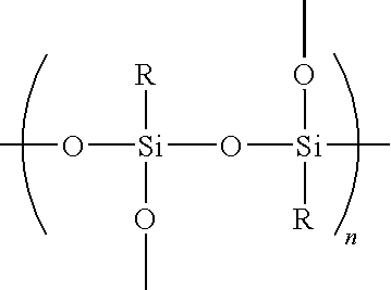
- the organic polysiloxane means a material having a structure wherein a functional group including C, H is included in a bonding-structure of a silicon oxide film, as shown below.
- R means an alkyl group such as a methyl group, an ethyl group, a propyl group or the like; or a derivative thereof; or an aryl group such as a phenyl group: or a derivative thereof.
- the BARC layer 44 and the inorganic-material film 43 are etched while the resist film 45 is used as a mask.
- the state is shown in FIG. 9B .
- the thickness of the resist film 45 is reduced by the etching.
- the organic-material film 42 is etched while the resist film 45 and the inorganic-material film 43 are used as a mask.
- the gate valve 24 of the unit of FIG. 1 is opened, a wafer W of the structure shown in FIG. 9B is conveyed into the chamber 1 by means of a conveying arm, and placed on the supporting table 2 .
- the conveying arm is evacuated, the gate valve 24 is closed, and the supporting table 2 is moved up to a position shown in FIG. 1 .
- the vacuum pump of the gas-discharging system 20 creates a predetermined vacuum in the chamber 1 through the discharging port 19 .
- a predetermined process gas for example an N 2 gas and an O 2 gas
- a pressure in the chamber 1 is maintained at a predetermined pressure, for example about 1.33 to 133.3 Pa (10 to 1000 mTorr).
- a relatively high pressure of 13.3 to 106.7 Pa is preferable.
- a relatively low pressure of 1.33 to 6.67 Pa (10 to 50 mTorr) is preferable. While the pressure in the chamber 1 is maintained within such a predetermined pressure range, a high-frequency electric power whose frequency is 50 to 150 MHz, preferably 70 to 100 MHz, is supplied from the high-frequency electric power source 10 to the supporting table 2 .
- power per unit area hereinafter, referred to as power density
- power density is preferably within a range of about 1.0 to about 5.0 W/cm 2 .
- a range of 2.12 to 4.25 W/cm 2 is preferable. Then, a predetermined electric voltage is applied from the direct current power source 13 to the electrode 6 a of the electrostatic chuck 6 , so that the wafer W sticks to the electrostatic chuck 6 by means of Coulomb force, for example.
- the process gas supplied into the processing space is made plasma, which etches the organic-material film 42 .
- the resist film 45 functions as a mask partway.
- the resist film 45 and the BARC film 44 are etched to disappear. After that, only the inorganic-material film 43 functions as a mask, and the etching process of the organic-material film 42 is continued.
- a magnetic field as shown in FIG. 2 can be formed around the processing space.
- plasma confining effect is achieved, so that an etching rate of the wafer W may be made uniform, even in a case of a high frequency like this embodiment wherein the plasma tends to be not uniform.
- the magnetic field may not have an effect.
- the segment magnets may be caused to revolve in order to conduct the etching process under a condition wherein a magnetic field is substantially not formed around the processing space.
- the effect of making the plasma process uniform can be more enhanced. That is, if the focus ring 5 consists of an electrically conductive material such as silicon or SiC, even a focus-ring region functions as the lower electrode. Thus, a plasma-forming region is expanded over the focus ring 5 , the plasma process around the wafer W is promoted, so that uniformity of the etching rate is improved. In addition, if the focus ring 5 consists of an electrically insulating material such as quartz, electric charges can not be transferred between the focus ring 5 and electrons and ions in the plasma. Thus, the plasma confining effect may be increased so that uniformity of the etching rate is improved.
- the high-frequency electric power for generating plasma and a second high-frequency electric power for drawing ions may be overlapped with each other.
- a second high-frequency electric power source 26 for drawing ions is connected to the matching box 11 , so that they are overlapped.
- the frequency of the second high-frequency electric power source 26 for drawing ions is preferably 3.2 to 13.56 MHz, in particular 13.56 MHz.
- the number of parameters for controlling ion energy is increased so that an optimum processing condition can be easily set wherein an etching rate of the organic-material film is raised more while a necessary and sufficient etching selective ratio with respect to the inorganic-material film is assured.
- the plasma density is dominant, and the ion energy contributes only a little.
- both the plasma density and the ion energy are necessary.
- the plasma density has to be high and the ion energy has to be low.
- the ion energy necessary for etching the inorganic-material film is low and the plasma density dominant for etching the organic-material film is high, only the organic-material film can be selectively etched with a high etching rate.
- the ion energy of the plasma indirectly corresponds to a self-bias electric voltage of an electrode at the etching process.
- FIG. 11 is a graph showing relationships between a self-bias electric voltage Vdc and plasma density Ne, in respective cases wherein the frequency of the high-frequency electric power is 40 MHz or 100 MHz.
- the transverse axis represents the self-bias electric voltage Vdc
- the ordinate axis represents the plasma density.
- Ar was used for evaluation, instead of real etching gas.
- applied high-frequency electric power was changed, so that values of the plasma density Ne and the self-bias electric voltage Vdc were changed. That is, in the respective frequencies, if the applied high-frequency electric power is large, both the plasma density Ne and the self-bias electric voltage Vdc are large.
- the plasma density was measured by means of a microwave interferometer.
- the self-bias electric voltage Vdc is greatly increased.
- the frequency of the high-frequency electric power is 100 MHz that is higher than prior art, even when the plasma density is increased, the self-bias electric voltage Vdc is not so increased and controlled substantially not higher than 100 V. That is, it was found that a condition of high plasma density and low self-bias electric voltage can be achieved.
- the frequency is relatively low like a conventional art, when the etching rate of the organic-material film is increased in a real etching process, the inorganic-material film is also etched to the same extent and good selective-etching performance is not achieved.
- the frequency is as high as 100 MHz, it was found that the organic-material film can be etched with a high etching rate and a high etching selective ratio with respect to the inorganic-material film.
- the plasma of Ar gas when the plasma of Ar gas is formed, it may be thought preferable to form the plasma under a condition wherein the plasma density is not less than 1 ⁇ 10 11 cm ⁇ 3 and the self-bias electric voltage of the electrode is not higher than 300 V. More preferably, the plasma density is not less than 1.5 ⁇ 10 11 cm ⁇ 3 and the self-bias electric voltage of the electrode is not higher than 100 V. Then, in order to satisfy such a plasma condition, it may be estimated that the frequency of the high-frequency electric power has to be 50 MHz or higher.
- the frequency of the high-frequency electric power for generating plasma is set not less than 50 MHz, as described above. However, if the frequency of the high-frequency electric power for generating plasma is higher than 150 MHz, the uniformity of the plasma may be deteriorated. Thus, it is preferable that the frequency of the high-frequency electric power for generating plasma is not higher than 150 MHz. In particular, in order to effectively achieve the above effect, it is preferable that the frequency of the high-frequency electric power for generating plasma is 70 to 100 MHz.
- FIG. 12 is a graph comparatively showing relationships between a self-bias electric voltage and plasma density, in respective cases wherein the plasma is formed by an Ar gas or an etching gas, when the frequency of the high-frequency electric power is 100 MHz.
- the transverse axis represents the self-bias electric voltage Vdc, and the ordinate axis represents the plasma density.
- the pressure in the chamber was 13.3 Pa (100 mTorr).
- the power of the high-frequency electric power of 100 MHz was changed, so that the plasma density and the self-bias electric voltage Vdc were changed.
- the power of the high-frequency electric power of 100 MHz was fixed to 2500 W while a second high-frequency electric power of 3.2 MHz was overlapped in a range of 200 to 3000 W.
- the plasma density tends to be a little lower.
- the second high-frequency electric power of the lower frequency (3.2 MHz) is overlapped and the power is increased, the self-bias electric voltage tends to be increased.
- the plasma density tends to be higher and the self-bias electric voltage tends to be lower than the conventional art.
- the etching process can be conducted with a high etching rate while satisfying an etching selective ratio with respect to the inorganic-material film.
- the plasma density becomes 1 ⁇ 10 11 cm ⁇ 3 and the self-bias electric voltage becomes about 200 V.
- the plasma density becomes about 1 ⁇ 10 11 to 2 ⁇ 10 11 cm ⁇ 3 and the self-bias electric voltage becomes about 800 to 900 V.
- the overlapped power of 3.2 MHz is increased, it is thought that the etching rate is also increased.
- the self-bias electric voltage is increased, the etching selective ratio with respect to the inorganic-material film tends to be lowered.
- the etching selective ratio can be maintained in an allowable range.
- the overlapped power (bias power) of the second high-frequency electric power is increased, the etching rate may be enhanced while an etching selective ratio of a desirable level is maintained. That is, under a condition wherein the plasma density is 5 ⁇ 10 10 to 2 ⁇ 10 11 cm ⁇ 3 and the self-bias electric voltage of the electrode is not higher than 900 V, it is possible that the etching process is conducted with a high etching rate while maintaining the etching selective ratio with respect to the inorganic-material film within a desirable range.
- a pressure in the chamber 1 is 13.3 to 106.7 pa (100 to 800 mTorr) that is high; a first high-frequency electric power having a frequency of 50 to 150 MHz, for example 100 MHz, and a power density of 2.12 to 4.25 W/cm 2 is applied to the supporting table 2 ; if necessary, a second high-frequency electric power having a frequency of 500 kHz to 27 MHz, for example 3.2 MHz, and a power density of not higher than 4.25 W/cm 2 is applied to be overlapped with the first high-frequency electric power; the plasma density is 5 ⁇ 10 10 to 2 ⁇ 10 11 cm ⁇ 3 ; and the self-bias electric voltage Vdc of the supporting table 2 as the lower electrode is not higher than 900 V.
- the bias power is adjusted so that the organic-material film can be etched with a high etching selective ratio with respect to the inorganic-material film and with a high etching rate.
- a very high etching rate can be achieved while a high etching selective ratio can be maintained.
- a pressure in the chamber 1 is 1.33 to 6.67 pa (10 to 50 mTorr) that is low; a first high-frequency electric power having a frequency of 50 to 150 MHz, for example 100 MHz, and a power density of 2.12 to 4.25 W/cm 2 is applied to the supporting table 2 ; if necessary, a second high-frequency electric power having a frequency of 500 kHz to 27 MHz, for example 3.2 MHz, and a power density of not higher than 0.566 W/cm 2 is applied to be overlapped with the first high-frequency electric power; the plasma density is 5 ⁇ 10 10 to 2 ⁇ 10 11 cm ⁇ 3 ; and the self-bias electric voltage Vdc of the supporting table 2 as the lower electrode is not higher than 400 V.
- the pressure in the chamber 1 is low, ion energy itself can be controlled not higher than energy by which the inorganic-material film can be spattered.
- the self-bias electric voltage is limited within the relatively low range.
- the organic-material film can be etched with a high etching rate and a very high etching selective ratio with respect to the inorganic-material film.
- surface residue is substantially not left.
- a CD-shift of the mask of the inorganic-material film can be remarkably reduced.
- FIG. 13A is a graph showing etching rates of an organic-material film at a wafer position, in respective cases wherein the high-frequency electric power is 500 W (1.59 W/cm 2 ), 1000 W (3.18 W/cm 2 ) or 1500 W (4.77 W/cm 2 ), when the frequency of the high-frequency electric power is 100 MHz.
- FIG. 13B is a graph showing etching rates of an organic-material film at a wafer position, in respective cases wherein the high-frequency electric power is 500 W (1.59 W/cm 2 ), 1000 W (3.18 W/cm 2 ) or 1500 W (4.77 W/cm 2 ), when the frequency of the high-frequency electric power is 40 MHz.
- FIG. 13A is a graph showing etching rates of an organic-material film at a wafer position, in respective cases wherein the high-frequency electric power is 500 W (1.59 W/cm 2 ), 1000 W (3.18 W/cm 2 ) or 1500 W (4.77 W/
- FIG. 14 is a graph showing relationships between a high-frequency electric power and an etching rate of the organic-material film, in respective cases wherein the frequency of the high-frequency electric power is 40 MHz or 100 MHz.
- FIG. 15 is a graph showing relationships between a high-frequency electric power and an etching rate of the inorganic-material film, in respective cases wherein the frequency of the high-frequency electric power is 40 MHz or 100 MHz.
- FIG. 16 is a graph showing relationships between an etching rate of the organic-material film and a ratio (an etching rate of the organic-material film/an etching rate of the inorganic-material film) corresponding to an etching selective ratio, in respective cases wherein the frequency of the high-frequency electric power is 40 MHz or 100 MHz.
- the etching rate of the organic-material film is higher in the case of 100 MHz, for every power.
- the etching rate of the inorganic-material film tends to be increased.
- the difference between the etching rate in the case of 40 MHz and the etching rate in the case of 100 MHz is not large.
- the etching rate of the organic-material film is higher, and when the high-frequency electric power is lower, the value corresponding to the etching selective ratio with respect to the inorganic-material film tends to be higher.
- the etching rate in the case of 40 MHz when the value corresponding to the etching selective ratio is the same, the etching rate in the case of 100 MHz is higher. Comparing them at the same etching rate, the value corresponding to the etching selective ratio in the case of 100 MHz is larger than the value corresponding to the etching selective ratio in the case of 40 MHz. That is, from the experimental result of the samples for estimation, it was confirmed that the possibility of etching the organic-material film with a high etching rate and a high etching selective ratio is higher in the case of 100 MHz than in the case of 40 MHz.
- the power of the high-frequency electric power of 100 MHz is preferably in a range of about 1.0 W/cm 2 to about 5.0 W/cm 2 , because the etching rate and the etching selective ratio of the organic-material film are in a tradeoff relationship.
- the organic-material film 42 consisting of a low-k film was etched by the unit shown in FIG. 1 by using the high-frequency electric power of 40 MHz and 100 MHz, respectively.
- the etching condition of this case was the same as that in the above etching experiment of the whole-surface formed films.
- SiLK commercial name
- DowChemical company was used as the organic-material film 42 .
- a thickness thereof was 570 nm
- a thickness of the SiO 2 film 43 thereon was 200 nm
- a thickness of the BARC film 44 thereon was 60 nm
- a thickness of the resist film 45 was 800 nm.
- the etching process was continued for a time that is 1.5 times as long as that until the organic-material film 42 is completely etched (50% over etching).
- the time for which the SiO 2 film is exposed to the plasma was lengthened. That is, the condition was severe on the SiO 2 film.
- FIG. 17 is a graph showing relationships between a high-frequency electric power and an etching rate of the organic-material film and relationships between a high-frequency electric power and a shoulder loss of the inorganic-material film.
- FIG. 18 is a graph showing relationships between an etching rate of the organic-material film and an etching selective ratio with respect to an etching rate of a shoulder part of the inorganic-material film, in respective cases wherein the frequency of the high-frequency electric power is 40 MHz or 100 MHz.
- the shoulder loss means an etched volume of the shoulder part. Specifically, as shown in FIG.
- the shoulder loss means a height distance (shown by Y in the drawing) from the original surface of the inorganic-material film 43 to an etched (deepest) position of the shoulder part.
- the etching selective ratio at the shoulder part in FIG. 18 means a ratio of the etching rate of the organic-material film with respect to the etching rate at the shoulder part of the inorganic-material film 43 calculated from the value of the shoulder loss.
- the shoulder loss is at the same level, but the etching rate of the organic-material film is higher in the case of 100 MHz.
- FIG. 18 in the real pattern, in the same manner as FIG. 16 showing the results of the samples for estimation, when the etching selective ratio is the same, the etching rate of the organic-material film is higher in the case of 100 MHz. When the etching rate is the same, the etching selective ratio tends to be higher in the case of 100 MHz.
- the organic-material film can be etched with a high etching rate and a high etching selective ratio when the high-frequency electric power of 100 MHz, other than 40 MHz, is used.
- the gap between the electrodes was 27 mm.
- the distance between the electrodes is preferably 35 to 50 mm. This is explained with reference to FIG. 20 .
- FIG. 20 is a graph comparatively showing relationships between an Ar-gas flow rate and a pressure difference ⁇ P of a central portion of the wafer and a peripheral portion thereof, in respective cases wherein the electrode gap is 25 mm or 40 mm, wherein the Ar gas is used as a plasma gas.
- the pressure difference ⁇ P is smaller when the gap is 40 mm rather than 25 mm.
- the pressure difference ⁇ P tends to be sharply increased.
- the gas flow rate When the gas flow rate is higher than about 0.3 L/min, it exceeds 0.27 Pa (2 mTorr) as an allowable maximum pressure difference ⁇ P, at which deterioration of the etching uniformity or the like may not be generated.
- the pressure difference is smaller than 0.27 Pa (2 mTorr).
- the process gas an N 2 gas and an H 2 gas were used.
- the pressure in the chamber was changed between 13.3 Pa (100 mTorr), 31.7 Pa (450 mTorr) and 106.7 Pa (800 mTorr).
- the flow rate of the process gas was the N 2 gas: 0.5 L/min and the H 2 gas: 0.5 L/min in the case of 13.3 Pa, and the N 2 gas: 0.65 L/min and the H 2 gas: 0.65 L/min in the cases of 31.7 Pa and 106.7 Pa.
- the electrode gap was 40 mm.
- the etching process was conducted as 50% over etching in the same manner as the above example.
- FIG. 21 is a graph showing relationships between the power of the second high-frequency electric power of 3.2 MHz and an etching rate of the organic-material film and relationships between the power of the second high-frequency electric power of 3.2 MHz and an etching selective ratio with respect to the shoulder part, in respective pressure conditions.
- FIG. 22 is a graph showing relationships between the power of the second high-frequency electric power of 3.2 MHz and a top CD shift, in respective pressure conditions.
- FIG. 23 is a graph showing relationships between the power of the second high-frequency electric power of 3.2 MHz and a bowing value, in respective pressure conditions.
- FIG. 21 is a graph showing relationships between the power of the second high-frequency electric power of 3.2 MHz and an etching rate of the organic-material film and relationships between the power of the second high-frequency electric power of 3.2 MHz and an etching selective ratio with respect to the shoulder part, in respective pressure conditions.
- FIG. 22 is a graph showing relationships between the power of the second high-frequency electric power of 3.2
- the top CD shift means a value showing how much a top CD is changed through the etching process, the top CD meaning an etching opening at an upper-end portion of the organic-material film 42 . That is, the top CD shift means a value obtained by subtracting an original top CD (TopCDbf) from a top CD after the etching process (TopCDaf). In addition, the bowing value means a value obtained by subtracting the top CD (TopCD) from a maximum width (MaxCD) at an etched portion after the etching process of the organic-material film.
- the pressure in the chamber is 13.3 Pa or higher, ion dispersion is great, so that vertical component of ion energy is relatively reduced.
- the power of the second high-frequency electric power (bias power) of 3.2 MHz is relatively low, the inorganic-material mask is hardly etched. That is, the organic-material film can be etched with a high etching selective ratio with respect to the inorganic-material mask. Furthermore, in the case, the etching rate of the organic-material film is also high. In addition, at the same bias power, the etching selective ratio tends to be higher under a condition of a higher pressure wherein the vertical component of ion energy is less.
- the etching selective ratio is deteriorated.
- the bias power is 1600 W (power density: 2.26 W/cm 2 ) that is high
- the etching rate of the organic-material film is 400 nm/min that is high, but the etching selective ratio is reduced to about 3 or 4. This feature is usable for some applications.
- a bias power higher than the above is not usable because the etching loss of the inorganic-material mask is too much.
- the bias power is 3000 W (power density: 4.25 W/cm 2 )
- the etching selective ratio is maintained at about 5. This feature is usable for some applications.
- the etching rate of the organic-material film is 550 nm/min, which is very high.
- a bias power higher than 3000 W power density: 4.25 W/cm 2
- the etching loss of the inorganic-material mask is too much.
- the top CD shift tends to be better in the case of the pressure of 13.3 Pa than in the case of the pressure of 106.7 Pa. Furthermore, in the case of 13.3 Pa, when the bias power is increased, the top CD shift is reduced, and when the bias power is 1600 W (power density: 2.26 W/cm 2 ), the top CD shift is about 2 to 3 nm. In the case of the pressure of 106.7 Pa, independently on the bias power, the top CD shift is 30 nm. In the case of the pressure of 106.7 Pa, the top CD shift is near to the upper limit of an allowable range. Thus, the substantially upper limit of the pressure in the chamber is 106.7 Pa.
- the bowing value tends to be lower in the case of the pressure of 106.7 Pa than in the case of the pressure of 13.3 Pa, at the same bias power.
- the bowing value is increased, and when the bias power is 3000 W (power density: 4.25 W/cm 2 ), the bowing value is 30 nm.
- the bias power is higher than 3000 W, it is expected that the bowing value exceeds 30 nm.
- the upper limit of the bias power is 3000 W (power density: 4.25 W/cm 2 ).
- the pressure in the chamber was changed between 1.33 Pa (10 mTorr), 3.99 Pa (30 mTorr), 6.65 Pa (50 mTorr) and 13.3 Pa (100 mTorr).
- the flow rate of the process gas was the N 2 gas: 0.12 L/min and the H 2 gas: 0.12 L/min in the case of 1.33 Pa, the N 2 gas: 0.18 L/min and the H 2 gas: 0.18 L/min in the cases of 3.99 Pa, the N 2 gas: 0.3 L/min and the H 2 gas: 0.3 L/min in the cases of 6.65 Pa and the N 2 gas: 0.5 L/min and the H 2 gas: 0.5 L/min in the cases of 13.3 Pa.
- the electrode gap was 40 mm.
- the etching process was conducted as 50% over etching in the same manner as the above examples.
- FIGS. 26 and 27 For each sample after the etching process, an etching residue, a shoulder loss of the inorganic-material film (mask) and a top CD shift were obtained. The result is shown in FIGS. 26 and 27 .
- FIG. 26 is a graph showing etching residues, shoulder losses of the inorganic-material film (mask) and top CD shifts, in respective pressure conditions, when the bias power (of the second high-frequency electric power source) is zero.
- FIG. 27 is a graph showing shoulder losses of the inorganic-material film (mask), top CD shifts and etching rates of the organic-material film, in respective bias-power conditions, when the pressure is 3.99 Pa.
- the shoulder loss of the inorganic-material film was 0 in the cases of 3.99 Pa, 6.65 Pa and 13.3 Pa.
- the shoulder loss of the inorganic-material film was 42 nm in the case of 1.33 Pa, which value is relatively large but within an allowable range.
- the top CD shift was ⁇ 3 nm in the case of 3.99 Pa, and +5 nm in the case of 6.65 Pa, which values are very small. In addition, it was confirmed that the absolute value of the top CD shift is increased both when the pressure is higher than 6.65 Pa and when the pressure is lower than 3.99 Pa.
- the top CD shift was ⁇ 30 nm in the case of 1.33 Pa, which value is approximately within an allowable range. From these results, it was confirmed that the pressure is preferably within a range of 1.33 to 6.65 Pa in order to conduct an etching process wherein the shoulder loss is small (that is, the etching selective ratio is high), the etching residue is less, and the top CD shift is small.
- the shoulder loss tends to be increased and the absolute value of the top CD shift tends to be increased.
- the bias power is 400 W (power density: 0.566 W/cm 2 ) or lower, the respective values of the shoulder loss and the top CD shift were within usable ranges. It is estimated that the shoulder loss becomes too large when the bias power exceeds 400 W.
- the etching rate tends to be increased when the bias power is increased.
- the present invention is not limited to the above embodiment, but may be variously modified.
- the magnetic-field generating means the annular magnetic unit in the multi-pole state is used wherein the plurality of segment magnets consisting of permanent magnets are arranged annularly around the chamber.
- the present invention is not limited to this manner if a magnetic-field can be formed around the processing space to confine the plasma.
- the peripheral magnetic field for confining the plasma may be unnecessary. That is, the etching process can be conducted under a condition wherein there is no magnetic field.
- the present invention can be applied to a plasma etching process conducted in a crossed electromagnetic field wherein a horizontal magnetic field is applied to the processing space.
- the high-frequency electric power for generating plasma is applied to the lower electrode, but may be applied to the upper electrode.
- the low-k film is used as the organic-material film, but other films including O, C and H or other films including Si, O, C and H may be also used.
- the semiconductor wafer is taken as an example of the substrate to be processed.
- this invention is not limited thereto, but applicable to other plasma processes for an LCD substrate or the like.
- the above description is about the case wherein the organic-material film is etched by using the inorganic-material film as a mask, but this invention is not limited thereto. This invention is applicable to all cases to selectively etch an organic-material film with respect to an inorganic-material film.
- this invention is applicable to an ashing process to remove a resist that has been used as a mask when an inorganic-material film, for example a SiO 2 film, formed on a substrate to be processed, for example a Si wafer or the like, is etched.
- the ashing process has to be conducted so as to selectively and efficiently remove the resist film being an organic-material film, with etching the inorganic-material film under the resist film as little as possible.
- the present invention is applied to the ashing process, a good ashing characteristic can be achieved.
Abstract
Description
Claims (20)
Priority Applications (1)
| Application Number | Priority Date | Filing Date | Title |
|---|---|---|---|
| US12/578,007 US8840753B2 (en) | 2001-12-05 | 2009-10-13 | Plasma etching unit |
Applications Claiming Priority (8)
| Application Number | Priority Date | Filing Date | Title |
|---|---|---|---|
| JP2007-370898 | 2001-12-05 | ||
| JP2001-370898 | 2001-12-05 | ||
| JP2001370898 | 2001-12-05 | ||
| JP2002-127051 | 2002-04-26 | ||
| JP2002127051A JP2003234331A (en) | 2001-12-05 | 2002-04-26 | Plasma etching method and apparatus |
| PCT/JP2002/012720 WO2003049169A1 (en) | 2001-12-05 | 2002-12-04 | Plasma etching method and plasma etching device |
| US10/860,152 US7625494B2 (en) | 2001-12-05 | 2004-06-04 | Plasma etching method and plasma etching unit |
| US12/578,007 US8840753B2 (en) | 2001-12-05 | 2009-10-13 | Plasma etching unit |
Related Parent Applications (1)
| Application Number | Title | Priority Date | Filing Date |
|---|---|---|---|
| US10/860,152 Division US7625494B2 (en) | 2001-12-05 | 2004-06-04 | Plasma etching method and plasma etching unit |
Publications (2)
| Publication Number | Publication Date |
|---|---|
| US20100024983A1 US20100024983A1 (en) | 2010-02-04 |
| US8840753B2 true US8840753B2 (en) | 2014-09-23 |
Family
ID=26624882
Family Applications (2)
| Application Number | Title | Priority Date | Filing Date |
|---|---|---|---|
| US10/860,152 Expired - Fee Related US7625494B2 (en) | 2001-12-05 | 2004-06-04 | Plasma etching method and plasma etching unit |
| US12/578,007 Expired - Fee Related US8840753B2 (en) | 2001-12-05 | 2009-10-13 | Plasma etching unit |
Family Applications Before (1)
| Application Number | Title | Priority Date | Filing Date |
|---|---|---|---|
| US10/860,152 Expired - Fee Related US7625494B2 (en) | 2001-12-05 | 2004-06-04 | Plasma etching method and plasma etching unit |
Country Status (5)
| Country | Link |
|---|---|
| US (2) | US7625494B2 (en) |
| JP (1) | JP2003234331A (en) |
| AU (1) | AU2002349419A1 (en) |
| TW (1) | TWI263276B (en) |
| WO (1) | WO2003049169A1 (en) |
Families Citing this family (43)
| Publication number | Priority date | Publication date | Assignee | Title |
|---|---|---|---|---|
| JP2003234331A (en) | 2001-12-05 | 2003-08-22 | Tokyo Electron Ltd | Plasma etching method and apparatus |
| US7517801B1 (en) * | 2003-12-23 | 2009-04-14 | Lam Research Corporation | Method for selectivity control in a plasma processing system |
| US8222155B2 (en) | 2004-06-29 | 2012-07-17 | Lam Research Corporation | Selectivity control in a plasma processing system |
| JP4827081B2 (en) * | 2005-12-28 | 2011-11-30 | 東京エレクトロン株式会社 | Plasma etching method and computer-readable storage medium |
| US7914692B2 (en) * | 2006-08-29 | 2011-03-29 | Ngk Insulators, Ltd. | Methods of generating plasma, of etching an organic material film, of generating minus ions, of oxidation and nitriding |
| US7851367B2 (en) | 2006-08-31 | 2010-12-14 | Kabushiki Kaisha Toshiba | Method for plasma processing a substrate |
| JP2008060429A (en) * | 2006-08-31 | 2008-03-13 | Toshiba Corp | Plasma treatment apparatus and plasma treatment method of substrate |
| US7977244B2 (en) | 2006-12-18 | 2011-07-12 | United Microelectronics Corp. | Semiconductor manufacturing process |
| US7938976B2 (en) * | 2007-02-27 | 2011-05-10 | International Business Machines Corporation | Method of removing graphitic and/or fluorinated organic layers from the surface of a chip passivation layer having Si-containing compounds |
| JP4660498B2 (en) | 2007-03-27 | 2011-03-30 | 株式会社東芝 | Substrate plasma processing equipment |
| JP4607930B2 (en) * | 2007-09-14 | 2011-01-05 | 株式会社東芝 | Plasma processing apparatus and plasma processing method |
| JP5224837B2 (en) | 2008-02-01 | 2013-07-03 | 株式会社東芝 | Substrate plasma processing apparatus and plasma processing method |
| JP4756063B2 (en) * | 2008-08-15 | 2011-08-24 | 株式会社東芝 | Manufacturing method of semiconductor device |
| JP5295833B2 (en) | 2008-09-24 | 2013-09-18 | 株式会社東芝 | Substrate processing apparatus and substrate processing method |
| JP5395491B2 (en) | 2009-03-31 | 2014-01-22 | 東京エレクトロン株式会社 | Substrate processing apparatus and substrate processing method |
| EP3222749A1 (en) | 2009-05-13 | 2017-09-27 | SiO2 Medical Products, Inc. | Outgassing method for inspecting a coated surface |
| WO2013170052A1 (en) | 2012-05-09 | 2013-11-14 | Sio2 Medical Products, Inc. | Saccharide protective coating for pharmaceutical package |
| US9458536B2 (en) | 2009-07-02 | 2016-10-04 | Sio2 Medical Products, Inc. | PECVD coating methods for capped syringes, cartridges and other articles |
| JP2011192776A (en) * | 2010-03-15 | 2011-09-29 | Toshiba Corp | Method of manufacturing semiconductor device |
| WO2011115008A1 (en) * | 2010-03-16 | 2011-09-22 | 株式会社 アルバック | Etching method and etching device |
| US11624115B2 (en) | 2010-05-12 | 2023-04-11 | Sio2 Medical Products, Inc. | Syringe with PECVD lubrication |
| US9878101B2 (en) | 2010-11-12 | 2018-01-30 | Sio2 Medical Products, Inc. | Cyclic olefin polymer vessels and vessel coating methods |
| JP5709505B2 (en) * | 2010-12-15 | 2015-04-30 | 東京エレクトロン株式会社 | Plasma processing apparatus, plasma processing method, and storage medium |
| US9272095B2 (en) | 2011-04-01 | 2016-03-01 | Sio2 Medical Products, Inc. | Vessels, contact surfaces, and coating and inspection apparatus and methods |
| US11116695B2 (en) | 2011-11-11 | 2021-09-14 | Sio2 Medical Products, Inc. | Blood sample collection tube |
| EP2776603B1 (en) | 2011-11-11 | 2019-03-06 | SiO2 Medical Products, Inc. | PASSIVATION, pH PROTECTIVE OR LUBRICITY COATING FOR PHARMACEUTICAL PACKAGE, COATING PROCESS AND APPARATUS |
| US9554968B2 (en) | 2013-03-11 | 2017-01-31 | Sio2 Medical Products, Inc. | Trilayer coated pharmaceutical packaging |
| JP6207880B2 (en) * | 2012-09-26 | 2017-10-04 | 東芝メモリ株式会社 | Plasma processing apparatus and plasma processing method |
| CA2890066C (en) | 2012-11-01 | 2021-11-09 | Sio2 Medical Products, Inc. | Coating inspection method |
| EP2920567B1 (en) | 2012-11-16 | 2020-08-19 | SiO2 Medical Products, Inc. | Method and apparatus for detecting rapid barrier coating integrity characteristics |
| US9764093B2 (en) | 2012-11-30 | 2017-09-19 | Sio2 Medical Products, Inc. | Controlling the uniformity of PECVD deposition |
| CN105705676B (en) | 2012-11-30 | 2018-09-07 | Sio2医药产品公司 | Control the uniformity of the PECVD depositions on injector for medical purpose, cylindrantherae etc. |
| CN103903945B (en) * | 2012-12-24 | 2016-04-20 | 中微半导体设备(上海)有限公司 | A kind of method of stable pulse radio frequency |
| US20160015898A1 (en) | 2013-03-01 | 2016-01-21 | Sio2 Medical Products, Inc. | Plasma or cvd pre-treatment for lubricated pharmaceutical package, coating process and apparatus |
| US9937099B2 (en) | 2013-03-11 | 2018-04-10 | Sio2 Medical Products, Inc. | Trilayer coated pharmaceutical packaging with low oxygen transmission rate |
| US9863042B2 (en) | 2013-03-15 | 2018-01-09 | Sio2 Medical Products, Inc. | PECVD lubricity vessel coating, coating process and apparatus providing different power levels in two phases |
| EP3122917B1 (en) | 2014-03-28 | 2020-05-06 | SiO2 Medical Products, Inc. | Antistatic coatings for plastic vessels |
| JP2016092102A (en) * | 2014-10-31 | 2016-05-23 | 東京エレクトロン株式会社 | Method for etching organic film |
| WO2017031354A2 (en) | 2015-08-18 | 2017-02-23 | Sio2 Medical Products, Inc. | Pharmaceutical and other packaging with low oxygen transmission rate |
| KR102140001B1 (en) * | 2016-12-02 | 2020-07-31 | 가부시키가이샤 아루박 | Wiring board processing method |
| CN112889128B (en) | 2018-11-05 | 2024-04-12 | 应用材料公司 | Magnetic housing system |
| WO2021034698A1 (en) * | 2019-08-16 | 2021-02-25 | Applied Materials, Inc. | Tuneable uniformity control utilizing rotational magnetic housing |
| CN117423716B (en) * | 2023-12-19 | 2024-04-09 | 合肥晶合集成电路股份有限公司 | Back-illuminated semiconductor structure etching method and etching device |
Citations (37)
| Publication number | Priority date | Publication date | Assignee | Title |
|---|---|---|---|---|
| US4401054A (en) * | 1980-05-02 | 1983-08-30 | Nippon Telegraph & Telephone Public Corporation | Plasma deposition apparatus |
| US4492610A (en) | 1980-12-11 | 1985-01-08 | Tokyo Shibaura Denki Kabushiki Kaisha | Dry Etching method and device therefor |
| US4894510A (en) | 1986-09-05 | 1990-01-16 | Mitsubishi Denki Kabushiki Kaisha | Apparatus for uniformly distributing plasma over a substrate |
| JPH06181187A (en) | 1992-12-11 | 1994-06-28 | Hitachi Ltd | Sputtering system |
| US5444207A (en) * | 1992-03-26 | 1995-08-22 | Kabushiki Kaisha Toshiba | Plasma generating device and surface processing device and method for processing wafers in a uniform magnetic field |
| US5543184A (en) * | 1993-12-23 | 1996-08-06 | International Business Machines Corporation | Method of reducing particulates in a plasma tool through steady state flows |
| US5556474A (en) * | 1993-12-14 | 1996-09-17 | Nissin Electric Co., Ltd. | Plasma processing apparatus |
| JPH098009A (en) | 1995-06-16 | 1997-01-10 | Tokyo Electron Ltd | Plasma processor |
| US5659276A (en) * | 1995-07-12 | 1997-08-19 | Shin-Etsu Chemical Co., Ltd. | Magnetic field generator for magnetron plasma |
| US5837615A (en) | 1995-09-21 | 1998-11-17 | Lsi Logic Corporation | Integrated circuit device fabrication by plasma etching |
| US6014943A (en) * | 1996-09-12 | 2000-01-18 | Tokyo Electron Limited | Plasma process device |
| JP2000173995A (en) | 1998-12-03 | 2000-06-23 | Matsushita Electric Ind Co Ltd | Apparatus and method for plasma etching |
| US6089181A (en) * | 1996-07-23 | 2000-07-18 | Tokyo Electron Limited | Plasma processing apparatus |
| JP2000269196A (en) | 1999-03-19 | 2000-09-29 | Toshiba Corp | Method and apparatus for plasma treatment |
| US6129044A (en) * | 1996-07-12 | 2000-10-10 | Applied Materials, Inc. | Apparatus for substrate processing with improved throughput and yield |
| WO2000079586A1 (en) | 1999-06-24 | 2000-12-28 | Hitachi, Ltd. | Production method for semiconductor integrated circuit device and semiconductor integrated circuit device |
| US6171438B1 (en) | 1995-03-16 | 2001-01-09 | Hitachi, Ltd. | Plasma processing apparatus and plasma processing method |
| US6190496B1 (en) * | 1996-07-03 | 2001-02-20 | Tegal Corporation | Plasma etch reactor and method for emerging films |
| US6197151B1 (en) | 1996-03-01 | 2001-03-06 | Hitachi, Ltd. | Plasma processing apparatus and plasma processing method |
| JP2001118830A (en) | 1999-10-19 | 2001-04-27 | Tokyo Electron Ltd | Plasma treatment method |
| JP2001118825A (en) | 1999-10-19 | 2001-04-27 | Tokyo Electron Ltd | Etching method |
| US20010034137A1 (en) | 2000-04-21 | 2001-10-25 | Hidetaka Nambu | Semiconductor device and manufacturing method of the device |
| JP2001338912A (en) * | 2000-05-29 | 2001-12-07 | Tokyo Electron Ltd | Plasma processing equipment and method for processing thereof |
| US20020011462A1 (en) | 2000-07-27 | 2002-01-31 | Harald Richter | Method of processing organic antireflection layers |
| US20020061654A1 (en) | 2000-04-19 | 2002-05-23 | Kenshi Kanegae | Etching method, semiconductor and fabricating method for the same |
| US6423242B1 (en) | 1998-12-02 | 2002-07-23 | Tokyo Electron Limited | Etching method |
| US6426477B1 (en) | 1999-09-13 | 2002-07-30 | Tokyo Electron Limited | Plasma processing method and apparatus for eliminating damages in a plasma process of a substrate |
| US6514377B1 (en) | 1999-09-08 | 2003-02-04 | Tokyo Electron Limited | Apparatus for and method of processing an object to be processed |
| US6518191B2 (en) | 2000-05-26 | 2003-02-11 | Matsushita Electric Industrial Co., Ltd. | Method for etching organic film, method for fabricating semiconductor device and pattern formation method |
| WO2003049169A1 (en) | 2001-12-05 | 2003-06-12 | Tokyo Electron Limited | Plasma etching method and plasma etching device |
| US6635185B2 (en) | 1997-12-31 | 2003-10-21 | Alliedsignal Inc. | Method of etching and cleaning using fluorinated carbonyl compounds |
| US6642149B2 (en) | 1998-09-16 | 2003-11-04 | Tokyo Electron Limited | Plasma processing method |
| US20040076762A1 (en) | 2001-03-06 | 2004-04-22 | Etsuo Iijima | Plasma processor and plasma processing method |
| US20040085706A1 (en) | 2002-06-06 | 2004-05-06 | Riki Tomoyoshi | Electrostatic chuck, supporting table and plasma processing system |
| US7419613B2 (en) | 2002-12-27 | 2008-09-02 | Tokyo Electron Limited | Method and device for plasma-etching organic material film |
| US7438783B2 (en) | 2004-10-15 | 2008-10-21 | Shin-Etsu Chemical Co., Ltd. | Plasma processing apparatus and plasma processing method |
| US7473377B2 (en) | 2002-06-27 | 2009-01-06 | Tokyo Electron Limited | Plasma processing method |
-
2002
- 2002-04-26 JP JP2002127051A patent/JP2003234331A/en active Pending
- 2002-12-04 WO PCT/JP2002/012720 patent/WO2003049169A1/en active Application Filing
- 2002-12-04 AU AU2002349419A patent/AU2002349419A1/en not_active Abandoned
- 2002-12-04 TW TW91135187A patent/TWI263276B/en not_active IP Right Cessation
-
2004
- 2004-06-04 US US10/860,152 patent/US7625494B2/en not_active Expired - Fee Related
-
2009
- 2009-10-13 US US12/578,007 patent/US8840753B2/en not_active Expired - Fee Related
Patent Citations (38)
| Publication number | Priority date | Publication date | Assignee | Title |
|---|---|---|---|---|
| US4401054A (en) * | 1980-05-02 | 1983-08-30 | Nippon Telegraph & Telephone Public Corporation | Plasma deposition apparatus |
| US4492610A (en) | 1980-12-11 | 1985-01-08 | Tokyo Shibaura Denki Kabushiki Kaisha | Dry Etching method and device therefor |
| US4894510A (en) | 1986-09-05 | 1990-01-16 | Mitsubishi Denki Kabushiki Kaisha | Apparatus for uniformly distributing plasma over a substrate |
| US5444207A (en) * | 1992-03-26 | 1995-08-22 | Kabushiki Kaisha Toshiba | Plasma generating device and surface processing device and method for processing wafers in a uniform magnetic field |
| JPH06181187A (en) | 1992-12-11 | 1994-06-28 | Hitachi Ltd | Sputtering system |
| US5556474A (en) * | 1993-12-14 | 1996-09-17 | Nissin Electric Co., Ltd. | Plasma processing apparatus |
| US5543184A (en) * | 1993-12-23 | 1996-08-06 | International Business Machines Corporation | Method of reducing particulates in a plasma tool through steady state flows |
| US6171438B1 (en) | 1995-03-16 | 2001-01-09 | Hitachi, Ltd. | Plasma processing apparatus and plasma processing method |
| JPH098009A (en) | 1995-06-16 | 1997-01-10 | Tokyo Electron Ltd | Plasma processor |
| US5659276A (en) * | 1995-07-12 | 1997-08-19 | Shin-Etsu Chemical Co., Ltd. | Magnetic field generator for magnetron plasma |
| US5837615A (en) | 1995-09-21 | 1998-11-17 | Lsi Logic Corporation | Integrated circuit device fabrication by plasma etching |
| US6197151B1 (en) | 1996-03-01 | 2001-03-06 | Hitachi, Ltd. | Plasma processing apparatus and plasma processing method |
| US6190496B1 (en) * | 1996-07-03 | 2001-02-20 | Tegal Corporation | Plasma etch reactor and method for emerging films |
| US6129044A (en) * | 1996-07-12 | 2000-10-10 | Applied Materials, Inc. | Apparatus for substrate processing with improved throughput and yield |
| US6089181A (en) * | 1996-07-23 | 2000-07-18 | Tokyo Electron Limited | Plasma processing apparatus |
| US6014943A (en) * | 1996-09-12 | 2000-01-18 | Tokyo Electron Limited | Plasma process device |
| US6635185B2 (en) | 1997-12-31 | 2003-10-21 | Alliedsignal Inc. | Method of etching and cleaning using fluorinated carbonyl compounds |
| US6642149B2 (en) | 1998-09-16 | 2003-11-04 | Tokyo Electron Limited | Plasma processing method |
| US6423242B1 (en) | 1998-12-02 | 2002-07-23 | Tokyo Electron Limited | Etching method |
| JP2000173995A (en) | 1998-12-03 | 2000-06-23 | Matsushita Electric Ind Co Ltd | Apparatus and method for plasma etching |
| JP2000269196A (en) | 1999-03-19 | 2000-09-29 | Toshiba Corp | Method and apparatus for plasma treatment |
| WO2000079586A1 (en) | 1999-06-24 | 2000-12-28 | Hitachi, Ltd. | Production method for semiconductor integrated circuit device and semiconductor integrated circuit device |
| US6514377B1 (en) | 1999-09-08 | 2003-02-04 | Tokyo Electron Limited | Apparatus for and method of processing an object to be processed |
| US6426477B1 (en) | 1999-09-13 | 2002-07-30 | Tokyo Electron Limited | Plasma processing method and apparatus for eliminating damages in a plasma process of a substrate |
| JP2001118830A (en) | 1999-10-19 | 2001-04-27 | Tokyo Electron Ltd | Plasma treatment method |
| JP2001118825A (en) | 1999-10-19 | 2001-04-27 | Tokyo Electron Ltd | Etching method |
| US20020061654A1 (en) | 2000-04-19 | 2002-05-23 | Kenshi Kanegae | Etching method, semiconductor and fabricating method for the same |
| US20010034137A1 (en) | 2000-04-21 | 2001-10-25 | Hidetaka Nambu | Semiconductor device and manufacturing method of the device |
| US6518191B2 (en) | 2000-05-26 | 2003-02-11 | Matsushita Electric Industrial Co., Ltd. | Method for etching organic film, method for fabricating semiconductor device and pattern formation method |
| US20030102087A1 (en) * | 2000-05-29 | 2003-06-05 | Youbun Ito | Plasma processing apparatus and processing method |
| JP2001338912A (en) * | 2000-05-29 | 2001-12-07 | Tokyo Electron Ltd | Plasma processing equipment and method for processing thereof |
| US20020011462A1 (en) | 2000-07-27 | 2002-01-31 | Harald Richter | Method of processing organic antireflection layers |
| US20040076762A1 (en) | 2001-03-06 | 2004-04-22 | Etsuo Iijima | Plasma processor and plasma processing method |
| WO2003049169A1 (en) | 2001-12-05 | 2003-06-12 | Tokyo Electron Limited | Plasma etching method and plasma etching device |
| US20040085706A1 (en) | 2002-06-06 | 2004-05-06 | Riki Tomoyoshi | Electrostatic chuck, supporting table and plasma processing system |
| US7473377B2 (en) | 2002-06-27 | 2009-01-06 | Tokyo Electron Limited | Plasma processing method |
| US7419613B2 (en) | 2002-12-27 | 2008-09-02 | Tokyo Electron Limited | Method and device for plasma-etching organic material film |
| US7438783B2 (en) | 2004-10-15 | 2008-10-21 | Shin-Etsu Chemical Co., Ltd. | Plasma processing apparatus and plasma processing method |
Non-Patent Citations (9)
| Title |
|---|
| English Machine Translation of JP2001338912A. Performed and printed on Aug. 5, 2010 from http://www4.ipdl.inpit.go.jp. * |
| Form PCT/IPEA/401 issued for PCT/JP2002/012720. |
| International Preliminary Examination Report (PCT/IPEA/409 and PCT/IPEA/416) (with translation) issued for PCT/JP2002/012720. |
| International Search Report (PCT/ISA/210) (Jul. 1998) issued for PCT/JP2002/012720. |
| Kobayashi et al., Etching Method, Apr. 27, 2001, Computer Generated English Translation of JP 2001-118825, 6 pages. |
| Notice Informing the Applicant of the Communication of the international Application to the Designated Offices (Form PCT/IB/308) (Apr. 2002) issued for PCT/JP2002/012720. |
| Notification Concerning Submission or Transmittal of Priority Document (Form PCT/IB/304) issued for PCT/JP2002/012720. |
| Notification of Receipt of Record (Form PCT/IB/301) (Apr. 2002) issued for PCT/JP2002/012720. |
| Notification of Transmittal of Translation of the International Preliminary Examination Report (PCT/IB/338) issued for PCT/JP2002/012720. |
Also Published As
| Publication number | Publication date |
|---|---|
| TWI263276B (en) | 2006-10-01 |
| US20040219797A1 (en) | 2004-11-04 |
| US7625494B2 (en) | 2009-12-01 |
| AU2002349419A1 (en) | 2003-06-17 |
| TW200301521A (en) | 2003-07-01 |
| JP2003234331A (en) | 2003-08-22 |
| WO2003049169A1 (en) | 2003-06-12 |
| US20100024983A1 (en) | 2010-02-04 |
Similar Documents
| Publication | Publication Date | Title |
|---|---|---|
| US8840753B2 (en) | Plasma etching unit | |
| US7749914B2 (en) | Plasma etching method | |
| US20050039854A1 (en) | Plasma etching method and plasma etching unit | |
| JP4657473B2 (en) | Plasma processing equipment | |
| KR100374993B1 (en) | Ecr plasma generator and an ecr system using the generator | |
| US7419613B2 (en) | Method and device for plasma-etching organic material film | |
| JP2625072B2 (en) | Plasma reactor using electromagnetic RF coupling and method thereof | |
| US20020004309A1 (en) | Processes used in an inductively coupled plasma reactor | |
| KR20150098197A (en) | Etching method and plasma processing apparatus | |
| US20070227666A1 (en) | Plasma processing apparatus | |
| KR20150104043A (en) | Plasma etching method and plasma etching apparatus | |
| JP4071069B2 (en) | Insulating film etching method | |
| KR20030087637A (en) | Method for etching organic insulating film and dual damasene process | |
| KR20080006457A (en) | Plasma etching method and computer-readable storage medium | |
| WO2009070562A1 (en) | Plasma control using dual cathode frequency mixing | |
| US6573190B1 (en) | Dry etching device and dry etching method | |
| US9803286B2 (en) | Method for etching copper layer | |
| US20070218681A1 (en) | Plasma etching method and computer-readable storage medium | |
| TW201826388A (en) | Deposition apparatus and deposition method | |
| KR100781474B1 (en) | Oxide film etching method | |
| TW200403746A (en) | Etching method | |
| US20080014755A1 (en) | Plasma etching method and computer-readable storage medium | |
| JP4388645B2 (en) | Plasma etching method | |
| JPH11330057A (en) | Method for etching oxide film | |
| US20060102589A1 (en) | Plasma etching method and plasma etching apparatus |
Legal Events
| Date | Code | Title | Description |
|---|---|---|---|
| STCF | Information on status: patent grant |
Free format text: PATENTED CASE |
|
| AS | Assignment |
Owner name: TOSHIBA MEMORY CORPORATION, JAPAN Free format text: ASSIGNMENT OF ASSIGNORS INTEREST;ASSIGNOR:KABUSHIKI KAISHA TOSHIBA;REEL/FRAME:043727/0167 Effective date: 20170905 |
|
| MAFP | Maintenance fee payment |
Free format text: PAYMENT OF MAINTENANCE FEE, 4TH YEAR, LARGE ENTITY (ORIGINAL EVENT CODE: M1551) Year of fee payment: 4 |
|
| AS | Assignment |
Owner name: K.K.PANGEA, JAPAN Free format text: MERGER;ASSIGNOR:TOSHIBA MEMORY CORPORATION;REEL/FRAME:058788/0338 Effective date: 20180803 |
|
| AS | Assignment |
Owner name: TOSHIBA MEMORY CORPORATION, JAPAN Free format text: ASSIGNMENT OF ASSIGNORS INTEREST;ASSIGNOR:K.K.PANGEA;REEL/FRAME:058922/0308 Effective date: 20180808 |
|
| AS | Assignment |
Owner name: KIOXIA CORPORATION, JAPAN Free format text: CHANGE OF NAME;ASSIGNOR:TOSHIBA MEMORY CORPORATION;REEL/FRAME:059039/0123 Effective date: 20191001 |
|
| FEPP | Fee payment procedure |
Free format text: MAINTENANCE FEE REMINDER MAILED (ORIGINAL EVENT CODE: REM.); ENTITY STATUS OF PATENT OWNER: LARGE ENTITY |
|
| LAPS | Lapse for failure to pay maintenance fees |
Free format text: PATENT EXPIRED FOR FAILURE TO PAY MAINTENANCE FEES (ORIGINAL EVENT CODE: EXP.); ENTITY STATUS OF PATENT OWNER: LARGE ENTITY |
|
| STCH | Information on status: patent discontinuation |
Free format text: PATENT EXPIRED DUE TO NONPAYMENT OF MAINTENANCE FEES UNDER 37 CFR 1.362 |
|
| FP | Lapsed due to failure to pay maintenance fee |
Effective date: 20220923 |