US8808799B2 - Method and apparatus for organic vapor printing - Google Patents
Method and apparatus for organic vapor printing Download PDFInfo
- Publication number
- US8808799B2 US8808799B2 US12/772,184 US77218410A US8808799B2 US 8808799 B2 US8808799 B2 US 8808799B2 US 77218410 A US77218410 A US 77218410A US 8808799 B2 US8808799 B2 US 8808799B2
- Authority
- US
- United States
- Prior art keywords
- gas
- micropores
- streams
- sub
- nozzle
- Prior art date
- Legal status (The legal status is an assumption and is not a legal conclusion. Google has not performed a legal analysis and makes no representation as to the accuracy of the status listed.)
- Active, expires
Links
Images


Classifications
-
- C—CHEMISTRY; METALLURGY
- C23—COATING METALLIC MATERIAL; COATING MATERIAL WITH METALLIC MATERIAL; CHEMICAL SURFACE TREATMENT; DIFFUSION TREATMENT OF METALLIC MATERIAL; COATING BY VACUUM EVAPORATION, BY SPUTTERING, BY ION IMPLANTATION OR BY CHEMICAL VAPOUR DEPOSITION, IN GENERAL; INHIBITING CORROSION OF METALLIC MATERIAL OR INCRUSTATION IN GENERAL
- C23C—COATING METALLIC MATERIAL; COATING MATERIAL WITH METALLIC MATERIAL; SURFACE TREATMENT OF METALLIC MATERIAL BY DIFFUSION INTO THE SURFACE, BY CHEMICAL CONVERSION OR SUBSTITUTION; COATING BY VACUUM EVAPORATION, BY SPUTTERING, BY ION IMPLANTATION OR BY CHEMICAL VAPOUR DEPOSITION, IN GENERAL
- C23C14/00—Coating by vacuum evaporation, by sputtering or by ion implantation of the coating forming material
- C23C14/04—Coating on selected surface areas, e.g. using masks
-
- H01L51/0008—
-
- C—CHEMISTRY; METALLURGY
- C23—COATING METALLIC MATERIAL; COATING MATERIAL WITH METALLIC MATERIAL; CHEMICAL SURFACE TREATMENT; DIFFUSION TREATMENT OF METALLIC MATERIAL; COATING BY VACUUM EVAPORATION, BY SPUTTERING, BY ION IMPLANTATION OR BY CHEMICAL VAPOUR DEPOSITION, IN GENERAL; INHIBITING CORROSION OF METALLIC MATERIAL OR INCRUSTATION IN GENERAL
- C23C—COATING METALLIC MATERIAL; COATING MATERIAL WITH METALLIC MATERIAL; SURFACE TREATMENT OF METALLIC MATERIAL BY DIFFUSION INTO THE SURFACE, BY CHEMICAL CONVERSION OR SUBSTITUTION; COATING BY VACUUM EVAPORATION, BY SPUTTERING, BY ION IMPLANTATION OR BY CHEMICAL VAPOUR DEPOSITION, IN GENERAL
- C23C14/00—Coating by vacuum evaporation, by sputtering or by ion implantation of the coating forming material
- C23C14/06—Coating by vacuum evaporation, by sputtering or by ion implantation of the coating forming material characterised by the coating material
- C23C14/12—Organic material
-
- C—CHEMISTRY; METALLURGY
- C23—COATING METALLIC MATERIAL; COATING MATERIAL WITH METALLIC MATERIAL; CHEMICAL SURFACE TREATMENT; DIFFUSION TREATMENT OF METALLIC MATERIAL; COATING BY VACUUM EVAPORATION, BY SPUTTERING, BY ION IMPLANTATION OR BY CHEMICAL VAPOUR DEPOSITION, IN GENERAL; INHIBITING CORROSION OF METALLIC MATERIAL OR INCRUSTATION IN GENERAL
- C23C—COATING METALLIC MATERIAL; COATING MATERIAL WITH METALLIC MATERIAL; SURFACE TREATMENT OF METALLIC MATERIAL BY DIFFUSION INTO THE SURFACE, BY CHEMICAL CONVERSION OR SUBSTITUTION; COATING BY VACUUM EVAPORATION, BY SPUTTERING, BY ION IMPLANTATION OR BY CHEMICAL VAPOUR DEPOSITION, IN GENERAL
- C23C14/00—Coating by vacuum evaporation, by sputtering or by ion implantation of the coating forming material
- C23C14/22—Coating by vacuum evaporation, by sputtering or by ion implantation of the coating forming material characterised by the process of coating
- C23C14/228—Gas flow assisted PVD deposition
-
- C—CHEMISTRY; METALLURGY
- C23—COATING METALLIC MATERIAL; COATING MATERIAL WITH METALLIC MATERIAL; CHEMICAL SURFACE TREATMENT; DIFFUSION TREATMENT OF METALLIC MATERIAL; COATING BY VACUUM EVAPORATION, BY SPUTTERING, BY ION IMPLANTATION OR BY CHEMICAL VAPOUR DEPOSITION, IN GENERAL; INHIBITING CORROSION OF METALLIC MATERIAL OR INCRUSTATION IN GENERAL
- C23C—COATING METALLIC MATERIAL; COATING MATERIAL WITH METALLIC MATERIAL; SURFACE TREATMENT OF METALLIC MATERIAL BY DIFFUSION INTO THE SURFACE, BY CHEMICAL CONVERSION OR SUBSTITUTION; COATING BY VACUUM EVAPORATION, BY SPUTTERING, BY ION IMPLANTATION OR BY CHEMICAL VAPOUR DEPOSITION, IN GENERAL
- C23C14/00—Coating by vacuum evaporation, by sputtering or by ion implantation of the coating forming material
- C23C14/22—Coating by vacuum evaporation, by sputtering or by ion implantation of the coating forming material characterised by the process of coating
- C23C14/24—Vacuum evaporation
-
- C—CHEMISTRY; METALLURGY
- C23—COATING METALLIC MATERIAL; COATING MATERIAL WITH METALLIC MATERIAL; CHEMICAL SURFACE TREATMENT; DIFFUSION TREATMENT OF METALLIC MATERIAL; COATING BY VACUUM EVAPORATION, BY SPUTTERING, BY ION IMPLANTATION OR BY CHEMICAL VAPOUR DEPOSITION, IN GENERAL; INHIBITING CORROSION OF METALLIC MATERIAL OR INCRUSTATION IN GENERAL
- C23C—COATING METALLIC MATERIAL; COATING MATERIAL WITH METALLIC MATERIAL; SURFACE TREATMENT OF METALLIC MATERIAL BY DIFFUSION INTO THE SURFACE, BY CHEMICAL CONVERSION OR SUBSTITUTION; COATING BY VACUUM EVAPORATION, BY SPUTTERING, BY ION IMPLANTATION OR BY CHEMICAL VAPOUR DEPOSITION, IN GENERAL
- C23C16/00—Chemical coating by decomposition of gaseous compounds, without leaving reaction products of surface material in the coating, i.e. chemical vapour deposition [CVD] processes
- C23C16/04—Coating on selected surface areas, e.g. using masks
- C23C16/042—Coating on selected surface areas, e.g. using masks using masks
-
- H01L51/0011—
-
- H01L51/0013—
-
- H—ELECTRICITY
- H10—SEMICONDUCTOR DEVICES; ELECTRIC SOLID-STATE DEVICES NOT OTHERWISE PROVIDED FOR
- H10K—ORGANIC ELECTRIC SOLID-STATE DEVICES
- H10K71/00—Manufacture or treatment specially adapted for the organic devices covered by this subclass
- H10K71/10—Deposition of organic active material
- H10K71/16—Deposition of organic active material using physical vapour deposition [PVD], e.g. vacuum deposition or sputtering
- H10K71/166—Deposition of organic active material using physical vapour deposition [PVD], e.g. vacuum deposition or sputtering using selective deposition, e.g. using a mask
-
- H—ELECTRICITY
- H10—SEMICONDUCTOR DEVICES; ELECTRIC SOLID-STATE DEVICES NOT OTHERWISE PROVIDED FOR
- H10K—ORGANIC ELECTRIC SOLID-STATE DEVICES
- H10K71/00—Manufacture or treatment specially adapted for the organic devices covered by this subclass
- H10K71/10—Deposition of organic active material
- H10K71/18—Deposition of organic active material using non-liquid printing techniques, e.g. thermal transfer printing from a donor sheet
-
- H01L51/56—
-
- H—ELECTRICITY
- H10—SEMICONDUCTOR DEVICES; ELECTRIC SOLID-STATE DEVICES NOT OTHERWISE PROVIDED FOR
- H10K—ORGANIC ELECTRIC SOLID-STATE DEVICES
- H10K71/00—Manufacture or treatment specially adapted for the organic devices covered by this subclass
-
- H—ELECTRICITY
- H10—SEMICONDUCTOR DEVICES; ELECTRIC SOLID-STATE DEVICES NOT OTHERWISE PROVIDED FOR
- H10K—ORGANIC ELECTRIC SOLID-STATE DEVICES
- H10K71/00—Manufacture or treatment specially adapted for the organic devices covered by this subclass
- H10K71/40—Thermal treatment, e.g. annealing in the presence of a solvent vapour
Definitions
- the disclosure relates to a method and apparatus for printing substantially uniform organic films over target print areas and having profiled edges. More specifically, the disclosure relates to novel method and apparatus for printing an organic film (interchangeably, layer) by providing vaporized material, distributing the vaporized material over a target area and condensing the vaporized material to form a substantially uniform film on the target area.
- OLEDs organic light emitting devices
- the manufacture of organic light emitting devices requires depositing one or more organic films on a substrate and coupling the top and bottom of the film stack to electrodes.
- the film thickness is a prime consideration.
- the total layer stack thickness is about 100 nm and each layer is optimally deposited uniformly with an accuracy of better than +/ ⁇ 2%. Film purity is also important.
- Conventional devices form the film stack using one of two methods: (1) thermal evaporation of organic material in a relative vacuum environment and subsequent condensation of the organic vapor on the substrate; or, (2) dissolution of organic material into a solvent, coating the substrate with the resulting solution, and subsequent removal of the solvent.
- Shadow masking is used to form OLED films of a desired configuration. Shadow masking techniques require placing a well-defined physical mask over a region of the substrate followed by depositing the film over the entire substrate area. Once deposition is complete, the shadow mask is removed. The regions exposed through the mask define the pattern of material deposited on the substrate. This process is inefficient, as the entire substrate must be coated, even though only the regions exposed through the shadow mask require a film. Furthermore, the shadow mask becomes increasingly coated with each use, and must eventually be discarded or cleaned. Finally, the use of shadow masks over large areas is made difficult by the need to use very thin masks (to achieve small feature sizes) that make said masks structurally unstable. However, the vapor deposition technique yields OLED films with high uniformity and purity and adequate thickness control.
- ink jet printing can be used to deposit patterns of OLED films.
- Ink jet printing requires dissolving organic material into a solvent that yields a printable ink.
- ink jet printing is conventionally limited to the use of one or two layer OLED film stacks, which typically have lower performance as compared to four for five layer film stacks used in vapor deposited devices.
- the stack limitation arises because printing typically causes destructive dissolution of any underlying organic layers. Consequently, one must engineer each layer such that it is undamaged by the wet deposition of each subsequent layer, and this greatly constrains the material and stack options.
- ink jet printing has very poor thickness uniformity as compared to vapor deposited films.
- the material quality is also typically lower, due to structural changes in the material that occur during the drying process and due to material impurities present in the ink.
- the ink jet printing technique is capable of providing patterns of OLED films over very large areas with good material efficiency.
- manufacturing OLED displays may also require the patterned deposition of thin films of metals, inorganic semiconductors, and/or inorganic insulators.
- vapor deposition and/or sputtering have been used to deposit these layers. Patterning is accomplished using prior substrate preparation (e.g., patterned coating with an insulator), shadow masking as described above, and when a fresh substrate or protective layers are employed, conventional photolithography.
- substrate preparation e.g., patterned coating with an insulator
- shadow masking e.g., patterned coating with an insulator
- a fresh substrate or protective layers are employed, conventional photolithography.
- Each of these approaches is inefficient as compared to the direct deposition of the desired pattern, either because it wastes material or requires additional processing steps. Thus, there is a need for these materials as well for a method and apparatus for depositing high-quality, cost effective, large area scalable films.
- An apparatus for printing a uniform-thickness film on a substrate includes: a nozzle for communicating a mixture of vaporized organic material and a carrier gas stream; a plurality of micropores communicating the mixture from the nozzle, the plurality of micropores arranged to provide a plurality of overlapping sub-streams; and a substrate for receiving and condensing the plurality of overlapping sub-streams into a film.
- the plurality of micropores can be independent of each other. At least two of the plurality of micropores can be connected to another by a cavity.
- the disclosure provides a method for printing a film having a substantially uniform thickness.
- the method includes providing a first gas stream carrying vaporized material.
- the vaporized material can comprise an organic ink composition.
- “Ink” is generally defined as any mixture having a volume of fluid components (in either the liquid or gas phase); examples of such generalized “inks” include mixtures of gaseous materials, mixtures of liquid particles suspended in a carrier gas, and mixtures of solid particles suspended in a carrier gas.
- the first gas steam can have a first temperature.
- the first gas stream can be divided into a plurality of sub-streams with each sub-stream carrying vaporized material.
- the sub-streams can have a shortest cross-sectional dimension on the microscale (that is, generally between 1 ⁇ m and 200 ⁇ m.
- the sub-stream cross section is generally defined as the area of flow through the plane perpendicular average flow vector. For example, if the sub-stream flows through a long tube having a rectangular cross section with 3 um short side and 15 um long side, the cross section of the sub-stream is the rectangular cross section of the tube itself, and the shortest dimension of that cross-section is about 3 um.
- the sub-streams are then directed to a substrate. Simultaneously, a second gas stream can be directed to the substrate.
- the second gas stream forms a fluid curtain about the plurality of sub-streams to contain the vaporized material within a targeted region.
- the vaporized material condenses on the substrate, within the targeted region, to form a substantially solid film or layer.
- the substrate has a lower temperature than the vaporized material to expedite condensation.
- the fluid curtain can be positioned relative to the substrate and the sub-streams to allow formation of a printed layer having a substantially uniform film thickness.
- the fluid curtain can also be positioned relative to the substrate such that the film has a substantially profiled edges.
- the disclosure relates to a film deposition apparatus having a conduit for communicating a first gas stream carrying vaporized material.
- the first gas stream contains vaporized material of ink composition.
- a multipore nozzle can be placed in fluid communication with the conduit. The multipore nozzle divides the first gas stream into a plurality of micron-scale sub-streams with each sub-stream carrying the vaporized material.
- a secondary nozzle provides a gas curtain about the plurality of sub-streams.
- a substrate can be positioned relative to the multipore nozzle and the secondary nozzle to condensate the vaporized material of ink composition and thereby form a substantially solid film on a target print area.
- the plurality of sub-streams can also be positioned relative to each other and the fluid curtain to deposit a film having a substantially uniform film thickness with a profiled edge.
- the disclosure relates to a method for printing a film of uniform thickness profile by: targeting a print area on a substrate; directing a first stream having a carrier gas and a quantity of organic material to the print area to deposit a layer of organic material on the substrate; addressing a second stream to the print area, the second stream targeting an edge of the print layer; wherein the first stream has a higher temperature than the substrate to thereby condense the organic material on the print area.
- the sub-streams overlap each other.
- the disclosure relates to an apparatus for forming a profiled edge on a print layer.
- the apparatus comprises: a first discharge nozzle for discharging a carrier gas containing a quantity of organic material in a plurality of sub-streams; a substrate for receiving and condensing the quantity of organic material onto a print layer having an edge, the substrate having a target print area; a second (auxiliary) discharge nozzle forming a fluid curtain over at least a portion of the target print area, the fluid curtain contacting an edge of the print layer to form a substantially profiled edge.
- the plurality of sub-streams can be positioned to deposit a film having a substantially uniform film thickness profile.
- Another embodiment of the disclosure relates to a method for controlling organic material discharge from a nozzle.
- the method comprises the steps of: (a) supplying a carrier gas with an organic material to a discharge nozzle, the discharge nozzle having multiple pores; (b) forming a plurality of discharge streams at the discharge nozzle, each discharge stream having a quantity of organic material; (c) discharging the quantity of organic material from the discharge nozzle by heating the discharge nozzle; (d) condensing the organic material in the multiple pores of the discharge nozzle by removing heat from the discharge nozzle; (e) repeating steps (a) through (d) to control the deposition rate from the print nozzle.
- An apparatus comprises a discharge nozzle having a plurality of micropores; a conduit for communicating a carrier gas having a quantity of an organic material to a discharge nozzle; a heater for heating at least one of the micropores; and a controller for modulating the heater to communicate the quantity of organic material through the micropores or condense the quantity of organic material in the micropores.
- the disclosure relates to a method for printing a film having a profiled edge by delivering a carrier gas stream containing a vaporized organic material; distributing the gas stream and the vaporized material into a plurality of sub-streams, each sub-stream having a quantity of vaporized organic material; and directing the plurality of sub-streams to a substrate surface.
- the substrate surface condenses the quantity of vaporized material into a printed layer of organic material.
- the profiled edge can be defined as an edge connecting two substantially orthogonal edges of the deposited layer.
- an array of multiple nozzles is formed for film deposition.
- the multi-nozzle array can include any number of nozzles. The number of nozzles can be determined by considerations such as the size of the targeted print area.
- Each nozzle may have a multipore discharge so as to provide overlapping or non-overlapping sub-streams.
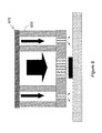
- FIG. 1 schematically shows a conventional nozzle for depositing a film
- FIG. 2A illustrates printed profile of the nozzle of FIG. 1 ;
- FIG. 2B illustrates the desired printed profile
- FIG. 3 shows lateral contamination caused by the conventional techniques
- FIG. 4 shows a multipore nozzle according to one embodiment of the disclosure
- FIGS. 5A-5C show several exemplary pore patterns
- FIGS. 6A-6C show complex pore patterns according to another embodiment of the disclosure.
- FIG. 7 illustrates an exemplary array of multipore nozzles
- FIG. 8 shows an embodiment of the disclosure having auxiliary gas streams for a fluid curtain
- FIG. 9 illustrates a multipore assembly with a gas curtain according to one embodiment of the disclosure.
- FIG. 10 is a cross-sectional view of the interface plate of FIG. 9 ;
- FIG. 11 shows a multipore nozzle with a thermal shutter according to another embodiment of the disclosure.
- FIG. 12 shows the multipore nozzle of FIG. 11 with the heater turned off
- FIG. 13 shows an exemplary nozzle having multiple orifices (or pores) for a fluid curtain
- FIG. 14 shows an exemplary nozzle with apertures for forming a fluid curtain
- FIG. 15 shows another exemplary discharge structure having multipore nozzles with two fluid ducts.
- FIG. 16 shows an exemplary embodiment in which the micropores provide overlapping deposits.
- Patterning of organic thin film is useful in variety of applications, including fabrication of light emitting displays. This is critical for OLED displays in particular because such displays require fabricating a number of patterned layers on a substrate. Each layer defines one of the colors: red, green and blue in each full color pixel.
- the patterning is performed using shadow mask evaporation.
- the shadow mask process is expensive and labor intensive. It is also prone to error and believed to be applicable only to relatively small areas.
- the disclosed embodiments overcome the deficiencies of the conventional techniques by providing a method and apparatus for depositing patterned organic thin films at low cost over large areas that further offer good uniformity over the target printed area and, where required, sharp edge profiles. While the disclosure is described in the context of using a carrier gas to communicate organic vapor material, it should be noted that the disclosed principles are not limited to organic vapor material and can apply to all printing methods in which a carrier medium is used to convey the deposition material to a destination substrate.
- the disclosure relates to a structure for depositing a film of substantially uniform thickness by receiving a carrier gas stream containing organic vapor material at a nozzle, distributing the carrier gas stream into a plurality of sub-streams at a microscale distributor (interchangeably, micron-scale showerhead) and directing the sub-streams through a plurality of micropores onto a substrate.
- the substrate having a lower temperature relative to the carrier gas stream causes condensation of the organic vapor material.
- the micropores can be organized to such that the vapor stream from each micropore simultaneously delivers an overlapping deposit of organic material on the substrate.
- the cross section of the deposit from a single microscale distributor can have a continuous, non-zero cross section that can be controlled through the proper engineering of the size, shape and pattern of the micropores.
- multiple vapor streams (or sub-streams) are at least partially merged to form a uniform deposited film.
- FIG. 1 schematically shows a conventional nozzle for depositing film.
- a stream of heated carrier gas is used to convey vaporized organic material.
- stream 110 represents a carrier gas containing vaporized organic material.
- the vaporized organic material carried in stream 110 is deposited on the top surface of substrate 130 to form a layer of film 115 .
- the conduit for conveying stream 110 to substrate 130 is schematically shown by walls 120 .
- vaporized organic material can be transported through a tube and out of nozzle 125 .
- substrate 130 is moved relative to nozzle 125 in order to deposit a desired pattern.
- Typical deposited film thicknesses range from between 10 nm to 200 nm when applied to OLED applications; however, there are no fundamental limits on the range of deposited film thicknesses when utilizing this technique.
- the single orifice nozzle 125 produces an approximately Gaussian shaped film profile as shown in FIG. 2A .
- the Gaussian shaped film profile typically does not have a uniform thickness over the target print region (unless the target print region is confined to a very narrow portion in the middle of the deposited area, which is usually impractical.) Multiple overlapping passes are needed with a very narrow print stream to approximate a flat region with sharp sidewalls (profiled edge) as shown in FIG. 2B .
- Such overlapping techniques are slow, expensive and prone to error given the tight mechanical alignment and tolerance required. It is also difficult to create a print stream that is sufficiently narrow to get sharp edge profiles at the edge of the printed region.
- FIG. 4 shows a multipore nozzle according to one embodiment of the disclosure.
- gas stream 410 is a hot gas carrying organic vapor material to be deposited on substrate 430 .
- Gas steam 410 is transported through conduit 420 to multipore nozzle 425 .
- Multipore nozzle 425 divides stream 410 to multiple sub-streams 412 .
- Each sub-stream 412 includes the carrier gas and vapor organic material.
- Sub-streams 412 deposit film layer 415 on substrate 430 .
- Film layer 415 has the desired profiled edges.
- Film 415 also has a substantially uniform thickness.
- multipore nozzle 425 prevents lateral contamination of organic vapor material across the substrate.
- the multipore nozzle can be fabricated using conventional techniques.
- the multipore nozzle was fabricated using MEMS fabrication techniques by forming very small pore (orifice) arrays and by depositing very small features.
- the pores and the features typically have a diameter of between 1-10 ⁇ m, though pore sizes of up to 100 ⁇ m are possible.
- the small, micron-scale size of the pores enable excellent film deposit uniformity and profiled edges (sharp sidewall).
- FIGS. 5A-5C show several exemplary pore patterns.
- the circular pores are arranged in an array.
- the multipore nozzle of FIG. 5A includes surface 510 , having fabricated therein pores 512 .
- Pores 512 are circular in shape and are arranged symmetrically about the nozzle.
- pores 514 are rectangular in shape and in FIG. 5C , rectangular pore 516 is supplemented by semi-circular pores 518 on each side.
- FIGS. 5A-5C illustrates that the shape of the pores can be designed to accommodate a number of shapes and orientations to accommodate different engineered deposited patterns and related film cross sections.
- the nozzles of FIGS. 5A-5C can be fabricated using conventional fabrication techniques such as MEMS.
- FIGS. 6A-6C show more complex pore patterns of multipore nozzles.
- FIG. 6 shows patterns of connected pores, having circular ( FIG. 6A ), rectangular ( FIG. 6B ) or complex ( FIG. 6C ) shapes. The shapes can be designed to provide different patterns and desired film cross sections.
- FIG. 7 illustrates an exemplary array of multipore nozzles.
- substrate 730 is positioned across an array of multipore nozzles 725 which deposit discrete films 715 from stream 710 .
- Stream 710 can have a hot carrier gas containing vaporized organic material.
- Each deposited film segment has a profiled edge and a substantially uniform thickness.
- Conduits 720 can be integrated with the multipore array or can be separate. In another implementation of the disclosure, conduits 720 may be eliminated entirely.
- the multipore nozzles are designed as interface plates and are removably coupled to a discharge conduit. Several multipore nozzles can be arranged to form an array of nozzles. The neighboring multi-nozzle pores in the array need not have identical shapes.
- FIG. 8 shows an embodiment of the disclosure having auxiliary gas streams.
- gas streams are positioned near the multipore nozzle in order to further rectify the shape of the vapor deposition.
- the auxiliary gas streams form an air curtain about the hot gas stream and further prevent lateral dissemination of organic vapor material.
- the auxiliary gas streams also help refining the profiled edge and the thickness of the deposited material.
- first gas stream 810 defines a hot gas stream carrying vaporized organic material therein.
- the vaporized organic material can be ink composed for OLED application.
- Gas stream 810 can have a temperature in the range of about 150° C. to 450° C., with 300° C. being typical.
- Gas stream 810 is directed to nozzles 825 .
- Nozzle 825 includes several micropores which divide gas stream 810 into a corresponding number of sub-streams. Each sub-stream carries a quantity of vaporized organic material. The sub-streams are then directed to substrate 830 .
- Substrate 830 can have a temperature lower than that of the first gas stream, allowing the vaporized organic material to condense on the surface thereof.
- auxiliary gas stream 850 is directed through corresponding micropores of nozzle 825 to form auxiliary sub-streams 855 .
- the auxiliary sub-streams can have a lower temperature than gas stream 810 and may contain no vapor organic material.
- the auxiliary gas stream can be, for example, a noble gas.
- auxiliary gas streams 855 can form a fluid (or gas) curtain about the target deposition area.
- the fluid curtain can form a profiled edge and a substantially uniform thickness for the condensed organic vapor material 815 .
- the cool gas curtain also prevents lateral spreading of the organic vapor material.
- FIG. 9 illustrates a multipore nozzle with a gas curtain according to one embodiment of the disclosure.
- the embodiment of FIG. 9 is substantially similar to that of FIG. 8 , except for the addition of interface plate 970 above conduit 920 .
- FIG. 10 is a cross-sectional view of the interface plate of FIG. 9 .
- auxiliary gas inlet 1072 which forms the fluid curtain is offset from hot carrier gas inlet 1074 .
- the hot carrier gas inlet contains organic vapor material and can have a substantially higher temperature than the auxiliary gas.
- Inlets 1072 and 1074 can be fabricated easily on surface 1070 using techniques such as mechanical milling or chemical etching.
- the inlets 1072 and 1074 on interface plate 1070 can be replicated or reconfigured to produce multipore discharge nozzles or arrays thereof.
- gas delivery system can be reduced to a simple supply line (or conduit) having two inlets.
- a first inlet delivers cool auxiliary gas for the fluid curtain and the second inlet delivers hot carrier gas containing organic vapor material.
- the interface plate provides a cost-efficient means for integrating the first and second inlet streams with a multi-nozzle discharge device.
- FIG. 11 shows a multipore nozzle with a thermal shutter according to another embodiment of the disclosure.
- element heating units 1160 are added to multipore nozzle 1125 .
- the heaters When the heaters are turned on, the pores are heated and hot gas 1110 is transmitted through the nozzle as shown by arrows 1155 .
- the organic vapor material condenses on the interior surfaces of the pores and the flow is obstructed.
- FIG. 12 shows pores of nozzle 1225 are obstructed after the hot organic vapor condenses inside the cool pores.
- an elemental heater can be effective for rapidly heating and cooling the system. Additional means, such as heat sink (not shown) can be added to the system to provide for faster cooling.
- the heating means can provide one or more of convection, conduction and/or radiation heating.
- a controller can be used.
- the controller can have one or more microprocessor circuits connected to one or more memory circuits.
- a flow regulator can be incorporated in the system to communicate with the controller.
- the flow regulator can optionally increase or decrease the hot gas flow rate ( 1110 in FIG. 11 ) according to whether heaters 1160 are on or off.
- the memory circuit can contain instructions for running the processor circuit and for starting and stopping the heater and/or the regulator.
- the flow of organic vapor material through the nozzles can be modulated.
- the heater When the heater is on, the material flows through the micropores without condensing on the micropore walls.
- the heater is off (with optional support from a heat sink), the micropores are cool enough that the material condenses on the walls instead of passing through.
- a nozzle heater and the fluid curtain can be used conjunctively to further control deposition thickness and profile.
- the fluid curtain can be activated only when the heater is on to further enhance deposition profile.
- Both the nozzle heater and the fluid curtain can be combined with a multipore nozzle to provide even more accuracy and control over film deposition profile.
- FIG. 13 shows an exemplary nozzle having multiple orifices for a fluid curtain.
- FIG. 13 A shows structure 1310 having circular nozzle 1320 at the center thereof and pores 1330 distributed around the nozzle.
- nozzle 1320 has one outlet port and pores 1330 provide a fluid curtain to the organic vapor film deposited through structure 1310 .
- a heater may optionally be added to structure 1310 .
- nozzle 1320 can be replaced with a multipore nozzle according to the instant disclosure. At least two micropores 1330 can be connected by a cavity to provide a different fluid curtain profile as shown with reference to FIG. 6 .
- FIG. 14 shows another exemplary nozzle 1410 with apertures for forming a fluid curtain.
- circular nozzle 1420 is positioned between fluid ducts 1430 .
- the organic vapor material which is conveyed through nozzle 1420 is surrounded by a fluid curtain provided by ducts 1430 .
- the exemplary structure shown in FIG. 14 can be replicated to form a large array containing multiple nozzles 1420 surrounded by ducts 1430 .
- FIG. 15 shows exemplary discharge structure 1510 having multipore nozzles 1520 and ducts 1530 .
- Ducts 1530 form a fluid curtain which delimits vapor organic material dispersion beyond a targeted print region.
- discharge structure 1510 can be formed in an array to provide for large area deposition.
- a heating apparatus may further be added to the embodiment of FIG. 15 .
- pores 1520 need not be circular and can assume any shape or form to accommodate the printing requirements.
- FIG. 16 shows an exemplary embodiment in which the micropores provide overlapping deposits.
- hot carrier gas stream 1605 is directed through nozzle 1610 to microscale distributor 1620 .
- Nozzle 1610 and distributor 1620 can be integrated into one unit. Alternatively, they can be built separately so that different distributors can be assembled to different nozzles.
- Microscale distributor 1620 distributes stream 1605 into a plurality of sub-streams through a plurality of micropores 1630 .
- Micropores 1630 can be organized such that the vapor stream from each micropore 1630 simultaneously delivers an overlapping deposit 1640 to substrate 1650 .
- the cross section of the deposit from a single microscale distributor has a continuous, non-zero cross section 1635 that can be controlled through the design of the size, shape and pattern of micropores 1630 .
- the organic vapor streams form film 1640 which has substantially uniform thickness.
- FIG. 16 overcomes many of the deficiencies of the conventional methods by replacing a single continuous orifice nozzle by a plurality of microscale orifices (which may not necessarily be circular). Positioning a fluid curtain at the nozzle can further refine the edges of deposit layer 1640 according to the embodiments disclosed above.
Landscapes
- Chemical & Material Sciences (AREA)
- Engineering & Computer Science (AREA)
- Chemical Kinetics & Catalysis (AREA)
- Materials Engineering (AREA)
- Mechanical Engineering (AREA)
- Metallurgy (AREA)
- Organic Chemistry (AREA)
- Manufacturing & Machinery (AREA)
- General Chemical & Material Sciences (AREA)
- Physical Vapour Deposition (AREA)
- Electroluminescent Light Sources (AREA)
- Treating Waste Gases (AREA)
Abstract
Description
Claims (19)
Priority Applications (2)
| Application Number | Priority Date | Filing Date | Title |
|---|---|---|---|
| US12/772,184 US8808799B2 (en) | 2009-05-01 | 2010-05-01 | Method and apparatus for organic vapor printing |
| US14/446,109 US20140331932A1 (en) | 2009-05-01 | 2014-07-29 | Method and Apparatus for Organic Vapor Printing |
Applications Claiming Priority (2)
| Application Number | Priority Date | Filing Date | Title |
|---|---|---|---|
| US17494309P | 2009-05-01 | 2009-05-01 | |
| US12/772,184 US8808799B2 (en) | 2009-05-01 | 2010-05-01 | Method and apparatus for organic vapor printing |
Related Child Applications (1)
| Application Number | Title | Priority Date | Filing Date |
|---|---|---|---|
| US14/446,109 Division US20140331932A1 (en) | 2009-05-01 | 2014-07-29 | Method and Apparatus for Organic Vapor Printing |
Publications (2)
| Publication Number | Publication Date |
|---|---|
| US20110008541A1 US20110008541A1 (en) | 2011-01-13 |
| US8808799B2 true US8808799B2 (en) | 2014-08-19 |
Family
ID=43032816
Family Applications (2)
| Application Number | Title | Priority Date | Filing Date |
|---|---|---|---|
| US12/772,184 Active 2032-05-13 US8808799B2 (en) | 2009-05-01 | 2010-05-01 | Method and apparatus for organic vapor printing |
| US14/446,109 Abandoned US20140331932A1 (en) | 2009-05-01 | 2014-07-29 | Method and Apparatus for Organic Vapor Printing |
Family Applications After (1)
| Application Number | Title | Priority Date | Filing Date |
|---|---|---|---|
| US14/446,109 Abandoned US20140331932A1 (en) | 2009-05-01 | 2014-07-29 | Method and Apparatus for Organic Vapor Printing |
Country Status (6)
| Country | Link |
|---|---|
| US (2) | US8808799B2 (en) |
| EP (1) | EP2425470A2 (en) |
| JP (1) | JP2012525505A (en) |
| KR (1) | KR101441737B1 (en) |
| CN (1) | CN102414863B (en) |
| WO (1) | WO2010127328A2 (en) |
Cited By (2)
| Publication number | Priority date | Publication date | Assignee | Title |
|---|---|---|---|---|
| US20140331932A1 (en) * | 2009-05-01 | 2014-11-13 | Kateeva, Inc. | Method and Apparatus for Organic Vapor Printing |
| US11401606B2 (en) | 2017-07-28 | 2022-08-02 | Boe Technology Group Co., Ltd. | Coating nozzle, coating device and corresponding coating method |
Families Citing this family (39)
| Publication number | Priority date | Publication date | Assignee | Title |
|---|---|---|---|---|
| US8986780B2 (en) | 2004-11-19 | 2015-03-24 | Massachusetts Institute Of Technology | Method and apparatus for depositing LED organic film |
| US8128753B2 (en) | 2004-11-19 | 2012-03-06 | Massachusetts Institute Of Technology | Method and apparatus for depositing LED organic film |
| US8556389B2 (en) | 2011-02-04 | 2013-10-15 | Kateeva, Inc. | Low-profile MEMS thermal printhead die having backside electrical connections |
| CN101754859B (en) * | 2007-06-14 | 2012-05-30 | 麻省理工学院 | Method and apparatus for depositing films |
| US8383202B2 (en) | 2008-06-13 | 2013-02-26 | Kateeva, Inc. | Method and apparatus for load-locked printing |
| US9604245B2 (en) | 2008-06-13 | 2017-03-28 | Kateeva, Inc. | Gas enclosure systems and methods utilizing an auxiliary enclosure |
| US8899171B2 (en) | 2008-06-13 | 2014-12-02 | Kateeva, Inc. | Gas enclosure assembly and system |
| US10434804B2 (en) | 2008-06-13 | 2019-10-08 | Kateeva, Inc. | Low particle gas enclosure systems and methods |
| US9048344B2 (en) | 2008-06-13 | 2015-06-02 | Kateeva, Inc. | Gas enclosure assembly and system |
| US11975546B2 (en) | 2008-06-13 | 2024-05-07 | Kateeva, Inc. | Gas enclosure assembly and system |
| US12018857B2 (en) | 2008-06-13 | 2024-06-25 | Kateeva, Inc. | Gas enclosure assembly and system |
| US12064979B2 (en) | 2008-06-13 | 2024-08-20 | Kateeva, Inc. | Low-particle gas enclosure systems and methods |
| US20100188457A1 (en) * | 2009-01-05 | 2010-07-29 | Madigan Connor F | Method and apparatus for controlling the temperature of an electrically-heated discharge nozzle |
| US20110097495A1 (en) * | 2009-09-03 | 2011-04-28 | Universal Display Corporation | Organic vapor jet printing with chiller plate |
| WO2012138366A1 (en) | 2011-04-08 | 2012-10-11 | Kateeva, Inc. | Method and apparatus for printing using a facetted drum |
| US9120344B2 (en) * | 2011-08-09 | 2015-09-01 | Kateeva, Inc. | Apparatus and method for control of print gap |
| KR20190101506A (en) | 2011-08-09 | 2019-08-30 | 카티바, 인크. | Face-down printing apparatus and method |
| JP2015004078A (en) * | 2011-10-18 | 2015-01-08 | 東京エレクトロン株式会社 | Film forming apparatus and film forming method |
| CN107264083B (en) * | 2013-10-02 | 2019-11-19 | 科迪华公司 | Apparatus and method for controlling printing gap |
| WO2015100375A1 (en) | 2013-12-26 | 2015-07-02 | Kateeva, Inc. | Thermal treatment of electronic devices |
| WO2015112454A1 (en) | 2014-01-21 | 2015-07-30 | Kateeva, Inc. | Apparatus and techniques for electronic device encapsulation |
| KR102850075B1 (en) | 2014-04-30 | 2025-08-25 | 카티바, 인크. | Gas cushion apparatus and techniques for substrate coating |
| CN105239038B (en) * | 2014-06-09 | 2017-12-05 | 华中科技大学 | A kind of organic vapors film formation device and its film build method using figure nozzle |
| US11267012B2 (en) | 2014-06-25 | 2022-03-08 | Universal Display Corporation | Spatial control of vapor condensation using convection |
| EP2960059B1 (en) | 2014-06-25 | 2018-10-24 | Universal Display Corporation | Systems and methods of modulating flow during vapor jet deposition of organic materials |
| US11220737B2 (en) * | 2014-06-25 | 2022-01-11 | Universal Display Corporation | Systems and methods of modulating flow during vapor jet deposition of organic materials |
| KR101674615B1 (en) * | 2015-05-14 | 2016-11-09 | 주식회사 아바코 | Depositon apparatus |
| US10566534B2 (en) | 2015-10-12 | 2020-02-18 | Universal Display Corporation | Apparatus and method to deliver organic material via organic vapor-jet printing (OVJP) |
| CN105457843A (en) * | 2016-01-18 | 2016-04-06 | 武汉华星光电技术有限公司 | Photoresist coating device and phtoresist coating method |
| JP2017018951A (en) * | 2016-07-28 | 2017-01-26 | カティーバ, インコーポレイテッド | Device and method for control of print gap |
| CN112941465A (en) * | 2016-07-29 | 2021-06-11 | 环球展览公司 | Deposition nozzle |
| CN106903996B (en) * | 2017-03-09 | 2020-05-29 | 京东方科技集团股份有限公司 | printing equipment |
| US11201288B2 (en) * | 2017-05-26 | 2021-12-14 | Universal Display Corporation | Generalized organic vapor jet depositor capable of high resolution printing and method for OVJP printing |
| US10998531B2 (en) * | 2017-12-12 | 2021-05-04 | Universal Display Corporation | Segmented OVJP print bar |
| CN111023317B (en) * | 2019-12-10 | 2021-09-17 | 陈巍 | Dry steam conveying spray pipe assembly for leading to air conditioner humidifying mechanism |
| WO2022097787A1 (en) * | 2020-11-06 | 2022-05-12 | 엘지전자 주식회사 | Inkjet head device |
| CN113522562A (en) * | 2021-07-23 | 2021-10-22 | 广东喜玛拉雅氢能科技有限公司 | A spraying equipment and membrane electrode spraying system for customizing spraying area |
| KR102575677B1 (en) * | 2023-01-04 | 2023-09-06 | 주식회사 디스닉스 | Plasma Etching Apparatus for Etching Multiple Composite Materials |
| CN118507420B (en) * | 2024-04-30 | 2025-09-05 | 北京海炬科技有限公司 | A pneumatic mass transfer device and method based on a single-head multi-hole array |
Citations (120)
| Publication number | Priority date | Publication date | Assignee | Title |
|---|---|---|---|---|
| US4238807A (en) | 1977-12-28 | 1980-12-09 | Ing. C. Olivetti & C., S.P.A. | Non-impact printing device |
| US4751531A (en) | 1986-03-27 | 1988-06-14 | Fuji Xerox Co., Ltd. | Thermal-electrostatic ink jet recording apparatus |
| US5116148A (en) | 1986-08-27 | 1992-05-26 | Hitachi, Ltd. | Heat transfer ink sheet having a precoating layer which is thermally transferred prior to sublimation of an ink dye |
| US5155502A (en) | 1989-01-13 | 1992-10-13 | Canon Kabushiki Kaisha | Ink-jet cartridge |
| US5172139A (en) | 1989-05-09 | 1992-12-15 | Ricoh Company, Ltd. | Liquid jet head for gradation recording |
| US5202659A (en) | 1984-04-16 | 1993-04-13 | Dataproducts, Corporation | Method and apparatus for selective multi-resonant operation of an ink jet controlling dot size |
| US5247190A (en) | 1989-04-20 | 1993-09-21 | Cambridge Research And Innovation Limited | Electroluminescent devices |
| US5405710A (en) | 1993-11-22 | 1995-04-11 | At&T Corp. | Article comprising microcavity light sources |
| US5574485A (en) | 1994-10-13 | 1996-11-12 | Xerox Corporation | Ultrasonic liquid wiper for ink jet printhead maintenance |
| US5623292A (en) | 1993-12-17 | 1997-04-22 | Videojet Systems International, Inc. | Temperature controller for ink jet printing |
| US5703436A (en) | 1994-12-13 | 1997-12-30 | The Trustees Of Princeton University | Transparent contacts for organic devices |
| US5707745A (en) | 1994-12-13 | 1998-01-13 | The Trustees Of Princeton University | Multicolor organic light emitting devices |
| US5731828A (en) | 1994-10-20 | 1998-03-24 | Canon Kabushiki Kaisha | Ink jet head, ink jet head cartridge and ink jet apparatus |
| US5781210A (en) | 1995-02-17 | 1998-07-14 | Sony Corporation | Recording method and recording solution |
| US5801721A (en) | 1994-09-09 | 1998-09-01 | Signtech U.S.A. Ltd. | Apparatus for producing an image on a first side of a substrate and a mirror image on a second side of the substrate |
| US5834893A (en) | 1996-12-23 | 1998-11-10 | The Trustees Of Princeton University | High efficiency organic light emitting devices with light directing structures |
| US5844363A (en) | 1997-01-23 | 1998-12-01 | The Trustees Of Princeton Univ. | Vacuum deposited, non-polymeric flexible organic light emitting devices |
| US5865860A (en) | 1997-06-20 | 1999-02-02 | Imra America, Inc. | Process for filling electrochemical cells with electrolyte |
| US5947022A (en) | 1997-11-07 | 1999-09-07 | Speedline Technologies, Inc. | Apparatus for dispensing material in a printer |
| US5956051A (en) | 1997-05-29 | 1999-09-21 | Pitney Bowes Inc. | Disabling a mailing machine when a print head is not installed |
| KR100232852B1 (en) | 1997-10-15 | 1999-12-01 | 윤종용 | Inkjet Printer Head and Manufacturing Method Thereof |
| US6013982A (en) | 1996-12-23 | 2000-01-11 | The Trustees Of Princeton University | Multicolor display devices |
| US6065825A (en) | 1997-11-13 | 2000-05-23 | Eastman Kodak Company | Printer having mechanically-assisted ink droplet separation and method of using same |
| US6087196A (en) | 1998-01-30 | 2000-07-11 | The Trustees Of Princeton University | Fabrication of organic semiconductor devices using ink jet printing |
| US6086195A (en) | 1998-09-24 | 2000-07-11 | Hewlett-Packard Company | Filter for an inkjet printhead |
| US6086196A (en) | 1995-04-14 | 2000-07-11 | Sony Corporation | Printing device |
| US6086679A (en) | 1997-10-24 | 2000-07-11 | Quester Technology, Inc. | Deposition systems and processes for transport polymerization and chemical vapor deposition |
| US6091195A (en) | 1997-02-03 | 2000-07-18 | The Trustees Of Princeton University | Displays having mesa pixel configuration |
| US6097147A (en) | 1998-09-14 | 2000-08-01 | The Trustees Of Princeton University | Structure for high efficiency electroluminescent device |
| US6095630A (en) | 1997-07-02 | 2000-08-01 | Sony Corporation | Ink-jet printer and drive method of recording head for ink-jet printer |
| US6189989B1 (en) | 1993-04-12 | 2001-02-20 | Canon Kabushiki Kaisha | Embroidering using ink jet printing apparatus |
| US6250747B1 (en) | 1999-01-28 | 2001-06-26 | Hewlett-Packard Company | Print cartridge with improved back-pressure regulation |
| US6294398B1 (en) | 1999-11-23 | 2001-09-25 | The Trustees Of Princeton University | Method for patterning devices |
| US6303238B1 (en) | 1997-12-01 | 2001-10-16 | The Trustees Of Princeton University | OLEDs doped with phosphorescent compounds |
| US6312083B1 (en) | 1999-12-20 | 2001-11-06 | Xerox Corporation | Printhead assembly with ink monitoring system |
| US20010045973A1 (en) | 2000-01-11 | 2001-11-29 | Eastman Kodak Company | Assisted drop-on-demand inkjet printer |
| US6326224B1 (en) | 1998-04-27 | 2001-12-04 | Motorola, Inc. | Method of purifying a primary color generated by an OED |
| US6337102B1 (en) | 1997-11-17 | 2002-01-08 | The Trustees Of Princeton University | Low pressure vapor phase deposition of organic thin films |
| US20020008732A1 (en) | 2000-07-20 | 2002-01-24 | Moon Jae-Ho | Ink-jet printhead |
| JP2002069650A (en) | 2000-08-31 | 2002-03-08 | Applied Materials Inc | Vapor phase deposition method and apparatus, and semiconductor device manufacturing method and apparatus |
| US6431702B2 (en) | 1999-06-08 | 2002-08-13 | Hewlett-Packard Company | Apparatus and method using ultrasonic energy to fix ink to print media |
| US6444400B1 (en) | 1999-08-23 | 2002-09-03 | Agfa-Gevaert | Method of making an electroconductive pattern on a support |
| US6453810B1 (en) | 1997-11-07 | 2002-09-24 | Speedline Technologies, Inc. | Method and apparatus for dispensing material in a printer |
| US6460972B1 (en) | 2001-11-06 | 2002-10-08 | Eastman Kodak Company | Thermal actuator drop-on-demand apparatus and method for high frequency |
| US6472962B1 (en) | 2001-05-17 | 2002-10-29 | Institute Of Microelectronics | Inductor-capacitor resonant RF switch |
| US20020191063A1 (en) | 2000-08-30 | 2002-12-19 | Daniel Gelbart | Method for imaging with UV curable inks |
| US6498802B1 (en) | 1999-12-02 | 2002-12-24 | Electronics And Telecommunications Research Institute | Organic micro-cavity laser |
| US6513903B2 (en) | 2000-12-29 | 2003-02-04 | Eastman Kodak Company | Ink jet print head with capillary flow cleaning |
| US6548956B2 (en) | 1994-12-13 | 2003-04-15 | The Trustees Of Princeton University | Transparent contacts for organic devices |
| US6562405B2 (en) | 2001-09-14 | 2003-05-13 | University Of Delaware | Multiple-nozzle thermal evaporation source |
| US6576134B1 (en) | 1998-10-20 | 2003-06-10 | Erik Agner | Method for displacement chromatography |
| US6586763B2 (en) | 1996-06-25 | 2003-07-01 | Northwestern University | Organic light-emitting diodes and methods for assembly and emission control |
| US6601936B2 (en) | 2000-11-14 | 2003-08-05 | Cypress Semiconductor Corp. | Real time adaptive inkjet temperature regulation controller |
| US20030230980A1 (en) | 2002-06-18 | 2003-12-18 | Forrest Stephen R | Very low voltage, high efficiency phosphorescent oled in a p-i-n structure |
| US6666548B1 (en) | 2002-11-04 | 2003-12-23 | Eastman Kodak Company | Method and apparatus for continuous marking |
| US20040009304A1 (en) | 2002-07-09 | 2004-01-15 | Osram Opto Semiconductors Gmbh & Co. Ogh | Process and tool with energy source for fabrication of organic electronic devices |
| US20040048000A1 (en) | 2001-09-04 | 2004-03-11 | Max Shtein | Device and method for organic vapor jet deposition |
| US20040048183A1 (en) | 2002-06-10 | 2004-03-11 | Seiko Epson Corporation | Production method of toner, toner, and toner producing apparatus |
| US20040056244A1 (en) | 2002-09-23 | 2004-03-25 | Eastman Kodak Company | Device for depositing patterned layers in OLED displays |
| US20040062862A1 (en) | 2002-09-28 | 2004-04-01 | Ahn Seong Deok | Method and apparatus using large-area organic vapor deposition for formation of organic thin films or organic devices |
| US20040086631A1 (en) | 2002-10-25 | 2004-05-06 | Yu-Kai Han | Ink jet printing device and method |
| US20040115339A1 (en) * | 2002-09-19 | 2004-06-17 | Nobuyuki Ito | Method and apparatus for manufacturing organic EL display and color filter by ink jet method |
| US20040202794A1 (en) | 2003-04-11 | 2004-10-14 | Dainippon Screen Mfg. Co., Ltd. | Coating material applying method and coating material applying apparatus for applying a coating material to surfaces of prints, and a printing machine having the coating material applying apparatus |
| US6811896B2 (en) | 2002-07-29 | 2004-11-02 | Xerox Corporation | Organic light emitting device (OLED) with thick (100 to 250 nanometers) porphyrin buffer layer |
| US6824262B2 (en) | 2001-08-10 | 2004-11-30 | Seiko Epson Corporation | Ink set and ink jet recording method |
| US20050005848A1 (en) * | 2003-04-25 | 2005-01-13 | Shunpei Yamazaki | Apparatus for forming a film and an electroluminescence device |
| US6861800B2 (en) | 2003-02-18 | 2005-03-01 | Eastman Kodak Company | Tuned microcavity color OLED display |
| US20050087131A1 (en) * | 2003-10-23 | 2005-04-28 | Max Shtein | Method and apparatus for depositing material |
| US6896346B2 (en) | 2002-12-26 | 2005-05-24 | Eastman Kodak Company | Thermo-mechanical actuator drop-on-demand apparatus and method with multiple drop volumes |
| US6917159B2 (en) | 2003-08-14 | 2005-07-12 | Eastman Kodak Company | Microcavity OLED device |
| US20050190220A1 (en) | 2004-02-27 | 2005-09-01 | Lim Seong-Taek | Method of driving an ink-jet printhead |
| JP2005286069A (en) | 2004-03-29 | 2005-10-13 | Kyocera Corp | Gas nozzle, manufacturing method thereof, and thin film forming apparatus using the same |
| US20050255249A1 (en) | 2002-05-29 | 2005-11-17 | Dirk Schlatterbeck | Method for applying coatings to surfaces |
| US20060012290A1 (en) | 2004-07-15 | 2006-01-19 | Chang-Ho Kang | Mask frame assembly for depositing thin layer and organic light emitting display device manufactured using the mask frame assembly |
| US7023013B2 (en) | 2004-06-16 | 2006-04-04 | Eastman Kodak Company | Array of light-emitting OLED microcavity pixels |
| JP2006123551A (en) | 2004-10-29 | 2006-05-18 | Samsung Electronics Co Ltd | NOZZLE PLATE, INKJET PRINT HEAD HAVING THE SAME, AND METHOD FOR PRODUCING NOZZLE PLATE |
| US20060115585A1 (en) * | 2004-11-19 | 2006-06-01 | Vladimir Bulovic | Method and apparatus for depositing LED organic film |
| JP2006150900A (en) | 2004-12-01 | 2006-06-15 | Canon Inc | Liquid discharge head and manufacturing method thereof |
| US7077513B2 (en) | 2001-02-09 | 2006-07-18 | Seiko Epson Corporation | Ink jet recording apparatus, control and ink replenishing method executed in the same, ink supply system incorporated in the same, and method of managing ink amount supplied by the system |
| US20070040877A1 (en) | 2005-08-16 | 2007-02-22 | Fuji Photo Film Co., Ltd. | Ink supply device, ink jet recording apparatus and ink cartridge |
| US20070058010A1 (en) | 2005-09-14 | 2007-03-15 | Fuji Photo Film Co., Ltd. | Liquid ejection head and image forming apparatus |
| JP2007095343A (en) | 2005-09-27 | 2007-04-12 | Toppan Printing Co Ltd | Method for producing printed matter and printed matter |
| US20070098891A1 (en) | 2005-10-31 | 2007-05-03 | Eastman Kodak Company | Vapor deposition apparatus and method |
| US20070134512A1 (en) | 2005-12-13 | 2007-06-14 | Eastman Kodak Company | Electroluminescent device containing an anthracene derivative |
| US20070163497A1 (en) * | 2006-01-17 | 2007-07-19 | Eastman Kodak Company | Two-dimensional aperture array for vapor deposition |
| US7247394B2 (en) | 2004-05-04 | 2007-07-24 | Eastman Kodak Company | Tuned microcavity color OLED display |
| US20070253686A1 (en) * | 2000-03-16 | 2007-11-01 | Wendt Robert G | Nozzle-based, vapor-phase, plume delivery structure for use in production of thin-film deposition layer |
| JP2007299616A (en) | 2006-04-28 | 2007-11-15 | Toppan Printing Co Ltd | Method for manufacturing organic EL element and organic EL element |
| US20070286944A1 (en) | 2006-06-13 | 2007-12-13 | Itc Inc., Ltd. | Fabrication of full-color oled panel using micro-cavity structure |
| US20080044571A1 (en) * | 2006-06-27 | 2008-02-21 | First Solar, Inc. | System and method for deposition of a material on a substrate |
| US7374984B2 (en) | 2004-10-29 | 2008-05-20 | Randy Hoffman | Method of forming a thin film component |
| US7377616B2 (en) | 2004-09-09 | 2008-05-27 | Brother Kogyo Kabushiki Kaisha | Inkjet printer including discharger with cap |
| US20080152806A1 (en) * | 2006-12-22 | 2008-06-26 | Stephen Forrest | Organic vapor jet deposition using an exhaust |
| US20080174235A1 (en) | 2006-10-13 | 2008-07-24 | Samsung Sdi Co., Ltd. | Mask used to fabricate organic light-emitting diode (oled) display device, method of fabricating oled display device using the mask, oled display device fabricated using the mask, and method of fabricating the mask |
| US7406761B2 (en) | 2005-03-21 | 2008-08-05 | Honeywell International Inc. | Method of manufacturing vibrating micromechanical structures |
| US7410240B2 (en) | 2004-03-04 | 2008-08-12 | Fujifilm Corporation | Inkjet recording head and inkjet recording apparatus |
| US20080238310A1 (en) | 2007-03-30 | 2008-10-02 | Forrest Stephen R | OLED with improved light outcoupling |
| US7431435B2 (en) | 2004-08-06 | 2008-10-07 | Matthew Grant Lopez | Systems and methods for varying dye concentrations |
| US7431968B1 (en) | 2001-09-04 | 2008-10-07 | The Trustees Of Princeton University | Process and apparatus for organic vapor jet deposition |
| US20080311289A1 (en) | 2007-06-14 | 2008-12-18 | Vladimir Bulovic | Method and apparatus for controlling film deposition |
| US20090031579A1 (en) | 2007-07-31 | 2009-02-05 | Piatt Michael J | Micro-structured drying for inkjet printers |
| US20090045739A1 (en) | 2007-08-16 | 2009-02-19 | Sam-Il Kho | Organic light emitting diode display device and method of fabricating the same |
| US20090115706A1 (en) | 2007-11-05 | 2009-05-07 | Samsung Electronics Co., Ltd. | Organic light emitting diode display and method for manufacturing the same |
| US7530778B2 (en) | 2001-12-27 | 2009-05-12 | Coreflow Ltd. | High-Performance non-contact support platforms |
| US20090167162A1 (en) | 2007-12-28 | 2009-07-02 | Universal Display Corporation | Dibenzothiophene-containing materials in phosphorescent light emitting diodes |
| US20090220680A1 (en) | 2008-02-29 | 2009-09-03 | Winters Dustin L | Oled device with short reduction |
| US7603439B2 (en) | 2002-04-09 | 2009-10-13 | Akamai Technologies, Inc. | System for tiered distribution in a content delivery network |
| US7604439B2 (en) | 2004-04-14 | 2009-10-20 | Coreflow Scientific Solutions Ltd. | Non-contact support platforms for distance adjustment |
| US20100055810A1 (en) | 2008-09-01 | 2010-03-04 | Samsung Mobile Display Co.,Ltd. | Mask for thin film deposition and method of manufacturing oled using the same |
| US7677690B2 (en) | 2005-11-22 | 2010-03-16 | Fujifilm Corporation | Liquid ejection apparatus and liquid agitation method |
| US20100079513A1 (en) | 2008-09-26 | 2010-04-01 | Brother Kogyo Kabushiki Kaisha | Liquid-ejection apparatus |
| US20100171780A1 (en) | 2009-01-05 | 2010-07-08 | Kateeva, Inc. | Rapid Ink-Charging Of A Dry Ink Discharge Nozzle |
| US20100201749A1 (en) | 2008-06-13 | 2010-08-12 | Kateeva, Inc. | Method And Apparatus for Load-Locked Printing |
| US20100310424A1 (en) | 2003-12-05 | 2010-12-09 | Massachusetts Institute Of Technology | Organic materials able to detect analytes |
| US7857121B2 (en) | 2005-09-15 | 2010-12-28 | Coreflow Scientific Solutions Ltd. | System and method for enhancing conveying performance of conveyors |
| US20110008541A1 (en) | 2009-05-01 | 2011-01-13 | Kateeva, Inc. | Method and apparatus for organic vapor printing |
| US7883832B2 (en) | 2005-01-04 | 2011-02-08 | International Business Machines Corporation | Method and apparatus for direct referencing of top surface of workpiece during imprint lithography |
| US20110057171A1 (en) | 2006-12-28 | 2011-03-10 | Universal Display Corporation | Long lifetime Phosphorescent Organic Light Emitting Device (OLED) Structures |
| US7908885B2 (en) | 2004-11-08 | 2011-03-22 | New Way Machine Components, Inc. | Non-contact porous air bearing and glass flattening device |
| US20110293818A1 (en) | 2009-11-27 | 2011-12-01 | Kateeva Inc. | Method and Apparatus for Depositing A Film Using A Rotating Source |
Family Cites Families (14)
| Publication number | Priority date | Publication date | Assignee | Title |
|---|---|---|---|---|
| WO2000016406A1 (en) * | 1998-09-10 | 2000-03-23 | Mitsubishi Denki Kabushiki Kaisha | Semiconductor device |
| CN1398360A (en) * | 2000-11-27 | 2003-02-19 | 皇家菲利浦电子有限公司 | light conversion device |
| US6688798B2 (en) * | 2001-02-27 | 2004-02-10 | Incumed, Inc. | Adjustable locking mount and methods of use |
| US8535759B2 (en) * | 2001-09-04 | 2013-09-17 | The Trustees Of Princeton University | Method and apparatus for depositing material using a dynamic pressure |
| JP2005082880A (en) * | 2003-09-11 | 2005-03-31 | Shoka Kagi Kofun Yugenkoshi | Film deposition apparatus for organic el light emitting device |
| JP4816034B2 (en) * | 2005-12-01 | 2011-11-16 | パナソニック株式会社 | Processing method and processing apparatus |
| WO2007117698A2 (en) * | 2006-04-07 | 2007-10-18 | Qd Vision, Inc. | Composition including material, methods of depositing material, articles including same and systems for depositing material |
| US20080098891A1 (en) * | 2006-10-25 | 2008-05-01 | General Electric Company | Turbine inlet air treatment apparatus |
| US7799377B2 (en) * | 2006-12-07 | 2010-09-21 | Electronics And Telecommunications Research Institute | Organic/inorganic thin film deposition method |
| EP2116629A4 (en) * | 2007-02-28 | 2010-11-24 | Ulvac Inc | Deposition source, deposition apparatus and method for forming organic thin film |
| JP2009228091A (en) * | 2008-03-25 | 2009-10-08 | Canon Inc | Vapor deposition apparatus |
| KR101055606B1 (en) * | 2008-10-22 | 2011-08-10 | 한국과학기술원 | Organic dry jet printing head and printing apparatus and method using same |
| US8931431B2 (en) * | 2009-03-25 | 2015-01-13 | The Regents Of The University Of Michigan | Nozzle geometry for organic vapor jet printing |
| US8613496B2 (en) * | 2009-03-25 | 2013-12-24 | The Regents Of The University Of Michigan | Compact organic vapor jet printing print head |
-
2010
- 2010-05-01 EP EP10770473A patent/EP2425470A2/en not_active Withdrawn
- 2010-05-01 US US12/772,184 patent/US8808799B2/en active Active
- 2010-05-01 JP JP2012508807A patent/JP2012525505A/en active Pending
- 2010-05-01 WO PCT/US2010/033315 patent/WO2010127328A2/en not_active Ceased
- 2010-05-01 KR KR1020117027783A patent/KR101441737B1/en not_active Expired - Fee Related
- 2010-05-01 CN CN201080019410.0A patent/CN102414863B/en not_active Expired - Fee Related
-
2014
- 2014-07-29 US US14/446,109 patent/US20140331932A1/en not_active Abandoned
Patent Citations (137)
| Publication number | Priority date | Publication date | Assignee | Title |
|---|---|---|---|---|
| US4238807A (en) | 1977-12-28 | 1980-12-09 | Ing. C. Olivetti & C., S.P.A. | Non-impact printing device |
| US5202659A (en) | 1984-04-16 | 1993-04-13 | Dataproducts, Corporation | Method and apparatus for selective multi-resonant operation of an ink jet controlling dot size |
| US4751531A (en) | 1986-03-27 | 1988-06-14 | Fuji Xerox Co., Ltd. | Thermal-electrostatic ink jet recording apparatus |
| US5116148A (en) | 1986-08-27 | 1992-05-26 | Hitachi, Ltd. | Heat transfer ink sheet having a precoating layer which is thermally transferred prior to sublimation of an ink dye |
| US5155502A (en) | 1989-01-13 | 1992-10-13 | Canon Kabushiki Kaisha | Ink-jet cartridge |
| US5247190A (en) | 1989-04-20 | 1993-09-21 | Cambridge Research And Innovation Limited | Electroluminescent devices |
| US5172139A (en) | 1989-05-09 | 1992-12-15 | Ricoh Company, Ltd. | Liquid jet head for gradation recording |
| US6189989B1 (en) | 1993-04-12 | 2001-02-20 | Canon Kabushiki Kaisha | Embroidering using ink jet printing apparatus |
| US5405710A (en) | 1993-11-22 | 1995-04-11 | At&T Corp. | Article comprising microcavity light sources |
| US5623292A (en) | 1993-12-17 | 1997-04-22 | Videojet Systems International, Inc. | Temperature controller for ink jet printing |
| US5801721A (en) | 1994-09-09 | 1998-09-01 | Signtech U.S.A. Ltd. | Apparatus for producing an image on a first side of a substrate and a mirror image on a second side of the substrate |
| US5574485A (en) | 1994-10-13 | 1996-11-12 | Xerox Corporation | Ultrasonic liquid wiper for ink jet printhead maintenance |
| US5731828A (en) | 1994-10-20 | 1998-03-24 | Canon Kabushiki Kaisha | Ink jet head, ink jet head cartridge and ink jet apparatus |
| US5703436A (en) | 1994-12-13 | 1997-12-30 | The Trustees Of Princeton University | Transparent contacts for organic devices |
| US5707745A (en) | 1994-12-13 | 1998-01-13 | The Trustees Of Princeton University | Multicolor organic light emitting devices |
| US6548956B2 (en) | 1994-12-13 | 2003-04-15 | The Trustees Of Princeton University | Transparent contacts for organic devices |
| US5781210A (en) | 1995-02-17 | 1998-07-14 | Sony Corporation | Recording method and recording solution |
| US6086196A (en) | 1995-04-14 | 2000-07-11 | Sony Corporation | Printing device |
| US6586763B2 (en) | 1996-06-25 | 2003-07-01 | Northwestern University | Organic light-emitting diodes and methods for assembly and emission control |
| US5834893A (en) | 1996-12-23 | 1998-11-10 | The Trustees Of Princeton University | High efficiency organic light emitting devices with light directing structures |
| US6013982A (en) | 1996-12-23 | 2000-01-11 | The Trustees Of Princeton University | Multicolor display devices |
| US5844363A (en) | 1997-01-23 | 1998-12-01 | The Trustees Of Princeton Univ. | Vacuum deposited, non-polymeric flexible organic light emitting devices |
| US6091195A (en) | 1997-02-03 | 2000-07-18 | The Trustees Of Princeton University | Displays having mesa pixel configuration |
| US5956051A (en) | 1997-05-29 | 1999-09-21 | Pitney Bowes Inc. | Disabling a mailing machine when a print head is not installed |
| US5865860A (en) | 1997-06-20 | 1999-02-02 | Imra America, Inc. | Process for filling electrochemical cells with electrolyte |
| US6095630A (en) | 1997-07-02 | 2000-08-01 | Sony Corporation | Ink-jet printer and drive method of recording head for ink-jet printer |
| US6257706B1 (en) | 1997-10-15 | 2001-07-10 | Samsung Electronics Co., Ltd. | Micro injecting device and a method of manufacturing |
| KR100232852B1 (en) | 1997-10-15 | 1999-12-01 | 윤종용 | Inkjet Printer Head and Manufacturing Method Thereof |
| US6086679A (en) | 1997-10-24 | 2000-07-11 | Quester Technology, Inc. | Deposition systems and processes for transport polymerization and chemical vapor deposition |
| US5947022A (en) | 1997-11-07 | 1999-09-07 | Speedline Technologies, Inc. | Apparatus for dispensing material in a printer |
| US6453810B1 (en) | 1997-11-07 | 2002-09-24 | Speedline Technologies, Inc. | Method and apparatus for dispensing material in a printer |
| US6065825A (en) | 1997-11-13 | 2000-05-23 | Eastman Kodak Company | Printer having mechanically-assisted ink droplet separation and method of using same |
| US6337102B1 (en) | 1997-11-17 | 2002-01-08 | The Trustees Of Princeton University | Low pressure vapor phase deposition of organic thin films |
| US6303238B1 (en) | 1997-12-01 | 2001-10-16 | The Trustees Of Princeton University | OLEDs doped with phosphorescent compounds |
| US6087196A (en) | 1998-01-30 | 2000-07-11 | The Trustees Of Princeton University | Fabrication of organic semiconductor devices using ink jet printing |
| US6326224B1 (en) | 1998-04-27 | 2001-12-04 | Motorola, Inc. | Method of purifying a primary color generated by an OED |
| US6097147A (en) | 1998-09-14 | 2000-08-01 | The Trustees Of Princeton University | Structure for high efficiency electroluminescent device |
| US6086195A (en) | 1998-09-24 | 2000-07-11 | Hewlett-Packard Company | Filter for an inkjet printhead |
| US6576134B1 (en) | 1998-10-20 | 2003-06-10 | Erik Agner | Method for displacement chromatography |
| US6250747B1 (en) | 1999-01-28 | 2001-06-26 | Hewlett-Packard Company | Print cartridge with improved back-pressure regulation |
| US6431702B2 (en) | 1999-06-08 | 2002-08-13 | Hewlett-Packard Company | Apparatus and method using ultrasonic energy to fix ink to print media |
| US6444400B1 (en) | 1999-08-23 | 2002-09-03 | Agfa-Gevaert | Method of making an electroconductive pattern on a support |
| US6294398B1 (en) | 1999-11-23 | 2001-09-25 | The Trustees Of Princeton University | Method for patterning devices |
| US6468819B1 (en) | 1999-11-23 | 2002-10-22 | The Trustees Of Princeton University | Method for patterning organic thin film devices using a die |
| US6498802B1 (en) | 1999-12-02 | 2002-12-24 | Electronics And Telecommunications Research Institute | Organic micro-cavity laser |
| US6312083B1 (en) | 1999-12-20 | 2001-11-06 | Xerox Corporation | Printhead assembly with ink monitoring system |
| US20010045973A1 (en) | 2000-01-11 | 2001-11-29 | Eastman Kodak Company | Assisted drop-on-demand inkjet printer |
| US20070253686A1 (en) * | 2000-03-16 | 2007-11-01 | Wendt Robert G | Nozzle-based, vapor-phase, plume delivery structure for use in production of thin-film deposition layer |
| US20020008732A1 (en) | 2000-07-20 | 2002-01-24 | Moon Jae-Ho | Ink-jet printhead |
| US20020191063A1 (en) | 2000-08-30 | 2002-12-19 | Daniel Gelbart | Method for imaging with UV curable inks |
| JP2002069650A (en) | 2000-08-31 | 2002-03-08 | Applied Materials Inc | Vapor phase deposition method and apparatus, and semiconductor device manufacturing method and apparatus |
| US6601936B2 (en) | 2000-11-14 | 2003-08-05 | Cypress Semiconductor Corp. | Real time adaptive inkjet temperature regulation controller |
| US6513903B2 (en) | 2000-12-29 | 2003-02-04 | Eastman Kodak Company | Ink jet print head with capillary flow cleaning |
| US7077513B2 (en) | 2001-02-09 | 2006-07-18 | Seiko Epson Corporation | Ink jet recording apparatus, control and ink replenishing method executed in the same, ink supply system incorporated in the same, and method of managing ink amount supplied by the system |
| US6472962B1 (en) | 2001-05-17 | 2002-10-29 | Institute Of Microelectronics | Inductor-capacitor resonant RF switch |
| US6824262B2 (en) | 2001-08-10 | 2004-11-30 | Seiko Epson Corporation | Ink set and ink jet recording method |
| US20040048000A1 (en) | 2001-09-04 | 2004-03-11 | Max Shtein | Device and method for organic vapor jet deposition |
| US7431968B1 (en) | 2001-09-04 | 2008-10-07 | The Trustees Of Princeton University | Process and apparatus for organic vapor jet deposition |
| US7404862B2 (en) | 2001-09-04 | 2008-07-29 | The Trustees Of Princeton University | Device and method for organic vapor jet deposition |
| US20080299311A1 (en) | 2001-09-04 | 2008-12-04 | The Trustees Of Princeton University | Process and Apparatus for Organic Vapor Jet Deposition |
| US20080311296A1 (en) | 2001-09-04 | 2008-12-18 | The Trustees Of Princeton University | Device and Method for Organic Vapor Jet Deposition |
| US6982005B2 (en) | 2001-09-14 | 2006-01-03 | University Of Delaware | Multiple-nozzle thermal evaporation source |
| US6562405B2 (en) | 2001-09-14 | 2003-05-13 | University Of Delaware | Multiple-nozzle thermal evaporation source |
| US6460972B1 (en) | 2001-11-06 | 2002-10-08 | Eastman Kodak Company | Thermal actuator drop-on-demand apparatus and method for high frequency |
| US7530778B2 (en) | 2001-12-27 | 2009-05-12 | Coreflow Ltd. | High-Performance non-contact support platforms |
| US7603439B2 (en) | 2002-04-09 | 2009-10-13 | Akamai Technologies, Inc. | System for tiered distribution in a content delivery network |
| US20050255249A1 (en) | 2002-05-29 | 2005-11-17 | Dirk Schlatterbeck | Method for applying coatings to surfaces |
| US20040048183A1 (en) | 2002-06-10 | 2004-03-11 | Seiko Epson Corporation | Production method of toner, toner, and toner producing apparatus |
| US20030230980A1 (en) | 2002-06-18 | 2003-12-18 | Forrest Stephen R | Very low voltage, high efficiency phosphorescent oled in a p-i-n structure |
| US20040009304A1 (en) | 2002-07-09 | 2004-01-15 | Osram Opto Semiconductors Gmbh & Co. Ogh | Process and tool with energy source for fabrication of organic electronic devices |
| US6811896B2 (en) | 2002-07-29 | 2004-11-02 | Xerox Corporation | Organic light emitting device (OLED) with thick (100 to 250 nanometers) porphyrin buffer layer |
| US20040115339A1 (en) * | 2002-09-19 | 2004-06-17 | Nobuyuki Ito | Method and apparatus for manufacturing organic EL display and color filter by ink jet method |
| US6911671B2 (en) | 2002-09-23 | 2005-06-28 | Eastman Kodak Company | Device for depositing patterned layers in OLED displays |
| US20040056244A1 (en) | 2002-09-23 | 2004-03-25 | Eastman Kodak Company | Device for depositing patterned layers in OLED displays |
| US20040062862A1 (en) | 2002-09-28 | 2004-04-01 | Ahn Seong Deok | Method and apparatus using large-area organic vapor deposition for formation of organic thin films or organic devices |
| US20040086631A1 (en) | 2002-10-25 | 2004-05-06 | Yu-Kai Han | Ink jet printing device and method |
| US6666548B1 (en) | 2002-11-04 | 2003-12-23 | Eastman Kodak Company | Method and apparatus for continuous marking |
| US6896346B2 (en) | 2002-12-26 | 2005-05-24 | Eastman Kodak Company | Thermo-mechanical actuator drop-on-demand apparatus and method with multiple drop volumes |
| US6861800B2 (en) | 2003-02-18 | 2005-03-01 | Eastman Kodak Company | Tuned microcavity color OLED display |
| US20040202794A1 (en) | 2003-04-11 | 2004-10-14 | Dainippon Screen Mfg. Co., Ltd. | Coating material applying method and coating material applying apparatus for applying a coating material to surfaces of prints, and a printing machine having the coating material applying apparatus |
| US20050005848A1 (en) * | 2003-04-25 | 2005-01-13 | Shunpei Yamazaki | Apparatus for forming a film and an electroluminescence device |
| US6917159B2 (en) | 2003-08-14 | 2005-07-12 | Eastman Kodak Company | Microcavity OLED device |
| US20050087131A1 (en) * | 2003-10-23 | 2005-04-28 | Max Shtein | Method and apparatus for depositing material |
| US20100310424A1 (en) | 2003-12-05 | 2010-12-09 | Massachusetts Institute Of Technology | Organic materials able to detect analytes |
| US20050190220A1 (en) | 2004-02-27 | 2005-09-01 | Lim Seong-Taek | Method of driving an ink-jet printhead |
| US7410240B2 (en) | 2004-03-04 | 2008-08-12 | Fujifilm Corporation | Inkjet recording head and inkjet recording apparatus |
| JP2005286069A (en) | 2004-03-29 | 2005-10-13 | Kyocera Corp | Gas nozzle, manufacturing method thereof, and thin film forming apparatus using the same |
| US7604439B2 (en) | 2004-04-14 | 2009-10-20 | Coreflow Scientific Solutions Ltd. | Non-contact support platforms for distance adjustment |
| US7247394B2 (en) | 2004-05-04 | 2007-07-24 | Eastman Kodak Company | Tuned microcavity color OLED display |
| US7023013B2 (en) | 2004-06-16 | 2006-04-04 | Eastman Kodak Company | Array of light-emitting OLED microcavity pixels |
| EP1626103B1 (en) | 2004-07-15 | 2009-10-28 | Samsung Mobile Display Co., Ltd. | Mask frame assembly for depositing thin layer and organic light emitting display device manufactured using the mask frame assembly |
| US7802537B2 (en) | 2004-07-15 | 2010-09-28 | Samsung Mobile Display Co., Ltd. | Mask frame assembly for depositing thin layer and organic light emitting display device manufactured using the mask frame assembly |
| US20060012290A1 (en) | 2004-07-15 | 2006-01-19 | Chang-Ho Kang | Mask frame assembly for depositing thin layer and organic light emitting display device manufactured using the mask frame assembly |
| US7431435B2 (en) | 2004-08-06 | 2008-10-07 | Matthew Grant Lopez | Systems and methods for varying dye concentrations |
| US7377616B2 (en) | 2004-09-09 | 2008-05-27 | Brother Kogyo Kabushiki Kaisha | Inkjet printer including discharger with cap |
| JP2006123551A (en) | 2004-10-29 | 2006-05-18 | Samsung Electronics Co Ltd | NOZZLE PLATE, INKJET PRINT HEAD HAVING THE SAME, AND METHOD FOR PRODUCING NOZZLE PLATE |
| US7374984B2 (en) | 2004-10-29 | 2008-05-20 | Randy Hoffman | Method of forming a thin film component |
| US7908885B2 (en) | 2004-11-08 | 2011-03-22 | New Way Machine Components, Inc. | Non-contact porous air bearing and glass flattening device |
| US8128753B2 (en) | 2004-11-19 | 2012-03-06 | Massachusetts Institute Of Technology | Method and apparatus for depositing LED organic film |
| US20060115585A1 (en) * | 2004-11-19 | 2006-06-01 | Vladimir Bulovic | Method and apparatus for depositing LED organic film |
| JP2006150900A (en) | 2004-12-01 | 2006-06-15 | Canon Inc | Liquid discharge head and manufacturing method thereof |
| US7883832B2 (en) | 2005-01-04 | 2011-02-08 | International Business Machines Corporation | Method and apparatus for direct referencing of top surface of workpiece during imprint lithography |
| US7406761B2 (en) | 2005-03-21 | 2008-08-05 | Honeywell International Inc. | Method of manufacturing vibrating micromechanical structures |
| US7648230B2 (en) | 2005-08-16 | 2010-01-19 | Fujifilm Corporation | Ink supply device, ink jet recording apparatus and ink cartridge |
| US20070040877A1 (en) | 2005-08-16 | 2007-02-22 | Fuji Photo Film Co., Ltd. | Ink supply device, ink jet recording apparatus and ink cartridge |
| JP2007076168A (en) | 2005-09-14 | 2007-03-29 | Fujifilm Corp | Liquid ejection head and image forming apparatus |
| US20070058010A1 (en) | 2005-09-14 | 2007-03-15 | Fuji Photo Film Co., Ltd. | Liquid ejection head and image forming apparatus |
| US7857121B2 (en) | 2005-09-15 | 2010-12-28 | Coreflow Scientific Solutions Ltd. | System and method for enhancing conveying performance of conveyors |
| JP2007095343A (en) | 2005-09-27 | 2007-04-12 | Toppan Printing Co Ltd | Method for producing printed matter and printed matter |
| US20070098891A1 (en) | 2005-10-31 | 2007-05-03 | Eastman Kodak Company | Vapor deposition apparatus and method |
| US7677690B2 (en) | 2005-11-22 | 2010-03-16 | Fujifilm Corporation | Liquid ejection apparatus and liquid agitation method |
| US20070134512A1 (en) | 2005-12-13 | 2007-06-14 | Eastman Kodak Company | Electroluminescent device containing an anthracene derivative |
| US20070163497A1 (en) * | 2006-01-17 | 2007-07-19 | Eastman Kodak Company | Two-dimensional aperture array for vapor deposition |
| JP2007299616A (en) | 2006-04-28 | 2007-11-15 | Toppan Printing Co Ltd | Method for manufacturing organic EL element and organic EL element |
| US20070286944A1 (en) | 2006-06-13 | 2007-12-13 | Itc Inc., Ltd. | Fabrication of full-color oled panel using micro-cavity structure |
| US20080044571A1 (en) * | 2006-06-27 | 2008-02-21 | First Solar, Inc. | System and method for deposition of a material on a substrate |
| US20080174235A1 (en) | 2006-10-13 | 2008-07-24 | Samsung Sdi Co., Ltd. | Mask used to fabricate organic light-emitting diode (oled) display device, method of fabricating oled display device using the mask, oled display device fabricated using the mask, and method of fabricating the mask |
| US20080152806A1 (en) * | 2006-12-22 | 2008-06-26 | Stephen Forrest | Organic vapor jet deposition using an exhaust |
| US20110057171A1 (en) | 2006-12-28 | 2011-03-10 | Universal Display Corporation | Long lifetime Phosphorescent Organic Light Emitting Device (OLED) Structures |
| US20080238310A1 (en) | 2007-03-30 | 2008-10-02 | Forrest Stephen R | OLED with improved light outcoupling |
| US20080311307A1 (en) | 2007-06-14 | 2008-12-18 | Massachusetts Institute Of Technology | Method and apparatus for depositing films |
| US20080311289A1 (en) | 2007-06-14 | 2008-12-18 | Vladimir Bulovic | Method and apparatus for controlling film deposition |
| US20110267390A1 (en) | 2007-06-14 | 2011-11-03 | Massachusetts Institute Of Technology | Method and apparatus for depositing films |
| US20110181644A1 (en) | 2007-06-14 | 2011-07-28 | Massachusetts Institute Of Technology | Method and Apparatus for Controlling Film Deposition |
| US20080308037A1 (en) | 2007-06-14 | 2008-12-18 | Massachusetts Institute Of Technology | Method and apparatus for thermal jet printing |
| US20090031579A1 (en) | 2007-07-31 | 2009-02-05 | Piatt Michael J | Micro-structured drying for inkjet printers |
| US20090045739A1 (en) | 2007-08-16 | 2009-02-19 | Sam-Il Kho | Organic light emitting diode display device and method of fabricating the same |
| US20090115706A1 (en) | 2007-11-05 | 2009-05-07 | Samsung Electronics Co., Ltd. | Organic light emitting diode display and method for manufacturing the same |
| US20090167162A1 (en) | 2007-12-28 | 2009-07-02 | Universal Display Corporation | Dibenzothiophene-containing materials in phosphorescent light emitting diodes |
| US20090220680A1 (en) | 2008-02-29 | 2009-09-03 | Winters Dustin L | Oled device with short reduction |
| US20100201749A1 (en) | 2008-06-13 | 2010-08-12 | Kateeva, Inc. | Method And Apparatus for Load-Locked Printing |
| US20100055810A1 (en) | 2008-09-01 | 2010-03-04 | Samsung Mobile Display Co.,Ltd. | Mask for thin film deposition and method of manufacturing oled using the same |
| US20100079513A1 (en) | 2008-09-26 | 2010-04-01 | Brother Kogyo Kabushiki Kaisha | Liquid-ejection apparatus |
| US20100188457A1 (en) | 2009-01-05 | 2010-07-29 | Madigan Connor F | Method and apparatus for controlling the temperature of an electrically-heated discharge nozzle |
| US20100171780A1 (en) | 2009-01-05 | 2010-07-08 | Kateeva, Inc. | Rapid Ink-Charging Of A Dry Ink Discharge Nozzle |
| US20110008541A1 (en) | 2009-05-01 | 2011-01-13 | Kateeva, Inc. | Method and apparatus for organic vapor printing |
| US20110293818A1 (en) | 2009-11-27 | 2011-12-01 | Kateeva Inc. | Method and Apparatus for Depositing A Film Using A Rotating Source |
Non-Patent Citations (33)
| Title |
|---|
| A Notification of the First Office Action issued on Dec. 30, 2013, for the corresponding Chinese Patent Application CN 201312251402880. |
| C. Ducso, et al. "Porous Silicon Bulk Micromachining for Thermally Isolated Membrane Formation," Sensors and Actuators A, 1997, vol. 60, pp. 235-239. |
| C. Tsamis, et al. "Thermal Properties of Suspended Porous Micro-hotplates for Sensor Applications," Sensor and Actuators B, 2003, vol. 95, pp. 78-82. |
| Chen et al., "Ambient Environment Patterning of Organic Thin Films by a Second Generation Molecular Jet (MoJet) Printer," Progress Report 2006-2007, Oct. 2007, pp. 26-6; 26-7. |
| Chen et al., "Evaporative Deposition of Molecular Organics in Ambient with a Molecular Jet Printer," Digital Fabrication, Sep. 2006, pp. 63-65. |
| Chen, Jianglong, "Novel Patterning Techniques for Manufacturing Organic and Nanostructured Electronics," M.S. Materials Science and Engineering, Massachusetts Institute of Technology, 2003, pp. 1-206. |
| Chen, Jingkuang et al., "A High-Resolution Silicon Monolithic Nozzle Array for Inkjet Printing," IEEE Transactions on Electron Devices, vol. 44, No. 9, Sep. 1997, pp. 1401-1409. |
| Chin, Byung Doo, "Effective Hole Transport Layer Structure for Top Emitting Devices Based on Laser Transfer Patterning," Journal of Physics D: Applied Physics, 2007, vol. 40, pp. 5541-5546. |
| CN Office Action dated Dec. 17, 2010 issued for CN Patent Application 200880020151.6. |
| CN Office Action dated Jan. 12, 2011 issued for CN Patent Application 200880019990.6. |
| CN Office Action dated Oct. 12, 2010 issued for CN Patent Application 200880020197.8. |
| CN Second Office Action dated Jun. 22, 2011 issued for CN Patent Application 200880020197.8. |
| Elwenspoek et al., "Silicon Micromachining," Aug. 2004, Cambridge University, Cambridge, U.K. ISBN 0521607671. [Abstract]. |
| EP Examination Report dated Jul. 13, 2010 issued for EP Patent Application 08771084.4. |
| EP Examination Report dated Jul. 13, 2010 issued for EP Patent Application 08771094.3. |
| EP Examination Report dated Jul. 30, 2010 issued for EP Patent Application 08771068.7. |
| Forrest, Stephen R., "The Path to Ubiquitous and Low-cost Organic Electronic Appliances on Plastic," Nature, Apr. 29, 2004, vol. 428, 8 pages. |
| G.S. Chung, "Fabrication and Characterization of Micro-heaters with Low-power Consumption using SOI membrane and Trench Structures," Sensors and Actuators A, 2004, vol. 112, pp. 55-60. |
| Geffroy et al., "Organic Light-emitting Diode (OLED) Technology: Material Devices and Display Technologies," Polymer International, Jun. 2006, vol. 55, pp. 572-582 (Abstract Only). |
| Huang et al., "Reducing Blueshift of Viewing Angle for Top-Eimtting Organic Light-Emitting Devices," Dec. 6, 2008, 3 pages. |
| International Preliminary Report on Patentability issued on Dec. 17, 2009 for PCT Application No. PCT/US08/66975. |
| International Preliminary Report on Patentability issued on Dec. 17, 2009 for PCT Application No. PCT/US08/67002. |
| International Preliminary Report on Patentability issued on Dec. 7, 2009 for PCT Application No. PCT/US08/066991. |
| International Search Report and Written Opinion issued on Mar. 24, 2011 for PCT Application No. PCT/US10/058145. |
| International Search Report issued on Dec. 15, 2010 for PCT Application No. PCT/US10/020144. |
| International Search Report issued on Sep. 2, 2010 for PCT Application No. PCT/US10/033315. |
| J. C. Belmonte, et al. "High-temperature Low-power Performing Micromachined Suspended Micro-hotplate for Gas Sensing Applications<" Sensors and Actuators B, 2006, vol. 114, pp. 826-835. |
| J. Lee, et al. "Cavity Effects on Light Extraction in Organic Light emitting Devices," Applied Physics Letters, Jan. 24, 2008, vol. 92, No. 3, 5 pages. |
| J. Lee, et al. "Differential Scanning Calorimeter Based on Suspended Membrane Single Crystal Silicon Microhotplate," Journal of Microelectromechanical Systems, Dec. 2008, vol. 17, No. 6, pp. 1513-1525. |
| Leblanc et al., "Micromachined Printheads for the Evaporative Patterning of Organic Materials and Metals," Journal of Microelectromechanical Systems, Apr. 2007, vol. 16, No. 2, 7 pp. 1-139. |
| Lindermann et al., "Thermal Bubble Jet Printhead with Integrated Nozzle Plate," NIP20: International Conference on Digital Printing Technologies, Oct. 2004, pp.834-839. |
| S.H. Kim et al. "Fabrication and Characterization of co-planar type MEMS Structures on SiO2/Si3N4 Membrane for Gas Sensors with Dispensing Method Guided by Micromachined Wells," Journal of Eletroceramics, Jun. 27, 2005, vol. 17, No. 2-4, pp. 995-998. |
| Street et al., "Jet Printing of Active-Matrix TFT Backplanes for Displays and Sensors", IS&T Archiving, Dec. 2005, vol. 20, No. 5, 16 pages. |
Cited By (2)
| Publication number | Priority date | Publication date | Assignee | Title |
|---|---|---|---|---|
| US20140331932A1 (en) * | 2009-05-01 | 2014-11-13 | Kateeva, Inc. | Method and Apparatus for Organic Vapor Printing |
| US11401606B2 (en) | 2017-07-28 | 2022-08-02 | Boe Technology Group Co., Ltd. | Coating nozzle, coating device and corresponding coating method |
Also Published As
| Publication number | Publication date |
|---|---|
| CN102414863A (en) | 2012-04-11 |
| CN102414863B (en) | 2015-06-03 |
| US20110008541A1 (en) | 2011-01-13 |
| WO2010127328A2 (en) | 2010-11-04 |
| KR20120004532A (en) | 2012-01-12 |
| US20140331932A1 (en) | 2014-11-13 |
| JP2012525505A (en) | 2012-10-22 |
| KR101441737B1 (en) | 2014-09-17 |
| WO2010127328A3 (en) | 2011-02-03 |
| EP2425470A2 (en) | 2012-03-07 |
Similar Documents
| Publication | Publication Date | Title |
|---|---|---|
| US8808799B2 (en) | Method and apparatus for organic vapor printing | |
| US11802331B2 (en) | Method and apparatus for load-locked printing | |
| CN101754859B (en) | Method and apparatus for depositing films | |
| CN107574407B (en) | Apparatus and method for depositing a thin film of material on a substrate | |
| CN102473861A (en) | Method and apparatus for depositing a film using a rotating source | |
| JP7573593B2 (en) | Vented print head | |
| CN102271922A (en) | Rapid ink-charging of a dry ink discharge nozzle | |
| JP6656261B2 (en) | Apparatus for depositing vaporized material, distribution pipe, vacuum deposition chamber, and method for depositing vaporized material | |
| CN105870359B (en) | Preparation method, temperature control equipment and the system for preparing film of film | |
| TW201916428A (en) | Apparatus for making organic light emitting diode | |
| US20080024548A1 (en) | Methods and apparatus for purging a substrate during inkjet printing | |
| Quinn et al. | 10‐3: Invited Paper: Organic Vapor Jet Printing, a Solvent‐Less, Mask‐Less Patterning Technology for OLED Displays | |
| KR102643857B1 (en) | Dispersion flow path apparatus and Vacuum drying apparatus with the same | |
| JP2005019265A (en) | Thin film forming apparatus and display device | |
| TW201917925A (en) | Method for making organic light emitting diode | |
| TWI546004B (en) | Method and apparatus for printing using a facetted drum | |
| JP2009039621A (en) | Coating apparatus |
Legal Events
| Date | Code | Title | Description |
|---|---|---|---|
| AS | Assignment |
Owner name: KATEEVA, INC., CALIFORNIA Free format text: ASSIGNMENT OF ASSIGNORS INTEREST;ASSIGNORS:MADIGAN, CONOR F.;SOU-KANG KO, ALEXANDER;CHEN, JIANGLONG;SIGNING DATES FROM 20100713 TO 20100722;REEL/FRAME:025018/0419 |
|
| AS | Assignment |
Owner name: KATEEVA, INC., CALIFORNIA Free format text: ASSIGNMENT OF ASSIGNORS INTEREST;ASSIGNORS:MADIGAN, CONOR F.;SOU-KANG KO, ALEXANDER;CHEN, JIANGLONG;SIGNING DATES FROM 20100713 TO 20100722;REEL/FRAME:025035/0565 |
|
| STCF | Information on status: patent grant |
Free format text: PATENTED CASE |
|
| MAFP | Maintenance fee payment |
Free format text: PAYMENT OF MAINTENANCE FEE, 4TH YR, SMALL ENTITY (ORIGINAL EVENT CODE: M2551) Year of fee payment: 4 |
|
| AS | Assignment |
Owner name: EAST WEST BANK, CALIFORNIA Free format text: SECURITY INTEREST;ASSIGNOR:KATEEVA, INC.;REEL/FRAME:048806/0639 Effective date: 20190402 |
|
| AS | Assignment |
Owner name: KATEEVA, INC., CALIFORNIA Free format text: RELEASE BY SECURED PARTY;ASSIGNOR:EAST WEST BANK, A CALIFORNIA BANKING CORPORATION;REEL/FRAME:051664/0802 Effective date: 20200121 |
|
| AS | Assignment |
Owner name: SINO XIN JI LIMITED, HONG KONG Free format text: SECURITY AGREEMENT;ASSIGNOR:KATEEVA, INC.;REEL/FRAME:051682/0212 Effective date: 20200120 |
|
| MAFP | Maintenance fee payment |
Free format text: PAYMENT OF MAINTENANCE FEE, 8TH YR, SMALL ENTITY (ORIGINAL EVENT CODE: M2552); ENTITY STATUS OF PATENT OWNER: SMALL ENTITY Year of fee payment: 8 |
|
| AS | Assignment |
Owner name: SINO XIN JI LIMITED, HONG KONG Free format text: SECURITY INTEREST;ASSIGNORS:KATEEVA, INC.;KATEEVA CAYMAN HOLDING, INC.;REEL/FRAME:059382/0053 Effective date: 20220307 |
|
| AS | Assignment |
Owner name: HB SOLUTION CO., LTD., KOREA, REPUBLIC OF Free format text: SECURITY INTEREST;ASSIGNOR:KATEEVA CAYMAN HOLDING, INC.;REEL/FRAME:059727/0111 Effective date: 20220414 |
|
| MAFP | Maintenance fee payment |
Free format text: PAYMENT OF MAINTENANCE FEE, 12TH YR, SMALL ENTITY (ORIGINAL EVENT CODE: M2553); ENTITY STATUS OF PATENT OWNER: SMALL ENTITY Year of fee payment: 12 |