US8779300B2 - Packaging substrate with conductive structure - Google Patents
Packaging substrate with conductive structure Download PDFInfo
- Publication number
- US8779300B2 US8779300B2 US13/355,311 US201213355311A US8779300B2 US 8779300 B2 US8779300 B2 US 8779300B2 US 201213355311 A US201213355311 A US 201213355311A US 8779300 B2 US8779300 B2 US 8779300B2
- Authority
- US
- United States
- Prior art keywords
- packaging substrate
- stress buffer
- metal layer
- metal post
- opening
- Prior art date
- Legal status (The legal status is an assumption and is not a legal conclusion. Google has not performed a legal analysis and makes no representation as to the accuracy of the status listed.)
- Active, expires
Links
Images


Classifications
-
- H01L24/00—
-
- H—ELECTRICITY
- H10—SEMICONDUCTOR DEVICES; ELECTRIC SOLID-STATE DEVICES NOT OTHERWISE PROVIDED FOR
- H10W—GENERIC PACKAGES, INTERCONNECTIONS, CONNECTORS OR OTHER CONSTRUCTIONAL DETAILS OF DEVICES COVERED BY CLASS H10
- H10W72/00—Interconnections or connectors in packages
-
- H—ELECTRICITY
- H10—SEMICONDUCTOR DEVICES; ELECTRIC SOLID-STATE DEVICES NOT OTHERWISE PROVIDED FOR
- H10W—GENERIC PACKAGES, INTERCONNECTIONS, CONNECTORS OR OTHER CONSTRUCTIONAL DETAILS OF DEVICES COVERED BY CLASS H10
- H10W70/00—Package substrates; Interposers; Redistribution layers [RDL]
- H10W70/60—Insulating or insulated package substrates; Interposers; Redistribution layers
-
- H—ELECTRICITY
- H05—ELECTRIC TECHNIQUES NOT OTHERWISE PROVIDED FOR
- H05K—PRINTED CIRCUITS; CASINGS OR CONSTRUCTIONAL DETAILS OF ELECTRIC APPARATUS; MANUFACTURE OF ASSEMBLAGES OF ELECTRICAL COMPONENTS
- H05K3/00—Apparatus or processes for manufacturing printed circuits
- H05K3/30—Assembling printed circuits with electric components, e.g. with resistors
- H05K3/32—Assembling printed circuits with electric components, e.g. with resistors electrically connecting electric components or wires to printed circuits
- H05K3/34—Assembling printed circuits with electric components, e.g. with resistors electrically connecting electric components or wires to printed circuits by soldering
- H05K3/3465—Application of solder
- H05K3/3473—Plating of solder
-
- H—ELECTRICITY
- H05—ELECTRIC TECHNIQUES NOT OTHERWISE PROVIDED FOR
- H05K—PRINTED CIRCUITS; CASINGS OR CONSTRUCTIONAL DETAILS OF ELECTRIC APPARATUS; MANUFACTURE OF ASSEMBLAGES OF ELECTRICAL COMPONENTS
- H05K3/00—Apparatus or processes for manufacturing printed circuits
- H05K3/40—Forming printed elements for providing electric connections to or between printed circuits
- H05K3/4007—Surface contacts, e.g. bumps
-
- H—ELECTRICITY
- H10—SEMICONDUCTOR DEVICES; ELECTRIC SOLID-STATE DEVICES NOT OTHERWISE PROVIDED FOR
- H10W—GENERIC PACKAGES, INTERCONNECTIONS, CONNECTORS OR OTHER CONSTRUCTIONAL DETAILS OF DEVICES COVERED BY CLASS H10
- H10W90/00—Package configurations
- H10W90/701—Package configurations characterised by the relative positions of pads or connectors relative to package parts
-
- H01L2224/32225—
-
- H01L23/49811—
-
- H01L2924/00—
-
- H—ELECTRICITY
- H05—ELECTRIC TECHNIQUES NOT OTHERWISE PROVIDED FOR
- H05K—PRINTED CIRCUITS; CASINGS OR CONSTRUCTIONAL DETAILS OF ELECTRIC APPARATUS; MANUFACTURE OF ASSEMBLAGES OF ELECTRICAL COMPONENTS
- H05K1/00—Printed circuits
- H05K1/02—Details
- H05K1/0271—Arrangements for reducing stress or warp in rigid printed circuit boards, e.g. caused by loads, vibrations or differences in thermal expansion
-
- H—ELECTRICITY
- H05—ELECTRIC TECHNIQUES NOT OTHERWISE PROVIDED FOR
- H05K—PRINTED CIRCUITS; CASINGS OR CONSTRUCTIONAL DETAILS OF ELECTRIC APPARATUS; MANUFACTURE OF ASSEMBLAGES OF ELECTRICAL COMPONENTS
- H05K2201/00—Indexing scheme relating to printed circuits covered by H05K1/00
- H05K2201/03—Conductive materials
- H05K2201/0332—Structure of the conductor
- H05K2201/0335—Layered conductors or foils
- H05K2201/0341—Intermediate metal, e.g. before reinforcing of conductors by plating
-
- H—ELECTRICITY
- H05—ELECTRIC TECHNIQUES NOT OTHERWISE PROVIDED FOR
- H05K—PRINTED CIRCUITS; CASINGS OR CONSTRUCTIONAL DETAILS OF ELECTRIC APPARATUS; MANUFACTURE OF ASSEMBLAGES OF ELECTRICAL COMPONENTS
- H05K2201/00—Indexing scheme relating to printed circuits covered by H05K1/00
- H05K2201/03—Conductive materials
- H05K2201/0332—Structure of the conductor
- H05K2201/0364—Conductor shape
- H05K2201/0367—Metallic bump or raised conductor not used as solder bump
-
- H—ELECTRICITY
- H05—ELECTRIC TECHNIQUES NOT OTHERWISE PROVIDED FOR
- H05K—PRINTED CIRCUITS; CASINGS OR CONSTRUCTIONAL DETAILS OF ELECTRIC APPARATUS; MANUFACTURE OF ASSEMBLAGES OF ELECTRICAL COMPONENTS
- H05K2201/00—Indexing scheme relating to printed circuits covered by H05K1/00
- H05K2201/09—Shape and layout
- H05K2201/09818—Shape or layout details not covered by a single group of H05K2201/09009 - H05K2201/09809
- H05K2201/099—Coating over pads, e.g. solder resist partly over pads
-
- H—ELECTRICITY
- H05—ELECTRIC TECHNIQUES NOT OTHERWISE PROVIDED FOR
- H05K—PRINTED CIRCUITS; CASINGS OR CONSTRUCTIONAL DETAILS OF ELECTRIC APPARATUS; MANUFACTURE OF ASSEMBLAGES OF ELECTRICAL COMPONENTS
- H05K2203/00—Indexing scheme relating to apparatus or processes for manufacturing printed circuits covered by H05K3/00
- H05K2203/05—Patterning and lithography; Masks; Details of resist
- H05K2203/0502—Patterning and lithography
- H05K2203/054—Continuous temporary metal layer over resist, e.g. for selective electroplating
-
- H—ELECTRICITY
- H05—ELECTRIC TECHNIQUES NOT OTHERWISE PROVIDED FOR
- H05K—PRINTED CIRCUITS; CASINGS OR CONSTRUCTIONAL DETAILS OF ELECTRIC APPARATUS; MANUFACTURE OF ASSEMBLAGES OF ELECTRICAL COMPONENTS
- H05K3/00—Apparatus or processes for manufacturing printed circuits
- H05K3/22—Secondary treatment of printed circuits
- H05K3/24—Reinforcing of the conductive pattern
- H05K3/243—Reinforcing of the conductive pattern characterised by selective plating, e.g. for finish plating of pads
-
- H—ELECTRICITY
- H05—ELECTRIC TECHNIQUES NOT OTHERWISE PROVIDED FOR
- H05K—PRINTED CIRCUITS; CASINGS OR CONSTRUCTIONAL DETAILS OF ELECTRIC APPARATUS; MANUFACTURE OF ASSEMBLAGES OF ELECTRICAL COMPONENTS
- H05K3/00—Apparatus or processes for manufacturing printed circuits
- H05K3/30—Assembling printed circuits with electric components, e.g. with resistors
- H05K3/32—Assembling printed circuits with electric components, e.g. with resistors electrically connecting electric components or wires to printed circuits
- H05K3/34—Assembling printed circuits with electric components, e.g. with resistors electrically connecting electric components or wires to printed circuits by soldering
- H05K3/3452—Solder masks
-
- H—ELECTRICITY
- H10—SEMICONDUCTOR DEVICES; ELECTRIC SOLID-STATE DEVICES NOT OTHERWISE PROVIDED FOR
- H10W—GENERIC PACKAGES, INTERCONNECTIONS, CONNECTORS OR OTHER CONSTRUCTIONAL DETAILS OF DEVICES COVERED BY CLASS H10
- H10W72/00—Interconnections or connectors in packages
- H10W72/01—Manufacture or treatment
- H10W72/012—Manufacture or treatment of bump connectors, dummy bumps or thermal bumps
- H10W72/01215—Manufacture or treatment of bump connectors, dummy bumps or thermal bumps forming coatings
-
- H—ELECTRICITY
- H10—SEMICONDUCTOR DEVICES; ELECTRIC SOLID-STATE DEVICES NOT OTHERWISE PROVIDED FOR
- H10W—GENERIC PACKAGES, INTERCONNECTIONS, CONNECTORS OR OTHER CONSTRUCTIONAL DETAILS OF DEVICES COVERED BY CLASS H10
- H10W72/00—Interconnections or connectors in packages
- H10W72/01—Manufacture or treatment
- H10W72/012—Manufacture or treatment of bump connectors, dummy bumps or thermal bumps
- H10W72/01231—Manufacture or treatment of bump connectors, dummy bumps or thermal bumps using blanket deposition
- H10W72/01233—Manufacture or treatment of bump connectors, dummy bumps or thermal bumps using blanket deposition in liquid form, e.g. spin coating, spray coating or immersion coating
- H10W72/01235—Manufacture or treatment of bump connectors, dummy bumps or thermal bumps using blanket deposition in liquid form, e.g. spin coating, spray coating or immersion coating by plating, e.g. electroless plating or electroplating
-
- H—ELECTRICITY
- H10—SEMICONDUCTOR DEVICES; ELECTRIC SOLID-STATE DEVICES NOT OTHERWISE PROVIDED FOR
- H10W—GENERIC PACKAGES, INTERCONNECTIONS, CONNECTORS OR OTHER CONSTRUCTIONAL DETAILS OF DEVICES COVERED BY CLASS H10
- H10W72/00—Interconnections or connectors in packages
- H10W72/01—Manufacture or treatment
- H10W72/012—Manufacture or treatment of bump connectors, dummy bumps or thermal bumps
- H10W72/01251—Changing the shapes of bumps
- H10W72/01255—Changing the shapes of bumps by using masks
-
- H—ELECTRICITY
- H10—SEMICONDUCTOR DEVICES; ELECTRIC SOLID-STATE DEVICES NOT OTHERWISE PROVIDED FOR
- H10W—GENERIC PACKAGES, INTERCONNECTIONS, CONNECTORS OR OTHER CONSTRUCTIONAL DETAILS OF DEVICES COVERED BY CLASS H10
- H10W72/00—Interconnections or connectors in packages
- H10W72/01—Manufacture or treatment
- H10W72/012—Manufacture or treatment of bump connectors, dummy bumps or thermal bumps
- H10W72/01251—Changing the shapes of bumps
- H10W72/01257—Changing the shapes of bumps by reflowing
-
- H—ELECTRICITY
- H10—SEMICONDUCTOR DEVICES; ELECTRIC SOLID-STATE DEVICES NOT OTHERWISE PROVIDED FOR
- H10W—GENERIC PACKAGES, INTERCONNECTIONS, CONNECTORS OR OTHER CONSTRUCTIONAL DETAILS OF DEVICES COVERED BY CLASS H10
- H10W72/00—Interconnections or connectors in packages
- H10W72/01—Manufacture or treatment
- H10W72/019—Manufacture or treatment of bond pads
- H10W72/01931—Manufacture or treatment of bond pads using blanket deposition
- H10W72/01933—Manufacture or treatment of bond pads using blanket deposition in liquid form, e.g. spin coating, spray coating or immersion coating
- H10W72/01935—Manufacture or treatment of bond pads using blanket deposition in liquid form, e.g. spin coating, spray coating or immersion coating by plating, e.g. electroless plating or electroplating
-
- H—ELECTRICITY
- H10—SEMICONDUCTOR DEVICES; ELECTRIC SOLID-STATE DEVICES NOT OTHERWISE PROVIDED FOR
- H10W—GENERIC PACKAGES, INTERCONNECTIONS, CONNECTORS OR OTHER CONSTRUCTIONAL DETAILS OF DEVICES COVERED BY CLASS H10
- H10W72/00—Interconnections or connectors in packages
- H10W72/20—Bump connectors, e.g. solder bumps or copper pillars; Dummy bumps; Thermal bumps
- H10W72/221—Structures or relative sizes
-
- H—ELECTRICITY
- H10—SEMICONDUCTOR DEVICES; ELECTRIC SOLID-STATE DEVICES NOT OTHERWISE PROVIDED FOR
- H10W—GENERIC PACKAGES, INTERCONNECTIONS, CONNECTORS OR OTHER CONSTRUCTIONAL DETAILS OF DEVICES COVERED BY CLASS H10
- H10W72/00—Interconnections or connectors in packages
- H10W72/20—Bump connectors, e.g. solder bumps or copper pillars; Dummy bumps; Thermal bumps
- H10W72/241—Dispositions, e.g. layouts
- H10W72/242—Dispositions, e.g. layouts relative to the surface, e.g. recessed, protruding
-
- H—ELECTRICITY
- H10—SEMICONDUCTOR DEVICES; ELECTRIC SOLID-STATE DEVICES NOT OTHERWISE PROVIDED FOR
- H10W—GENERIC PACKAGES, INTERCONNECTIONS, CONNECTORS OR OTHER CONSTRUCTIONAL DETAILS OF DEVICES COVERED BY CLASS H10
- H10W72/00—Interconnections or connectors in packages
- H10W72/20—Bump connectors, e.g. solder bumps or copper pillars; Dummy bumps; Thermal bumps
- H10W72/241—Dispositions, e.g. layouts
- H10W72/245—Dispositions, e.g. layouts of outermost layers of multilayered bumps, e.g. bump coating being only on a part of a bump core
-
- H—ELECTRICITY
- H10—SEMICONDUCTOR DEVICES; ELECTRIC SOLID-STATE DEVICES NOT OTHERWISE PROVIDED FOR
- H10W—GENERIC PACKAGES, INTERCONNECTIONS, CONNECTORS OR OTHER CONSTRUCTIONAL DETAILS OF DEVICES COVERED BY CLASS H10
- H10W72/00—Interconnections or connectors in packages
- H10W72/20—Bump connectors, e.g. solder bumps or copper pillars; Dummy bumps; Thermal bumps
- H10W72/251—Materials
- H10W72/252—Materials comprising solid metals or solid metalloids, e.g. PbSn, Ag or Cu
-
- H—ELECTRICITY
- H10—SEMICONDUCTOR DEVICES; ELECTRIC SOLID-STATE DEVICES NOT OTHERWISE PROVIDED FOR
- H10W—GENERIC PACKAGES, INTERCONNECTIONS, CONNECTORS OR OTHER CONSTRUCTIONAL DETAILS OF DEVICES COVERED BY CLASS H10
- H10W72/00—Interconnections or connectors in packages
- H10W72/20—Bump connectors, e.g. solder bumps or copper pillars; Dummy bumps; Thermal bumps
- H10W72/251—Materials
- H10W72/255—Materials of outermost layers of multilayered bumps, e.g. material of a coating
-
- H—ELECTRICITY
- H10—SEMICONDUCTOR DEVICES; ELECTRIC SOLID-STATE DEVICES NOT OTHERWISE PROVIDED FOR
- H10W—GENERIC PACKAGES, INTERCONNECTIONS, CONNECTORS OR OTHER CONSTRUCTIONAL DETAILS OF DEVICES COVERED BY CLASS H10
- H10W72/00—Interconnections or connectors in packages
- H10W72/20—Bump connectors, e.g. solder bumps or copper pillars; Dummy bumps; Thermal bumps
- H10W72/29—Bond pads specially adapted therefor
-
- H—ELECTRICITY
- H10—SEMICONDUCTOR DEVICES; ELECTRIC SOLID-STATE DEVICES NOT OTHERWISE PROVIDED FOR
- H10W—GENERIC PACKAGES, INTERCONNECTIONS, CONNECTORS OR OTHER CONSTRUCTIONAL DETAILS OF DEVICES COVERED BY CLASS H10
- H10W72/00—Interconnections or connectors in packages
- H10W72/90—Bond pads, in general
- H10W72/941—Dispositions of bond pads
- H10W72/9415—Dispositions of bond pads relative to the surface, e.g. recessed, protruding
-
- H—ELECTRICITY
- H10—SEMICONDUCTOR DEVICES; ELECTRIC SOLID-STATE DEVICES NOT OTHERWISE PROVIDED FOR
- H10W—GENERIC PACKAGES, INTERCONNECTIONS, CONNECTORS OR OTHER CONSTRUCTIONAL DETAILS OF DEVICES COVERED BY CLASS H10
- H10W72/00—Interconnections or connectors in packages
- H10W72/90—Bond pads, in general
- H10W72/951—Materials of bond pads
- H10W72/952—Materials of bond pads comprising metals or metalloids, e.g. PbSn, Ag or Cu
-
- H—ELECTRICITY
- H10—SEMICONDUCTOR DEVICES; ELECTRIC SOLID-STATE DEVICES NOT OTHERWISE PROVIDED FOR
- H10W—GENERIC PACKAGES, INTERCONNECTIONS, CONNECTORS OR OTHER CONSTRUCTIONAL DETAILS OF DEVICES COVERED BY CLASS H10
- H10W74/00—Encapsulations, e.g. protective coatings
- H10W74/10—Encapsulations, e.g. protective coatings characterised by their shape or disposition
- H10W74/15—Encapsulations, e.g. protective coatings characterised by their shape or disposition on active surfaces of flip-chip devices, e.g. underfills
-
- H—ELECTRICITY
- H10—SEMICONDUCTOR DEVICES; ELECTRIC SOLID-STATE DEVICES NOT OTHERWISE PROVIDED FOR
- H10W—GENERIC PACKAGES, INTERCONNECTIONS, CONNECTORS OR OTHER CONSTRUCTIONAL DETAILS OF DEVICES COVERED BY CLASS H10
- H10W90/00—Package configurations
- H10W90/701—Package configurations characterised by the relative positions of pads or connectors relative to package parts
- H10W90/721—Package configurations characterised by the relative positions of pads or connectors relative to package parts of bump connectors
- H10W90/724—Package configurations characterised by the relative positions of pads or connectors relative to package parts of bump connectors between a chip and a stacked insulating package substrate, interposer or RDL
-
- H—ELECTRICITY
- H10—SEMICONDUCTOR DEVICES; ELECTRIC SOLID-STATE DEVICES NOT OTHERWISE PROVIDED FOR
- H10W—GENERIC PACKAGES, INTERCONNECTIONS, CONNECTORS OR OTHER CONSTRUCTIONAL DETAILS OF DEVICES COVERED BY CLASS H10
- H10W90/00—Package configurations
- H10W90/701—Package configurations characterised by the relative positions of pads or connectors relative to package parts
- H10W90/731—Package configurations characterised by the relative positions of pads or connectors relative to package parts of die-attach connectors
- H10W90/734—Package configurations characterised by the relative positions of pads or connectors relative to package parts of die-attach connectors between a chip and a stacked insulating package substrate, interposer or RDL
Definitions
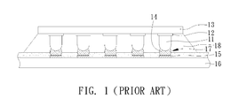
- the present invention relates to packaging substrates with conductive structure, and more particularly, to a packaging substrate with conductive structure for electrical connection to a chip.
- a semiconductor chip is electrically connected to a packaging substrate, wherein electrode pads are provided on the active face (having integrated circuits thereon) of the semiconductor chip, and conductive pads corresponding in position to the electrode pads are provided on the packaging substrate.
- Soldering structures or other conductive adhesive materials formed between the electrode pads of the semiconductor chip and the conductive pads of the packaging substrate serve as electrical and mechanical connections between the packaging substrate and the semiconductor chip.
- the flip-chip technology involves forming a plurality of metal bumps 11 on electrode pads 12 of a semiconductor chip 13 ; forming a pre-soldering structure 14 consisting of a plurality of solders on the conductive pads 15 of a packaging substrate 16 ; reflowing the pre-soldering structure 14 to the corresponding metal bumps 11 at appropriate reflow temperature to form solder joints 17 ; and applying an underfill material 18 for coupling the semiconductor chip 13 and the packaging substrate 16 to ensure integrity and reliability of the electrical connection between the semiconductor chip 13 and the packaging substrate 16 .
- FIGS. 2A to 2F a conventional method for fabricating an electrical connection structure of a packaging substrate is illustrated.
- the method comprises providing a substrate body 20 having a plurality of conductive pads 21 on a surface thereof. In this example, only one conductive pad 21 is shown for simplicity, as shown in FIG. 2A .
- a solder resist layer 22 is formed on the substrate body 20 and the conductive pad 21 .
- An opening 221 is formed in the solder resist layer 22 for exposing the surface of the conductive pad. 21
- a stencil 23 covering the substrate body 20 is provided. The stencil 23 has an opening 231 corresponding in position to the conductive pad 21 .
- a stencil printing process is performed to form a soldering material 24 in the opening 231 and the opening 221 .
- the stencil 23 is removed.
- the soldering material 24 is reflowed to form a soldering bump 24 ′, thereby providing electrical connections with the semiconductor chip in a flip-chip manner.
- joints may experience stress caused by the difference in Coefficient of Thermal Expansion (CTE) between the chip and the substrate due to temperature variation during a thermal cycle process of fabrication or when used by users after completion of packaging.
- CTE Coefficient of Thermal Expansion
- an objective of the present invention is to provide a packaging substrate with conductive structure, for releasing thermal stresses and providing good electrical connection structure, thereby preventing the joints used for electrically connecting semiconductor chips from disengaging or cracking during thermal cycles or end use, thus increasing reliability of electrical connection.
- the present invention provides a packaging substrate with conductive structure, comprising: a substrate body having at least one conductive pad on a surface thereof; a stress buffer metal layer disposed on the conductive pad, a thickness of the stress buffer metal layer being 1-20 ⁇ m; a solder resist layer disposed on the substrate body and having at least one opening therein corresponding in position to the stress buffer metal layer, with the size of the opening smaller than that of the stress buffer metal layer; a metal post disposed on a central portion of the surface of the stress buffer metal layer; and a solder bump covering the surfaces of the metal post.
- the metal post protrudes from the solder resist layer.
- a top face of the metal post may be exposed from the solder bump.
- the metal post fills the opening of the solder resist layer and is in full contact with the inner wall of the opening.
- the side surface of the metal post does not contact the inner wall of the opening, and either the opening is filled with the solder bump in full contact with the inner wall of the opening, or the solder bump does not contact the inner wall of the opening.
- the present invention further provides a packaging substrate with conductive structure, comprising: a substrate body having at least one conductive pad on a surface thereof; a stress buffer metal layer disposed on the conductive pad, a thickness of the stress buffer metal layer being 1-20 ⁇ m; a solder resist layer disposed on the substrate body and having at least one opening therein corresponding in position to the stress buffer metal layer, with the size of the opening bigger than that of the stress buffer metal layer; a metal post disposed on a central portion of the surface of the stress buffer metal layer; and a solder bump covering the surfaces of the metal post.
- the metal post protrudes from the solder resist layer.
- a top face of the metal post may be exposed from the solder bump.
- a side face of the metal post does not contact the inner wall of the opening of the solder resist layer.
- the stress buffer metal layer is made of one selected from the group consisting of tin (Sn), lead (Pb), copper (Cu), silver (Ag), bismuth (Bi), zinc (Zn), indium (In), and an alloy of a combination of the above-mentioned.
- the metal post is made of one of copper (Cu), nickel/gold (Ni/Au), and chromium (Cr), copper (Cu) plus nickel/palladium/gold (Ni/Pd/Au) surface treatment, copper (Cu) plus gold (Au) surface treatment, and copper (Cu) plus nickel/gold (Ni/Au) surface treatment.
- the various embodiments above may further include a first conductive seed-layer disposed between the substrate body and the conductive pad, and a second conductive seed-layer disposed between the metal post and the solder bump.
- the melting point of the stress buffer metal layer is slightly lower than that of the solder bump.
- a packaging substrate with conductive structure releases thermal stresses during reflow processes by the stress buffer metal layer disposed between the metal post and the conductive pad.
- the solder bump and the metal post are provided to increase the height of the conductive structure, thereby reducing the possibility of joint cracks or disengagement during thermal cycles or end use.
- FIG. 1 is a cross-sectional view of a conventional flip-chip structure
- FIGS. 2A to 2F are cross-sectional views illustrating a method for fabricating an electrical connection structure on a packaging substrate according to the prior art
- FIGS. 3A to 3N are cross-sectional views depicting a schematic flow chart of a method of fabrication according to a first embodiment of the present invention
- FIGS. 4A to 4E are cross-sectional views depicting a schematic flow chart of a method of fabrication according to a second embodiment of the present invention.
- FIG. 4 E′ is a cross-sectional view of an alternative embodiment of FIG. 4E ;
- FIGS. 5A to 5D are cross-sectional views depicting a schematic flow chart of a method of fabrication according to a third embodiment of the present invention.
- FIG. 5 D′ is a cross-sectional view of an alternative embodiment of FIG. 5D ;
- FIGS. 6A to 6E are cross-sectional views depicting a schematic flow chart of a method of fabrication according to a fourth embodiment of the present invention.
- FIG. 6 E′ is a cross-sectional view of an alternative embodiment of FIG. 6E .
- FIGS. 3A to 3N cross-sectional views depicting a first embodiment of the present inventions are shown.
- a substrate body 30 with a first conductive seed-layer 31 a formed thereon is provided.
- a patterned resist layer 32 a is formed on the surface of the first conductive seed-layer 31 a and has a plurality of open areas 320 a and 320 a ′ to expose parts of the first conductive seed-layer 31 a.
- a circuit layer 33 is formed by electroplating by the first conductive seed-layer 31 a within the open areas 320 a and 320 a ′.
- the circuit layer 33 comprises a plurality of traces and conductive pads. For simplicity and exemplary purposes, only one trace 331 and one conductive pad 332 are shown in FIG. 3B .
- a first resist layer 32 b is formed on the patterned resist layer 32 a .
- a first opening 320 b corresponding in position to the opening 320 a is formed in the first resist layer 32 b to expose the conductive pad 332 in the open area 320 a.
- a stress buffer metal layer 34 is formed by electroplating on the surface of the conductive pad 332 within the open area 320 a .
- the stress buffer metal layer 34 is made of one selected from the group consisting of tin (Sn), lead (Pb), copper (Cu), silver (Ag), bismuth (Bi), zinc (Zn), indium (In), and an alloy of a combination of the above-mentioned.
- a thickness of the stress buffer metal layer 34 is 1-20 ⁇ m.
- the first resist layer 32 b is removed, and a second resist layer 32 c is formed on the patterned resist layer 32 a .
- a second opening 320 c smaller than the first opening 320 b is formed in the second resist layer 32 c to expose a portion of top surface of the stress buffer metal layer 34 .
- a metal post 35 is formed by electroplating on the surface of the stress buffer metal layer 34 exposed from the second opening 320 c .
- the metal post 35 is made of one of copper (Cu), nickel/gold (Ni/Au), and chromium (Cr), copper (Cu) plus nickel/palladium/gold (Ni/Pd/Au) surface treatment, copper (Cu) plus gold (Au) surface treatment, and copper (Cu) plus nickel/gold (Ni/Au) surface treatment.
- the second resist layer 32 c , the patterned resist layer 32 a and the first conductive seed-layer 31 a thereunder are removed to expose the trace 331 , the conductive pad 332 , the stress buffer metal layer 34 , and the metal post 35 .
- a solder resist layer 36 is formed on the surfaces of the substrate body 30 , the trace 331 , the conductive pad 332 , the stress buffer metal layer 34 , and the metal post 35 .
- the solder resist layer 36 is thinned down to a decreased thickness so as to expose a top face and a partial side face of the metal post 35 .
- a second conductive seed-layer 31 b is formed on the surface of the solder resist layer 36 and the exposed surface of the metal post 35 .
- a third resist layer 32 d is formed on the second conductive seed-layer 31 b .
- a third opening 320 d corresponding in position to the metal post 35 is formed in the third resist layer 32 d to expose a part of the second conductive seed-layer 31 b on the metal post 35 and the solder resist layer 36 .
- a solder material 37 is formed, by electroplating, in the third opening 320 d via the second conductive seed-layer 31 b.
- the third resist layer 32 d and the second conductive seed-layer 31 b thereunder are removed so that the solder material 37 covers the exposed side face and the top face of the metal post 35 .
- solder material 37 is reflowed to form a solder bump 37 ′ for electrical connection with other electronic devices, such as semiconductor chips.
- the melting point of the stress buffer metal layer 34 is slightly lower than that of the solder bump 37 ′.
- the present invention further provides a packaging substrate with conductive structure, comprising: a substrate body 30 having at least one conductive pad 332 on a surface thereof; a stress buffer metal layer 34 disposed on the conductive pad 332 ; a solder resist layer 36 disposed on the substrate body 30 and having at least one opening 360 therein corresponding in position to the stress buffer metal layer 34 , with the size of the opening 360 smaller than that of the stress buffer metal layer 34 ; a metal post 35 disposed on a central portion of the surface of the stress buffer metal layer 34 , wherein the metal post 35 protrudes from the solder resist layer 36 , fills the opening 360 in the solder resist layer 36 , and is in full contact with the inner wall of the opening 360 ; and a solder bump 37 ′ covering the surfaces of the metal post 35 .
- the stress buffer metal layer 34 disposed between the metal post 35 and the conductive pad 332 softens and releases thermal stresses.
- the solder bump 37 ′ and the metal post 35 are provided to increase the height of the conductive structure, thereby reducing the possibility of joint cracks or disengagement.
- FIGS. 4A to 4E cross-sectional views depicting a second embodiment of the present invention are shown.
- the second embodiment is different from the first embodiment in that the solder resist layer is formed with an opening bigger than the stress buffer metal layer in size.
- An opening 360 is formed in the solder resist layer 36 to expose a portion of the top surface of the stress buffer metal layer 34 and the surfaces of the metal post 35 .
- a second conductive seed-layer 31 b is formed on the solder resist layer 36 , a portion of the top surface of the stress buffer metal layer 34 , and the surface of the metal post 35 .
- a third resist layer 32 d is formed on the second conductive seed-layer 31 b and having a third opening 320 d formed therein to expose a part of the second conductive seed-layer 31 b on the metal post 35 and the stress buffer metal layer 34 .
- a solder material 37 is formed, by electroplating, in the third opening 320 d via the second conductive seed-layer 31 b.
- the third resist layer 32 d and the second conductive seed-layer 31 b thereunder are removed so that the solder material 37 covers the side face and the top face of the metal post 35 .
- solder material 37 is reflowed to form a solder bump 37 ′ for electrical connection with other electronic devices, such as semiconductor chips.
- the third resist layer 32 d can also be formed on the top face of the metal post 35 (not shown), so that the solder bump 37 is not formed on the top face of the metal post 35 . After reflowing, the solder bump 37 ′ does not cover the top face of the metal post 35 , and the metal post 35 is exposed from the solder bump 37 ′.
- the present invention further provides a packaging substrate with conductive structure, comprising: a substrate body 30 having at least one conductive pad 332 on a surface thereof; a stress buffer metal layer 34 disposed on the conductive pad 332 ; a solder resist layer 36 disposed on the substrate body 30 and having at least one opening 360 therein corresponding in position to the stress buffer metal layer 34 , with the size of the opening 360 smaller than that of the stress buffer metal layer 34 ; a metal post 35 disposed on a central portion of the surface of the stress buffer metal layer 34 , wherein the metal post 35 protrudes from the solder resist layer 36 , and the side face of the metal post 35 does not contact the inner wall of the opening 360 in the solder resist layer 36 ; and a solder bump 37 ′ covering the surfaces of the exposed metal posts 35 , as shown in FIG. 4E .
- the top face of the metal post 35 may be exposed from the solder bump 37 ′, as shown in FIG. 4 E′.
- FIGS. 5A to 5D cross-sectional views depicting a third embodiment of the present invention are shown.
- the third embodiment is different from the previous embodiment in that the solder bump not only covers the metal post but also completely fills the opening in the solder resist layer.
- the method of fabrication is similar to the second embodiment, and it will not be further discussed.
- the present invention further provides a packaging substrate with conductive structure, comprising: a substrate body 30 having at least one conductive pads 332 on a surface thereof; a stress buffer metal layer 34 disposed on the conductive pad 332 , a thickness of the stress buffer metal layer 34 being 1-20 ⁇ m; a solder resist layer 36 disposed on the substrate body 30 and having at least one opening 360 therein corresponding in position to the stress buffer metal layer 34 , with the size of the opening 360 smaller than that of the stress buffer metal layer 34 ; a metal post 35 disposed on a central portion of the surface of the stress buffer metal layer 34 , wherein the metal post 35 protrudes from the solder resist layer 36 , and the side face of the metal post 35 does not contact the inner wall of the opening 360 in the solder resist layer 36 ; and a solder bump 37 ′ covering the metal post 35 and filling the opening 360 in the solder resist layer 36 , such that the solder bump 37 ′ is in full contact with the inner wall of the opening 360 , as shown in FIG.
- FIGS. 6A to 6E cross-sectional views depicting a fourth embodiment of the present invention are shown.
- the fourth embodiment is different from the previous embodiment in that the opening in the solder resist layer is bigger than the stress buffer metal layer 34 in size.
- the method of fabrication is similar to the second embodiment, and it will not be further discussed.
- the present invention further provides a packaging substrate with conductive structure, comprising: a substrate body 30 having at least one conductive pad 332 on a surface thereof; a stress buffer metal layer 34 disposed on the conductive pad 332 , a thickness of the stress buffer metal layer 34 being 1-20 ⁇ m; a solder resist layer 36 disposed on the substrate body 30 and having at least one opening 360 therein corresponding in position to the stress buffer metal layer 34 , with the size of the opening 360 bigger than that of the stress buffer metal layer 34 ; a metal post 35 disposed on a central portion of the surface of the stress buffer metal layer 34 and protruding from the solder resist layer 36 ; and a solder bump 37 ′ covering the surfaces of the metal post 35 , as shown in FIG. 6E .
- a top face of the metal post 35 may be exposed from the solder bump 37 ′, as shown in FIG. 6 E′.
- a packaging substrate with conductive structure utilizes the stress buffer metal layer formed between the conductive pad and the metal post to release thermal stresses, and utilizes the metal post and the solder bump to increase the height of the conductive structure, thereby providing a good electrical connection structure and preventing disengagement or cracking of joints electrically connected to semiconductor chips during thermal cycles or end use.
Landscapes
- Engineering & Computer Science (AREA)
- Manufacturing & Machinery (AREA)
- Microelectronics & Electronic Packaging (AREA)
- Wire Bonding (AREA)
Abstract
Description
Claims (17)
Priority Applications (1)
| Application Number | Priority Date | Filing Date | Title |
|---|---|---|---|
| US13/355,311 US8779300B2 (en) | 2007-07-19 | 2012-01-20 | Packaging substrate with conductive structure |
Applications Claiming Priority (5)
| Application Number | Priority Date | Filing Date | Title |
|---|---|---|---|
| TW096126297 | 2007-07-19 | ||
| TW96126297A | 2007-07-19 | ||
| TW096126297A TWI378544B (en) | 2007-07-19 | 2007-07-19 | Package substrate with electrically connecting structure |
| US12/175,348 US8101866B2 (en) | 2007-07-19 | 2008-07-17 | Packaging substrate with conductive structure |
| US13/355,311 US8779300B2 (en) | 2007-07-19 | 2012-01-20 | Packaging substrate with conductive structure |
Related Parent Applications (1)
| Application Number | Title | Priority Date | Filing Date |
|---|---|---|---|
| US12/175,348 Continuation-In-Part US8101866B2 (en) | 2007-07-19 | 2008-07-17 | Packaging substrate with conductive structure |
Publications (2)
| Publication Number | Publication Date |
|---|---|
| US20120181688A1 US20120181688A1 (en) | 2012-07-19 |
| US8779300B2 true US8779300B2 (en) | 2014-07-15 |
Family
ID=46490168
Family Applications (1)
| Application Number | Title | Priority Date | Filing Date |
|---|---|---|---|
| US13/355,311 Active 2029-04-16 US8779300B2 (en) | 2007-07-19 | 2012-01-20 | Packaging substrate with conductive structure |
Country Status (1)
| Country | Link |
|---|---|
| US (1) | US8779300B2 (en) |
Families Citing this family (9)
| Publication number | Priority date | Publication date | Assignee | Title |
|---|---|---|---|---|
| JP5782823B2 (en) * | 2011-04-27 | 2015-09-24 | 日亜化学工業株式会社 | Nitride semiconductor light emitting device and manufacturing method thereof |
| US9484291B1 (en) * | 2013-05-28 | 2016-11-01 | Amkor Technology Inc. | Robust pillar structure for semicondcutor device contacts |
| TWI514530B (en) * | 2013-08-28 | 2015-12-21 | 威盛電子股份有限公司 | Circuit substrate, semiconductor package structure and circuit substrate process |
| TWI474417B (en) * | 2014-06-16 | 2015-02-21 | 恆勁科技股份有限公司 | Packaging method |
| JP2016012702A (en) * | 2014-06-30 | 2016-01-21 | ファナック株式会社 | Print circuit board balancing wettability and anticorrosion of solder coat and manufacturing method of the same |
| TWI533771B (en) * | 2014-07-17 | 2016-05-11 | 矽品精密工業股份有限公司 | Coreless package substrate and its preparation method |
| US11495516B2 (en) * | 2020-11-20 | 2022-11-08 | Nanya Technology Corporation | Semiconductor device with thermal release layer and method for fabricating the same |
| KR20220109642A (en) * | 2021-01-29 | 2022-08-05 | 엘지이노텍 주식회사 | Circuit board and package substrate including the same |
| CN113540004B (en) * | 2021-08-18 | 2025-06-24 | 甬矽电子(宁波)股份有限公司 | Bump package structure and method for preparing bump package structure |
Citations (32)
| Publication number | Priority date | Publication date | Assignee | Title |
|---|---|---|---|---|
| US4818728A (en) * | 1986-12-03 | 1989-04-04 | Sharp Kabushiki Kaisha | Method of making a hybrid semiconductor device |
| US5317801A (en) * | 1990-04-23 | 1994-06-07 | Nippon Mektron, Ltd. | Method of manufacture of multilayer circuit board |
| US5872404A (en) * | 1994-06-02 | 1999-02-16 | Lsi Logic Corporation | Interconnect bump for flip-chip integrated circuit including integral standoff and hourglass shaped solder coating |
| US6077765A (en) * | 1996-10-16 | 2000-06-20 | Casio Computer Co., Ltd. | Structure of bump electrode and method of forming the same |
| US6281106B1 (en) * | 1999-11-25 | 2001-08-28 | Delphi Technologies, Inc. | Method of solder bumping a circuit component |
| US20010040290A1 (en) * | 2000-05-01 | 2001-11-15 | Seiko Epson Corporation | Method for forming bump, semiconductor device and method for making the same, circuit board, and electronic device |
| US6372622B1 (en) * | 1999-10-26 | 2002-04-16 | Motorola, Inc. | Fine pitch bumping with improved device standoff and bump volume |
| US6426281B1 (en) * | 2001-01-16 | 2002-07-30 | Taiwan Semiconductor Manufacturing Company | Method to form bump in bumping technology |
| US6555296B2 (en) * | 2001-04-04 | 2003-04-29 | Siliconware Precision Industries Co., Ltd. | Fine pitch wafer bumping process |
| US6559540B2 (en) * | 2000-02-09 | 2003-05-06 | Nec Electronics Corporation | Flip-chip semiconductor device and method of forming the same |
| US6613663B2 (en) * | 2000-12-08 | 2003-09-02 | Nec Electronics Corporation | Method for forming barrier layers for solder bumps |
| US20030214795A1 (en) * | 2002-05-17 | 2003-11-20 | Fujitsu Limited | Electronic component with bump electrodes, and manufacturing method thereof |
| US20040021234A1 (en) * | 2002-07-15 | 2004-02-05 | Kazutaka Shibata | Semiconductor device and manufacturing method thereof |
| US6780751B2 (en) * | 2002-10-09 | 2004-08-24 | Freescale Semiconductor, Inc. | Method for eliminating voiding in plated solder |
| US6818545B2 (en) * | 2001-03-05 | 2004-11-16 | Megic Corporation | Low fabrication cost, fine pitch and high reliability solder bump |
| US20040232562A1 (en) * | 2003-05-23 | 2004-11-25 | Texas Instruments Incorporated | System and method for increasing bump pad height |
| US6849534B2 (en) * | 2002-10-25 | 2005-02-01 | Via Technologies, Inc. | Process of forming bonding columns |
| US6917106B2 (en) * | 2002-10-24 | 2005-07-12 | Intel Corporation | Selective ball-limiting metallurgy etching processes for fabrication of electroplated tin bumps |
| US6945084B2 (en) * | 2000-03-28 | 2005-09-20 | Kocks Technik Gmbh & Co. Kg | Rolling mill for rolling or sizing metal pipes |
| US6956292B2 (en) * | 2001-09-10 | 2005-10-18 | Taiwan Semiconductor Manufacturing Co., Ltd. | Bumping process to increase bump height and to create a more robust bump structure |
| US7008867B2 (en) * | 2003-02-21 | 2006-03-07 | Aptos Corporation | Method for forming copper bump antioxidation surface |
| US20060094224A1 (en) * | 2004-11-03 | 2006-05-04 | Advanced Semiconductor Engineering, Inc. | Bumping process and structure thereof |
| US7135770B2 (en) * | 2002-02-07 | 2006-11-14 | Nec Corporation | Semiconductor element with conductive columnar projection and a semiconductor device with conductive columnar projection |
| US7202421B2 (en) * | 2003-01-30 | 2007-04-10 | Seiko Epson Corporation | Electronic elements, method for manufacturing electronic elements, circuit substrates, method for manufacturing circuit substrates, electronic devices and method for manufacturing electronic devices |
| US7227262B2 (en) * | 2003-10-03 | 2007-06-05 | Rohm Co., Ltd. | Manufacturing method for semiconductor device and semiconductor device |
| US7235428B2 (en) * | 2002-11-21 | 2007-06-26 | Rohm Co., Ltd. | Semiconductor device production method |
| US7250362B2 (en) * | 2003-09-09 | 2007-07-31 | Advanced Semiconductor Engineering Inc. | Solder bump structure and method for forming the same |
| US20070281389A1 (en) * | 2006-06-01 | 2007-12-06 | Phoenix Precision Technology Corporation | Method for fabricating electrical conductive structure of circuit board |
| US20070281557A1 (en) * | 2006-06-06 | 2007-12-06 | Phoenix Precision Technology Corporation | Method of fabricating circuit board having different electrical connection structures |
| US7341949B2 (en) * | 2003-08-21 | 2008-03-11 | Siliconware Precision Industries Co., Ltd. | Process for forming lead-free bump on electronic component |
| US7358174B2 (en) * | 2004-04-13 | 2008-04-15 | Amkor Technology, Inc. | Methods of forming solder bumps on exposed metal pads |
| US7382049B2 (en) * | 2005-08-30 | 2008-06-03 | Via Technologies, Inc. | Chip package and bump connecting structure thereof |
-
2012
- 2012-01-20 US US13/355,311 patent/US8779300B2/en active Active
Patent Citations (36)
| Publication number | Priority date | Publication date | Assignee | Title |
|---|---|---|---|---|
| US4818728A (en) * | 1986-12-03 | 1989-04-04 | Sharp Kabushiki Kaisha | Method of making a hybrid semiconductor device |
| US5317801A (en) * | 1990-04-23 | 1994-06-07 | Nippon Mektron, Ltd. | Method of manufacture of multilayer circuit board |
| US5872404A (en) * | 1994-06-02 | 1999-02-16 | Lsi Logic Corporation | Interconnect bump for flip-chip integrated circuit including integral standoff and hourglass shaped solder coating |
| US6077765A (en) * | 1996-10-16 | 2000-06-20 | Casio Computer Co., Ltd. | Structure of bump electrode and method of forming the same |
| US6372622B1 (en) * | 1999-10-26 | 2002-04-16 | Motorola, Inc. | Fine pitch bumping with improved device standoff and bump volume |
| US6281106B1 (en) * | 1999-11-25 | 2001-08-28 | Delphi Technologies, Inc. | Method of solder bumping a circuit component |
| US6559540B2 (en) * | 2000-02-09 | 2003-05-06 | Nec Electronics Corporation | Flip-chip semiconductor device and method of forming the same |
| US6945084B2 (en) * | 2000-03-28 | 2005-09-20 | Kocks Technik Gmbh & Co. Kg | Rolling mill for rolling or sizing metal pipes |
| US20010040290A1 (en) * | 2000-05-01 | 2001-11-15 | Seiko Epson Corporation | Method for forming bump, semiconductor device and method for making the same, circuit board, and electronic device |
| US6613663B2 (en) * | 2000-12-08 | 2003-09-02 | Nec Electronics Corporation | Method for forming barrier layers for solder bumps |
| US6426281B1 (en) * | 2001-01-16 | 2002-07-30 | Taiwan Semiconductor Manufacturing Company | Method to form bump in bumping technology |
| US6818545B2 (en) * | 2001-03-05 | 2004-11-16 | Megic Corporation | Low fabrication cost, fine pitch and high reliability solder bump |
| US6555296B2 (en) * | 2001-04-04 | 2003-04-29 | Siliconware Precision Industries Co., Ltd. | Fine pitch wafer bumping process |
| US6956292B2 (en) * | 2001-09-10 | 2005-10-18 | Taiwan Semiconductor Manufacturing Co., Ltd. | Bumping process to increase bump height and to create a more robust bump structure |
| US7449406B2 (en) * | 2002-02-07 | 2008-11-11 | Nec Corporation | Semiconductor element and a producing method for the same, and a semiconductor device and a producing method for the same |
| US7135770B2 (en) * | 2002-02-07 | 2006-11-14 | Nec Corporation | Semiconductor element with conductive columnar projection and a semiconductor device with conductive columnar projection |
| US20030214795A1 (en) * | 2002-05-17 | 2003-11-20 | Fujitsu Limited | Electronic component with bump electrodes, and manufacturing method thereof |
| US20040021234A1 (en) * | 2002-07-15 | 2004-02-05 | Kazutaka Shibata | Semiconductor device and manufacturing method thereof |
| US6780751B2 (en) * | 2002-10-09 | 2004-08-24 | Freescale Semiconductor, Inc. | Method for eliminating voiding in plated solder |
| US6917106B2 (en) * | 2002-10-24 | 2005-07-12 | Intel Corporation | Selective ball-limiting metallurgy etching processes for fabrication of electroplated tin bumps |
| US6902997B2 (en) * | 2002-10-25 | 2005-06-07 | Via Technologies, Inc. | Process of forming bonding columns |
| US6849534B2 (en) * | 2002-10-25 | 2005-02-01 | Via Technologies, Inc. | Process of forming bonding columns |
| US7235428B2 (en) * | 2002-11-21 | 2007-06-26 | Rohm Co., Ltd. | Semiconductor device production method |
| US7202421B2 (en) * | 2003-01-30 | 2007-04-10 | Seiko Epson Corporation | Electronic elements, method for manufacturing electronic elements, circuit substrates, method for manufacturing circuit substrates, electronic devices and method for manufacturing electronic devices |
| US7008867B2 (en) * | 2003-02-21 | 2006-03-07 | Aptos Corporation | Method for forming copper bump antioxidation surface |
| US20040232562A1 (en) * | 2003-05-23 | 2004-11-25 | Texas Instruments Incorporated | System and method for increasing bump pad height |
| US7341949B2 (en) * | 2003-08-21 | 2008-03-11 | Siliconware Precision Industries Co., Ltd. | Process for forming lead-free bump on electronic component |
| US7250362B2 (en) * | 2003-09-09 | 2007-07-31 | Advanced Semiconductor Engineering Inc. | Solder bump structure and method for forming the same |
| US7227262B2 (en) * | 2003-10-03 | 2007-06-05 | Rohm Co., Ltd. | Manufacturing method for semiconductor device and semiconductor device |
| US7638421B2 (en) * | 2003-10-03 | 2009-12-29 | Rohm Co., Ltd. | Manufacturing method for semiconductor device and semiconductor device |
| US7358174B2 (en) * | 2004-04-13 | 2008-04-15 | Amkor Technology, Inc. | Methods of forming solder bumps on exposed metal pads |
| US20060094224A1 (en) * | 2004-11-03 | 2006-05-04 | Advanced Semiconductor Engineering, Inc. | Bumping process and structure thereof |
| US7382049B2 (en) * | 2005-08-30 | 2008-06-03 | Via Technologies, Inc. | Chip package and bump connecting structure thereof |
| US20070281389A1 (en) * | 2006-06-01 | 2007-12-06 | Phoenix Precision Technology Corporation | Method for fabricating electrical conductive structure of circuit board |
| US7419897B2 (en) * | 2006-06-06 | 2008-09-02 | Phoenix Precision Technology Corporation | Method of fabricating circuit board having different electrical connection structures |
| US20070281557A1 (en) * | 2006-06-06 | 2007-12-06 | Phoenix Precision Technology Corporation | Method of fabricating circuit board having different electrical connection structures |
Also Published As
| Publication number | Publication date |
|---|---|
| US20120181688A1 (en) | 2012-07-19 |
Similar Documents
| Publication | Publication Date | Title |
|---|---|---|
| US8101866B2 (en) | Packaging substrate with conductive structure | |
| US8779300B2 (en) | Packaging substrate with conductive structure | |
| US8101514B2 (en) | Semiconductor device having elastic solder bump to prevent disconnection | |
| TWI245402B (en) | Rod soldering structure and manufacturing process thereof | |
| US8884448B2 (en) | Flip chip interconnection with double post | |
| US8164003B2 (en) | Circuit board surface structure and fabrication method thereof | |
| CN101007365A (en) | Joining method, method of mounting semiconductor package, and substrate-joining structure | |
| EP2020835B1 (en) | A circuit board | |
| JP4993754B2 (en) | PGA type wiring board and manufacturing method thereof | |
| JPH10135613A (en) | Wiring board | |
| JP2006302929A (en) | PROJECT ELECTRODE FOR CONNECTING ELECTRONIC COMPONENT, ELECTRONIC COMPONENT MOUNTING BODY USING SAME, AND METHOD FOR PRODUCING THEM | |
| TWI242866B (en) | Process of forming lead-free bumps on electronic component | |
| JP3836349B2 (en) | Semiconductor device and manufacturing method thereof | |
| TWI336516B (en) | Surface structure of package substrate and method for manufacturing the same | |
| KR100723497B1 (en) | Printed circuit board having two or more surface treatments on solder ball lands and semiconductor package including the same | |
| TW589727B (en) | Bumping structure and fabrication process thereof | |
| JP3838530B2 (en) | Manufacturing method of semiconductor device | |
| US7901997B2 (en) | Method of manufacturing semiconductor device | |
| JP4940662B2 (en) | Solder bump, method of forming solder bump, and semiconductor device | |
| KR100761863B1 (en) | Printed circuit board having two or more surface treatments on solder ball lands and semiconductor package including the same | |
| JPH10261737A (en) | Wiring board | |
| JPH05136216A (en) | Semiconductor mounting device | |
| KR100716869B1 (en) | Conductive bump structure of semiconductor chip and forming method | |
| TWI473181B (en) | Package substrate with electrical connection structure and preparation method thereof | |
| JP2003258156A (en) | Wiring board |
Legal Events
| Date | Code | Title | Description |
|---|---|---|---|
| STCF | Information on status: patent grant |
Free format text: PATENTED CASE |
|
| MAFP | Maintenance fee payment |
Free format text: PAYMENT OF MAINTENANCE FEE, 4TH YEAR, LARGE ENTITY (ORIGINAL EVENT CODE: M1551) Year of fee payment: 4 |
|
| MAFP | Maintenance fee payment |
Free format text: PAYMENT OF MAINTENANCE FEE, 8TH YEAR, LARGE ENTITY (ORIGINAL EVENT CODE: M1552); ENTITY STATUS OF PATENT OWNER: LARGE ENTITY Year of fee payment: 8 |
|
| MAFP | Maintenance fee payment |
Free format text: PAYMENT OF MAINTENANCE FEE, 12TH YEAR, LARGE ENTITY (ORIGINAL EVENT CODE: M1553); ENTITY STATUS OF PATENT OWNER: LARGE ENTITY Year of fee payment: 12 |