US8723372B2 - System for inducing a high efficiency conductive state in materials - Google Patents
System for inducing a high efficiency conductive state in materials Download PDFInfo
- Publication number
- US8723372B2 US8723372B2 US13/192,060 US201113192060A US8723372B2 US 8723372 B2 US8723372 B2 US 8723372B2 US 201113192060 A US201113192060 A US 201113192060A US 8723372 B2 US8723372 B2 US 8723372B2
- Authority
- US
- United States
- Prior art keywords
- signal
- mass
- response
- target mass
- conductor
- Prior art date
- Legal status (The legal status is an assumption and is not a legal conclusion. Google has not performed a legal analysis and makes no representation as to the accuracy of the status listed.)
- Expired - Fee Related, expires
Links
Images


Classifications
-
- H—ELECTRICITY
- H01—ELECTRIC ELEMENTS
- H01M—PROCESSES OR MEANS, e.g. BATTERIES, FOR THE DIRECT CONVERSION OF CHEMICAL ENERGY INTO ELECTRICAL ENERGY
- H01M10/00—Secondary cells; Manufacture thereof
- H01M10/42—Methods or arrangements for servicing or maintenance of secondary cells or secondary half-cells
-
- H—ELECTRICITY
- H01—ELECTRIC ELEMENTS
- H01M—PROCESSES OR MEANS, e.g. BATTERIES, FOR THE DIRECT CONVERSION OF CHEMICAL ENERGY INTO ELECTRICAL ENERGY
- H01M10/00—Secondary cells; Manufacture thereof
- H01M10/06—Lead-acid accumulators
-
- Y—GENERAL TAGGING OF NEW TECHNOLOGICAL DEVELOPMENTS; GENERAL TAGGING OF CROSS-SECTIONAL TECHNOLOGIES SPANNING OVER SEVERAL SECTIONS OF THE IPC; TECHNICAL SUBJECTS COVERED BY FORMER USPC CROSS-REFERENCE ART COLLECTIONS [XRACs] AND DIGESTS
- Y02—TECHNOLOGIES OR APPLICATIONS FOR MITIGATION OR ADAPTATION AGAINST CLIMATE CHANGE
- Y02E—REDUCTION OF GREENHOUSE GAS [GHG] EMISSIONS, RELATED TO ENERGY GENERATION, TRANSMISSION OR DISTRIBUTION
- Y02E60/00—Enabling technologies; Technologies with a potential or indirect contribution to GHG emissions mitigation
- Y02E60/10—Energy storage using batteries
Definitions
- This invention relates generally to a method of inducing and maintaining a high efficiency conductive state in a conductive mass, and more particularly, maintaining a high efficiency conductive state in common conductive metals, including semi-conductive elements, above or below room temperature.
- High-temperature superconducting materials such as Bi—Sr—Ca—Cu—O, found in U.S. Pat. No. 5,665,662, transition to a superconducting state at temperatures near 90K to 105K.
- This transition temperature, or Tc requires coolant to keep the material below the transition temperature (Tc) to maintain the desired conductive state.
- the manufacture of these higher transition (Tc) temperature superconductors are complex—such as bismuth-strontium-calcium-copper oxide, or yttrium-barium-copper oxide, and include a careful sintering process in maintaining a specific desired chemical composition.
- the resulting material is also limited in ductility, compared to common metals, as there are parametric limits to the brittleness of the final chemical composition.
- the present invention involves a method of injecting a precisely tuned signal into a common conductive metal, such as aluminum, to create an exited ionic state within the entire mass, resulting in the mass exhibiting similar characteristics of a sustained homogeneous charge density wave (CDW).
- An electrical signal generator is used to produce the complex and precisely tuned and phase matched wave form frequencies which are applied to, and match the mass lattice tuning, of the target mass.
- Various locations of injection of the stimulation signal include a single point of injection ( FIG. 4 ) or multiple locations of injection ( FIG. 3 ) both of which depends on the symmetry or complexity of the target mass geometry.
- a non-bonded physical pressure based conductive point wire injection method may be employed.
- FIG. 5 electrostatic field induction
- FIG. 7 magnetic field induction
- FIG. 6 photonic induction
- FIG. 6 a modulated light beam
- the high efficiency conductive state has been observed to be transmittable to other metals or semiconductors by simple physical contact.
- Suitable physical contact, from the target mass to another metal or semiconductor material, has been found through bonding using a dielectric based epoxy ( 52 ) as shown in FIG. 16 , by welding ( 69 ) as shown in FIG. 20 , by conductive electrical epoxy bonding compounds ( 53 c ) as shown in FIG. 17 , or by silicon die ( 65 ) in FIG. 19 .
- FIG. 1 is an illustration of symmetrical injection points at opposite corners of a symmetrical metal conductor and target mass.
- FIG. 2 is an illustration of symmetrical injection points at the center of and opposing sides of a symmetrical metal conductor and target mass.
- FIG. 3 is an illustration of symmetrical injection points at the corners and at offset symmetrical and opposing sides of a symmetrical metal conductor and target mass.
- FIG. 4 is an illustration of a single injection point at a corner of a symmetrical metal conductor and target mass.
- FIG. 5 is an illustration of symmetrical injection points using electrostatic field stimulation at opposite corners of a symmetrical metal conductor and target mass.
- FIG. 6 is an illustration of symmetrical injection points using a LASER to stimulate at opposite corners of a symmetrical metal conductor and target mass.
- FIG. 7 is an illustration of a metal conductor and target mass stimulated by a distributed magnetic field.
- FIG. 8 is a drawing illustrating relative phase shifting of multiple subharmonic signals that are part of the desired signal parameter tuning in the modulation of the complex carrier wave to a given target mass.
- FIG. 9 is a drawing illustrating a single sine-wave modulated subharmonic on a higher frequency carrier sine wave.
- FIG. 10 is a drawing illustrating multiple subharmonic signals that are part of the desired signal modulation of the complex carrier wave to a given target mass.
- FIG. 11 is a drawing of the multiple subharmonic signals of FIG. 10 incorporated into a complex carrier wave.
- FIG. 12 is a drawing illustrating an alternate form of a complex carrier wave with subharmonic injection using a digital form of pulse width modulation (PWM) to induce the desired subharmonic signals while injecting a given target mass.
- PWM pulse width modulation
- FIG. 13 is an illustration of a lead-acid battery where the terminals of the battery are used as injection points and the target mass is the internal plates of the battery.
- FIG. 14 is an illustration of a small battery where the terminals of the battery are used as injection points and the target mass is the internal electrode(s) of the battery.
- FIG. 15 is an illustration of a target mass bonded to the substrate of a computer IC where the target mass is used to induce an excited state into the substrate and transistor layers of the IC.
- FIG. 16 is an illustration of a target mass bonded to a conductor of another type of mass whereby the target mass is used to induce an excited state into the conductor.
- FIG. 17 is an illustration of a target mass physically clamped to a conductor whereby the target mass is used to induce an excited state into the conductor.
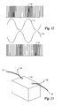
- FIG. 18 is an illustration of a series of harmonic peak frequencies shown in a Fast Fourier Transform (FFT) plot, from a Dynamic Signal Analyzer, whereby the target mass responds to in a tuned state during signal injection testing.
- FFT Fast Fourier Transform
- FIG. 19 is an illustration of a semiconductor device where the target mass is imbedded within the semiconductor silicon.
- FIG. 20 is an illustration of a target mass conductively bonded to a copper conductor trace where the target mass, when excited, will induce an excited state into the current flow within the copper trace.
- FIG. 21 is an illustration of a target mass shape formed as part of a conductor where current flow through the target mass, when the target mass shape is excited, will induce an excited state into the current flow within the conductor.
- a mass lattice excitation state in a common metal conductor may be found.
- This mass lattice excitation state is also achievable in semiconductor materials with the afore-described programmable waveform generator.
- the preferred temperatures of this excitation state is greater than ⁇ 10 degrees C., preferably greater than 0 degrees C., and more preferably greater than 25 degrees C. In this preferred excitation state, the resistance of the material is decreased, and preferably substantially decreased toward zero resistance.
- This mass lattice excitation state, of a target mass has been observed to produce special conductive states in metal conductors and in semiconductors.
- the degree of the change (lowering) in conductivity within conductors, from this induced special excitation method is proportional to the degree of the intensity of the mass lattice excitation.
- semiconductor devices have been observed to increase in switching speed while lowering their operating switching bias, lowering operating switching thresholds, lowering their operating current, lowering resistance, and lowering noise levels all in proportion to the degree of the intensity of the induced mass lattice excitation from a target mass.
- the broad phonon excitation is believed to contain a wide spectrum of phonon frequencies such that this spectrum provides a matched tuning of the appropriate phonons, facilitating absorption, into the atomic structure of the conductive and semiconductor elements—even if differing in the isotope element of the excited target mass.
- an optimal mass lattice excitation state may be determined for a metal conductor or for a semiconductor material.
- Secondary ( 5 ) and tertiary ( 6 ) subharmonics are generally found within 100 hz above or below the primary subharmonic ( 4 ).
- Finding the primary subharmonic includes an empirical tuning process where the carrier ( 56 ) develops a slow observable undulation ( 58 ), on the skirts of the FFT plot as shown in FIG. 18 .
- a harmonic series of frequencies ( 57 ) will increase in amplitude when approaching the optimal mass lattice excitation for a particular target mass.
- Further tuning of the secondary and tertiary subharmonic optimization involves adjusting the phase relationship between the primary subharmonic ( 4 ), the secondary subharmonic ( 5 ), and the tertiary subharmonic ( 6 ).
- An example phase relationship ( 56 , 57 , 58 ) of the subharmonic frequencies ( 59 , 60 , 61 ) are shown in FIG. 8 .
- the slow undulation ( 58 ) is preferably at a frequency of less than 1,000 hertz, and more preferably at a frequency of less than 500 hertz.
- the carrier FFT amplitude ( 56 ) preferably likewise has an amplitude that is substantially larger than the corresponding harmonic FFT amplitudes ( 57 ).
- the harmonic FFT amplitudes ( 57 ) are preferably 25% or less of the amplitude of the carrier FFT amplitude ( 56 ), and more preferably 10% or less of the amplitude of the carrier FFT amplitude ( 56 ).
- transient changes in the FFT amplitude(s) that occur occasionally, generally in the frequency range of the slow undulation ( 58 ), having an amplitude of preferably greater than 10% of the carrier FFT amplitude ( 56 ), and more preferably greater than 20% of the carrier FFT amplitude ( 56 ).
- the duration of the transient is preferably less than 1000 milliseconds, more preferably less than 750 milliseconds, and more preferably less than 500 milliseconds.
- Excitation injection current is generally below 500 milli-amperes and above 10 micro-amperes, with two or more physical injection wires, depending on the desired strength of the excitation state within the target mass. Since the material is typically conductive, and would typically result in a “short” between the conductors, however when reaching the appropriate state the carrier and the harmonics are created.
- a transition may occur where the carrier FFT ( 56 ) increases substantially in amplitude and the slow undulation ( 58 ) tends to substantially decrease or is otherwise no longer readily observable. Also, when the system is suitably tuned to the appropriate state, an increase in the number of harmonics ( 57 ) having generally the same amplitude will occur, such as double the number of such harmonics.
- Odd harmonic frequency relationships of the carrier to the primary subharmonic frequency have been observed to be less stable than an even harmonic ratio.
- FIG. 10 illustrates three subharmonic frequencies of a primary frequency ( 4 ), a 2 ⁇ upper harmonic to the primary subharmonic frequency ( 5 ), and a 4 ⁇ harmonic frequency to the primary subharmonic frequency ( 6 ). Modulation of these three subharmonic frequencies ( 4 , 5 , 6 ), using an upper harmonic carrier, is illustrated in FIG. 11 . The resulting modulated carrier signal ( 7 ) is injected into the target mass.
- a subharmonic base frequency ( 31 ) may be encoded into a carrier based PWM digital signal ( 30 ).
- a second shifted subharmonic signal ( 33 ), encoded on a carrier using PWM ( 32 ) allows phase shift injection.
- the illustration shows a 180 degree phase shift between one injection carrier signal ( 30 ), PWM subharmonic modulated ( 31 ), and a second injection carrier signal ( 32 ), PWM subharmonic modulated ( 33 ).
- This digital PWM method provides the ability to encode multiple subharmonic frequencies, using PWM power modulation, on a base carrier frequency.
- Mass lattice excitation in its simplest form, shown in FIG. 4 , is achieved using a single subharmonic frequency modulated carrier ( 29 ) injected into a target mass ( 1 d ) with a single injection wire ( 16 ).
- a target mass ( 1 d ) is a rectangular 6061 aluminum mass with polished smooth surfaces with dimensions of 0.125 inches square by 0.500 inches in length.
- the injection wire ( 16 ) of 0.010 inch diameter 14K gold wire is weld bonded to the target mass ( 1 d ) at the corner with the welded wire exit angle aligned to the apex of the corner tip of the target mass.
- FIG. 1 Improved performance of excitation of the target mass ( 1 ), shown in FIG. 1 , is realized with two injection wires ( 2 , 3 ) at symmetrically opposite corners of the target mass ( 1 ).
- An alternative embodiment of paired injection wires ( 8 , 9 ) is illustrated in FIG. 2 with two symmetrically located injection points at the center of opposite faces in the target mass ( 1 b ).
- a third embodiment, in FIG. 3 includes six injection wires bonded at symmetrically balanced locations on one half of the target mass ( 1 c ) using three injection wires ( 10 , 11 , 12 ) and three injection wires ( 13 , 14 , 15 ) on the other half of the target mass.
- injection locations are shifted with respect to each other, as in the case of three or six injection wires ( 10 , 11 , 12 , 13 , 14 , 15 ).
- phase shifting of the injected modulated carrier and the subharmonic frequencies are required to properly develop the mass lattice excitation.
- FIG. 8 illustrates phase shift ( 56 , 57 , 58 ) of a set of subharmonic frequencies ( 59 , 60 , 61 ). Additional injection locations, such as illustrated, provides a method of increasing the Q of the mass lattice excitation effect to compensate for materials whereby the element isotope purity of the target mass is generally less than 90% pure.
- FIG. 7 Another method of mass lattice excitation, shown in FIG. 7 , is employed using target mass materials having magnetic permeability properties, whereby the magnetic flux ( 27 ) is stimulated using a subharmonic modulated carrier frequency.
- the magnetic flux acts as the injection source to the target mass ( 1 g ).
- the injection method uses a wide surface area of the target mass. In this application, the target mass material is not a magnet. Similarly, a wide surface area injection of the target mass may be accomplished as shown in FIG. 7 with a higher carrier frequency in the RF spectrum to achieve electromagnetic coupling.
- Injection of the target mass may be alternately accomplished using electrostatic fields through plates ( 18 , 21 ) as shown in FIG. 5 .
- the electrostatic fields ( 19 , 20 ) develop near the corner points of the target mass ( 1 e ) forming injection points.
- This method has the advantage of creating a loosely coupled method of stimulation as the injection wires ( 17 , 22 ) are not directly bonded to the mass. This method provides another advantage of electrical isolation from the target mass material.
- FIG. 6 illustrates another method of isolated stimulation of a target mass ( 1 f ) using a focused modulated light beam ( 24 , 25 ) with photon based light sources ( 23 , 26 ) such as a LASER using a tuned carrier modulated signal.
- FIG. 13 illustrates a method of injecting a tuned carrier modulated signal, through the terminals of a battery, through stimulation wires ( 35 , 36 ), whereby the internal plates of the battery ( 34 ) are used as the target mass to be brought into a high efficiency conductive state.
- FIG. 14 alternately illustrates a method of injecting a tuned carrier modulated signal, through the terminals of a small battery ( 43 ), through stimulation wires ( 39 , 40 ), whereby the internal metal plate of the battery is used as the target mass to be brought into a high efficiency conductive state.
- FIG. 16 illustrates a method of exciting a conductor ( 51 ) into a high efficiency conductive state using a target mass ( 1 k ), that is bonded by either a conductive or insulator based bonding material ( 52 )—such as an epoxy—, and injecting a tuned carrier modulated signal through injection wires ( 49 , 50 ).
- FIG. 17 illustrates an alternate method of exciting a conductor ( 53 e ) into a efficiency conductive state using a target mass ( 53 ) and injection wires ( 53 a , 53 b ), that is physically clamped ( 53 d ) to the conductor ( 53 e ).
- the target mass ( 53 ) transfers its excitation state through the physical contact of the seam of the clamp blade ( 53 c ), which is bonded to the target mass by either a conductive or insulator based bonding material.
- FIG. 15 illustrates a method of exciting a computer IC die ( 45 ) into a high efficiency conductive and semiconductor operating state using a target mass ( 1 h ), that is bonded directly to the die by either a conductive or insulator based bonding material ( 46 ), and injecting a tuned carrier modulated signal through injection wires ( 47 , 48 ).
- FIG. 19 illustrates a method of exciting a semiconductor die ( 59 ) by using a conductive metalization layer ( 62 ) as the target mass, on the substrate ( 65 ), whereby injection wires ( 63 , 64 ) are used to create an excitation state from injecting a tuned carrier modulated signal.
- Semiconducting devices ( 60 ) and conductors ( 61 ) are sympathetically brought into an excited state through silicon layer or layers ( 65 ).
- the injection wires shown may be accomplished alternatively through the semiconductor device fabrication. The preferential location of the injection wires would be at symmetrical locations of the target mass geometry as demonstrated in FIG. 1 , 2 , or 3 for target mass examples ( 1 ), ( 1 b ), and ( 1 c ) respectively.
- FIG. 20 illustrates a method of exciting a printed circuit board copper trace ( 70 ) into a high efficiency conductive state using a target mass ( 66 ), that is bonded either by a conductive or insulator based bonding material ( 69 ), and injecting a tuned carrier modulated signal through injection wires ( 67 , 68 ).
- the high efficiency conductive state alternately has an additional benefit within conductors as this excitation will transfer within the current flow ( 71 ) into electrical components (such as semiconductor devices) connected to the copper trace. This excited current flow will then induce beneficial semiconductor operation as previously described—lower resistance, lower power, higher speed operation, lower operating switching thresholds, and lower noise levels.
- FIG. 21 illustrates a method of creating a target mass shape ( 72 ) in a conductor material where the target mass includes a conductive path ( 73 , 74 ) for current flow ( 77 , 78 ) to circuitry or devices.
- Injecting a tuned carrier modulated signal through injection wires ( 75 , 76 ) results in a high efficiency conductive state within the target mass and within the current flow path ( 73 , 74 ).
- This high efficiency conductive state excites the current flow through the target mass ( 77 , 78 ).
- This excited current flow will then induce beneficial semiconductor operation as previously described—lower resistance, lower power, higher speed operation, lower operating switching thresholds, and lower noise levels—in circuitry or devices powered by this current flow ( 78 ).
- this technology may be useful for a variety of different applications.
- car batteries or small batteries having plates, electrodes, and electrolyte it may be suitable to substantially increase the duration of the charge of the battery.
- semiconductor devices e.g., optical, transistors, LED's, FET's, MOSFETS, etc
- this technology may be used to target a mass attached to die, target a mass attached to Intermediate Heat Spreader (IHS), include a metallization layer as target mass, and have the semiconductor layer (it is a conductor) act as a target mass.
- IHS Intermediate Heat Spreader
- the target mass may be attached to die, the target mass may be attached to Intermediate Heat Spreader (IHS), a metallization layer as a target mass, and a semiconductor layer (it is a conductor) as a target mass.
- IHS Intermediate Heat Spreader
- the target mass may be physically attached to a trace, the target mass may be created out of trace material, the target mass may be conductively bonded to the trace, and the target mass may be insulatively bonded to trace.
- the target mass may be physically attached to wire, the target mass may be conductively bonded to a wire, and the target mass may be insulatively bonded to a wire.
- this may be used with the excitation of the windows and the excitation of the stator or rotor ferromagnetic material.
- Another characteristic that may be used, in addition or alternative to a change in resistance, is an improvement in the magnetic permeability of ferromagnetic materials. It is believed that when in a suitable state as previously described, the ferro-magnetic materials have an increased ability to absorb magnetic flux. In addition when a semiconductor material with semiconductor devices fabricated therein when in a suitable state as previously described, may likewise achieve benefits. These benefits may include, for example, the semiconductor device's operating and/or switching voltage drops and/or becomes lower, the semiconductor device switches faster with less current, the semiconductor device operates with lower power requirements, and the semiconductor device's signal to noise ratio improves.
Abstract
Description
Claims (32)
Priority Applications (2)
| Application Number | Priority Date | Filing Date | Title |
|---|---|---|---|
| US13/192,060 US8723372B2 (en) | 2010-10-20 | 2011-07-27 | System for inducing a high efficiency conductive state in materials |
| PCT/US2011/054970 WO2012054235A1 (en) | 2010-10-20 | 2011-10-05 | System for inducing a high efficiency conductive state in materials |
Applications Claiming Priority (2)
| Application Number | Priority Date | Filing Date | Title |
|---|---|---|---|
| US40505310P | 2010-10-20 | 2010-10-20 | |
| US13/192,060 US8723372B2 (en) | 2010-10-20 | 2011-07-27 | System for inducing a high efficiency conductive state in materials |
Publications (2)
| Publication Number | Publication Date |
|---|---|
| US20120098354A1 US20120098354A1 (en) | 2012-04-26 |
| US8723372B2 true US8723372B2 (en) | 2014-05-13 |
Family
ID=45972412
Family Applications (1)
| Application Number | Title | Priority Date | Filing Date |
|---|---|---|---|
| US13/192,060 Expired - Fee Related US8723372B2 (en) | 2010-10-20 | 2011-07-27 | System for inducing a high efficiency conductive state in materials |
Country Status (2)
| Country | Link |
|---|---|
| US (1) | US8723372B2 (en) |
| WO (1) | WO2012054235A1 (en) |
Citations (12)
| Publication number | Priority date | Publication date | Assignee | Title |
|---|---|---|---|---|
| US1282708A (en) * | 1917-06-07 | 1918-10-22 | Simon Rudolph Oppenheim | Apparatus for incinerating kelp and like materials. |
| US3292021A (en) | 1963-04-22 | 1966-12-13 | Avco Corp | Superconductive device |
| US5280240A (en) | 1989-10-02 | 1994-01-18 | North American Philips Corporation | Methodology using odd harmonic components of an induced magnetic field for analyzing superconducting magnetic materials and their properties |
| US5339062A (en) | 1993-07-08 | 1994-08-16 | The University Of Rochester | High power energy transfer system utilizing high temperature superconductors |
| US5379020A (en) | 1993-06-04 | 1995-01-03 | Abb Research Ltd. | High-temperature superconductor and its use |
| US5665662A (en) | 1988-03-14 | 1997-09-09 | Siemens Aktiengesellschaft | High-temperature superconductor |
| US7122828B2 (en) | 2003-09-24 | 2006-10-17 | Lucent Technologies, Inc. | Semiconductor devices having regions of induced high and low conductivity, and methods of making the same |
| US20100053789A1 (en) | 2006-11-27 | 2010-03-04 | Nxp, B.V. | magnetic field sensor circuit |
| US20100068512A1 (en) | 2007-04-27 | 2010-03-18 | Nobuyoshi Imaoka | Magnetic material for high frequency wave, and method for production thereof |
| US7932783B2 (en) | 2008-07-25 | 2011-04-26 | Park Larry A | Resonant operating mode for a transistor |
| US20110175703A1 (en) * | 2010-01-15 | 2011-07-21 | Benkley Iii Fred G | Electronic Imager Using an Impedance Sensor Grid Array Mounted on or about a Switch and Method of Making |
| US8067985B2 (en) | 2008-08-29 | 2011-11-29 | Park Larry A | Resonant operating mode for a transistor |
-
2011
- 2011-07-27 US US13/192,060 patent/US8723372B2/en not_active Expired - Fee Related
- 2011-10-05 WO PCT/US2011/054970 patent/WO2012054235A1/en active Application Filing
Patent Citations (12)
| Publication number | Priority date | Publication date | Assignee | Title |
|---|---|---|---|---|
| US1282708A (en) * | 1917-06-07 | 1918-10-22 | Simon Rudolph Oppenheim | Apparatus for incinerating kelp and like materials. |
| US3292021A (en) | 1963-04-22 | 1966-12-13 | Avco Corp | Superconductive device |
| US5665662A (en) | 1988-03-14 | 1997-09-09 | Siemens Aktiengesellschaft | High-temperature superconductor |
| US5280240A (en) | 1989-10-02 | 1994-01-18 | North American Philips Corporation | Methodology using odd harmonic components of an induced magnetic field for analyzing superconducting magnetic materials and their properties |
| US5379020A (en) | 1993-06-04 | 1995-01-03 | Abb Research Ltd. | High-temperature superconductor and its use |
| US5339062A (en) | 1993-07-08 | 1994-08-16 | The University Of Rochester | High power energy transfer system utilizing high temperature superconductors |
| US7122828B2 (en) | 2003-09-24 | 2006-10-17 | Lucent Technologies, Inc. | Semiconductor devices having regions of induced high and low conductivity, and methods of making the same |
| US20100053789A1 (en) | 2006-11-27 | 2010-03-04 | Nxp, B.V. | magnetic field sensor circuit |
| US20100068512A1 (en) | 2007-04-27 | 2010-03-18 | Nobuyoshi Imaoka | Magnetic material for high frequency wave, and method for production thereof |
| US7932783B2 (en) | 2008-07-25 | 2011-04-26 | Park Larry A | Resonant operating mode for a transistor |
| US8067985B2 (en) | 2008-08-29 | 2011-11-29 | Park Larry A | Resonant operating mode for a transistor |
| US20110175703A1 (en) * | 2010-01-15 | 2011-07-21 | Benkley Iii Fred G | Electronic Imager Using an Impedance Sensor Grid Array Mounted on or about a Switch and Method of Making |
Non-Patent Citations (17)
Also Published As
| Publication number | Publication date |
|---|---|
| US20120098354A1 (en) | 2012-04-26 |
| WO2012054235A1 (en) | 2012-04-26 |
Similar Documents
| Publication | Publication Date | Title |
|---|---|---|
| Kaplar et al. | Generation-After-Next Power Electronics: Ultrawide-bandgap devices, high-temperature packaging, and magnetic nanocomposite materials | |
| US10193250B2 (en) | Substrate and terminals for power module and power module including the same | |
| CN105612690B (en) | Semiconductor device | |
| US9111928B2 (en) | Switch circuit package module | |
| CN206271705U (en) | Power electric switch device including multiple potential surfaces | |
| WO2021144925A1 (en) | Semiconductor module | |
| KR101890752B1 (en) | Substrate for power module having uniform parallel switching characteristic and power module comprising the same | |
| KR20130052361A (en) | Thermoelectric module and method of manufacturing the same | |
| Geng et al. | A wireless rectifier for inductively energizing high direct-current high-temperature superconducting magnets | |
| CN105210281A (en) | Power converter arrangement and method for producing a power converter arrangement | |
| CN107170732A (en) | Semiconductor device | |
| CN100403549C (en) | Semiconductor device and holding circuit | |
| JP2001346384A (en) | Power module | |
| US8723372B2 (en) | System for inducing a high efficiency conductive state in materials | |
| US3082507A (en) | Magnetically responsive resistance device | |
| JP2020509727A (en) | Low voltage powered electric machines and associated multi-cell powertrains | |
| CN110137167A (en) | Cell | |
| Uchino et al. | Piezoelectric transformers: New perspective | |
| Azhar et al. | Basic characteristics of wireless power transfer | |
| JP2003060244A (en) | Cooling element and thermoelectric conversion element | |
| CA3139386A1 (en) | A one-electrode cell and series of two or more cells as a device | |
| CN105308861B (en) | Passive wideband gyrator | |
| US20170257037A1 (en) | Power semiconductor package and applications | |
| CN218101251U (en) | Double-sided radiating power module | |
| JP2004214632A (en) | Semiconductor device and sustain circuit |
Legal Events
| Date | Code | Title | Description |
|---|---|---|---|
| STCF | Information on status: patent grant |
Free format text: PATENTED CASE |
|
| CC | Certificate of correction | ||
| MAFP | Maintenance fee payment |
Free format text: PAYMENT OF MAINTENANCE FEE, 4TH YR, SMALL ENTITY (ORIGINAL EVENT CODE: M2551) Year of fee payment: 4 |
|
| AS | Assignment |
Owner name: PARK, SHANNON ROSE, VIRGINIA Free format text: ASSIGNMENT OF ASSIGNORS INTEREST;ASSIGNOR:SHANNON ROSE PARK, PERSONAL REP OF ESTATE OF LARRY ANTHONY PARK;REEL/FRAME:052222/0582 Effective date: 20200325 Owner name: PRATT, WENDY ANN, COLORADO Free format text: ASSIGNMENT OF ASSIGNORS INTEREST;ASSIGNOR:SHANNON ROSE PARK, PERSONAL REP OF ESTATE OF LARRY ANTHONY PARK;REEL/FRAME:052222/0582 Effective date: 20200325 |
|
| FEPP | Fee payment procedure |
Free format text: MAINTENANCE FEE REMINDER MAILED (ORIGINAL EVENT CODE: REM.); ENTITY STATUS OF PATENT OWNER: SMALL ENTITY |
|
| LAPS | Lapse for failure to pay maintenance fees |
Free format text: PATENT EXPIRED FOR FAILURE TO PAY MAINTENANCE FEES (ORIGINAL EVENT CODE: EXP.); ENTITY STATUS OF PATENT OWNER: SMALL ENTITY |
|
| STCH | Information on status: patent discontinuation |
Free format text: PATENT EXPIRED DUE TO NONPAYMENT OF MAINTENANCE FEES UNDER 37 CFR 1.362 |
|
| FP | Lapsed due to failure to pay maintenance fee |
Effective date: 20220513 |