US8709874B2 - Manufacturing method for semiconductor device carrier and semiconductor package using the same - Google Patents

Manufacturing method for semiconductor device carrier and semiconductor package using the same Download PDF

Info

Publication number
US8709874B2
US8709874B2 US13/222,792 US201113222792A US8709874B2 US 8709874 B2 US8709874 B2 US 8709874B2 US 201113222792 A US201113222792 A US 201113222792A US 8709874 B2 US8709874 B2 US 8709874B2
Authority
US
United States
Prior art keywords
layer
conductive
manufacturing
forming
plating
Prior art date
Legal status (The legal status is an assumption and is not a legal conclusion. Google has not performed a legal analysis and makes no representation as to the accuracy of the status listed.)
Active, expires
Application number
US13/222,792
Other versions
US20120058604A1 (en
Inventor
Hwee-Seng Jimmy Chew
Kian-Hock Lim
Oviso Dominador Jr Fortaleza
Shoa-Siong Raymond Lim
Current Assignee (The listed assignees may be inaccurate. Google has not performed a legal analysis and makes no representation or warranty as to the accuracy of the list.)
Advanpack Solutions Pte Ltd
Original Assignee
Advanpack Solutions Pte Ltd
Priority date (The priority date is an assumption and is not a legal conclusion. Google has not performed a legal analysis and makes no representation as to the accuracy of the date listed.)
Filing date
Publication date
Application filed by Advanpack Solutions Pte Ltd filed Critical Advanpack Solutions Pte Ltd
Priority to US13/222,792 priority Critical patent/US8709874B2/en
Assigned to ADVANPACK SOLUTIONS PTE LTD. reassignment ADVANPACK SOLUTIONS PTE LTD. ASSIGNMENT OF ASSIGNORS INTEREST (SEE DOCUMENT FOR DETAILS). Assignors: CHEW, HWEE-SENG JIMMY, FORTALEZA, OVISO DOMINADOR JR, LIM, KIAN-HOCK, LIM, SHOA-SIONG RAYMOND
Publication of US20120058604A1 publication Critical patent/US20120058604A1/en
Priority to US14/185,779 priority patent/US9219027B2/en
Application granted granted Critical
Publication of US8709874B2 publication Critical patent/US8709874B2/en
Priority to US14/961,825 priority patent/US9583449B2/en
Active legal-status Critical Current
Adjusted expiration legal-status Critical

Links

Images

Classifications

    • H10W42/121
    • H10W70/417
    • H10W70/421
    • H10W70/457
    • H10W70/465
    • H10W70/466
    • H10W70/479
    • H10W74/129
    • H10W74/47
    • H10W72/0198
    • H10W72/884
    • H10W74/00
    • H10W74/114
    • H10W90/724
    • H10W90/726
    • H10W90/734
    • H10W90/736
    • H10W90/754
    • H10W90/756
    • YGENERAL TAGGING OF NEW TECHNOLOGICAL DEVELOPMENTS; GENERAL TAGGING OF CROSS-SECTIONAL TECHNOLOGIES SPANNING OVER SEVERAL SECTIONS OF THE IPC; TECHNICAL SUBJECTS COVERED BY FORMER USPC CROSS-REFERENCE ART COLLECTIONS [XRACs] AND DIGESTS
    • Y10TECHNICAL SUBJECTS COVERED BY FORMER USPC
    • Y10TTECHNICAL SUBJECTS COVERED BY FORMER US CLASSIFICATION
    • Y10T29/00Metal working
    • Y10T29/49Method of mechanical manufacture
    • Y10T29/49002Electrical device making
    • Y10T29/49117Conductor or circuit manufacturing
    • Y10T29/49124On flat or curved insulated base, e.g., printed circuit, etc.
    • Y10T29/49155Manufacturing circuit on or in base

Definitions

  • the invention relates in general to a manufacturing method for a semiconductor device carrier and a manufacturing method for a semiconductor package using the same, and more particularly to a manufacturing method for a semiconductor device carrier having a cavity and a manufacturing method for a semiconductor package using the same.
  • a conventional semiconductor package typically includes substrate, semiconductor device and interconnection.
  • the substrate such as plastic or ceramic substrate, is used for carrying a chip.
  • the substrate having a first surface and a second surface opposite to the first surface, includes at least a pad and a through-hole.
  • the chip is disposed on the first surface of the substrate.
  • the interconnection connects the semiconductor device to the pad located on the first surface of the substrate.
  • the pad of the substrate is electrically connected to the second surface of the substrate via a through-hole.
  • the through-hole penetrates the substrate, the structural strength of the substrate will be weakened. Hence, the through-hole is separated from one another as well as the edges of the substrate by a large distance so that the structural strength of the substrate is still within an acceptable range.
  • such practice will make it difficult to reduce the size of the semiconductor package.
  • the thickness of the substrate is relatively large and hence makes it difficult to reduce the thickness of the semiconductor package.
  • the invention is related to a manufacturing method for a semiconductor device carrier and a manufacturing method for a semiconductor package using the same.
  • the dielectric layer of the semiconductor device carrier encapsulates a conductive trace layer and a conductive stud layer, which electrically connects the two opposite sides of the semiconductor device carrier. Since no through-hole is required and the dielectric layer has a smaller thickness, the size of the semiconductor package is effectively reduced.
  • a manufacturing method for a semiconductor device carrier comprises of the following steps.
  • a conductive carrier having a first surface and a second surface is provided.
  • the conductive trace layer is formed on the second surface of the conductive carrier.
  • a conductive stud layer is formed on the conductive trace layer.
  • a first dielectric layer is formed on the conductive carrier to encapsulate the conductive trace layer and the conductive stud layer.
  • the conductive stud layer is exposed.
  • a plating conductive layer is formed to envelop the conductive carrier, the first dielectric layer and the exposed base surface of the conductive stud layer.
  • a cavity is formed on the conductive carrier to expose the conductive trace layer and the first dielectric layer.
  • a first surface finishing is formed on at least an exposed portion of the conductive trace layer in the cavity. The plating conductive layer is removed.
  • a manufacturing method for a semiconductor device carrier comprises of the following steps.
  • a dielectric layer having a first dielectric surface and a second dielectric surface is provided.
  • the dielectric layer encapsulates a plurality of conductive trace layers, wherein the conductive trace layers extend from the first dielectric surface to the second dielectric surface and comprise a plurality of traces which are mutually isolated from one another.
  • a plating conductive layer is formed on the second dielectric surface and the traces exposed on the second dielectric surface, wherein the plating conductive layer electrically interconnects every trace.
  • a surface finishing is formed on at least a portion of each trace exposed on the first dielectric surface by electrolytic plating. The plating conductive layer is removed to re-expose the second dielectric surface.
  • a manufacturing method for a semiconductor package comprises of the following steps.
  • a conductive carrier having a first surface and a second surface opposite to the first surface is provided.
  • a conductive trace layer is formed on the second surface of the conductive carrier.
  • a conductive stud layer is formed on the conductive trace layer.
  • a first dielectric layer is formed on the conductive carrier to encapsulate the conductive trace layer and the conductive stud layer.
  • the conductive stud layer is exposed.
  • a plating conductive layer is formed to envelop the conductive carrier, the first dielectric layer and the exposed conductive stud layer.
  • a cavity is formed on the conductive carrier to expose the conductive trace layer and the first dielectric layer in the cavity.
  • a first surface finishing is formed on at least a portion of the conductive trace layer in the cavity.
  • the plating conductive layer is removed.
  • a semiconductor device is disposed adjacent to the conductive trace layer.
  • a second dielectric layer is formed to encapsulate the semiconductor device.
  • FIGS. 1A ⁇ 1J shows the processes of manufacturing a semiconductor device carrier according to an embodiment of the invention
  • FIG. 1K ⁇ 1M shows the processes of manufacturing a semiconductor package using the semiconductor device carrier
  • FIGS. 2A ⁇ 2B shows the processes of manufacturing a semiconductor device carrier according to another embodiment of the invention.
  • FIG. 3 shows a top view of the semiconductor device carrier of FIG. 1J ;
  • FIG. 4A shows a cross-sectional view of a semiconductor device carrier according to another embodiment of the invention.
  • FIG. 4B shows a top view of the semiconductor device carrier of FIG. 4A .
  • FIGS. 1A ⁇ 1J illustrates the processes of manufacturing a semiconductor device carrier according to an embodiment of the invention.
  • a conductive carrier 102 having a first surface 102 a and a second surface 102 b opposite to the first surface 102 a is provided, wherein the conductive carrier 102 is preferably formed by a metal plate comprising of copper, iron or steel.
  • a conductive trace layer 104 is formed on the second surface 102 b of the conductive carrier 102 preferably by means of photolithography and electrolytic plating.
  • the conductive trace layer 104 is patterned to comprise of at least a trace 106 and at least a die pad 108 , and preferably formed by metal layers comprising of copper.
  • a conductive stud layer is formed on the conductive trace layer 104 preferably by means of photolithography and electrolytic plating.
  • the conductive stud layer comprises of at least a conductive stud 110 connected to the corresponding trace 106 and die pad 108 , and preferably formed by a metal such as copper.
  • a first dielectric layer 112 is preferably formed by transfer molding to encapsulate the conductive trace layer 104 , the conductive stud layer and the second surface 102 b .
  • the first dielectric layer 112 completely encapsulates the conductive trace layer 104 and the conductive stud layer.
  • the first dielectric layer 112 is preferably formed by a material comprising of novolac-based resin, epoxy-based resin, silicone-based resin or other suitable encapsulant. The material is first heated to a molten state to encapsulate the conductive trace layer 104 and the conductive stud layer under a high-temperature and high-pressure environment and thereafter solidifies to form the first dielectric layer 112 .
  • the first dielectric layer 112 also comprises of a suitable filler material such as powdered silicon dioxide.
  • Exemplary steps for forming a first dielectric layer 112 are as follows. Firstly, an encapsulant comprising of resin and powdered silicon dioxide is provided and heated to a molten state. Next, the molten encapsulant is infused onto the second surface 102 b of the conductive carrier 102 and simultaneously envelops the conductive trace layer 104 and the conductive stud layer (including at least a conductive stud 110 ) under a high-temperature and high-pressure environment. Thereafter the encapsulant is solidified to form the first dielectric layer 112 .
  • the first dielectric layer 112 can also be formed by injection molding or compression molding.
  • an adhesion layer (not illustrated) is formed on the surface of the conductive trace layer 104 and the surface of the conductive stud layer to enhance the adhesion between these surfaces and the first dielectric layer 112 and increase the reliability of the product accordingly.
  • a partial layer of the first dielectric layer 112 is removed preferably by grinding to expose a base surface 110 b of an end 110 a of the conductive stud 110 .
  • a first dielectric surface 112 a is formed on the first dielectric layer 112
  • the base surface 110 b is formed on the conductive stud 110 .
  • the base surface 110 b of the conductive stud 110 is substantially aligned with (such as coplanar with) the first dielectric surface 112 a .
  • the base surface 110 b of the end 110 a of the conductive stud 110 is exposed simultaneously when the first dielectric layer 112 is formed, such that subsequent removal of any partial layer of the first dielectric layer 112 is not required.
  • a plating conductive layer 114 is formed to completely envelop the conductive carrier 102 , the first dielectric layer 112 and the exposed end 110 a of the conductive stud 110 .
  • the plating conductive layer 114 is formed by electroless plating and enveloped the first surface 102 a , the lateral side 102 c and any exposed second surface 102 b of the conductive carrier 102 , the first dielectric surface 112 a and the lateral side 112 b of the first dielectric layer 112 , as well as the exposed end 110 a of the conductive stud 110 .
  • the thickness of the plating conductive layer 114 ranges between 6 ⁇ 10 ⁇ m.
  • the plating conductive layer 114 is preferably formed by a single-layered metal comprising of copper or nickel.
  • the plating conductive layer 114 can also be formed by multi-layered metals.
  • the formation of the conductive layer 114 comprises of the following steps. Firstly, a seed layer (not illustrated) is formed by electroless plating to envelop the conductive carrier 102 , the first dielectric layer 112 and the exposed end 110 a of the conductive stud 110 . The area encapsulated by the seed layer is similar to that encapsulated by the plating conductive layer 114 as described above.
  • both the seed layer and sub-conductive layer comprises of copper or nickel respectively.
  • the thickness of the seed layer ranges between 1 ⁇ 2 ⁇ m, and the thickness of the sub-conductive layer ranges between 5 ⁇ 8 ⁇ m.
  • At least one cavity 116 is formed in the conductive carrier 102 wherein the conductive trace layer 104 and the first dielectric layer 112 are exposed in the cavity 116 .
  • a portion of the conductive carrier 102 is removed by photolithography and etching to form the cavity 116 .
  • the trace surface 104 a of the conductive trace layer 104 and the second dielectric surface 112 c of the first dielectric layer 112 are exposed from the cavity 116 , wherein the trace surface 104 a and the second dielectric surface 112 c are opposite to the first dielectric surface 112 a .
  • the die pad 108 has a die pad surface 108 a and the trace 106 has a trace surface 106 a , wherein the die pad surface 108 a and the trace surface 106 a define the trace surface 104 a .
  • the conductive trace layer 104 further comprises of an etching barrier layer (not illustrated) interposed between the conductive carrier 102 and the conductive trace layer 104 .
  • the etching barrier layer comprises of nickel (Ni) or gold (Au).
  • the remaining portion of the conductive carrier 102 forms a plating ring 134 around the peripheral of the first dielectric layer 112 .
  • the plating ring 134 is electrically connected to the conductive stud 110 and the conductive trace layer 104 via the plating conductive layer 114 on the first dielectric surface 112 a.
  • a first surface finishing 118 a is formed on the exposed conductive trace layer 104 .
  • the first surface finishing 118 a is formed by electroplating on the entire trace surface 104 a of the conductive trace layer 104 exposed in the cavity 116 .
  • the first surface finishing 118 a is formed on part of the trace surface 104 a of the conductive trace layer 104 exposed in the cavity 116 after photolithography.
  • the first surface finishing 118 a is only formed on the trace surface 106 a of the trace 106 , but not on the die pad surface 108 a of the die pad 108 .
  • the first surface finishing 118 a can further be formed on part of the trace surface 106 a of the trace 106 only.
  • the first surface finishing 118 a is formed by electrolytic plating and comprises of nickel (Ni), palladium (Pa) or gold (Au).
  • the plating conductive layer 114 electrically contacts the conductive stud 110 , such that the conductive trace layer 104 is electrically connected to the plating ring 134 via the conductive stud 110 and the plating conductive layer 114 .
  • the plating ring 134 is subsequently connected to the electrode of the plating facility to allow electric current to flow through the plating conductive layer 114 for electroplating the first surface finishing 118 a on the conductive trace layer 104 .
  • every trace 106 and every die pad 108 of the conductive layer 104 are isolated from one another by the first dielectric layer 112 (two neighboring traces are also isolated from each other).
  • the plating conductive layer 114 electrically connects all the trace 106 and die pad 108 together such that the first surface finishing 118 a can be electroplated onto the conductive trace layer 104 simultaneously.
  • the plating conductive layer 114 is subsequently removed preferably by etching to re-expose the base surface 110 b of the end 110 a of the conductive stud 110 and the first dielectric surface 112 a .
  • every trace 106 and every die pad 108 of the conductive trace layer 104 are mutually isolated from one another and embedded in the first dielectric layer 112 respectively.
  • a second surface finishing 118 b is thereafter formed on the exposed base surface 110 b of the end 110 a of the conductive stud 110 preferably by electroless plating.
  • the formation of the semiconductor device carrier 120 of the present embodiment of the invention is completed.
  • FIG. 3 a top view of the semiconductor device carrier of FIG. 1J is shown.
  • the conductive trace layer 104 and the plating ring 134 are separated from each other by the first dielectric layer 112 , but such exemplification does not limit the invention.
  • FIGS. 4A ⁇ 4B show a cross-sectional view of a semiconductor device carrier according to another embodiment of the invention.
  • FIG. 4B shows a top view of the semiconductor device carrier of FIG. 4A .
  • the conductive trace layer 304 of the semiconductor device carrier 320 is electrically connected to the plating ring 334 of the semiconductor device carrier 320 .
  • every trace 306 and every die pad 308 of the conductive trace layer 104 are interconnected and further connected electrically to the plating ring 334 .
  • the plating conductive layer 114 is completely removed, but such exemplification does not limit the invention, and the invention is further elaborated below by other examples.
  • FIGS. 2A ⁇ 2B illustrates the processes of manufacturing a semiconductor device carrier according to another embodiment of the invention are shown.
  • a portion of the plating conductive layer 114 is removed to form a remaining portion 114 a , wherein the remaining portion 114 a of the plating conductive layer 114 at least covers part of the conductive stud 110 .
  • the remaining portion 114 a of the plating conductive layer 114 covers the entire base surface 110 b of the conductive stud 110 and also extends onto a portion of the first dielectric surface 112 a of the first dielectric layer 112 . Consequently, the area of the remaining portion 114 a of the plating conductive layer 114 is larger than that of the base surface 110 b of the conductive stud 110 .
  • the remaining portion 114 a as an enlarged electrical pad (bond pad) can help to improve the electrical and assembly quality.
  • the remaining portion 114 a of the plating conductive layer 114 only covers the base surface 110 b of the conductive stud 110 but not the first dielectric surface 112 a.
  • a second surface finishing 118 b is subsequently formed on the remaining portion 114 a of the plating conductive layer 114 preferably by electroless plating.
  • the remaining portion 114 a can also be considered as the second surface finishing 118 b and formed simultaneously when the plating conductive layer 114 is removed.
  • the present embodiment of the invention does not require an additional manufacturing process for forming the second surface finishing 118 b on the base surface 110 b of the conductive stud 110 .
  • the second surface finishing 118 b is also formed.
  • the formation of the semiconductor device carrier 220 is completed.
  • FIG. 1K to 1M illustrates the processes of manufacturing a semiconductor package using the semiconductor device carrier 220 .
  • at least one semiconductor device 122 is disposed adjacent to the conductive trace layer 104 .
  • the semiconductor device 122 has a rear surface 122 b and an active surface 122 a opposite to the rear surface 122 b .
  • the rear surface 122 b of the semiconductor device 122 may be attached to the conductive trace layer 104 by means of an adhesive 128 .
  • the face-up active surface 122 a of the semiconductor device 122 is electrically connected to the trace 106 via at least one bonding wire 124 by connecting to the first surface finishing 118 a of the trace 106 .
  • the active surface of the semiconductor device 130 is in a face-down manner and several interconnections 132 are electrically connecting the semiconductor device 130 to at least one of the die pad 108 or the trace 106 via the first surface finishing 118 a .
  • the semiconductor device 130 is a flip-chip.
  • the interconnections 132 of the semiconductor device 130 bond directly onto at least one of the die pad 108 or the trace 106 .
  • a second dielectric layer 126 is formed by molding to encapsulate the semiconductor device 122 and the bonding wire 124 .
  • the second dielectric layer 126 and the first dielectric layer 112 are singulated by using a cutting tool or laser to separate the assembled semiconductor device carrier 120 .
  • a cutting tool or laser to separate the assembled semiconductor device carrier 120 .
  • the dielectric layer of the semiconductor device carrier encapsulates the conductive trace layer and the conductive stud layer which electrically connects the two opposite sides of the semiconductor device carrier. Since no through-hole is required and the dielectric layer has a smaller thickness, the size of the semiconductor package is thus effectively reduced. Furthermore, since the surface finishing on the mutually isolated traces and die pads of the conductive trace layer is formed by electrolytic plating, the stability and reliability of the product are further increased.

Landscapes

  • Engineering & Computer Science (AREA)
  • Microelectronics & Electronic Packaging (AREA)
  • Computer Hardware Design (AREA)
  • Power Engineering (AREA)
  • Physics & Mathematics (AREA)
  • Condensed Matter Physics & Semiconductors (AREA)
  • General Physics & Mathematics (AREA)
  • Electroplating Methods And Accessories (AREA)
  • Structures Or Materials For Encapsulating Or Coating Semiconductor Devices Or Solid State Devices (AREA)
  • Internal Circuitry In Semiconductor Integrated Circuit Devices (AREA)
  • Led Device Packages (AREA)

Abstract

A conductive carrier having a first surface and a second surface is provided. The conductive trace layer is formed on the second surface of the conductive carrier. A conductive stud layer is formed on the conductive trace layer. A dielectric layer is formed on the conductive layer to encapsulate the conductive trace layer and the conductive stud layer. The conductive stud layer is exposed. A plating conductive layer is formed to envelop the conductive carrier, the dielectric layer and the exposed end of the conductive stud layer. A cavity is formed on the conductive carrier, wherein the conductive trace layer and the dielectric layer are exposed in the cavity. A surface finishing is formed on at least an exposed portion of the conductive stud layer. The plating conductive layer is removed.

Description

This application claims the benefit of U.S. provisional application Ser. No. 61/378,447, filed Aug. 31, 2010, the subject matter of which is incorporated herein by reference.
BACKGROUND OF THE INVENTION
1. Field of the Invention
The invention relates in general to a manufacturing method for a semiconductor device carrier and a manufacturing method for a semiconductor package using the same, and more particularly to a manufacturing method for a semiconductor device carrier having a cavity and a manufacturing method for a semiconductor package using the same.
2. Description of the Related Art
A conventional semiconductor package typically includes substrate, semiconductor device and interconnection. The substrate, such as plastic or ceramic substrate, is used for carrying a chip. The substrate, having a first surface and a second surface opposite to the first surface, includes at least a pad and a through-hole. The chip is disposed on the first surface of the substrate. The interconnection connects the semiconductor device to the pad located on the first surface of the substrate. The pad of the substrate is electrically connected to the second surface of the substrate via a through-hole.
Since the through-hole penetrates the substrate, the structural strength of the substrate will be weakened. Hence, the through-hole is separated from one another as well as the edges of the substrate by a large distance so that the structural strength of the substrate is still within an acceptable range. However, such practice will make it difficult to reduce the size of the semiconductor package. Besides, the thickness of the substrate is relatively large and hence makes it difficult to reduce the thickness of the semiconductor package.
SUMMARY OF THE INVENTION
The invention is related to a manufacturing method for a semiconductor device carrier and a manufacturing method for a semiconductor package using the same. The dielectric layer of the semiconductor device carrier encapsulates a conductive trace layer and a conductive stud layer, which electrically connects the two opposite sides of the semiconductor device carrier. Since no through-hole is required and the dielectric layer has a smaller thickness, the size of the semiconductor package is effectively reduced.
According to a first aspect of the present invention, a manufacturing method for a semiconductor device carrier is provided. The manufacturing method for a semiconductor device carrier comprises of the following steps. A conductive carrier having a first surface and a second surface is provided. The conductive trace layer is formed on the second surface of the conductive carrier. A conductive stud layer is formed on the conductive trace layer. A first dielectric layer is formed on the conductive carrier to encapsulate the conductive trace layer and the conductive stud layer. The conductive stud layer is exposed. A plating conductive layer is formed to envelop the conductive carrier, the first dielectric layer and the exposed base surface of the conductive stud layer. A cavity is formed on the conductive carrier to expose the conductive trace layer and the first dielectric layer. A first surface finishing is formed on at least an exposed portion of the conductive trace layer in the cavity. The plating conductive layer is removed.
According to a second aspect of the present invention, a manufacturing method for a semiconductor device carrier is provided. The manufacturing method for a semiconductor device carrier comprises of the following steps. A dielectric layer having a first dielectric surface and a second dielectric surface is provided. The dielectric layer encapsulates a plurality of conductive trace layers, wherein the conductive trace layers extend from the first dielectric surface to the second dielectric surface and comprise a plurality of traces which are mutually isolated from one another. A plating conductive layer is formed on the second dielectric surface and the traces exposed on the second dielectric surface, wherein the plating conductive layer electrically interconnects every trace. A surface finishing is formed on at least a portion of each trace exposed on the first dielectric surface by electrolytic plating. The plating conductive layer is removed to re-expose the second dielectric surface.
According to a third aspect of the present invention, a manufacturing method for a semiconductor package is provided. The manufacturing method for a semiconductor package comprises of the following steps. A conductive carrier having a first surface and a second surface opposite to the first surface is provided. A conductive trace layer is formed on the second surface of the conductive carrier. A conductive stud layer is formed on the conductive trace layer. A first dielectric layer is formed on the conductive carrier to encapsulate the conductive trace layer and the conductive stud layer. The conductive stud layer is exposed. A plating conductive layer is formed to envelop the conductive carrier, the first dielectric layer and the exposed conductive stud layer. A cavity is formed on the conductive carrier to expose the conductive trace layer and the first dielectric layer in the cavity. A first surface finishing is formed on at least a portion of the conductive trace layer in the cavity. The plating conductive layer is removed. A semiconductor device is disposed adjacent to the conductive trace layer. A second dielectric layer is formed to encapsulate the semiconductor device.
The above and other aspects of the invention will become better understood with regard to the following detailed description of the preferred but non-limiting embodiment (s). The following description is made with reference to the accompanying drawings.
BRIEF DESCRIPTION OF THE DRAWINGS
FIGS. 1A˜1J shows the processes of manufacturing a semiconductor device carrier according to an embodiment of the invention;
FIG. 1K˜1M shows the processes of manufacturing a semiconductor package using the semiconductor device carrier;
FIGS. 2A˜2B shows the processes of manufacturing a semiconductor device carrier according to another embodiment of the invention;
FIG. 3 shows a top view of the semiconductor device carrier of FIG. 1J;
FIG. 4A shows a cross-sectional view of a semiconductor device carrier according to another embodiment of the invention; and
FIG. 4B shows a top view of the semiconductor device carrier of FIG. 4A.
DETAILED DESCRIPTION OF THE INVENTION
Referring to FIGS. 1A˜1J. FIGS. 1A˜1J illustrates the processes of manufacturing a semiconductor device carrier according to an embodiment of the invention.
Referring to FIG. 1A, a conductive carrier 102 having a first surface 102 a and a second surface 102 b opposite to the first surface 102 a is provided, wherein the conductive carrier 102 is preferably formed by a metal plate comprising of copper, iron or steel.
Referring to FIG. 1B, a conductive trace layer 104 is formed on the second surface 102 b of the conductive carrier 102 preferably by means of photolithography and electrolytic plating. The conductive trace layer 104 is patterned to comprise of at least a trace 106 and at least a die pad 108, and preferably formed by metal layers comprising of copper.
Referring to FIG. 1C, a conductive stud layer is formed on the conductive trace layer 104 preferably by means of photolithography and electrolytic plating. The conductive stud layer comprises of at least a conductive stud 110 connected to the corresponding trace 106 and die pad 108, and preferably formed by a metal such as copper.
Referring to FIG. 1D, a first dielectric layer 112 is preferably formed by transfer molding to encapsulate the conductive trace layer 104, the conductive stud layer and the second surface 102 b. In the present embodiment of the invention, the first dielectric layer 112 completely encapsulates the conductive trace layer 104 and the conductive stud layer. The first dielectric layer 112 is preferably formed by a material comprising of novolac-based resin, epoxy-based resin, silicone-based resin or other suitable encapsulant. The material is first heated to a molten state to encapsulate the conductive trace layer 104 and the conductive stud layer under a high-temperature and high-pressure environment and thereafter solidifies to form the first dielectric layer 112. Preferably, the first dielectric layer 112 also comprises of a suitable filler material such as powdered silicon dioxide.
Exemplary steps for forming a first dielectric layer 112 are as follows. Firstly, an encapsulant comprising of resin and powdered silicon dioxide is provided and heated to a molten state. Next, the molten encapsulant is infused onto the second surface 102 b of the conductive carrier 102 and simultaneously envelops the conductive trace layer 104 and the conductive stud layer (including at least a conductive stud 110) under a high-temperature and high-pressure environment. Thereafter the encapsulant is solidified to form the first dielectric layer 112.
In other implementations, the first dielectric layer 112 can also be formed by injection molding or compression molding.
Preferably, prior to the step of forming the first dielectric layer 112, an adhesion layer (not illustrated) is formed on the surface of the conductive trace layer 104 and the surface of the conductive stud layer to enhance the adhesion between these surfaces and the first dielectric layer 112 and increase the reliability of the product accordingly.
Referring to FIG. 1E, a partial layer of the first dielectric layer 112 is removed preferably by grinding to expose a base surface 110 b of an end 110 a of the conductive stud 110. After removal, a first dielectric surface 112 a is formed on the first dielectric layer 112, and the base surface 110 b is formed on the conductive stud 110. Preferably, the base surface 110 b of the conductive stud 110 is substantially aligned with (such as coplanar with) the first dielectric surface 112 a. In other implementations, the base surface 110 b of the end 110 a of the conductive stud 110 is exposed simultaneously when the first dielectric layer 112 is formed, such that subsequent removal of any partial layer of the first dielectric layer 112 is not required.
Referring to FIG. 1F, a plating conductive layer 114 is formed to completely envelop the conductive carrier 102, the first dielectric layer 112 and the exposed end 110 a of the conductive stud 110. Preferably, the plating conductive layer 114 is formed by electroless plating and enveloped the first surface 102 a, the lateral side 102 c and any exposed second surface 102 b of the conductive carrier 102, the first dielectric surface 112 a and the lateral side 112 b of the first dielectric layer 112, as well as the exposed end 110 a of the conductive stud 110. The thickness of the plating conductive layer 114 ranges between 6˜10 μm. In addition, the plating conductive layer 114 is preferably formed by a single-layered metal comprising of copper or nickel.
Alternatively, the plating conductive layer 114 can also be formed by multi-layered metals. In another implementation, the formation of the conductive layer 114 comprises of the following steps. Firstly, a seed layer (not illustrated) is formed by electroless plating to envelop the conductive carrier 102, the first dielectric layer 112 and the exposed end 110 a of the conductive stud 110. The area encapsulated by the seed layer is similar to that encapsulated by the plating conductive layer 114 as described above.
Thereafter a sub-conductive layer is formed over the seed layer by electrolytic plating. Both the seed layer and sub-conductive layer comprises of copper or nickel respectively. Preferably, the thickness of the seed layer ranges between 1˜2 μm, and the thickness of the sub-conductive layer ranges between 5˜8 μm.
Referring to FIG. 1G, at least one cavity 116 is formed in the conductive carrier 102 wherein the conductive trace layer 104 and the first dielectric layer 112 are exposed in the cavity 116. Preferably, a portion of the conductive carrier 102 is removed by photolithography and etching to form the cavity 116. Specifically, the trace surface 104 a of the conductive trace layer 104 and the second dielectric surface 112 c of the first dielectric layer 112 are exposed from the cavity 116, wherein the trace surface 104 a and the second dielectric surface 112 c are opposite to the first dielectric surface 112 a. The die pad 108 has a die pad surface 108 a and the trace 106 has a trace surface 106 a, wherein the die pad surface 108 a and the trace surface 106 a define the trace surface 104 a. Preferably, when the portion of the conductive carrier 102 is removed by etching, the conductive trace layer 104 further comprises of an etching barrier layer (not illustrated) interposed between the conductive carrier 102 and the conductive trace layer 104. The etching barrier layer comprises of nickel (Ni) or gold (Au).
After a portion of the conductive carrier 102 is removed, the remaining portion of the conductive carrier 102 forms a plating ring 134 around the peripheral of the first dielectric layer 112. The plating ring 134 is electrically connected to the conductive stud 110 and the conductive trace layer 104 via the plating conductive layer 114 on the first dielectric surface 112 a.
Referring to FIG. 1H, a first surface finishing 118 a is formed on the exposed conductive trace layer 104. Preferably, the first surface finishing 118 a is formed by electroplating on the entire trace surface 104 a of the conductive trace layer 104 exposed in the cavity 116.
Alternatively, in other implementations, the first surface finishing 118 a is formed on part of the trace surface 104 a of the conductive trace layer 104 exposed in the cavity 116 after photolithography. Preferably, the first surface finishing 118 a is only formed on the trace surface 106 a of the trace 106, but not on the die pad surface 108 a of the die pad 108. In addition, the first surface finishing 118 a can further be formed on part of the trace surface 106 a of the trace 106 only.
The first surface finishing 118 a is formed by electrolytic plating and comprises of nickel (Ni), palladium (Pa) or gold (Au).
Specifically, in FIG. 1G, the plating conductive layer 114 electrically contacts the conductive stud 110, such that the conductive trace layer 104 is electrically connected to the plating ring 134 via the conductive stud 110 and the plating conductive layer 114. The plating ring 134 is subsequently connected to the electrode of the plating facility to allow electric current to flow through the plating conductive layer 114 for electroplating the first surface finishing 118 a on the conductive trace layer 104. Furthermore, in FIG. 1H, every trace 106 and every die pad 108 of the conductive layer 104 are isolated from one another by the first dielectric layer 112 (two neighboring traces are also isolated from each other). However, the plating conductive layer 114 electrically connects all the trace 106 and die pad 108 together such that the first surface finishing 118 a can be electroplated onto the conductive trace layer 104 simultaneously.
Referring to FIG. 1I, after forming the first surface finishing 118 a, the plating conductive layer 114 is subsequently removed preferably by etching to re-expose the base surface 110 b of the end 110 a of the conductive stud 110 and the first dielectric surface 112 a. After the plating conductive layer 114 is removed, every trace 106 and every die pad 108 of the conductive trace layer 104 are mutually isolated from one another and embedded in the first dielectric layer 112 respectively.
Referring to FIG. 1J, a second surface finishing 118 b is thereafter formed on the exposed base surface 110 b of the end 110 a of the conductive stud 110 preferably by electroless plating. Thus, the formation of the semiconductor device carrier 120 of the present embodiment of the invention is completed.
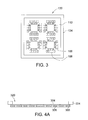
Referring to FIG. 3, a top view of the semiconductor device carrier of FIG. 1J is shown. As shown in FIG. 3, the conductive trace layer 104 and the plating ring 134 are separated from each other by the first dielectric layer 112, but such exemplification does not limit the invention. Referring to FIGS. 4A˜4B. FIG. 4A shows a cross-sectional view of a semiconductor device carrier according to another embodiment of the invention. FIG. 4B shows a top view of the semiconductor device carrier of FIG. 4A. The conductive trace layer 304 of the semiconductor device carrier 320 is electrically connected to the plating ring 334 of the semiconductor device carrier 320. Specifically, every trace 306 and every die pad 308 of the conductive trace layer 104 are interconnected and further connected electrically to the plating ring 334.
Referring to FIG. 1J, the plating conductive layer 114 is completely removed, but such exemplification does not limit the invention, and the invention is further elaborated below by other examples.
Referring to FIGS. 2A˜2B, FIGS. 2A˜2B illustrates the processes of manufacturing a semiconductor device carrier according to another embodiment of the invention are shown.
Referring to FIG. 2A, a portion of the plating conductive layer 114 is removed to form a remaining portion 114 a, wherein the remaining portion 114 a of the plating conductive layer 114 at least covers part of the conductive stud 110. In the present embodiment, the remaining portion 114 a of the plating conductive layer 114 covers the entire base surface 110 b of the conductive stud 110 and also extends onto a portion of the first dielectric surface 112 a of the first dielectric layer 112. Consequently, the area of the remaining portion 114 a of the plating conductive layer 114 is larger than that of the base surface 110 b of the conductive stud 110. Using the remaining portion 114 a as an enlarged electrical pad (bond pad) can help to improve the electrical and assembly quality. In another embodiment, the remaining portion 114 a of the plating conductive layer 114 only covers the base surface 110 b of the conductive stud 110 but not the first dielectric surface 112 a.
Referring to FIG. 2B, a second surface finishing 118 b is subsequently formed on the remaining portion 114 a of the plating conductive layer 114 preferably by electroless plating.
Referring to FIG. 2A, alternatively the remaining portion 114 a can also be considered as the second surface finishing 118 b and formed simultaneously when the plating conductive layer 114 is removed. Thus the present embodiment of the invention does not require an additional manufacturing process for forming the second surface finishing 118 b on the base surface 110 b of the conductive stud 110. After a portion of the plating conductive layer 114 is removed, the second surface finishing 118 b is also formed. Thus the formation of the semiconductor device carrier 220 is completed.
Referring to FIG. 1K to 1M, FIG. 1K to 1M illustrates the processes of manufacturing a semiconductor package using the semiconductor device carrier 220. Referring to FIG. 1K, at least one semiconductor device 122 is disposed adjacent to the conductive trace layer 104. Preferably, the semiconductor device 122 has a rear surface 122 b and an active surface 122 a opposite to the rear surface 122 b. In one instance, the rear surface 122 b of the semiconductor device 122 may be attached to the conductive trace layer 104 by means of an adhesive 128. The face-up active surface 122 a of the semiconductor device 122 is electrically connected to the trace 106 via at least one bonding wire 124 by connecting to the first surface finishing 118 a of the trace 106. In another instance, the active surface of the semiconductor device 130 is in a face-down manner and several interconnections 132 are electrically connecting the semiconductor device 130 to at least one of the die pad 108 or the trace 106 via the first surface finishing 118 a. In this case, the semiconductor device 130 is a flip-chip. In other implementation, in the absence of the first surface finishing 118 a, the interconnections 132 of the semiconductor device 130 bond directly onto at least one of the die pad 108 or the trace 106.
Referring to FIG. 1L, a second dielectric layer 126 is formed by molding to encapsulate the semiconductor device 122 and the bonding wire 124.
Referring to FIG. 1M, the second dielectric layer 126 and the first dielectric layer 112 are singulated by using a cutting tool or laser to separate the assembled semiconductor device carrier 120. Thus the formation of the semiconductor package 100 is completed.
According to the manufacturing method for a semiconductor device carrier and the manufacturing method for a semiconductor package using the same disclosed in the above embodiments of the invention, the dielectric layer of the semiconductor device carrier encapsulates the conductive trace layer and the conductive stud layer which electrically connects the two opposite sides of the semiconductor device carrier. Since no through-hole is required and the dielectric layer has a smaller thickness, the size of the semiconductor package is thus effectively reduced. Furthermore, since the surface finishing on the mutually isolated traces and die pads of the conductive trace layer is formed by electrolytic plating, the stability and reliability of the product are further increased.
While the invention has been described by way of example and in terms of the preferred embodiment(s), it is to be understood that the invention is not limited thereto. On the contrary, it is intended to cover various modifications and similar arrangements and procedures, and the scope of the appended claims therefore should be accorded the broadest interpretation so as to encompass all such modifications and similar arrangements and procedures.

Claims (28)

What is claimed is:
1. A method of manufacturing a semiconductor device carrier comprising:
providing a conductive carrier having a first surface and a second surface opposite the first surface;
forming a conductive trace layer on the second surface of the conductive carrier;
forming a conductive stud layer on the conductive trace layer;
forming a dielectric layer to encapsulate the conductive trace layer and the conductive stud layer, wherein the conductive stud layer is exposed from the dielectric layer;
forming a plating conductive layer to envelop the conductive carrier, the dielectric layer and the exposed conductive stud layer;
forming at least one cavity on the conductive carrier by removing a portion of the conductive carrier, wherein
the cavity exposes the conductive trace layer,
the remaining portion of the conductive carrier forms a plating ring around the peripheral of the dielectric layer, and
the plating ring is electrically connected to the conductive trace layer via the plating conductive layer and the conductive stud layer;
forming a first surface finishing on at least a portion of the exposed conductive trace layer in the cavity; and
removing the plating conductive layer.
2. The manufacturing method according to claim 1, wherein in the step of forming the conductive trace layer on the second surface of the conductive carrier, the conductive trace layer comprises a plurality of traces mutually isolated from one another.
3. The manufacturing method according to claim 2, wherein in the step of forming the conductive stud layer on the conductive trace layer, the conductive stud layer comprises
a plurality of studs correspondingly disposed on the plurality of traces.
4. The manufacturing method according to claim 2, wherein after the step of removing the plating conductive layer, the plurality of traces are electrically isolated from one another.
5. The manufacturing method according to claim 1, wherein the step of forming the dielectric layer comprises:
providing an encapsulant;
heating the encapsulant to a molten state;
infusing the molten encapsulant onto the second surface of the conductive carrier to encapsulate the conductive trace layer and the conductive stud layer in a high-temperature and high-pressure environment; and
solidifying the molten encapsulant to form the dielectric layer.
6. The manufacturing method according to claim 1, wherein prior to the step of forming the dielectric layer, the manufacturing method further comprises:
forming an adhesion layer on the conductive trace layer and the conductive stud layer.
7. The manufacturing method according to claim 5, wherein after the step of solidifying the molten encapsulant to form the dielectric layer, the manufacturing method further comprises:
removing part of the dielectric layer to expose the conductive stud layer from the dielectric layer.
8. The manufacturing method according to claim 5, wherein in the step of solidifying the molten encapsulant to form the dielectric layer, the conductive stud layer is exposed from the dielectric layer.
9. The manufacturing method according to claim 1, wherein the step of forming the plating conductive layer comprises:
forming a seed layer to envelop the conductive carrier, the dielectric layer and the exposed conductive stud layer; and
forming a sub-conductive layer over the seed layer.
10. The manufacturing method according to claim 1, wherein the step of forming the first surface finishing comprises:
forming the first surface finishing on all of the exposed conductive trace layer, simultaneously by electrolytic plating through the plating ring and the plating conductive layer.
11. The manufacturing method according to claim 1, wherein after the step of removing the plating conductive layer, the conductive stud layer is exposed from the dielectric layer.
12. The manufacturing method according to claim 11, wherein after the step of removing the plating conductive layer, the manufacturing method further comprises:
forming a second surface finishing on the exposed conductive stud layer.
13. The manufacturing method according to claim 1, wherein in the step of removing the plating conductive layer, a portion of the plating conductive layer is removed and a remaining portion of the plating conductive layer at least covers the conductive stud layer.
14. A method of manufacturing a semiconductor device carrier comprises:
providing a conductive carrier having a first surface and a second surface opposite the first surface;
forming a plurality of traces on the second surface of the conductive carrier;
forming a plurality of studs on the plurality of traces;
forming a dielectric layer to encapsulate the plurality of traces and the plurality of studs,
wherein the plurality of studs is exposed from the dielectric layer;
forming a plating conductive layer to envelop the conductive carrier, the dielectric layer and the exposed plurality of studs;
forming at least one cavity on the conductive carrier to expose the plurality of traces from the dielectric layer in the cavity;
forming a first surface finishing on at least a portion of the exposed plurality of traces in the cavity; and
removing the plating conductive layer.
15. The manufacturing method according to claim 14, wherein in the step of forming the plurality of traces on the second surface of the conductive carrier, the plurality of traces are mutually isolated from one another.
16. The manufacturing method according to claim 15, wherein in the step of forming the plurality of studs lay on the plurality of traces, each of the plurality of studs corresponds to at least one trace.
17. The manufacturing method according to claim 15, wherein after the step of removing the plating conductive layer, the plurality of traces are electrically isolated from one another.
18. The manufacturing method according to claim 14, wherein the step of forming the dielectric layer comprises:
providing an encapsulant;
heating the encapsulant to a molten state;
infusing the molten encapsulant onto the second surface of the conductive carrier to encapsulate the plurality of traces and the plurality of studs in under a high-temperature and high-pressure environment; and
solidifying the molten encapsulant to form the dielectric layer.
19. The manufacturing method according to claim 14, wherein prior to the step of forming the dielectric layer, the manufacturing method further comprises:
forming an adhesion layer on the plurality of traces and the plurality of studs.
20. The manufacturing method according to claim 18, wherein after the step of solidifying the molten encapsulant to form the dielectric layer, the manufacturing method further comprises:
Removing a part of the dielectric layer to expose the plurality of studs from the dielectric layer.
21. The manufacturing method according to claim 18, wherein in the step of solidifying the molten encapsulant to form the dielectric layer, the plurality of studs is exposed from the dielectric layer.
22. The manufacturing method according to claim 14, wherein the step of forming the plating conductive layer comprises:
forming a seed layer to envelop the conductive carrier, the dielectric layer and the exposed plurality of studs; and
forming a sub-conductive layer over the seed layer.
23. The manufacturing method according to claim 14, wherein the step of forming at least one cavity on the conductive carrier comprises:
removing at least a portion of the conductive carrier, wherein a remaining portion of the conductive carrier forms a plating ring around the peripheral of the dielectric layer.
24. The manufacturing method according to claim 23, wherein in the step of forming the plating ring, the plating ring is electrically connected to the plurality of traces via the plating conductive layer and the plurality of studs.
25. The manufacturing method according to claim 24, wherein the step of forming the first surface finishing comprises:
forming the first surface finishing on each of the exposed plurality of traces simultaneously, by electrolytic plating through the plating ring and the plating conductive layer.
26. The manufacturing method according to claim 14, wherein after the step of removing the plating conductive layer, the plurality of studs are exposed from the dielectric layer.
27. The manufacturing method according to claim 26, wherein after the step of removing the plating conductive layer, the manufacturing method further comprises:
forming a second surface finishing on the exposed plurality of studs.
28. The manufacturing method according to claim 14, wherein in the step of removing the plating conductive layer, a portion of the plating conductive layer is removed and a remaining portion of the plating conductive layer at least covers the plurality of studs.
US13/222,792 2010-08-31 2011-08-31 Manufacturing method for semiconductor device carrier and semiconductor package using the same Active 2032-08-08 US8709874B2 (en)

Priority Applications (3)

Application Number Priority Date Filing Date Title
US13/222,792 US8709874B2 (en) 2010-08-31 2011-08-31 Manufacturing method for semiconductor device carrier and semiconductor package using the same
US14/185,779 US9219027B2 (en) 2010-08-31 2014-02-20 Semiconductor device carrier and semiconductor package using the same
US14/961,825 US9583449B2 (en) 2010-08-31 2015-12-07 Semiconductor package

Applications Claiming Priority (2)

Application Number Priority Date Filing Date Title
US37844710P 2010-08-31 2010-08-31
US13/222,792 US8709874B2 (en) 2010-08-31 2011-08-31 Manufacturing method for semiconductor device carrier and semiconductor package using the same

Related Child Applications (1)

Application Number Title Priority Date Filing Date
US14/185,779 Division US9219027B2 (en) 2010-08-31 2014-02-20 Semiconductor device carrier and semiconductor package using the same

Publications (2)

Publication Number Publication Date
US20120058604A1 US20120058604A1 (en) 2012-03-08
US8709874B2 true US8709874B2 (en) 2014-04-29

Family

ID=45359400

Family Applications (3)

Application Number Title Priority Date Filing Date
US13/222,792 Active 2032-08-08 US8709874B2 (en) 2010-08-31 2011-08-31 Manufacturing method for semiconductor device carrier and semiconductor package using the same
US14/185,779 Active US9219027B2 (en) 2010-08-31 2014-02-20 Semiconductor device carrier and semiconductor package using the same
US14/961,825 Active US9583449B2 (en) 2010-08-31 2015-12-07 Semiconductor package

Family Applications After (2)

Application Number Title Priority Date Filing Date
US14/185,779 Active US9219027B2 (en) 2010-08-31 2014-02-20 Semiconductor device carrier and semiconductor package using the same
US14/961,825 Active US9583449B2 (en) 2010-08-31 2015-12-07 Semiconductor package

Country Status (3)

Country Link
US (3) US8709874B2 (en)
CN (2) CN103824836B (en)
TW (2) TWI543327B (en)

Cited By (2)

* Cited by examiner, † Cited by third party
Publication number Priority date Publication date Assignee Title
US20150279777A1 (en) * 2014-03-28 2015-10-01 Phoenix Pioneer Technology Co., Ltd. Package apparatus and manufacturing method thereof
US10319684B2 (en) 2017-04-11 2019-06-11 STATS ChipPAC Pte. Ltd. Dummy conductive structures for EMI shielding

Families Citing this family (20)

* Cited by examiner, † Cited by third party
Publication number Priority date Publication date Assignee Title
CN103066051B (en) * 2011-10-20 2017-03-01 先进封装技术私人有限公司 Packaging substrate and its manufacturing process, semiconductor element packaging structure and manufacturing process
TWI557855B (en) * 2011-12-30 2016-11-11 旭德科技股份有限公司 Package carrier board and manufacturing method thereof
US10049950B2 (en) * 2012-03-26 2018-08-14 Advanpack Solutions Pte Ltd Multi-layer substrate for semiconductor packaging
US8587099B1 (en) 2012-05-02 2013-11-19 Texas Instruments Incorporated Leadframe having selective planishing
US9177899B2 (en) 2012-07-31 2015-11-03 Mediatek Inc. Semiconductor package and method for fabricating base for semiconductor package
US10991669B2 (en) 2012-07-31 2021-04-27 Mediatek Inc. Semiconductor package using flip-chip technology
TWI562295B (en) 2012-07-31 2016-12-11 Mediatek Inc Semiconductor package and method for fabricating base for semiconductor package
US20160056098A9 (en) * 2012-09-28 2016-02-25 Yan Xun Xue Semiconductor device employing aluminum alloy lead-frame with anodized aluminum
TWI471990B (en) * 2012-11-05 2015-02-01 矽品精密工業股份有限公司 Method for manufacturing carrier and semiconductor package for fixing semiconductor package
WO2014112954A1 (en) * 2013-01-21 2014-07-24 Pbt Pte. Ltd. Substrate for semiconductor packaging and method of forming same
US9754899B2 (en) 2013-02-21 2017-09-05 Advanpack Solutions Pte Ltd Semiconductor structure and method of fabricating the same
US9142530B2 (en) 2013-03-21 2015-09-22 Stats Chippac Ltd. Coreless integrated circuit packaging system and method of manufacture thereof
CN104064542B (en) * 2013-03-21 2018-04-27 新科金朋有限公司 Coreless integrated circuit package system and its manufacture method
US9257370B2 (en) * 2013-08-27 2016-02-09 Ubotic Company Limited Cavity package with pre-molded cavity leadframe
EP2843698A3 (en) 2013-08-27 2015-04-01 Ubotic Company Limited Cavity package with pre-molded substrate
TWI581386B (en) * 2014-06-16 2017-05-01 恆勁科技股份有限公司 Package apparatus and manufacturing method thereof
TWI474417B (en) * 2014-06-16 2015-02-21 恆勁科技股份有限公司 Packaging method
TWI591762B (en) * 2014-06-30 2017-07-11 恆勁科技股份有限公司 Packaging device and manufacturing method thereof
US20160099200A1 (en) * 2014-10-01 2016-04-07 Stmicroelectronics S.R.L. Aluminum alloy lead frame for a semiconductor device and corresponding manufacturing process
TWI569368B (en) 2015-03-06 2017-02-01 恆勁科技股份有限公司 Package substrate, package structure including the same, and manufacturing method thereof

Citations (5)

* Cited by examiner, † Cited by third party
Publication number Priority date Publication date Assignee Title
US20060094158A1 (en) * 2004-10-28 2006-05-04 Samsung Electronics Co., Ltd. Fabrication method of packaging substrate and packaging method using the packaging substrate
US7790505B2 (en) * 2006-10-18 2010-09-07 Advanced Semiconductor Engineering, Inc. Semiconductor chip package manufacturing method and structure thereof
US7915080B2 (en) * 2008-12-19 2011-03-29 Texas Instruments Incorporated Bonding IC die to TSV wafers
US8159828B2 (en) * 2007-02-23 2012-04-17 Alpha & Omega Semiconductor, Inc. Low profile flip chip power module and method of making
US8338232B2 (en) * 2010-12-28 2012-12-25 Alpha & Omega Semiconductor, Inc. Power semiconductor device package method

Family Cites Families (14)

* Cited by examiner, † Cited by third party
Publication number Priority date Publication date Assignee Title
CN1516251A (en) * 1994-03-18 2004-07-28 �������ɹ�ҵ��ʽ���� Manufacturing method of semiconductor component and semiconductor component
JP2581017B2 (en) * 1994-09-30 1997-02-12 日本電気株式会社 Semiconductor device and manufacturing method thereof
KR100218996B1 (en) * 1995-03-24 1999-09-01 모기 쥰이찌 Semiconductor device
JP3264147B2 (en) * 1995-07-18 2002-03-11 日立電線株式会社 Semiconductor device, interposer for semiconductor device, and method of manufacturing the same
JP3176542B2 (en) * 1995-10-25 2001-06-18 シャープ株式会社 Semiconductor device and manufacturing method thereof
EP0791960A3 (en) * 1996-02-23 1998-02-18 Matsushita Electric Industrial Co., Ltd. Semiconductor devices having protruding contacts and method for making the same
JP3437369B2 (en) * 1996-03-19 2003-08-18 松下電器産業株式会社 Chip carrier and semiconductor device using the same
US6064111A (en) * 1996-07-31 2000-05-16 Hitachi Company, Ltd. Substrate for holding a chip of semi-conductor package, semi-conductor package, and fabrication process of semi-conductor package
US6060777A (en) * 1998-07-21 2000-05-09 Intel Corporation Underside heat slug for ball grid array packages
TW473962B (en) * 2001-01-20 2002-01-21 Siliconware Precision Industries Co Ltd Cavity down ball grid array package and its manufacturing process
US7259448B2 (en) * 2001-05-07 2007-08-21 Broadcom Corporation Die-up ball grid array package with a heat spreader and method for making the same
US6537848B2 (en) * 2001-05-30 2003-03-25 St. Assembly Test Services Ltd. Super thin/super thermal ball grid array package
US6879039B2 (en) * 2001-12-18 2005-04-12 Broadcom Corporation Ball grid array package substrates and method of making the same
US6861750B2 (en) * 2002-02-01 2005-03-01 Broadcom Corporation Ball grid array package with multiple interposers

Patent Citations (5)

* Cited by examiner, † Cited by third party
Publication number Priority date Publication date Assignee Title
US20060094158A1 (en) * 2004-10-28 2006-05-04 Samsung Electronics Co., Ltd. Fabrication method of packaging substrate and packaging method using the packaging substrate
US7790505B2 (en) * 2006-10-18 2010-09-07 Advanced Semiconductor Engineering, Inc. Semiconductor chip package manufacturing method and structure thereof
US8159828B2 (en) * 2007-02-23 2012-04-17 Alpha & Omega Semiconductor, Inc. Low profile flip chip power module and method of making
US7915080B2 (en) * 2008-12-19 2011-03-29 Texas Instruments Incorporated Bonding IC die to TSV wafers
US8338232B2 (en) * 2010-12-28 2012-12-25 Alpha & Omega Semiconductor, Inc. Power semiconductor device package method

Cited By (4)

* Cited by examiner, † Cited by third party
Publication number Priority date Publication date Assignee Title
US20150279777A1 (en) * 2014-03-28 2015-10-01 Phoenix Pioneer Technology Co., Ltd. Package apparatus and manufacturing method thereof
US9750142B2 (en) * 2014-03-28 2017-08-29 Phoenix Pioneer Technology Co., Ltd. Method for manufacturing an electronic package
US11246223B2 (en) 2014-03-28 2022-02-08 Phoenix Pioneer Technology Co., Ltd. Package apparatus
US10319684B2 (en) 2017-04-11 2019-06-11 STATS ChipPAC Pte. Ltd. Dummy conductive structures for EMI shielding

Also Published As

Publication number Publication date
US20120058604A1 (en) 2012-03-08
CN102299082A (en) 2011-12-28
CN103824836B (en) 2017-03-01
TW201419486A (en) 2014-05-16
US20160118349A1 (en) 2016-04-28
US20140167240A1 (en) 2014-06-19
US9219027B2 (en) 2015-12-22
TWI429048B (en) 2014-03-01
TW201209983A (en) 2012-03-01
TWI543327B (en) 2016-07-21
CN103824836A (en) 2014-05-28
CN102299082B (en) 2014-04-16
US9583449B2 (en) 2017-02-28

Similar Documents

Publication Publication Date Title
US8709874B2 (en) Manufacturing method for semiconductor device carrier and semiconductor package using the same
US12451441B2 (en) Semiconductor device having EMI shielding structure and related methods
CN107017238B (en) Electronic device
TWI527175B (en) Semiconductor package, substrate and method of manufacturing same
TW200818458A (en) Stackable packages for three-dimensional packaging of semiconductor dice
CN111293112B (en) Semiconductor package and method of manufacturing the same
TW201145411A (en) Semiconductor package without carrier and method of fabricating the same
US8569885B2 (en) Stacked semiconductor packages and related methods
US12334420B2 (en) Semiconductor devices and methods of manufacturing semiconductor devices
CN105514086B (en) Semiconductor package and manufacturing method thereof
US20160155716A1 (en) Package substrate, semiconductor package and method of manufacturing the same
TW201705426A (en) Resin sealed type semiconductor device and method of manufacturing same
US8796867B2 (en) Semiconductor package and fabrication method thereof
TWI596731B (en) Use electroless Z-connection
CN102280431A (en) Semiconductor package with protective layer and manufacturing method thereof
KR20090096184A (en) Semiconductor package
US7868449B2 (en) Semiconductor substrate and method of connecting semiconductor die to substrate
JP2008198916A (en) Semiconductor device and manufacturing method thereof
TWI456718B (en) Package structure and its manufacturing method
US20230110079A1 (en) Fan-out package structure and manufacturing method thereof
KR20240057505A (en) Method for manufacturing semiconductor device and semiconductor device thereto
CN107978584B (en) Chip packaging structure and manufacturing method thereof
TW202027243A (en) Package structure and manufacturing method thereof
JP2010187037A (en) Method of manufacturing semiconductor device
CN102487019A (en) Method for manufacturing chip packaging piece

Legal Events

Date Code Title Description
AS Assignment

Owner name: ADVANPACK SOLUTIONS PTE LTD., SINGAPORE

Free format text: ASSIGNMENT OF ASSIGNORS INTEREST;ASSIGNORS:CHEW, HWEE-SENG JIMMY;LIM, KIAN-HOCK;FORTALEZA, OVISO DOMINADOR JR;AND OTHERS;REEL/FRAME:026839/0780

Effective date: 20110824

STCF Information on status: patent grant

Free format text: PATENTED CASE

MAFP Maintenance fee payment

Free format text: PAYMENT OF MAINTENANCE FEE, 4TH YR, SMALL ENTITY (ORIGINAL EVENT CODE: M2551)

Year of fee payment: 4

MAFP Maintenance fee payment

Free format text: PAYMENT OF MAINTENANCE FEE, 8TH YR, SMALL ENTITY (ORIGINAL EVENT CODE: M2552); ENTITY STATUS OF PATENT OWNER: SMALL ENTITY

Year of fee payment: 8

MAFP Maintenance fee payment

Free format text: PAYMENT OF MAINTENANCE FEE, 12TH YR, SMALL ENTITY (ORIGINAL EVENT CODE: M2553); ENTITY STATUS OF PATENT OWNER: SMALL ENTITY

Year of fee payment: 12