US8643113B2 - Structure and method for metal gate stack oxygen concentration control using an oxygen diffusion barrier layer and a sacrificial oxygen gettering layer - Google Patents
Structure and method for metal gate stack oxygen concentration control using an oxygen diffusion barrier layer and a sacrificial oxygen gettering layer Download PDFInfo
- Publication number
- US8643113B2 US8643113B2 US12/275,812 US27581208A US8643113B2 US 8643113 B2 US8643113 B2 US 8643113B2 US 27581208 A US27581208 A US 27581208A US 8643113 B2 US8643113 B2 US 8643113B2
- Authority
- US
- United States
- Prior art keywords
- nmos
- work function
- layer
- pmos
- gate
- Prior art date
- Legal status (The legal status is an assumption and is not a legal conclusion. Google has not performed a legal analysis and makes no representation as to the accuracy of the status listed.)
- Active, expires
Links
- 229910052751 metal Inorganic materials 0.000 title claims abstract description 137
- 239000002184 metal Substances 0.000 title claims abstract description 137
- 239000001301 oxygen Substances 0.000 title claims abstract description 62
- 229910052760 oxygen Inorganic materials 0.000 title claims abstract description 62
- QVGXLLKOCUKJST-UHFFFAOYSA-N atomic oxygen Chemical compound [O] QVGXLLKOCUKJST-UHFFFAOYSA-N 0.000 title claims abstract description 61
- 238000009792 diffusion process Methods 0.000 title claims abstract description 30
- 230000004888 barrier function Effects 0.000 title claims description 25
- 238000000034 method Methods 0.000 title abstract description 71
- 238000005247 gettering Methods 0.000 title abstract description 5
- 125000004429 atom Chemical group 0.000 claims description 21
- 125000004430 oxygen atom Chemical group O* 0.000 claims description 19
- 239000000758 substrate Substances 0.000 claims description 15
- VYPSYNLAJGMNEJ-UHFFFAOYSA-N Silicium dioxide Chemical compound O=[Si]=O VYPSYNLAJGMNEJ-UHFFFAOYSA-N 0.000 claims description 7
- 238000009826 distribution Methods 0.000 claims description 7
- 229910052581 Si3N4 Inorganic materials 0.000 claims description 6
- 229910052814 silicon oxide Inorganic materials 0.000 claims description 6
- 239000000203 mixture Substances 0.000 claims description 5
- 239000007769 metal material Substances 0.000 claims description 4
- 229910004129 HfSiO Inorganic materials 0.000 claims description 3
- 229910006501 ZrSiO Inorganic materials 0.000 claims description 3
- ATJFFYVFTNAWJD-UHFFFAOYSA-N Tin Chemical compound [Sn] ATJFFYVFTNAWJD-UHFFFAOYSA-N 0.000 claims 4
- PNEYBMLMFCGWSK-UHFFFAOYSA-N aluminium oxide Inorganic materials [O-2].[O-2].[O-2].[Al+3].[Al+3] PNEYBMLMFCGWSK-UHFFFAOYSA-N 0.000 claims 2
- 229910052593 corundum Inorganic materials 0.000 claims 2
- 229910001845 yogo sapphire Inorganic materials 0.000 claims 2
- 229910017109 AlON Inorganic materials 0.000 claims 1
- 229910004140 HfO Inorganic materials 0.000 claims 1
- -1 HfSiON Inorganic materials 0.000 claims 1
- 239000000463 material Substances 0.000 abstract description 27
- 230000003647 oxidation Effects 0.000 abstract description 10
- 238000007254 oxidation reaction Methods 0.000 abstract description 10
- 230000000903 blocking effect Effects 0.000 abstract description 4
- 239000000284 extract Substances 0.000 abstract description 2
- 125000006850 spacer group Chemical group 0.000 description 13
- 230000015572 biosynthetic process Effects 0.000 description 12
- XUIMIQQOPSSXEZ-UHFFFAOYSA-N Silicon Chemical compound [Si] XUIMIQQOPSSXEZ-UHFFFAOYSA-N 0.000 description 9
- 238000005229 chemical vapour deposition Methods 0.000 description 9
- 229910052710 silicon Inorganic materials 0.000 description 9
- 239000010703 silicon Substances 0.000 description 9
- 238000000151 deposition Methods 0.000 description 8
- 238000000231 atomic layer deposition Methods 0.000 description 7
- 238000005240 physical vapour deposition Methods 0.000 description 7
- 229910021332 silicide Inorganic materials 0.000 description 7
- FVBUAEGBCNSCDD-UHFFFAOYSA-N silicide(4-) Chemical compound [Si-4] FVBUAEGBCNSCDD-UHFFFAOYSA-N 0.000 description 7
- IJGRMHOSHXDMSA-UHFFFAOYSA-N Atomic nitrogen Chemical compound N#N IJGRMHOSHXDMSA-UHFFFAOYSA-N 0.000 description 6
- 239000002019 doping agent Substances 0.000 description 6
- HQVNEWCFYHHQES-UHFFFAOYSA-N silicon nitride Chemical compound N12[Si]34N5[Si]62N3[Si]51N64 HQVNEWCFYHHQES-UHFFFAOYSA-N 0.000 description 5
- VHUUQVKOLVNVRT-UHFFFAOYSA-N Ammonium hydroxide Chemical compound [NH4+].[OH-] VHUUQVKOLVNVRT-UHFFFAOYSA-N 0.000 description 4
- XKRFYHLGVUSROY-UHFFFAOYSA-N Argon Chemical compound [Ar] XKRFYHLGVUSROY-UHFFFAOYSA-N 0.000 description 4
- MHAJPDPJQMAIIY-UHFFFAOYSA-N Hydrogen peroxide Chemical compound OO MHAJPDPJQMAIIY-UHFFFAOYSA-N 0.000 description 4
- MWUXSHHQAYIFBG-UHFFFAOYSA-N Nitric oxide Chemical compound O=[N] MWUXSHHQAYIFBG-UHFFFAOYSA-N 0.000 description 4
- GQPLMRYTRLFLPF-UHFFFAOYSA-N Nitrous Oxide Chemical compound [O-][N+]#N GQPLMRYTRLFLPF-UHFFFAOYSA-N 0.000 description 4
- 150000002500 ions Chemical class 0.000 description 4
- 238000004519 manufacturing process Methods 0.000 description 4
- 229920002120 photoresistant polymer Polymers 0.000 description 4
- 239000004065 semiconductor Substances 0.000 description 4
- 239000000126 substance Substances 0.000 description 4
- WGTYBPLFGIVFAS-UHFFFAOYSA-M tetramethylammonium hydroxide Chemical compound [OH-].C[N+](C)(C)C WGTYBPLFGIVFAS-UHFFFAOYSA-M 0.000 description 4
- YCKRFDGAMUMZLT-UHFFFAOYSA-N Fluorine atom Chemical compound [F] YCKRFDGAMUMZLT-UHFFFAOYSA-N 0.000 description 3
- CBENFWSGALASAD-UHFFFAOYSA-N Ozone Chemical compound [O-][O+]=O CBENFWSGALASAD-UHFFFAOYSA-N 0.000 description 3
- BOTDANWDWHJENH-UHFFFAOYSA-N Tetraethyl orthosilicate Chemical group CCO[Si](OCC)(OCC)OCC BOTDANWDWHJENH-UHFFFAOYSA-N 0.000 description 3
- 229910052782 aluminium Inorganic materials 0.000 description 3
- XAGFODPZIPBFFR-UHFFFAOYSA-N aluminium Chemical compound [Al] XAGFODPZIPBFFR-UHFFFAOYSA-N 0.000 description 3
- 230000008021 deposition Effects 0.000 description 3
- 229910052731 fluorine Inorganic materials 0.000 description 3
- 239000011737 fluorine Substances 0.000 description 3
- 229910044991 metal oxide Inorganic materials 0.000 description 3
- 150000004706 metal oxides Chemical class 0.000 description 3
- NFFIWVVINABMKP-UHFFFAOYSA-N methylidynetantalum Chemical compound [Ta]#C NFFIWVVINABMKP-UHFFFAOYSA-N 0.000 description 3
- 229910052757 nitrogen Inorganic materials 0.000 description 3
- 238000000623 plasma-assisted chemical vapour deposition Methods 0.000 description 3
- 229910003468 tantalcarbide Inorganic materials 0.000 description 3
- ZAMOUSCENKQFHK-UHFFFAOYSA-N Chlorine atom Chemical compound [Cl] ZAMOUSCENKQFHK-UHFFFAOYSA-N 0.000 description 2
- PXHVJJICTQNCMI-UHFFFAOYSA-N Nickel Chemical compound [Ni] PXHVJJICTQNCMI-UHFFFAOYSA-N 0.000 description 2
- OAICVXFJPJFONN-UHFFFAOYSA-N Phosphorus Chemical compound [P] OAICVXFJPJFONN-UHFFFAOYSA-N 0.000 description 2
- RTAQQCXQSZGOHL-UHFFFAOYSA-N Titanium Chemical compound [Ti] RTAQQCXQSZGOHL-UHFFFAOYSA-N 0.000 description 2
- NRTOMJZYCJJWKI-UHFFFAOYSA-N Titanium nitride Chemical compound [Ti]#N NRTOMJZYCJJWKI-UHFFFAOYSA-N 0.000 description 2
- 229910052786 argon Inorganic materials 0.000 description 2
- 238000001505 atmospheric-pressure chemical vapour deposition Methods 0.000 description 2
- 239000000460 chlorine Substances 0.000 description 2
- 229910052801 chlorine Inorganic materials 0.000 description 2
- 238000005137 deposition process Methods 0.000 description 2
- 239000003989 dielectric material Substances 0.000 description 2
- 230000000694 effects Effects 0.000 description 2
- 239000007789 gas Substances 0.000 description 2
- 229910052735 hafnium Inorganic materials 0.000 description 2
- VBJZVLUMGGDVMO-UHFFFAOYSA-N hafnium atom Chemical compound [Hf] VBJZVLUMGGDVMO-UHFFFAOYSA-N 0.000 description 2
- 229910000449 hafnium oxide Inorganic materials 0.000 description 2
- 239000001257 hydrogen Substances 0.000 description 2
- 229910052739 hydrogen Inorganic materials 0.000 description 2
- 238000004518 low pressure chemical vapour deposition Methods 0.000 description 2
- QJGQUHMNIGDVPM-UHFFFAOYSA-N nitrogen group Chemical group [N] QJGQUHMNIGDVPM-UHFFFAOYSA-N 0.000 description 2
- 239000001272 nitrous oxide Substances 0.000 description 2
- TWNQGVIAIRXVLR-UHFFFAOYSA-N oxo(oxoalumanyloxy)alumane Chemical compound O=[Al]O[Al]=O TWNQGVIAIRXVLR-UHFFFAOYSA-N 0.000 description 2
- 229910052698 phosphorus Inorganic materials 0.000 description 2
- 239000011574 phosphorus Substances 0.000 description 2
- 229910021420 polycrystalline silicon Inorganic materials 0.000 description 2
- 238000005381 potential energy Methods 0.000 description 2
- MZLGASXMSKOWSE-UHFFFAOYSA-N tantalum nitride Chemical compound [Ta]#N MZLGASXMSKOWSE-UHFFFAOYSA-N 0.000 description 2
- 239000010936 titanium Substances 0.000 description 2
- 229910052719 titanium Inorganic materials 0.000 description 2
- MTPVUVINMAGMJL-UHFFFAOYSA-N trimethyl(1,1,2,2,2-pentafluoroethyl)silane Chemical compound C[Si](C)(C)C(F)(F)C(F)(F)F MTPVUVINMAGMJL-UHFFFAOYSA-N 0.000 description 2
- RPAJSBKBKSSMLJ-DFWYDOINSA-N (2s)-2-aminopentanedioic acid;hydrochloride Chemical class Cl.OC(=O)[C@@H](N)CCC(O)=O RPAJSBKBKSSMLJ-DFWYDOINSA-N 0.000 description 1
- ZOXJGFHDIHLPTG-UHFFFAOYSA-N Boron Chemical compound [B] ZOXJGFHDIHLPTG-UHFFFAOYSA-N 0.000 description 1
- 229910052684 Cerium Inorganic materials 0.000 description 1
- GYHNNYVSQQEPJS-UHFFFAOYSA-N Gallium Chemical compound [Ga] GYHNNYVSQQEPJS-UHFFFAOYSA-N 0.000 description 1
- UFHFLCQGNIYNRP-UHFFFAOYSA-N Hydrogen Chemical compound [H][H] UFHFLCQGNIYNRP-UHFFFAOYSA-N 0.000 description 1
- BPQQTUXANYXVAA-UHFFFAOYSA-N Orthosilicate Chemical compound [O-][Si]([O-])([O-])[O-] BPQQTUXANYXVAA-UHFFFAOYSA-N 0.000 description 1
- GEIAQOFPUVMAGM-UHFFFAOYSA-N Oxozirconium Chemical compound [Zr]=O GEIAQOFPUVMAGM-UHFFFAOYSA-N 0.000 description 1
- 229910000577 Silicon-germanium Inorganic materials 0.000 description 1
- QCWXUUIWCKQGHC-UHFFFAOYSA-N Zirconium Chemical compound [Zr] QCWXUUIWCKQGHC-UHFFFAOYSA-N 0.000 description 1
- LEVVHYCKPQWKOP-UHFFFAOYSA-N [Si].[Ge] Chemical compound [Si].[Ge] LEVVHYCKPQWKOP-UHFFFAOYSA-N 0.000 description 1
- CEPICIBPGDWCRU-UHFFFAOYSA-N [Si].[Hf] Chemical compound [Si].[Hf] CEPICIBPGDWCRU-UHFFFAOYSA-N 0.000 description 1
- 239000002253 acid Substances 0.000 description 1
- 239000000908 ammonium hydroxide Substances 0.000 description 1
- 239000007864 aqueous solution Substances 0.000 description 1
- 229910052785 arsenic Inorganic materials 0.000 description 1
- RQNWIZPPADIBDY-UHFFFAOYSA-N arsenic atom Chemical compound [As] RQNWIZPPADIBDY-UHFFFAOYSA-N 0.000 description 1
- IVHJCRXBQPGLOV-UHFFFAOYSA-N azanylidynetungsten Chemical compound [W]#N IVHJCRXBQPGLOV-UHFFFAOYSA-N 0.000 description 1
- 229910052796 boron Inorganic materials 0.000 description 1
- GWXLDORMOJMVQZ-UHFFFAOYSA-N cerium Chemical compound [Ce] GWXLDORMOJMVQZ-UHFFFAOYSA-N 0.000 description 1
- 238000006243 chemical reaction Methods 0.000 description 1
- OEYIOHPDSNJKLS-UHFFFAOYSA-N choline Chemical compound C[N+](C)(C)CCO OEYIOHPDSNJKLS-UHFFFAOYSA-N 0.000 description 1
- 229960001231 choline Drugs 0.000 description 1
- 239000010941 cobalt Substances 0.000 description 1
- 229910017052 cobalt Inorganic materials 0.000 description 1
- GUTLYIVDDKVIGB-UHFFFAOYSA-N cobalt atom Chemical compound [Co] GUTLYIVDDKVIGB-UHFFFAOYSA-N 0.000 description 1
- 239000013078 crystal Substances 0.000 description 1
- 238000005516 engineering process Methods 0.000 description 1
- 238000005530 etching Methods 0.000 description 1
- 239000010408 film Substances 0.000 description 1
- 229910052733 gallium Inorganic materials 0.000 description 1
- WIHZLLGSGQNAGK-UHFFFAOYSA-N hafnium(4+);oxygen(2-) Chemical compound [O-2].[O-2].[Hf+4] WIHZLLGSGQNAGK-UHFFFAOYSA-N 0.000 description 1
- 238000010438 heat treatment Methods 0.000 description 1
- 125000004435 hydrogen atom Chemical class [H]* 0.000 description 1
- 238000007654 immersion Methods 0.000 description 1
- 239000011261 inert gas Substances 0.000 description 1
- 239000011810 insulating material Substances 0.000 description 1
- 239000012212 insulator Substances 0.000 description 1
- 229910052746 lanthanum Inorganic materials 0.000 description 1
- FZLIPJUXYLNCLC-UHFFFAOYSA-N lanthanum atom Chemical compound [La] FZLIPJUXYLNCLC-UHFFFAOYSA-N 0.000 description 1
- 229910021421 monocrystalline silicon Inorganic materials 0.000 description 1
- 229910052759 nickel Inorganic materials 0.000 description 1
- 230000001590 oxidative effect Effects 0.000 description 1
- 229920005591 polysilicon Polymers 0.000 description 1
- HBMJWWWQQXIZIP-UHFFFAOYSA-N silicon carbide Chemical compound [Si+]#[C-] HBMJWWWQQXIZIP-UHFFFAOYSA-N 0.000 description 1
- 239000000377 silicon dioxide Substances 0.000 description 1
- 235000012239 silicon dioxide Nutrition 0.000 description 1
- UVGLBOPDEUYYCS-UHFFFAOYSA-N silicon zirconium Chemical compound [Si].[Zr] UVGLBOPDEUYYCS-UHFFFAOYSA-N 0.000 description 1
- 229910052715 tantalum Inorganic materials 0.000 description 1
- GUVRBAGPIYLISA-UHFFFAOYSA-N tantalum atom Chemical compound [Ta] GUVRBAGPIYLISA-UHFFFAOYSA-N 0.000 description 1
- 238000002230 thermal chemical vapour deposition Methods 0.000 description 1
- 238000001029 thermal curing Methods 0.000 description 1
- 238000005979 thermal decomposition reaction Methods 0.000 description 1
- 239000010409 thin film Substances 0.000 description 1
- WFKWXMTUELFFGS-UHFFFAOYSA-N tungsten Chemical compound [W] WFKWXMTUELFFGS-UHFFFAOYSA-N 0.000 description 1
- 229910052721 tungsten Inorganic materials 0.000 description 1
- 239000010937 tungsten Substances 0.000 description 1
- UONOETXJSWQNOL-UHFFFAOYSA-N tungsten carbide Chemical compound [W+]#[C-] UONOETXJSWQNOL-UHFFFAOYSA-N 0.000 description 1
- 229910052726 zirconium Inorganic materials 0.000 description 1
- GFQYVLUOOAAOGM-UHFFFAOYSA-N zirconium(iv) silicate Chemical compound [Zr+4].[O-][Si]([O-])([O-])[O-] GFQYVLUOOAAOGM-UHFFFAOYSA-N 0.000 description 1
Images


Classifications
-
- H—ELECTRICITY
- H01—ELECTRIC ELEMENTS
- H01L—SEMICONDUCTOR DEVICES NOT COVERED BY CLASS H10
- H01L21/00—Processes or apparatus adapted for the manufacture or treatment of semiconductor or solid state devices or of parts thereof
- H01L21/70—Manufacture or treatment of devices consisting of a plurality of solid state components formed in or on a common substrate or of parts thereof; Manufacture of integrated circuit devices or of parts thereof
- H01L21/77—Manufacture or treatment of devices consisting of a plurality of solid state components or integrated circuits formed in, or on, a common substrate
- H01L21/78—Manufacture or treatment of devices consisting of a plurality of solid state components or integrated circuits formed in, or on, a common substrate with subsequent division of the substrate into plural individual devices
- H01L21/82—Manufacture or treatment of devices consisting of a plurality of solid state components or integrated circuits formed in, or on, a common substrate with subsequent division of the substrate into plural individual devices to produce devices, e.g. integrated circuits, each consisting of a plurality of components
- H01L21/822—Manufacture or treatment of devices consisting of a plurality of solid state components or integrated circuits formed in, or on, a common substrate with subsequent division of the substrate into plural individual devices to produce devices, e.g. integrated circuits, each consisting of a plurality of components the substrate being a semiconductor, using silicon technology
- H01L21/8232—Field-effect technology
- H01L21/8234—MIS technology, i.e. integration processes of field effect transistors of the conductor-insulator-semiconductor type
- H01L21/8238—Complementary field-effect transistors, e.g. CMOS
- H01L21/823828—Complementary field-effect transistors, e.g. CMOS with a particular manufacturing method of the gate conductors, e.g. particular materials, shapes
- H01L21/823842—Complementary field-effect transistors, e.g. CMOS with a particular manufacturing method of the gate conductors, e.g. particular materials, shapes gate conductors with different gate conductor materials or different gate conductor implants, e.g. dual gate structures
-
- H—ELECTRICITY
- H01—ELECTRIC ELEMENTS
- H01L—SEMICONDUCTOR DEVICES NOT COVERED BY CLASS H10
- H01L21/00—Processes or apparatus adapted for the manufacture or treatment of semiconductor or solid state devices or of parts thereof
- H01L21/02—Manufacture or treatment of semiconductor devices or of parts thereof
- H01L21/04—Manufacture or treatment of semiconductor devices or of parts thereof the devices having at least one potential-jump barrier or surface barrier, e.g. PN junction, depletion layer or carrier concentration layer
- H01L21/18—Manufacture or treatment of semiconductor devices or of parts thereof the devices having at least one potential-jump barrier or surface barrier, e.g. PN junction, depletion layer or carrier concentration layer the devices having semiconductor bodies comprising elements of Group IV of the Periodic System or AIIIBV compounds with or without impurities, e.g. doping materials
- H01L21/28—Manufacture of electrodes on semiconductor bodies using processes or apparatus not provided for in groups H01L21/20 - H01L21/268
- H01L21/28008—Making conductor-insulator-semiconductor electrodes
- H01L21/28017—Making conductor-insulator-semiconductor electrodes the insulator being formed after the semiconductor body, the semiconductor being silicon
- H01L21/28026—Making conductor-insulator-semiconductor electrodes the insulator being formed after the semiconductor body, the semiconductor being silicon characterised by the conductor
- H01L21/28088—Making conductor-insulator-semiconductor electrodes the insulator being formed after the semiconductor body, the semiconductor being silicon characterised by the conductor the final conductor layer next to the insulator being a composite, e.g. TiN
-
- H—ELECTRICITY
- H01—ELECTRIC ELEMENTS
- H01L—SEMICONDUCTOR DEVICES NOT COVERED BY CLASS H10
- H01L21/00—Processes or apparatus adapted for the manufacture or treatment of semiconductor or solid state devices or of parts thereof
- H01L21/02—Manufacture or treatment of semiconductor devices or of parts thereof
- H01L21/04—Manufacture or treatment of semiconductor devices or of parts thereof the devices having at least one potential-jump barrier or surface barrier, e.g. PN junction, depletion layer or carrier concentration layer
- H01L21/18—Manufacture or treatment of semiconductor devices or of parts thereof the devices having at least one potential-jump barrier or surface barrier, e.g. PN junction, depletion layer or carrier concentration layer the devices having semiconductor bodies comprising elements of Group IV of the Periodic System or AIIIBV compounds with or without impurities, e.g. doping materials
- H01L21/28—Manufacture of electrodes on semiconductor bodies using processes or apparatus not provided for in groups H01L21/20 - H01L21/268
- H01L21/28008—Making conductor-insulator-semiconductor electrodes
- H01L21/28017—Making conductor-insulator-semiconductor electrodes the insulator being formed after the semiconductor body, the semiconductor being silicon
- H01L21/28158—Making the insulator
- H01L21/28167—Making the insulator on single crystalline silicon, e.g. using a liquid, i.e. chemical oxidation
- H01L21/28185—Making the insulator on single crystalline silicon, e.g. using a liquid, i.e. chemical oxidation with a treatment, e.g. annealing, after the formation of the gate insulator and before the formation of the definitive gate conductor
-
- H—ELECTRICITY
- H01—ELECTRIC ELEMENTS
- H01L—SEMICONDUCTOR DEVICES NOT COVERED BY CLASS H10
- H01L21/00—Processes or apparatus adapted for the manufacture or treatment of semiconductor or solid state devices or of parts thereof
- H01L21/02—Manufacture or treatment of semiconductor devices or of parts thereof
- H01L21/04—Manufacture or treatment of semiconductor devices or of parts thereof the devices having at least one potential-jump barrier or surface barrier, e.g. PN junction, depletion layer or carrier concentration layer
- H01L21/18—Manufacture or treatment of semiconductor devices or of parts thereof the devices having at least one potential-jump barrier or surface barrier, e.g. PN junction, depletion layer or carrier concentration layer the devices having semiconductor bodies comprising elements of Group IV of the Periodic System or AIIIBV compounds with or without impurities, e.g. doping materials
- H01L21/30—Treatment of semiconductor bodies using processes or apparatus not provided for in groups H01L21/20 - H01L21/26
- H01L21/322—Treatment of semiconductor bodies using processes or apparatus not provided for in groups H01L21/20 - H01L21/26 to modify their internal properties, e.g. to produce internal imperfections
- H01L21/3221—Treatment of semiconductor bodies using processes or apparatus not provided for in groups H01L21/20 - H01L21/26 to modify their internal properties, e.g. to produce internal imperfections of silicon bodies, e.g. for gettering
-
- H—ELECTRICITY
- H01—ELECTRIC ELEMENTS
- H01L—SEMICONDUCTOR DEVICES NOT COVERED BY CLASS H10
- H01L21/00—Processes or apparatus adapted for the manufacture or treatment of semiconductor or solid state devices or of parts thereof
- H01L21/70—Manufacture or treatment of devices consisting of a plurality of solid state components formed in or on a common substrate or of parts thereof; Manufacture of integrated circuit devices or of parts thereof
- H01L21/77—Manufacture or treatment of devices consisting of a plurality of solid state components or integrated circuits formed in, or on, a common substrate
- H01L21/78—Manufacture or treatment of devices consisting of a plurality of solid state components or integrated circuits formed in, or on, a common substrate with subsequent division of the substrate into plural individual devices
- H01L21/82—Manufacture or treatment of devices consisting of a plurality of solid state components or integrated circuits formed in, or on, a common substrate with subsequent division of the substrate into plural individual devices to produce devices, e.g. integrated circuits, each consisting of a plurality of components
- H01L21/822—Manufacture or treatment of devices consisting of a plurality of solid state components or integrated circuits formed in, or on, a common substrate with subsequent division of the substrate into plural individual devices to produce devices, e.g. integrated circuits, each consisting of a plurality of components the substrate being a semiconductor, using silicon technology
- H01L21/8232—Field-effect technology
- H01L21/8234—MIS technology, i.e. integration processes of field effect transistors of the conductor-insulator-semiconductor type
- H01L21/8238—Complementary field-effect transistors, e.g. CMOS
- H01L21/823807—Complementary field-effect transistors, e.g. CMOS with a particular manufacturing method of the channel structures, e.g. channel implants, halo or pocket implants, or channel materials
-
- H—ELECTRICITY
- H01—ELECTRIC ELEMENTS
- H01L—SEMICONDUCTOR DEVICES NOT COVERED BY CLASS H10
- H01L21/00—Processes or apparatus adapted for the manufacture or treatment of semiconductor or solid state devices or of parts thereof
- H01L21/70—Manufacture or treatment of devices consisting of a plurality of solid state components formed in or on a common substrate or of parts thereof; Manufacture of integrated circuit devices or of parts thereof
- H01L21/77—Manufacture or treatment of devices consisting of a plurality of solid state components or integrated circuits formed in, or on, a common substrate
- H01L21/78—Manufacture or treatment of devices consisting of a plurality of solid state components or integrated circuits formed in, or on, a common substrate with subsequent division of the substrate into plural individual devices
- H01L21/82—Manufacture or treatment of devices consisting of a plurality of solid state components or integrated circuits formed in, or on, a common substrate with subsequent division of the substrate into plural individual devices to produce devices, e.g. integrated circuits, each consisting of a plurality of components
- H01L21/822—Manufacture or treatment of devices consisting of a plurality of solid state components or integrated circuits formed in, or on, a common substrate with subsequent division of the substrate into plural individual devices to produce devices, e.g. integrated circuits, each consisting of a plurality of components the substrate being a semiconductor, using silicon technology
- H01L21/8232—Field-effect technology
- H01L21/8234—MIS technology, i.e. integration processes of field effect transistors of the conductor-insulator-semiconductor type
- H01L21/8238—Complementary field-effect transistors, e.g. CMOS
- H01L21/823857—Complementary field-effect transistors, e.g. CMOS with a particular manufacturing method of the gate insulating layers, e.g. different gate insulating layer thicknesses, particular gate insulator materials or particular gate insulator implants
-
- H—ELECTRICITY
- H01—ELECTRIC ELEMENTS
- H01L—SEMICONDUCTOR DEVICES NOT COVERED BY CLASS H10
- H01L29/00—Semiconductor devices adapted for rectifying, amplifying, oscillating or switching, or capacitors or resistors with at least one potential-jump barrier or surface barrier, e.g. PN junction depletion layer or carrier concentration layer; Details of semiconductor bodies or of electrodes thereof ; Multistep manufacturing processes therefor
- H01L29/40—Electrodes ; Multistep manufacturing processes therefor
- H01L29/401—Multistep manufacturing processes
-
- H—ELECTRICITY
- H01—ELECTRIC ELEMENTS
- H01L—SEMICONDUCTOR DEVICES NOT COVERED BY CLASS H10
- H01L29/00—Semiconductor devices adapted for rectifying, amplifying, oscillating or switching, or capacitors or resistors with at least one potential-jump barrier or surface barrier, e.g. PN junction depletion layer or carrier concentration layer; Details of semiconductor bodies or of electrodes thereof ; Multistep manufacturing processes therefor
- H01L29/40—Electrodes ; Multistep manufacturing processes therefor
- H01L29/41—Electrodes ; Multistep manufacturing processes therefor characterised by their shape, relative sizes or dispositions
- H01L29/423—Electrodes ; Multistep manufacturing processes therefor characterised by their shape, relative sizes or dispositions not carrying the current to be rectified, amplified or switched
- H01L29/42312—Gate electrodes for field effect devices
- H01L29/42316—Gate electrodes for field effect devices for field-effect transistors
- H01L29/4232—Gate electrodes for field effect devices for field-effect transistors with insulated gate
- H01L29/42364—Gate electrodes for field effect devices for field-effect transistors with insulated gate characterised by the insulating layer, e.g. thickness or uniformity
-
- H—ELECTRICITY
- H01—ELECTRIC ELEMENTS
- H01L—SEMICONDUCTOR DEVICES NOT COVERED BY CLASS H10
- H01L29/00—Semiconductor devices adapted for rectifying, amplifying, oscillating or switching, or capacitors or resistors with at least one potential-jump barrier or surface barrier, e.g. PN junction depletion layer or carrier concentration layer; Details of semiconductor bodies or of electrodes thereof ; Multistep manufacturing processes therefor
- H01L29/40—Electrodes ; Multistep manufacturing processes therefor
- H01L29/43—Electrodes ; Multistep manufacturing processes therefor characterised by the materials of which they are formed
- H01L29/49—Metal-insulator-semiconductor electrodes, e.g. gates of MOSFET
- H01L29/51—Insulating materials associated therewith
- H01L29/517—Insulating materials associated therewith the insulating material comprising a metallic compound, e.g. metal oxide, metal silicate
-
- H—ELECTRICITY
- H01—ELECTRIC ELEMENTS
- H01L—SEMICONDUCTOR DEVICES NOT COVERED BY CLASS H10
- H01L29/00—Semiconductor devices adapted for rectifying, amplifying, oscillating or switching, or capacitors or resistors with at least one potential-jump barrier or surface barrier, e.g. PN junction depletion layer or carrier concentration layer; Details of semiconductor bodies or of electrodes thereof ; Multistep manufacturing processes therefor
- H01L29/40—Electrodes ; Multistep manufacturing processes therefor
- H01L29/43—Electrodes ; Multistep manufacturing processes therefor characterised by the materials of which they are formed
- H01L29/49—Metal-insulator-semiconductor electrodes, e.g. gates of MOSFET
- H01L29/51—Insulating materials associated therewith
- H01L29/518—Insulating materials associated therewith the insulating material containing nitrogen, e.g. nitride, oxynitride, nitrogen-doped material
-
- H—ELECTRICITY
- H01—ELECTRIC ELEMENTS
- H01L—SEMICONDUCTOR DEVICES NOT COVERED BY CLASS H10
- H01L29/00—Semiconductor devices adapted for rectifying, amplifying, oscillating or switching, or capacitors or resistors with at least one potential-jump barrier or surface barrier, e.g. PN junction depletion layer or carrier concentration layer; Details of semiconductor bodies or of electrodes thereof ; Multistep manufacturing processes therefor
- H01L29/66—Types of semiconductor device ; Multistep manufacturing processes therefor
- H01L29/66007—Multistep manufacturing processes
- H01L29/66075—Multistep manufacturing processes of devices having semiconductor bodies comprising group 14 or group 13/15 materials
- H01L29/66227—Multistep manufacturing processes of devices having semiconductor bodies comprising group 14 or group 13/15 materials the devices being controllable only by the electric current supplied or the electric potential applied, to an electrode which does not carry the current to be rectified, amplified or switched, e.g. three-terminal devices
- H01L29/66409—Unipolar field-effect transistors
- H01L29/66477—Unipolar field-effect transistors with an insulated gate, i.e. MISFET
- H01L29/66545—Unipolar field-effect transistors with an insulated gate, i.e. MISFET using a dummy, i.e. replacement gate in a process wherein at least a part of the final gate is self aligned to the dummy gate
-
- H—ELECTRICITY
- H01—ELECTRIC ELEMENTS
- H01L—SEMICONDUCTOR DEVICES NOT COVERED BY CLASS H10
- H01L29/00—Semiconductor devices adapted for rectifying, amplifying, oscillating or switching, or capacitors or resistors with at least one potential-jump barrier or surface barrier, e.g. PN junction depletion layer or carrier concentration layer; Details of semiconductor bodies or of electrodes thereof ; Multistep manufacturing processes therefor
- H01L29/66—Types of semiconductor device ; Multistep manufacturing processes therefor
- H01L29/68—Types of semiconductor device ; Multistep manufacturing processes therefor controllable by only the electric current supplied, or only the electric potential applied, to an electrode which does not carry the current to be rectified, amplified or switched
- H01L29/76—Unipolar devices, e.g. field effect transistors
- H01L29/772—Field effect transistors
- H01L29/78—Field effect transistors with field effect produced by an insulated gate
- H01L29/7833—Field effect transistors with field effect produced by an insulated gate with lightly doped drain or source extension, e.g. LDD MOSFET's; DDD MOSFET's
-
- H—ELECTRICITY
- H01—ELECTRIC ELEMENTS
- H01L—SEMICONDUCTOR DEVICES NOT COVERED BY CLASS H10
- H01L21/00—Processes or apparatus adapted for the manufacture or treatment of semiconductor or solid state devices or of parts thereof
- H01L21/70—Manufacture or treatment of devices consisting of a plurality of solid state components formed in or on a common substrate or of parts thereof; Manufacture of integrated circuit devices or of parts thereof
- H01L21/77—Manufacture or treatment of devices consisting of a plurality of solid state components or integrated circuits formed in, or on, a common substrate
- H01L21/78—Manufacture or treatment of devices consisting of a plurality of solid state components or integrated circuits formed in, or on, a common substrate with subsequent division of the substrate into plural individual devices
- H01L21/82—Manufacture or treatment of devices consisting of a plurality of solid state components or integrated circuits formed in, or on, a common substrate with subsequent division of the substrate into plural individual devices to produce devices, e.g. integrated circuits, each consisting of a plurality of components
- H01L21/822—Manufacture or treatment of devices consisting of a plurality of solid state components or integrated circuits formed in, or on, a common substrate with subsequent division of the substrate into plural individual devices to produce devices, e.g. integrated circuits, each consisting of a plurality of components the substrate being a semiconductor, using silicon technology
- H01L21/8232—Field-effect technology
- H01L21/8234—MIS technology, i.e. integration processes of field effect transistors of the conductor-insulator-semiconductor type
- H01L21/8238—Complementary field-effect transistors, e.g. CMOS
- H01L21/823814—Complementary field-effect transistors, e.g. CMOS with a particular manufacturing method of the source or drain structures, e.g. specific source or drain implants or silicided source or drain structures or raised source or drain structures
-
- H—ELECTRICITY
- H01—ELECTRIC ELEMENTS
- H01L—SEMICONDUCTOR DEVICES NOT COVERED BY CLASS H10
- H01L27/00—Devices consisting of a plurality of semiconductor or other solid-state components formed in or on a common substrate
- H01L27/02—Devices consisting of a plurality of semiconductor or other solid-state components formed in or on a common substrate including semiconductor components specially adapted for rectifying, oscillating, amplifying or switching and having at least one potential-jump barrier or surface barrier; including integrated passive circuit elements with at least one potential-jump barrier or surface barrier
- H01L27/04—Devices consisting of a plurality of semiconductor or other solid-state components formed in or on a common substrate including semiconductor components specially adapted for rectifying, oscillating, amplifying or switching and having at least one potential-jump barrier or surface barrier; including integrated passive circuit elements with at least one potential-jump barrier or surface barrier the substrate being a semiconductor body
- H01L27/08—Devices consisting of a plurality of semiconductor or other solid-state components formed in or on a common substrate including semiconductor components specially adapted for rectifying, oscillating, amplifying or switching and having at least one potential-jump barrier or surface barrier; including integrated passive circuit elements with at least one potential-jump barrier or surface barrier the substrate being a semiconductor body including only semiconductor components of a single kind
- H01L27/085—Devices consisting of a plurality of semiconductor or other solid-state components formed in or on a common substrate including semiconductor components specially adapted for rectifying, oscillating, amplifying or switching and having at least one potential-jump barrier or surface barrier; including integrated passive circuit elements with at least one potential-jump barrier or surface barrier the substrate being a semiconductor body including only semiconductor components of a single kind including field-effect components only
- H01L27/088—Devices consisting of a plurality of semiconductor or other solid-state components formed in or on a common substrate including semiconductor components specially adapted for rectifying, oscillating, amplifying or switching and having at least one potential-jump barrier or surface barrier; including integrated passive circuit elements with at least one potential-jump barrier or surface barrier the substrate being a semiconductor body including only semiconductor components of a single kind including field-effect components only the components being field-effect transistors with insulated gate
- H01L27/092—Devices consisting of a plurality of semiconductor or other solid-state components formed in or on a common substrate including semiconductor components specially adapted for rectifying, oscillating, amplifying or switching and having at least one potential-jump barrier or surface barrier; including integrated passive circuit elements with at least one potential-jump barrier or surface barrier the substrate being a semiconductor body including only semiconductor components of a single kind including field-effect components only the components being field-effect transistors with insulated gate complementary MIS field-effect transistors
-
- H—ELECTRICITY
- H10—SEMICONDUCTOR DEVICES; ELECTRIC SOLID-STATE DEVICES NOT OTHERWISE PROVIDED FOR
- H10B—ELECTRONIC MEMORY DEVICES
- H10B10/00—Static random access memory [SRAM] devices
Definitions
- This invention relates to the field of integrated circuits. More particularly, this invention relates to replacement metal gates of MOS transistors in integrated circuits.
- NMOS N-channel metal oxide semiconductor
- PMOS p-channel metal oxide semiconductor
- the instant invention provides a process for forming an integrated circuit which includes NMOS and PMOS transistors with metal replacement gates.
- the process forms gate work function metal layers in the PMOS transistors with effective work functions above 4.85 eV and gate work function metal layers in the NMOS transistors with effective work functions below 4.25 eV.
- Work function metal layers with effective work functions approximately at mid-gap are formed in both the NMOS and PMOS gates.
- the work function metal layers are oxidized to increase their effective work functions to the desired PMOS range.
- Various oxidation processes suitable for this step are disclosed.
- An oxygen diffusion blocking layer is formed over the PMOS gate and an oxygen getter is formed over both gates.
- Materials for the oxygen diffusion blocking layer and the getter are disclosed.
- a getter anneal extracts the oxygen from the NMOS work function layers into the getter material and adds metal atoms from the getter into the NMOS work function layers, reducing their effective work functions to the desired NMOS range.
- the getter is removed and a metal replacement gate material is formed in both NMOS and PMOS gates.
- FIG. 1A through FIG. 1M are cross-sections of an integrated circuit containing an NMOS transistor and a PMOS transistor formed according to the instant invention, depicted in successive stages of fabrication.
- eV is understood to mean the unit of energy known as electron-volt.
- One eV is substantially equal to 1.602 ⁇ 10 ⁇ 19 joules.
- the term “meV” is understood to mean milli-electron volts.
- One meV is substantially equal to 1.602 ⁇ 10 ⁇ 22 joules.
- MOS transistor will be understood to mean metal oxide semiconductor transistor.
- the term “work function” will be understood to mean a potential energy difference, measured in eV, between an electron at the Fermi level in a material, to which the work function is being referenced, and an electron in a vacuum adjacent to the material.
- intrinsic silicon has a work function of approximately 4.6 eV at room temperature.
- N-type silicon with a doping density between 3 ⁇ 10 17 cm ⁇ 3 and 3 ⁇ 10 18 cm ⁇ 3 has a work function of approximately 4.1 eV at room temperature.
- P-type silicon with a doping density between 3 ⁇ 10 17 cm ⁇ 3 and 3 ⁇ 10 18 cm ⁇ 3 has a work function of approximately 5.1 eV at room temperature.
- the term “effective work function” will be understood to mean a calculated potential energy of an electron in a gate in an MOS transistor which is consistent with an observed flat-band potential and all substrate and gate interface charge effects.
- the term “getter” will be understood to refer to a material which has a capability of absorbing an element such as oxygen from a region surrounding the getter material.
- the term “gettering” will be understood to mean the act of absorbing an element into a getter material.
- Chemical formulas such as SiON of a material in this disclosure are understood to list elements of which the material is substantially composed, but no stoichiometric relationships between the elements are implied or may be assumed, unless numerical subscripts are included in the chemical formulas.
- the instant invention provides a process for forming an integrated circuit which includes NMOS and PMOS transistors with metal replacement gates.
- the process forms gate work function metal layers in the PMOS transistors with effective work functions above 4.85 eV and gate work function metal layers in the NMOS transistors with effective work functions below 4.25 eV.
- FIG. 1A through FIG. 1M are cross-sections of an integrated circuit containing an NMOS transistor and a PMOS transistor formed according to the instant invention, depicted in successive stages of fabrication.
- the integrated circuit ( 1000 ) is formed on a semiconductor substrate ( 1002 ) which is commonly a single crystal silicon wafer, but may be a silicon-on-insulator (SOI) wafer, a hybrid orientation technology (HOT) wafer with regions of different crystal orientations, or other material appropriate for fabrication of the IC ( 1000 ).
- the integrated circuit ( 1000 ) contains an NMOS region ( 1004 ) for an NMOS transistor and a PMOS region ( 1006 ) for a PMOS transistor.
- An NMOS gate dielectric layer ( 1008 ) is formed on a top surface of the substrate ( 1002 ) in the NMOS region ( 1004 ).
- the NMOS gate dielectric layer ( 1008 ) is typically one or more layers of silicon oxide (SiO x ), silicon nitride (Si 3 N 4 ), silicon oxy-nitride (SiON), aluminum oxide (Al 2 O 3 ), aluminum oxy-nitride (AlON), hafnium oxide (HfO), hafnium silicate (HfSiO), hafnium silicon oxy-nitride (HfSiON), zirconium oxide (ZrO), zirconium silicate (ZrSiO), zirconium silicon oxy-nitride (ZrSiON), a combination of the aforementioned materials, or other insulating material.
- the NMOS gate dielectric layer ( 1008 ) may include nitrogen as a result of exposure to a nitrogen containing plasma or a nitrogen containing ambient gas at temperatures between 50° C. and 800° C.
- the NMOS gate dielectric layer ( 1008 ) is typically between 1 and 4 nanometers thick.
- a thicker NMOS gate dielectric layer ( 1008 ) may be formed in NMOS transistors operating above 2.5 volts.
- the NMOS gate dielectric layer ( 1008 ) may be formed by any of a variety of gate dielectric formation processes, for example thermal oxidation, plasma nitridation of an oxide layer, and/or dielectric material deposition by atomic layer deposition (ALD).
- ALD atomic layer deposition
- a PMOS gate dielectric layer ( 1010 ) is formed on a top surface of the substrate ( 1002 ) in the PMOS region ( 1006 ).
- the PMOS gate dielectric layer ( 1010 ) is typically between 1 and 4 nanometers thick, and includes some or all of the same materials in the NMOS gate dielectric layer ( 1008 ).
- a thicker PMOS gate dielectric layer ( 1010 ) may be formed in PMOS transistors operating above 2.5 volts. All or part of the PMOS gate dielectric layer ( 1010 ) is typically formed concurrently with the NMOS gate dielectric layer ( 1008 ).
- An NMOS gate work function metal layer ( 1012 ) is formed on a top surface of the NMOS gate dielectric layer ( 1008 ).
- the NMOS gate work function metal layer ( 1012 ) may be titanium nitride (TiN), tantalum nitride (TaN), tantalum carbide (TaC), or other metal with an effective work function between 4.5 and 4.7 eV.
- the NMOS gate work function metal layer ( 1012 ) may be between 1 and 10 nanometers thick, and may be formed by physical vapor deposition (PVD), chemical vapor deposition (CVD), metal-organic chemical vapor deposition (MOCVD), ALD, or other process appropriate for deposition of thin metal films.
- a PMOS gate work function metal layer ( 1014 ) is formed on a top surface of the PMOS gate dielectric layer ( 1010 ) of similar materials and properties as the NMOS gate work function metal layer ( 1012 ). In one embodiment, the PMOS gate work function metal layer ( 1014 ) may be formed concurrently with the NMOS gate work function metal layer ( 1012 ).
- An NMOS dummy gate layer ( 1016 ) is formed on a top surface of the NMOS gate work function metal layer ( 1012 ).
- the NMOS dummy gate layer ( 1016 ) may be polycrystalline silicon, commonly known as polysilicon, or other material such as silicon germanium which has a high etch selectivity to the NMOS gate work function metal layer ( 1012 ) during a subsequent wet etch process.
- the NMOS dummy gate layer ( 1016 ) is between 40 and 80 nanometers thick.
- the thickness of the NMOS dummy gate layer ( 1016 ) is between two and three times a width of an NMOS gate to be formed in the NMOS region ( 1004 ).
- the NMOS dummy gate layer ( 1016 ) may be formed by plasma enhanced chemical vapor deposition (PECVD) or other deposition process appropriate for forming thin films of dummy gate material.
- PECVD plasma enhanced chemical vapor deposition
- the NMOS dummy gate layer ( 1016 ) may be doped with phosphorus to improve etch selectivity to the NMOS gate work function metal layer ( 1012 ) during the subsequent wet etch process.
- a PMOS dummy gate layer ( 1018 ) is formed on a top surface of the PMOS gate work function metal layer ( 1014 ) of similar materials and properties as the NMOS dummy gate layer ( 1016 ). In one embodiment, the PMOS dummy gate layer ( 1018 ) may be formed concurrently with the NMOS dummy gate layer ( 1016 ).
- the NMOS hard mask ( 1020 ) is formed on a top surface of the NMOS dummy gate layer ( 1016 ).
- the NMOS hard mask ( 1020 ) may include one or more layers of silicon nitride (SiN), silicon oxy-nitride (SiON), silicon carbide (SiC), silicon oxy-carbide (SiOC), silicon oxy-nitride-carbide (SiCON), or other dielectric material appropriate for blocking silicidation of the top surface of the NMOS dummy gate layer ( 1016 ) during a subsequent silicidation process, and appropriate for providing a stop layer for a subsequent chemical mechanical polish (CMP) process.
- the NMOS hard mask ( 1020 ) may be formed by PVD, CVD, PECVD, MOCVD or other deposition process. In one embodiment, the NMOS hard mask ( 1020 ) may be between 20 and 40 nanometers thick.
- a PMOS hard mask ( 1022 ) is formed on a top surface of the PMOS dummy gate layer ( 1018 ) of similar materials and properties as the NMOS hard mask ( 1020 ). In one embodiment, the PMOS hard mask ( 1022 ) may be formed concurrently with the NMOS hard mask ( 1020 ).
- unwanted material from the NMOS hard mask ( 1020 ), the NMOS dummy gate layer ( 1016 ), the NMOS gate work function metal layer ( 1012 ) and the NMOS gate dielectric layer ( 1008 ) is removed during a gate etch process.
- unwanted material from the PMOS hard mask ( 1022 ), the PMOS dummy gate layer ( 1018 ), the PMOS gate work function metal layer ( 1014 ) and the PMOS gate dielectric layer ( 1010 ) is removed during the gate etch process.
- a gate photoresist pattern is formed on top surfaces of the NMOS hard mask ( 1020 ) and the PMOS hard mask ( 1022 ).
- the gate etch process includes reactive ion etch (RIE) process steps which provide fluorine containing etchants and possibly chlorine containing etchants from a plasma to a top surface of the integrated circuit ( 1000 ).
- RIE reactive ion etch
- the photoresist pattern blocks the etchants from areas of the NMOS region ( 1004 ) and PMOS region ( 1006 ) defined for an NMOS gate and a PMOS gate.
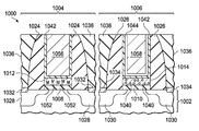
- NMOS gate sidewall spacers ( 1024 ) are formed on lateral surfaces of the NMOS dummy gate layer ( 1016 ), the NMOS gate work function metal layer ( 1012 ) and the NMOS gate dielectric layer ( 1008 ), typically by deposition of one or more conformal layers of silicon nitride and/or silicon oxide on a top and lateral surfaces of the NMOS gate layers and the top surface of the substrate ( 1002 ), followed by removal of the conformal layer material from the top surface of the NMOS hard mask ( 1020 ) and the top surface of the substrate ( 1002 ) by anisotropic etching methods, leaving the conformal layer material on the lateral surfaces of the NMOS dummy gate layer ( 1016 ), the NMOS gate work function metal layer ( 1012 ) and the NMOS gate dielectric layer ( 1008 ).
- the NMOS gate sidewall spacers ( 1024 ) are typically 10 to 50 nanometers thick.
- PMOS gate sidewall spacers ( 1026 ) are formed on lateral surfaces of the PMOS dummy gate layer ( 1018 ), the PMOS gate work function metal layer ( 1014 ) and the PMOS gate dielectric layer ( 1010 ). It is typical for a part of the PMOS gate sidewall spacers ( 1026 ) to be formed concurrently with the NMOS gate sidewall spacers ( 1024 ).
- N-type source and drain (NSD) regions ( 1028 ), including n-type lightly doped drain (NLDD) regions, are formed in the substrate ( 1002 ) adjacent to the NMOS gate dielectric layer ( 1008 ) by ion implanting n-type dopants such as phosphorus and arsenic into the substrate ( 1002 ).
- NLDD regions are formed by implanting n-type NLDD dopants adjacent to the NMOS gate dielectric layer ( 1008 ) prior to formation of the NMOS gate sidewall spacers ( 1024 ). Additional n-type NSD dopants are implanted after formation of the NMOS gate sidewall spacers ( 1024 ) and annealed to form the NSD regions ( 1028 ).
- p-type source and drain (PSD) regions ( 1030 ), including p-type lightly doped drain (PLDD) regions, are formed in the substrate ( 1002 ) adjacent to the PMOS gate dielectric layer ( 1010 ) by ion implanting p-type dopants such as boron and possibly gallium into the substrate ( 1002 ).
- PLDD regions are formed by implanting p-type PLDD dopants adjacent to the PMOS gate dielectric layer ( 1010 ) prior to formation of the PMOS gate sidewall spacers ( 1026 ). Additional p-type PSD dopants are implanted after formation of the PMOS gate sidewall spacers ( 1026 ) and annealed to form the PSD regions ( 1030 ).
- NSD metal silicide layers ( 1032 ) are formed on top surfaces of the NSD regions ( 1028 ) and PSD metal silicide layers ( 1034 ) are formed on top surfaces of the PSD regions ( 1030 ).
- the metal silicide layers ( 1032 , 1034 ) are formed on exposed silicon areas of the top surface of integrated circuit ( 1000 ), commonly by depositing a layer of metal, such as nickel, cobalt, or titanium, on a top surface of the IC ( 1000 ), heating the IC ( 1000 ) to react a portion of the metal with exposed silicon in active areas of the IC ( 1000 ), and selectively removing unreacted metal from the IC ( 1000 ) surface, commonly by exposing the IC ( 1000 ) to wet etchants including a mixture of an acid and hydrogen peroxide.
- the NMOS hard mask ( 1020 ) desirably blocks formation of metal silicide on the top surface of the NMOS dummy gate layer ( 1016 ), and the PMOS hard mask ( 1022 ) desirably blocks formation of metal silicide on the top surface of the PMOS dummy gate layer ( 1018 ). It is desirable to block formation of metal silicide on the top surfaces of the NMOS dummy gate layer ( 1016 ) and the PMOS dummy gate layer ( 1018 ) so as to improve etch characteristics of the dummy gate layers ( 1016 , 1020 ) during a subsequent dummy gate removal process.
- a conformal fill oxide layer ( 1036 ) is formed on an existing top surface of the integrated circuit ( 1000 ).
- the fill oxide layer ( 1036 ) is composed substantially of silicon dioxide, formed by thermal decomposition of tetraethyl orthosilicate, also known as tetraethoxysilane or TEOS, by thermal curing of methylsilsesquioxane (MSQ), by a high density plasma (HDP) process, by an ozone based thermal chemical vapor deposition (CVD) process, also known as a high aspect ratio process (HARP), by a low pressure chemical vapor deposition (LPCVD) process or by an atmospheric pressure chemical vapor deposition (APCVD) process.
- tetraethyl orthosilicate also known as tetraethoxysilane or TEOS
- MSQ methylsilsesquioxane
- HDP high density plasma
- CVD ozone based thermal chemical vapor deposition
- HTP high aspect ratio process
- the fill oxide layer ( 1036 ) is removed from top surfaces of the NMOS hard mask ( 1020 ) and the PMOS hard mask ( 1022 ) by a selective removal process such as an oxide CMP process.
- the NMOS hard mask ( 1020 ) and the PMOS hard mask ( 1022 ) desirably provide stop layers for the CMP process.
- FIG. 1D depicts the integrated circuit ( 1000 ) after an etchback process ( 1038 ) which removes the NMOS hard mask ( 1020 ) and the PMOS hard mask ( 1022 ), and removes material from top surfaces of the NMOS gate sidewall spacers ( 1024 ), the PMOS gate sidewall spacers ( 1026 ) and the fill oxide layer ( 1036 ).
- the etchback process ( 1038 ) provides substantially equal etch rates of the NMOS hard mask ( 1020 ), the PMOS hard mask ( 1022 ), the NMOS gate sidewall spacers ( 1024 ), the PMOS gate sidewall spacers ( 1026 ) and the fill oxide layer ( 1036 ).
- the etchback process ( 1038 ) may include an RIE step using fluorine containing etchants and possibly oxygen radicals and/or ions.
- FIG. 1E depicts the integrated circuit ( 1000 ) after a dummy gate removal process.
- the integrated circuit ( 1000 ) is exposed to wet etchants which include aqueous ammonium hydroxide (NH 4 OH) at a concentration between 0.5 and 5 percent, at a temperature between 25° C. and 50° C., for 20 to 150 seconds.
- the integrated circuit ( 1000 ) is exposed to wet etchants which include an aqueous mixture of NH 4 OH and tetra-methyl ammonium hydroxide (TMAH).
- TMAH tetra-methyl ammonium hydroxide
- the integrated circuit ( 1000 ) is exposed to wet etchants which include choline.
- the NMOS dummy gate layer material and the PMOS dummy gate layer material is removed from the NMOS region ( 1004 ) and the PMOS region ( 1006 ) while providing an etch selectivity to the NMOS gate work function metal layer ( 1012 ) and the PMOS gate work function metal layer ( 1014 ) of more than 100:1.
- FIG. 1F depicts the integrated circuit ( 1000 ) during a low temperature oxidation process.
- Oxygen atoms ( 1040 ) are provided by the low temperature oxidation process to an existing top surface of the integrated circuit ( 1000 ), and diffuse in to the NMOS gate work function metal layer ( 1012 ) and the PMOS gate work function metal layer ( 1014 ).
- the oxygen atoms ( 1040 ) in the gate work function metal layers ( 1012 , 1014 ) may have a distribution of at least 1 ⁇ 10 15 atoms/cm 2 within 1 nanometer of the top surfaces of the NMOS gate dielectric layer ( 1008 ) and the PMOS gate dielectric layer ( 1010 ).
- the oxygen atoms ( 1040 ) in the gate work function metal layers ( 1012 , 1014 ) may have an average concentration between 1 ⁇ 10 18 atoms/cm 3 and 1 ⁇ 10 21 atoms/cm 3 .
- the oxygen atoms ( 1040 ) in the gate work function metal layers ( 1012 , 1014 ) increase the effective work functions of the gate work function metal layers ( 1012 , 1014 ) to above 4.85 eV.
- the integrated circuit ( 1000 ) may be exposed to a steam ambient between 300° C. and 600° C. for 10 seconds to 30 minutes, as described in U.S. Patent Provisional Application 61/116,892, filed Nov. 21, 2008 hereby incorporated by reference.
- the integrated circuit may be exposed to a steam ambient between 900° C. and 1100° C. for less than 1 second, as described in the aforementioned U.S. Patent Provisional Application.
- the integrated circuit ( 1000 ) may be exposed to a plasma containing oxygen and hydrogen at a temperature up to 500° C., as described in the aforementioned US Patent Provisional Application.
- the integrated circuit may be exposed to a plasma containing oxygen, and subsequently exposed to a plasma containing hydrogen, as described in the aforementioned US Patent Provisional Application.
- the gate work function metal layers ( 1012 , 1014 ) may be anodized at a temperature up to 100° C., as described in the aforementioned US Patent Provisional Application.
- the integrated circuit ( 1000 ) may be exposed to a dry ambient containing an oxidizing component, such as oxygen (O 2 ), ozone (O 3 ), nitric oxide (NO), nitrous oxide (NO 2 ), or any combination of these gases.
- the ambient may also include inert gases such as nitrogen or argon.
- the integrated circuit ( 1000 ) may be heated to 300° C. to 700° C. during exposure to the dry ambient.
- the integrated circuit ( 1000 ) may be exposed to H 2 O containing dissolved ozone.
- FIG. 1G depicts the integrated circuit ( 1000 ) after formation of an etch stop layer and an oxygen diffusion barrier layer.
- a thin etch stop layer ( 1042 ) is formed on an existing top surface of the integrated circuit ( 1000 ) including the top surfaces of the NMOS gate work function metal layer ( 1012 ) and the PMOS gate work function metal layer ( 1014 ).
- the etch stop layer ( 1042 ) is between 2 and 10 nanometers thick over the NMOS gate work function metal layer ( 1012 ) and the PMOS gate work function metal layer ( 1014 ), and is formed of a metallic material which allows oxygen to diffuse across the etch stop layer ( 1042 ) during a subsequent getter anneal process step, and provides an etch stop capability during a subsequent oxygen diffusion barrier etch process step, such as TaN, tungsten nitride (WN), titanium carbide (TiC), TaC, or tungsten carbide (WC).
- the etch stop layer ( 1042 ) may be formed by ALD, CVD, PVD, MOCVD or other suitable deposition method.
- An oxygen diffusion barrier layer ( 1044 ) is formed on a top surface of the etch stop layer ( 1042 ).
- the oxygen diffusion barrier layer ( 1044 ) is greater than 10 nanometers thick over the NMOS gate work function metal layer ( 1012 ) and the PMOS gate work function metal layer ( 1014 ), and is formed of a metallic material which blocks oxygen diffusion during the subsequent getter anneal process step, and has a high etch rate selectivity to the etch stop layer ( 1042 ) during the subsequent oxygen diffusion barrier etch process step, such as TiN.
- the oxygen diffusion barrier layer ( 1044 ) may be formed by ALD, CVD, PVD, MOCVD or other suitable deposition method.
- FIG. 1H depicts the integrated circuit ( 1000 ) during a process step to remove the oxygen diffusion barrier layer ( 1044 ) in the NMOS region ( 1004 ).
- An oxygen diffusion barrier photoresist pattern ( 1046 ) is formed on a top surface of the oxygen diffusion barrier layer ( 1044 ) in the PMOS region ( 1006 ).
- An oxygen diffusion barrier etch process ( 1048 ) is performed which removes substantially all the oxygen diffusion barrier layer ( 1044 ) in the NMOS region ( 1004 ) from the top surface of the etch stop layer ( 1042 ) in direct contact with the NMOS gate work function metal layer ( 1012 ).
- the oxygen diffusion barrier etch process ( 1048 ) may be an RIE process using chlorine etchants and possibly fluorine etchants.
- the oxygen diffusion barrier photoresist pattern ( 1046 ) is removed from the top surface of the oxygen diffusion barrier layer ( 1044 ), for example by exposing the integrated circuit ( 1000 ) to an oxygen containing plasma, followed by a wet cleanup to remove any organic residue from the top surface of the oxygen diffusion barrier layer ( 1044 ).
- FIG. 1I depicts the integrated circuit ( 1000 ) after formation of a oxygen getter layer ( 1050 ) on the top surface of the etch stop layer ( 1042 ) over the NMOS gate work function metal layer ( 1012 ) and on the top surface of the oxygen diffusion barrier layer ( 1044 ) over the PMOS gate work function metal layer ( 1014 ).
- the oxygen getter layer ( 1050 ) may be formed on an existing top surface of the integrated circuit ( 1000 ).
- the oxygen getter layer ( 1050 ) may include titanium, hafnium, zirconium, tantalum, aluminum, cerium, lanthanum, or other metal capable of gettering oxygen atoms from the NMOS gate work function metal layer ( 1012 ) during a subsequent getter anneal process step.
- the oxygen getter layer ( 1050 ) may be formed by ALD, CVD, PVD, MOCVD or other suitable deposition method.
- FIG. 1J depicts the integrated circuit ( 1000 ) during the getter anneal process step, in which the integrated circuit ( 1000 ) is heated to cause the oxygen atoms ( 1040 ) to diffuse from the NMOS gate work function metal layer ( 1012 ) through the etch stop layer ( 1042 ) into the oxygen getter layer ( 1050 ) in the NMOS region ( 1004 ).
- metal atoms ( 1052 ) diffuse from the oxygen getter layer ( 1050 ) in the NMOS region ( 1004 ) through the etch stop layer ( 1042 ) into NMOS gate work function metal layer ( 1012 ).
- the effect of the getter anneal process is to reduce the effective work function of the NMOS gate work function metal layer ( 1012 ) to a value below 4.25 eV.
- the oxygen atoms ( 1040 ) in the NMOS gate work function metal layer ( 1012 ) have a distribution of less than 1 ⁇ 10 13 atoms/cm 2 within 1 nanometer of the top surface of the NMOS gate dielectric layer ( 1008 ).
- Metal atoms ( 1052 ) from the oxygen getter layer ( 1050 ) have a distribution of at least 1 ⁇ 10 13 atoms/cm 2 within 1 nanometer of the top surface of the NMOS gate dielectric layer ( 1008 ).
- Oxygen gettering in the PMOS region ( 1006 ) is blocked by the oxygen diffusion barrier layer ( 1044 ). Less than 10 percent of the oxygen atoms ( 1040 ) in the PMOS gate work function metal layer ( 1014 ) are removed during the getter anneal process, so that the effective work function of the PMOS gate work function metal layer ( 1014 ) remains above 4.85 eV.
- the getter anneal process is performed at less than 600° C. to avoid unwanted reactions in the silicide layers ( 1032 , 1034 ).
- the getter anneal process is performed in an inert ambient such as nitrogen or argon.
- the getter anneal process is performed at an ambient pressure below 1 millitorr.
- FIG. 1K depicts the integrated circuit ( 1000 ) after removing the oxygen getter layer.
- An oxygen getter etch process is performed, which may include immersion in an aqueous solution of a mixture of hydrogen peroxide and an alkaline etchant such as NH 4 OH. All or part of the oxygen diffusion barrier layer ( 1044 ) may be removed from the PMOS region ( 1006 ). All or part of the etch stop layer ( 1042 ) in direct contact with the NMOS gate work function metal layer ( 1012 ) may be removed during the oxygen getter etch process. Similarly, all or part of the etch stop layer ( 1042 ) in direct contact with the PMOS gate work function metal layer ( 1014 ) may be removed during the oxygen getter etch process.
- FIG. 1L depicts the integrated circuit ( 1000 ) after formation of a metal fill gate layer ( 1054 ) over the NMOS gate work function metal layer ( 1012 ) and the PMOS gate work function metal layer ( 1014 ).
- the metal fill gate layer ( 1054 ) may be formed on an existing top surface of the integrated circuit ( 1000 ).
- the metal fill gate layer ( 1054 ) may be aluminum, tungsten, or any metal with a suitably low electrical resistivity.
- the metal fill gate layer ( 1054 ) may be formed by ALD, CVD, PVD, MOCVD or other suitable deposition method.
- FIG. 1M depicts the integrated circuit ( 1000 ) after a planarizing process which removes the metal fill gate layer, the oxygen diffusion barrier layer ( 1044 ) if present, and the etch stop layer ( 1042 ) if present, from the top surface of the fill oxide layer ( 1036 ).
- Material from the metal fill gate layer is left over the NMOS gate work function metal layer ( 1012 ) to form an NMOS metal fill gate ( 1056 ) and is left over the PMOS gate work function metal layer ( 1014 )) to form a PMOS metal fill gate ( 1058 ).
- the planarizing process may be a CMP process, an isotropic chemical or physical etch process, or a combinations thereof.
- Formation of the integrated circuit ( 1000 ) is continued using known processes.
Abstract
A process is disclosed of forming metal replacement gates for NMOS and PMOS transistors with oxygen in the PMOS metal gates and metal atom enrichment in the NMOS gates such that the PMOS gates have effective work functions above 4.85 eV and the NMOS gates have effective work functions below 4.25 eV. Metal work function layers in both the NMOS and PMOS gates are oxidized to increase their effective work functions to the desired PMOS range. An oxygen diffusion blocking layer is formed over the PMOS gate and an oxygen getter is formed over the NMOS gates. A getter anneal extracts the oxygen from the NMOS work function layers and adds metal atom enrichment to the NMOS work function layers, reducing their effective work functions to the desired NMOS range. Processes and materials for the metal work function layers, the oxidation process and oxygen gettering are disclosed.
Description
The following patent application is related and hereby incorporated by reference: U.S. Patent Provisional Application 61/116,892, filed Nov. 21, 2008).
This invention relates to the field of integrated circuits. More particularly, this invention relates to replacement metal gates of MOS transistors in integrated circuits.
N-channel metal oxide semiconductor (NMOS) and p-channel metal oxide semiconductor (PMOS) transistors in advanced integrated circuits frequently have replacement metal gates to improve on-state current densities. Attaining desired effective work functions of the metal gates in both NMOS and PMOS transistors without significantly increasing fabrication cost and complexity has been problematic.
The instant invention provides a process for forming an integrated circuit which includes NMOS and PMOS transistors with metal replacement gates. The process forms gate work function metal layers in the PMOS transistors with effective work functions above 4.85 eV and gate work function metal layers in the NMOS transistors with effective work functions below 4.25 eV.
Work function metal layers with effective work functions approximately at mid-gap are formed in both the NMOS and PMOS gates. The work function metal layers are oxidized to increase their effective work functions to the desired PMOS range. Various oxidation processes suitable for this step are disclosed.
An oxygen diffusion blocking layer is formed over the PMOS gate and an oxygen getter is formed over both gates. Materials for the oxygen diffusion blocking layer and the getter are disclosed. A getter anneal extracts the oxygen from the NMOS work function layers into the getter material and adds metal atoms from the getter into the NMOS work function layers, reducing their effective work functions to the desired NMOS range.
The getter is removed and a metal replacement gate material is formed in both NMOS and PMOS gates.
The present invention is described with reference to the attached figures, wherein like reference numerals are used throughout the figures to designate similar or equivalent elements. The figures are not drawn to scale and they are provided merely to illustrate the invention. Several aspects of the invention are described below with reference to example applications for illustration. It should be understood that numerous specific details, relationships, and methods are set forth to provide a full understanding of the invention. One skilled in the relevant art, however, will readily recognize that the invention can be practiced without one or more of the specific details or with other methods. In other instances, well-known structures or operations are not shown in detail to avoid obscuring the invention. The present invention is not limited by the illustrated ordering of acts or events, as some acts may occur in different orders and/or concurrently with other acts or events. Furthermore, not all illustrated acts or events are required to implement a methodology in accordance with the present invention.
For the purposes of this disclosure, the term “eV” is understood to mean the unit of energy known as electron-volt. One eV is substantially equal to 1.602×10⁻¹⁹ joules. The term “meV” is understood to mean milli-electron volts. One meV is substantially equal to 1.602×10⁻²² joules.
For the purposes of this disclosure, the term “MOS transistor” will be understood to mean metal oxide semiconductor transistor.
For the purposes of this disclosure, the term “work function” will be understood to mean a potential energy difference, measured in eV, between an electron at the Fermi level in a material, to which the work function is being referenced, and an electron in a vacuum adjacent to the material. For example, intrinsic silicon has a work function of approximately 4.6 eV at room temperature. N-type silicon with a doping density between 3×1017 cm−3 and 3×1018 cm−3 has a work function of approximately 4.1 eV at room temperature. P-type silicon with a doping density between 3×1017 cm−3 and 3×1018 cm−3 has a work function of approximately 5.1 eV at room temperature. The term “effective work function” will be understood to mean a calculated potential energy of an electron in a gate in an MOS transistor which is consistent with an observed flat-band potential and all substrate and gate interface charge effects.
For the purposes of this disclosure, the term “getter” will be understood to refer to a material which has a capability of absorbing an element such as oxygen from a region surrounding the getter material. Similarly, the term “gettering” will be understood to mean the act of absorbing an element into a getter material.
Chemical formulas such as SiON of a material in this disclosure are understood to list elements of which the material is substantially composed, but no stoichiometric relationships between the elements are implied or may be assumed, unless numerical subscripts are included in the chemical formulas.
The instant invention provides a process for forming an integrated circuit which includes NMOS and PMOS transistors with metal replacement gates. The process forms gate work function metal layers in the PMOS transistors with effective work functions above 4.85 eV and gate work function metal layers in the NMOS transistors with effective work functions below 4.25 eV.
A PMOS gate dielectric layer (1010) is formed on a top surface of the substrate (1002) in the PMOS region (1006). The PMOS gate dielectric layer (1010) is typically between 1 and 4 nanometers thick, and includes some or all of the same materials in the NMOS gate dielectric layer (1008). A thicker PMOS gate dielectric layer (1010) may be formed in PMOS transistors operating above 2.5 volts. All or part of the PMOS gate dielectric layer (1010) is typically formed concurrently with the NMOS gate dielectric layer (1008).
An NMOS gate work function metal layer (1012) is formed on a top surface of the NMOS gate dielectric layer (1008). The NMOS gate work function metal layer (1012) may be titanium nitride (TiN), tantalum nitride (TaN), tantalum carbide (TaC), or other metal with an effective work function between 4.5 and 4.7 eV. The NMOS gate work function metal layer (1012) may be between 1 and 10 nanometers thick, and may be formed by physical vapor deposition (PVD), chemical vapor deposition (CVD), metal-organic chemical vapor deposition (MOCVD), ALD, or other process appropriate for deposition of thin metal films. A PMOS gate work function metal layer (1014) is formed on a top surface of the PMOS gate dielectric layer (1010) of similar materials and properties as the NMOS gate work function metal layer (1012). In one embodiment, the PMOS gate work function metal layer (1014) may be formed concurrently with the NMOS gate work function metal layer (1012).
An NMOS dummy gate layer (1016) is formed on a top surface of the NMOS gate work function metal layer (1012). The NMOS dummy gate layer (1016) may be polycrystalline silicon, commonly known as polysilicon, or other material such as silicon germanium which has a high etch selectivity to the NMOS gate work function metal layer (1012) during a subsequent wet etch process. In one embodiment, the NMOS dummy gate layer (1016) is between 40 and 80 nanometers thick. In another embodiment, the thickness of the NMOS dummy gate layer (1016) is between two and three times a width of an NMOS gate to be formed in the NMOS region (1004). The NMOS dummy gate layer (1016) may be formed by plasma enhanced chemical vapor deposition (PECVD) or other deposition process appropriate for forming thin films of dummy gate material. In an alternate embodiment, the NMOS dummy gate layer (1016) may be doped with phosphorus to improve etch selectivity to the NMOS gate work function metal layer (1012) during the subsequent wet etch process.
A PMOS dummy gate layer (1018) is formed on a top surface of the PMOS gate work function metal layer (1014) of similar materials and properties as the NMOS dummy gate layer (1016). In one embodiment, the PMOS dummy gate layer (1018) may be formed concurrently with the NMOS dummy gate layer (1016).
An NMOS hard mask (1020) is formed on a top surface of the NMOS dummy gate layer (1016). The NMOS hard mask (1020) may include one or more layers of silicon nitride (SiN), silicon oxy-nitride (SiON), silicon carbide (SiC), silicon oxy-carbide (SiOC), silicon oxy-nitride-carbide (SiCON), or other dielectric material appropriate for blocking silicidation of the top surface of the NMOS dummy gate layer (1016) during a subsequent silicidation process, and appropriate for providing a stop layer for a subsequent chemical mechanical polish (CMP) process. The NMOS hard mask (1020) may be formed by PVD, CVD, PECVD, MOCVD or other deposition process. In one embodiment, the NMOS hard mask (1020) may be between 20 and 40 nanometers thick.
A PMOS hard mask (1022) is formed on a top surface of the PMOS dummy gate layer (1018) of similar materials and properties as the NMOS hard mask (1020). In one embodiment, the PMOS hard mask (1022) may be formed concurrently with the NMOS hard mask (1020).
Referring to FIG. 1B , unwanted material from the NMOS hard mask (1020), the NMOS dummy gate layer (1016), the NMOS gate work function metal layer (1012) and the NMOS gate dielectric layer (1008) is removed during a gate etch process. Similarly, unwanted material from the PMOS hard mask (1022), the PMOS dummy gate layer (1018), the PMOS gate work function metal layer (1014) and the PMOS gate dielectric layer (1010) is removed during the gate etch process. A gate photoresist pattern, not shown in FIG. 1B for clarity, is formed on top surfaces of the NMOS hard mask (1020) and the PMOS hard mask (1022). The gate etch process includes reactive ion etch (RIE) process steps which provide fluorine containing etchants and possibly chlorine containing etchants from a plasma to a top surface of the integrated circuit (1000). The photoresist pattern blocks the etchants from areas of the NMOS region (1004) and PMOS region (1006) defined for an NMOS gate and a PMOS gate.
NMOS gate sidewall spacers (1024) are formed on lateral surfaces of the NMOS dummy gate layer (1016), the NMOS gate work function metal layer (1012) and the NMOS gate dielectric layer (1008), typically by deposition of one or more conformal layers of silicon nitride and/or silicon oxide on a top and lateral surfaces of the NMOS gate layers and the top surface of the substrate (1002), followed by removal of the conformal layer material from the top surface of the NMOS hard mask (1020) and the top surface of the substrate (1002) by anisotropic etching methods, leaving the conformal layer material on the lateral surfaces of the NMOS dummy gate layer (1016), the NMOS gate work function metal layer (1012) and the NMOS gate dielectric layer (1008). The NMOS gate sidewall spacers (1024) are typically 10 to 50 nanometers thick. Similarly, PMOS gate sidewall spacers (1026) are formed on lateral surfaces of the PMOS dummy gate layer (1018), the PMOS gate work function metal layer (1014) and the PMOS gate dielectric layer (1010). It is typical for a part of the PMOS gate sidewall spacers (1026) to be formed concurrently with the NMOS gate sidewall spacers (1024).
N-type source and drain (NSD) regions (1028), including n-type lightly doped drain (NLDD) regions, are formed in the substrate (1002) adjacent to the NMOS gate dielectric layer (1008) by ion implanting n-type dopants such as phosphorus and arsenic into the substrate (1002). NLDD regions are formed by implanting n-type NLDD dopants adjacent to the NMOS gate dielectric layer (1008) prior to formation of the NMOS gate sidewall spacers (1024). Additional n-type NSD dopants are implanted after formation of the NMOS gate sidewall spacers (1024) and annealed to form the NSD regions (1028). Similarly, p-type source and drain (PSD) regions (1030), including p-type lightly doped drain (PLDD) regions, are formed in the substrate (1002) adjacent to the PMOS gate dielectric layer (1010) by ion implanting p-type dopants such as boron and possibly gallium into the substrate (1002). PLDD regions are formed by implanting p-type PLDD dopants adjacent to the PMOS gate dielectric layer (1010) prior to formation of the PMOS gate sidewall spacers (1026). Additional p-type PSD dopants are implanted after formation of the PMOS gate sidewall spacers (1026) and annealed to form the PSD regions (1030).
NSD metal silicide layers (1032) are formed on top surfaces of the NSD regions (1028) and PSD metal silicide layers (1034) are formed on top surfaces of the PSD regions (1030). The metal silicide layers (1032, 1034) are formed on exposed silicon areas of the top surface of integrated circuit (1000), commonly by depositing a layer of metal, such as nickel, cobalt, or titanium, on a top surface of the IC (1000), heating the IC (1000) to react a portion of the metal with exposed silicon in active areas of the IC (1000), and selectively removing unreacted metal from the IC (1000) surface, commonly by exposing the IC (1000) to wet etchants including a mixture of an acid and hydrogen peroxide. The NMOS hard mask (1020) desirably blocks formation of metal silicide on the top surface of the NMOS dummy gate layer (1016), and the PMOS hard mask (1022) desirably blocks formation of metal silicide on the top surface of the PMOS dummy gate layer (1018). It is desirable to block formation of metal silicide on the top surfaces of the NMOS dummy gate layer (1016) and the PMOS dummy gate layer (1018) so as to improve etch characteristics of the dummy gate layers (1016, 1020) during a subsequent dummy gate removal process.
Referring to FIG. 1C , a conformal fill oxide layer (1036) is formed on an existing top surface of the integrated circuit (1000). In one embodiment, the fill oxide layer (1036) is composed substantially of silicon dioxide, formed by thermal decomposition of tetraethyl orthosilicate, also known as tetraethoxysilane or TEOS, by thermal curing of methylsilsesquioxane (MSQ), by a high density plasma (HDP) process, by an ozone based thermal chemical vapor deposition (CVD) process, also known as a high aspect ratio process (HARP), by a low pressure chemical vapor deposition (LPCVD) process or by an atmospheric pressure chemical vapor deposition (APCVD) process. The fill oxide layer (1036) is removed from top surfaces of the NMOS hard mask (1020) and the PMOS hard mask (1022) by a selective removal process such as an oxide CMP process. The NMOS hard mask (1020) and the PMOS hard mask (1022) desirably provide stop layers for the CMP process.
In a first embodiment of the low temperature oxidation process, the integrated circuit (1000) may be exposed to a steam ambient between 300° C. and 600° C. for 10 seconds to 30 minutes, as described in U.S. Patent Provisional Application 61/116,892, filed Nov. 21, 2008 hereby incorporated by reference. In an alternate embodiment, the integrated circuit may be exposed to a steam ambient between 900° C. and 1100° C. for less than 1 second, as described in the aforementioned U.S. Patent Provisional Application.
In a second embodiment of the low temperature oxidation process, the integrated circuit (1000) may be exposed to a plasma containing oxygen and hydrogen at a temperature up to 500° C., as described in the aforementioned US Patent Provisional Application. In an alternate embodiment, the integrated circuit may be exposed to a plasma containing oxygen, and subsequently exposed to a plasma containing hydrogen, as described in the aforementioned US Patent Provisional Application.
In a third embodiment of the low temperature oxidation process, the gate work function metal layers (1012, 1014) may be anodized at a temperature up to 100° C., as described in the aforementioned US Patent Provisional Application.
In a fourth embodiment of the low temperature oxidation process, the integrated circuit (1000) may be exposed to a dry ambient containing an oxidizing component, such as oxygen (O2), ozone (O3), nitric oxide (NO), nitrous oxide (NO2), or any combination of these gases. The ambient may also include inert gases such as nitrogen or argon. The integrated circuit (1000) may be heated to 300° C. to 700° C. during exposure to the dry ambient.
In a fifth embodiment of the low temperature oxidation process, the integrated circuit (1000) may be exposed to H2O containing dissolved ozone.
Oxygen gettering in the PMOS region (1006) is blocked by the oxygen diffusion barrier layer (1044). Less than 10 percent of the oxygen atoms (1040) in the PMOS gate work function metal layer (1014) are removed during the getter anneal process, so that the effective work function of the PMOS gate work function metal layer (1014) remains above 4.85 eV.
The getter anneal process is performed at less than 600° C. to avoid unwanted reactions in the silicide layers (1032, 1034). In one embodiment, the getter anneal process is performed in an inert ambient such as nitrogen or argon. In an alternate embodiment, the getter anneal process is performed at an ambient pressure below 1 millitorr.
Formation of the integrated circuit (1000) is continued using known processes.
Claims (8)
1. An integrated circuit, comprising:
a substrate;
a PMOS transistor, said PMOS transistor further including:
a PMOS gate dielectric layer formed on a top surface of said substrate;
a PMOS gate work function metal layer formed on a top surface of said PMOS gate dielectric layer, wherein said PMOS gate work function metal layer includes oxygen such that an effective work function of said PMOS gate work function metal layer is above 4.85 eV;
a PMOS metal fill gate formed over and in electrical connection with said PMOS gate work function metal layer;
a PMOS etch stop layer between the PMOS gate work function metal layer and the PMOS metal fill gate; and
an oxygen diffusion barrier between the PMOS gate work function metal layer and the PMOS metal fill gate; and
an NMOS transistor, said NMOS transistor further including:
an NMOS gate dielectric layer formed on a top surface of said substrate;
an NMOS gate work function metal layer formed on a top surface of said NMOS gate dielectric layer, wherein said NMOS gate work function metal layer includes additional metal atoms relative to said PMOS gate work function metal layer such that an effective work function of said NMOS gate work function metal layer is below 4.25 eV;
an NMOS metal fill gate formed over and in electrical connection with said NMOS gate work function metal layer, the NMOS transistor not including the oxygen diffusion barrier; and
an NMOS etch stop layer between the NMOS gate work function layer and the NMOS metal fill gate.
2. The integrated circuit of claim 1 , wherein:
a composition of said PMOS gate dielectric layer and composition of said NMOS gate dielectric layer are each selected from the group consisting of:
SiOx,
Si3N4,
SiON,
Al2O3,
AlON,
HfO,
HfSiO,
HfSiON,
ZrO,
ZrSiO,
ZrSiON,
nitridated SiOx,
nitridated Al2O3,
nitridated HfO,
nitridated HfSiO,
nitridated ZrO,
nitridated ZrSiO, and
any combination thereof.
3. The integrated circuit of claim 1 , wherein:
said PMOS gate work function metal layer includes oxygen atoms such that said oxygen atoms have a distribution of at least 1×10¹⁵ atoms/cm2 within 1 nanometer of said top surface of said PMOS gate dielectric layer;
said NMOS gate work function metal layer includes oxygen atoms such that said oxygen atoms have a distribution less than 1×10¹³ oxygen atoms/cm2 within 1 nanometer of said top surface of said NMOS gate dielectric layer; and
said NMOS gate work function metal layer includes metal atoms from an oxygen getter layer such that said metal atoms have a distribution of at least 1×10¹³ atoms/cm2 within 1 nanometer of said top surface of said NMOS gate dielectric layer.
4. The integrated circuit of claim 1 , wherein:
said PMOS gate work function metal layer includes oxygen atoms such that said oxygen atoms have an average concentration between 1×10¹⁸ atoms/cm3 and 1×10²¹ atoms/cm3;
said NMOS gate work function metal layer includes oxygen atoms such that said oxygen atoms have an average concentration less than 1×10¹⁶ atoms/cm3; and
said NMOS gate work function metal layer includes metal atoms from an oxygen getter layer such that said metal atoms have a distribution of at least 1×10¹³ atoms/cm2 within 1 nanometer of said top surface of said NMOS gate dielectric layer.
5. The integrated circuit of claim 1 , in which:
said PMOS gate work function metal layer is between 1 and 10 nanometers thick; and
said NMOS gate work function metal layer is between 1 and 10 nanometers thick.
6. The integrated circuit of claim 1 , in which:
said PMOS gate work function metal layer and said NMOS gate work function metal layer each include a metal selected from the group consisting of:
TiN,
TaN, and
TaC.
7. An integrated circuit, comprising:
a substrate;
a PMOS transistor having a PMOS gate stack, wherein the PMOS gate stack includes a gate dielectric layer, a layer of TiN infused with oxygen atoms to achieve an effective work function above 4.85 eV, a layer of TaN, and a metal fill layer;
a NMOS transistor having a NMOS gate stack, wherein the NMOS gate stack includes the gate dielectric layer, a layer of TiN with additional metal atoms relative to the layer of TiN infused with oxygen atoms to achieve an effective work function below 4.25 eV, the layer of TaN and the metal fill layer.
8. An integrated circuit, comprising:
a substrate;
a PMOS transistor having a PMOS gate stack;
a NMOS transistor having a NMOS gate stack;
a gate dielectric layer located in said PMOS gate stack and said NMOS gate stack;
a PMOS gate work function metal layer located over said gate dielectric layer in said PMOS gate stack, wherein said PMOS gate work function metal layer includes oxygen such that an effective work function of said PMOS gate work function metal layer is above 4.85 eV;
an NMOS gate work function metal layer located over said gate dielectric layer in said NMOS gate stack, wherein said NMOS gate work function metal layer includes additional metal atoms such that an effective work function of said NMOS gate work function metal layer is below 4.25 eV;
a metal fill layer located in said PMOS gate stack and said NMOS gate stack;
an etch stop layer located in said PMOS gate stack between the PMOS gate work function layer and the metal fill layer and in said NMOS gate stack between the NMOS gate work function layer and the metal fill layer, said etch stop layer comprising a metallic material that allows oxygen to diffuse across the etch stop layer; and
an oxygen diffusion barrier located between the PMOS gate work function metal layer and the metal fill gate in the PMOS gate stack and not located in the NMOS gate stack, said oxygen diffusion barrier comprising a metallic material that blocks oxygen diffusion and has a high etch rate selectivity to the etch stop layer.
Priority Applications (3)
| Application Number | Priority Date | Filing Date | Title |
|---|---|---|---|
| US12/275,812 US8643113B2 (en) | 2008-11-21 | 2008-11-21 | Structure and method for metal gate stack oxygen concentration control using an oxygen diffusion barrier layer and a sacrificial oxygen gettering layer |
| US14/146,095 US9087918B2 (en) | 2008-11-21 | 2014-01-02 | Structure and method for metal gate stack oxygen concentration control using an oxygen diffusion barrier layer and a sacrificial oxygen gettering layer |
| US14/739,681 US9397009B2 (en) | 2008-11-21 | 2015-06-15 | Structure and method for metal gate stack oxygen concentration control using an oxygen diffusion barrier layer and a sacrificial oxygen gettering layer |
Applications Claiming Priority (1)
| Application Number | Priority Date | Filing Date | Title |
|---|---|---|---|
| US12/275,812 US8643113B2 (en) | 2008-11-21 | 2008-11-21 | Structure and method for metal gate stack oxygen concentration control using an oxygen diffusion barrier layer and a sacrificial oxygen gettering layer |
Related Child Applications (1)
| Application Number | Title | Priority Date | Filing Date |
|---|---|---|---|
| US14/146,095 Division US9087918B2 (en) | 2008-11-21 | 2014-01-02 | Structure and method for metal gate stack oxygen concentration control using an oxygen diffusion barrier layer and a sacrificial oxygen gettering layer |
Publications (2)
| Publication Number | Publication Date |
|---|---|
| US20100127336A1 US20100127336A1 (en) | 2010-05-27 |
| US8643113B2 true US8643113B2 (en) | 2014-02-04 |
Family
ID=42195443
Family Applications (3)
| Application Number | Title | Priority Date | Filing Date |
|---|---|---|---|
| US12/275,812 Active 2031-04-12 US8643113B2 (en) | 2008-11-21 | 2008-11-21 | Structure and method for metal gate stack oxygen concentration control using an oxygen diffusion barrier layer and a sacrificial oxygen gettering layer |
| US14/146,095 Active 2028-12-27 US9087918B2 (en) | 2008-11-21 | 2014-01-02 | Structure and method for metal gate stack oxygen concentration control using an oxygen diffusion barrier layer and a sacrificial oxygen gettering layer |
| US14/739,681 Active US9397009B2 (en) | 2008-11-21 | 2015-06-15 | Structure and method for metal gate stack oxygen concentration control using an oxygen diffusion barrier layer and a sacrificial oxygen gettering layer |
Family Applications After (2)
| Application Number | Title | Priority Date | Filing Date |
|---|---|---|---|
| US14/146,095 Active 2028-12-27 US9087918B2 (en) | 2008-11-21 | 2014-01-02 | Structure and method for metal gate stack oxygen concentration control using an oxygen diffusion barrier layer and a sacrificial oxygen gettering layer |
| US14/739,681 Active US9397009B2 (en) | 2008-11-21 | 2015-06-15 | Structure and method for metal gate stack oxygen concentration control using an oxygen diffusion barrier layer and a sacrificial oxygen gettering layer |
Country Status (1)
| Country | Link |
|---|---|
| US (3) | US8643113B2 (en) |
Cited By (7)
| Publication number | Priority date | Publication date | Assignee | Title |
|---|---|---|---|---|
| US20160042953A1 (en) * | 2008-11-21 | 2016-02-11 | Texas Instruments Incorporated | Methods to enhance effective work function of mid-gap metal by incorporating oxygen and hydrogen at a low thermal budget |
| US9496183B1 (en) | 2015-05-07 | 2016-11-15 | International Business Machines Corporation | Selective thickening of pFET dielectric |
| US20180166274A1 (en) * | 2016-12-12 | 2018-06-14 | Taiwan Semiconductor Manufacturing Co., Ltd. | Metal gate structure and manufacturing method thereof |
| US10868171B2 (en) * | 2019-02-26 | 2020-12-15 | Taiwan Semiconductor Manufacturing Co., Ltd. | Semiconductor device structure with gate dielectric layer and method for forming the same |
| US10971593B2 (en) | 2019-06-14 | 2021-04-06 | International Business Machines Corporation | Oxygen reservoir for low threshold voltage P-type MOSFET |
| US11133305B2 (en) | 2019-05-15 | 2021-09-28 | International Business Machines Corporation | Nanosheet P-type transistor with oxygen reservoir |
| US11791391B1 (en) | 2022-03-18 | 2023-10-17 | Micron Technology, Inc. | Inverters, and related memory devices and electronic systems |
Families Citing this family (64)
| Publication number | Priority date | Publication date | Assignee | Title |
|---|---|---|---|---|
| US8643113B2 (en) * | 2008-11-21 | 2014-02-04 | Texas Instruments Incorporated | Structure and method for metal gate stack oxygen concentration control using an oxygen diffusion barrier layer and a sacrificial oxygen gettering layer |
| DE102009006802B3 (en) * | 2009-01-30 | 2010-06-17 | Advanced Micro Devices, Inc., Sunnyvale | A method and semiconductor device with work function adjustment in a high ε gate electrode structure after transistor fabrication using lanthanum |
| US20100327364A1 (en) * | 2009-06-29 | 2010-12-30 | Toshiba America Electronic Components, Inc. | Semiconductor device with metal gate |
| US8294202B2 (en) * | 2009-07-08 | 2012-10-23 | Taiwan Semiconductor Manufacturing Company, Ltd. | Metal gate structure of a semiconductor device |
| US8617946B2 (en) * | 2009-11-11 | 2013-12-31 | Taiwan Semiconductor Manufacturing Company, Ltd. | Integrated circuits including metal gates and fabrication methods thereof |
| DE102009047307B4 (en) * | 2009-11-30 | 2012-10-31 | Globalfoundries Dresden Module One Limited Liability Company & Co. Kg | A method for increasing the stability of a high-k gate dielectric in a high-k gate stack by an oxygen-rich titanium nitride capping layer |
| US8536654B2 (en) * | 2010-01-13 | 2013-09-17 | Texas Instruments Incorporated | Structure and method for dual work function metal gate CMOS with selective capping |
| US8653602B2 (en) | 2010-09-11 | 2014-02-18 | International Business Machines Corporation | Transistor having replacement metal gate and process for fabricating the same |
| US9166020B2 (en) * | 2011-03-01 | 2015-10-20 | United Microelectronics Corp. | Metal gate structure and manufacturing method thereof |
| US8802524B2 (en) * | 2011-03-22 | 2014-08-12 | United Microelectronics Corp. | Method of manufacturing semiconductor device having metal gates |
| TWI562211B (en) * | 2011-04-01 | 2016-12-11 | United Microelectronics Corp | Semiconductor device having metal gate and fabricating method thereof |
| US9384962B2 (en) * | 2011-04-07 | 2016-07-05 | United Microelectronics Corp. | Oxygen treatment of replacement work-function metals in CMOS transistor gates |
| CN102737971B (en) * | 2011-04-15 | 2016-08-17 | 联华电子股份有限公司 | There is semiconductor element and its manufacture method of metal gates |
| US8530980B2 (en) | 2011-04-27 | 2013-09-10 | United Microelectronics Corp. | Gate stack structure with etch stop layer and manufacturing process thereof |
| US8673758B2 (en) * | 2011-06-16 | 2014-03-18 | United Microelectronics Corp. | Structure of metal gate and fabrication method thereof |
| US8404530B2 (en) * | 2011-07-07 | 2013-03-26 | International Business Machines Corporation | Replacement metal gate with a conductive metal oxynitride layer |
| US8551876B2 (en) * | 2011-08-18 | 2013-10-08 | United Microelectronics Corp. | Manufacturing method for semiconductor device having metal gate |
| US8440520B2 (en) | 2011-08-23 | 2013-05-14 | Tokyo Electron Limited | Diffused cap layers for modifying high-k gate dielectrics and interface layers |
| CN102956460B (en) * | 2011-08-26 | 2017-06-06 | 联华电子股份有限公司 | The preparation method of the semiconductor element with metal gates |
| US9076889B2 (en) * | 2011-09-26 | 2015-07-07 | Taiwan Semiconductor Manufacturing Company, Ltd. | Replacement gate semiconductor device |
| US8772149B2 (en) | 2011-10-19 | 2014-07-08 | International Business Machines Corporation | FinFET structure and method to adjust threshold voltage in a FinFET structure |
| US8691681B2 (en) * | 2012-01-04 | 2014-04-08 | United Microelectronics Corp. | Semiconductor device having a metal gate and fabricating method thereof |
| US8633118B2 (en) | 2012-02-01 | 2014-01-21 | Tokyo Electron Limited | Method of forming thin metal and semi-metal layers by thermal remote oxygen scavenging |
| CN103311281B (en) * | 2012-03-14 | 2016-03-30 | 中国科学院微电子研究所 | Semiconductor device and manufacture method thereof |
| US8865538B2 (en) | 2012-03-30 | 2014-10-21 | Tokyo Electron Limited | Method of integrating buried threshold voltage adjustment layers for CMOS processing |
| US8987080B2 (en) * | 2012-04-26 | 2015-03-24 | Applied Materials, Inc. | Methods for manufacturing metal gates |
| JP5960491B2 (en) * | 2012-04-27 | 2016-08-02 | キヤノンアネルバ株式会社 | Semiconductor device and manufacturing method thereof |
| KR101909091B1 (en) | 2012-05-11 | 2018-10-17 | 삼성전자 주식회사 | Semiconductor device and fabricating method thereof |
| US9105623B2 (en) * | 2012-05-25 | 2015-08-11 | United Microelectronics Corp. | Semiconductor device having metal gate and manufacturing method thereof |
| US20140015068A1 (en) * | 2012-07-16 | 2014-01-16 | Hong Yang | Gate Structure, Semiconductor Device and Methods for Forming the Same |
| CN103545189A (en) * | 2012-07-16 | 2014-01-29 | 中国科学院微电子研究所 | Gate structure, semiconductor device and forming method of both |
| US8659077B1 (en) | 2012-09-13 | 2014-02-25 | International Business Machines Corporation | Multi-layer work function metal replacement gate |
| KR20140047920A (en) | 2012-10-15 | 2014-04-23 | 삼성전자주식회사 | Semiconductor device and fabricating method thereof |
| US8865581B2 (en) | 2012-10-19 | 2014-10-21 | Tokyo Electron Limited | Hybrid gate last integration scheme for multi-layer high-k gate stacks |
| US8999831B2 (en) * | 2012-11-19 | 2015-04-07 | International Business Machines Corporation | Method to improve reliability of replacement gate device |
| CN103855014B (en) * | 2012-11-30 | 2017-10-20 | 中国科学院微电子研究所 | P-type MOSFET and its manufacture method |
| CN103915323B (en) * | 2013-01-08 | 2016-08-31 | 中芯国际集成电路制造(上海)有限公司 | The preparation method of transistor |
| US8889540B2 (en) * | 2013-02-27 | 2014-11-18 | International Business Machines Corporation | Stress memorization in RMG FinFets |
| US9929310B2 (en) * | 2013-03-14 | 2018-03-27 | Applied Materials, Inc. | Oxygen controlled PVD aluminum nitride buffer for gallium nitride-based optoelectronic and electronic devices |
| US9105720B2 (en) | 2013-09-11 | 2015-08-11 | United Microelectronics Corp. | Semiconductor device having metal gate and manufacturing method thereof |
| US20150076624A1 (en) * | 2013-09-19 | 2015-03-19 | GlobalFoundries, Inc. | Integrated circuits having smooth metal gates and methods for fabricating same |
| US9564332B2 (en) * | 2013-09-26 | 2017-02-07 | Taiwan Semiconductor Manufacturing Co., Ltd. | Mechanism for forming metal gate structure |
| KR102084657B1 (en) * | 2013-11-04 | 2020-03-04 | 에스케이하이닉스 주식회사 | Method and gate ructure for threshold voltage modulation in transistors |
| KR102155511B1 (en) | 2013-12-27 | 2020-09-15 | 삼성전자 주식회사 | Semiconductor package and method for fabricating the same |
| CN104752176B (en) * | 2013-12-27 | 2017-12-29 | 中芯国际集成电路制造(上海)有限公司 | The forming method of metal gates |
| US9070785B1 (en) * | 2013-12-31 | 2015-06-30 | Texas Instruments Incorporated | High-k / metal gate CMOS transistors with TiN gates |
| US9147683B2 (en) * | 2014-02-18 | 2015-09-29 | International Business Machines Corporation | CMOS transistors including gate spacers of the same thickness |
| US10134732B2 (en) * | 2014-04-07 | 2018-11-20 | International Business Machines Corporation | Reduction of negative bias temperature instability |
| US9466492B2 (en) | 2014-05-02 | 2016-10-11 | International Business Machines Corporation | Method of lateral oxidation of NFET and PFET high-K gate stacks |
| US9190272B1 (en) | 2014-07-15 | 2015-11-17 | Samsung Electronics Co., Ltd. | Semiconductor device and method of fabricating the same |
| US10134871B2 (en) * | 2014-12-23 | 2018-11-20 | Taiwan Semiconductor Manufacturing Company, Ltd. | Doping of high-K dielectric oxide by wet chemical treatment |
| US9570578B2 (en) * | 2015-02-11 | 2017-02-14 | United Microelectronics Corp. | Gate and gate forming process |
| CN106409830B (en) | 2015-07-27 | 2020-05-05 | 联华电子股份有限公司 | Semiconductor element with metal grid and manufacturing method thereof |
| US9859392B2 (en) * | 2015-09-21 | 2018-01-02 | Samsung Electronics Co., Ltd. | Integrated circuit device and method of manufacturing the same |
| US9871114B2 (en) * | 2015-09-30 | 2018-01-16 | Taiwan Semiconductor Manufacturing Company, Ltd. | Metal gate scheme for device and methods of forming |
| US9583486B1 (en) * | 2015-11-19 | 2017-02-28 | International Business Machines Corporation | Stable work function for narrow-pitch devices |
| TWI713117B (en) * | 2017-01-05 | 2020-12-11 | 聯華電子股份有限公司 | Method for fabricating metal gate structure |
| CN108933083B (en) * | 2017-05-22 | 2020-09-08 | 中芯国际集成电路制造(上海)有限公司 | Semiconductor structure and forming method thereof |
| US11114347B2 (en) * | 2017-06-30 | 2021-09-07 | Taiwan Semiconductor Manufacturing Co., Ltd. | Self-protective layer formed on high-k dielectric layers with different materials |
| CN109545784A (en) | 2017-09-22 | 2019-03-29 | 联华电子股份有限公司 | Semiconductor element and preparation method thereof |
| US11302827B2 (en) * | 2020-01-23 | 2022-04-12 | Nanya Technology Corp. | Semiconductor device with sidewall oxidized dielectric and method for fabricating the same |
| US11380536B2 (en) | 2020-05-05 | 2022-07-05 | Applied Materials, Inc. | Multi-step pre-clean for selective metal gap fill |
| US11694958B2 (en) | 2020-06-03 | 2023-07-04 | International Business Machines Corporation | Layout design for threshold voltage tuning |
| CN111785621A (en) * | 2020-07-27 | 2020-10-16 | 上海华力集成电路制造有限公司 | Process method for inhibiting metal gate height asymmetry |
Citations (3)
| Publication number | Priority date | Publication date | Assignee | Title |
|---|---|---|---|---|
| US20080017930A1 (en) * | 2005-02-22 | 2008-01-24 | Samsung Electronics Co., Ltd. | Dual work function metal gate structure and related method of manufacture |
| US20080290416A1 (en) * | 2007-05-21 | 2008-11-27 | Taiwan Semiconductor Manufacturing Co., Ltd. | High-k metal gate devices and methods for making the same |
| US7646067B2 (en) * | 2006-08-21 | 2010-01-12 | Samsung Electronics Co., Ltd. | Complementary metal-oxide-semiconductor transistor including multiple gate conductive layers and method of manufacturing the same |
Family Cites Families (1)
| Publication number | Priority date | Publication date | Assignee | Title |
|---|---|---|---|---|
| US8643113B2 (en) * | 2008-11-21 | 2014-02-04 | Texas Instruments Incorporated | Structure and method for metal gate stack oxygen concentration control using an oxygen diffusion barrier layer and a sacrificial oxygen gettering layer |
-
2008
- 2008-11-21 US US12/275,812 patent/US8643113B2/en active Active
-
2014
- 2014-01-02 US US14/146,095 patent/US9087918B2/en active Active
-
2015
- 2015-06-15 US US14/739,681 patent/US9397009B2/en active Active
Patent Citations (3)
| Publication number | Priority date | Publication date | Assignee | Title |
|---|---|---|---|---|
| US20080017930A1 (en) * | 2005-02-22 | 2008-01-24 | Samsung Electronics Co., Ltd. | Dual work function metal gate structure and related method of manufacture |
| US7646067B2 (en) * | 2006-08-21 | 2010-01-12 | Samsung Electronics Co., Ltd. | Complementary metal-oxide-semiconductor transistor including multiple gate conductive layers and method of manufacturing the same |
| US20080290416A1 (en) * | 2007-05-21 | 2008-11-27 | Taiwan Semiconductor Manufacturing Co., Ltd. | High-k metal gate devices and methods for making the same |
Cited By (13)
| Publication number | Priority date | Publication date | Assignee | Title |
|---|---|---|---|---|
| US20160042953A1 (en) * | 2008-11-21 | 2016-02-11 | Texas Instruments Incorporated | Methods to enhance effective work function of mid-gap metal by incorporating oxygen and hydrogen at a low thermal budget |
| US9721796B2 (en) * | 2008-11-21 | 2017-08-01 | Texas Instruments Incorporated | Methods to enhance effective work function of mid-gap metal by incorporating oxygen and hydrogen at a low thermal budget |
| US10439040B2 (en) | 2008-11-21 | 2019-10-08 | Texas Instruments Incorporated | Methods to enhance effective work function of mid-gap metal by incorporating oxygen and hydrogen at a low thermal budget |
| US9496183B1 (en) | 2015-05-07 | 2016-11-15 | International Business Machines Corporation | Selective thickening of pFET dielectric |
| US20160343622A1 (en) * | 2015-05-07 | 2016-11-24 | International Business Machines Corporation | Selective thickening of pfet dielectric |
| US9941371B2 (en) * | 2015-05-07 | 2018-04-10 | International Business Machines Corporation | Selective thickening of pFET dielectric |
| US10163626B2 (en) * | 2016-12-12 | 2018-12-25 | Taiwan Semiconductor Manufacturing Co., Ltd. | Metal gate structure and manufacturing method thereof |
| US20180166274A1 (en) * | 2016-12-12 | 2018-06-14 | Taiwan Semiconductor Manufacturing Co., Ltd. | Metal gate structure and manufacturing method thereof |
| US10868171B2 (en) * | 2019-02-26 | 2020-12-15 | Taiwan Semiconductor Manufacturing Co., Ltd. | Semiconductor device structure with gate dielectric layer and method for forming the same |
| US11476361B2 (en) | 2019-02-26 | 2022-10-18 | Taiwan Semiconductor Manufacturing Company, Ltd. | Semiconductor device structure with dielectric layer |
| US11133305B2 (en) | 2019-05-15 | 2021-09-28 | International Business Machines Corporation | Nanosheet P-type transistor with oxygen reservoir |
| US10971593B2 (en) | 2019-06-14 | 2021-04-06 | International Business Machines Corporation | Oxygen reservoir for low threshold voltage P-type MOSFET |
| US11791391B1 (en) | 2022-03-18 | 2023-10-17 | Micron Technology, Inc. | Inverters, and related memory devices and electronic systems |
Also Published As
| Publication number | Publication date |
|---|---|
| US20150311126A1 (en) | 2015-10-29 |
| US9397009B2 (en) | 2016-07-19 |
| US20140120668A1 (en) | 2014-05-01 |
| US20100127336A1 (en) | 2010-05-27 |
| US9087918B2 (en) | 2015-07-21 |
Similar Documents
| Publication | Publication Date | Title |
|---|---|---|
| US9397009B2 (en) | Structure and method for metal gate stack oxygen concentration control using an oxygen diffusion barrier layer and a sacrificial oxygen gettering layer | |
| US10439040B2 (en) | Methods to enhance effective work function of mid-gap metal by incorporating oxygen and hydrogen at a low thermal budget | |
| US8034678B2 (en) | Complementary metal oxide semiconductor device fabrication method | |
| KR101027107B1 (en) | Metal gate mosfet by full semiconductor metal alloy conversion | |
| US8883624B1 (en) | Integration of a memory transistor into high-K, metal gate CMOS process flow | |
| US9196691B2 (en) | Metal gate electrode of a field effect transistor | |
| US9024299B2 (en) | Method for fabricating a dual work function semiconductor device and the device made thereof | |
| JP5569173B2 (en) | Semiconductor device manufacturing method and semiconductor device | |
| KR100757026B1 (en) | Method for fabricating semiconductor device | |
| US20100159686A1 (en) | Semiconductor device and method of manufacturing the same | |
| US8889505B2 (en) | Method for manufacturing semiconductor device | |
| US9385208B2 (en) | Semiconductor device having high-K gate dielectric layer | |
| JP2009194352A (en) | Semiconductor device fabrication method | |
| JP2005079223A (en) | Semiconductor device and its manufacturing method | |
| US20160336422A1 (en) | High-k metal gate | |
| JP2013004968A (en) | Semiconductor device and manufacturing method of the same | |
| US20090057786A1 (en) | Semiconductor device and method of manufacturing semiconductor device | |
| JP4145272B2 (en) | Manufacturing method of semiconductor device | |
| CN107240573A (en) | A kind of semiconductor devices and preparation method thereof and electronic installation |
Legal Events
| Date | Code | Title | Description |
|---|---|---|---|
| AS | Assignment |
Owner name: TEXAS INSTRUMENTS INCORPORATED, TEXAS Free format text: ASSIGNMENT OF ASSIGNORS INTEREST;ASSIGNORS:CHAMBERS, JAMES JOSEPH;NIIMI, HIROAKI;REEL/FRAME:021881/0018 Effective date: 20081120 |
|
| STCF | Information on status: patent grant |
Free format text: PATENTED CASE |
|
| FPAY | Fee payment |
Year of fee payment: 4 |
|
| MAFP | Maintenance fee payment |
Free format text: PAYMENT OF MAINTENANCE FEE, 8TH YEAR, LARGE ENTITY (ORIGINAL EVENT CODE: M1552); ENTITY STATUS OF PATENT OWNER: LARGE ENTITY Year of fee payment: 8 |