US8628674B2 - Method for trimming a structure obtained by the assembly of two plates - Google Patents
Method for trimming a structure obtained by the assembly of two plates Download PDFInfo
- Publication number
- US8628674B2 US8628674B2 US13/682,009 US201213682009A US8628674B2 US 8628674 B2 US8628674 B2 US 8628674B2 US 201213682009 A US201213682009 A US 201213682009A US 8628674 B2 US8628674 B2 US 8628674B2
- Authority
- US
- United States
- Prior art keywords
- wafer
- chemical etching
- etching
- pedestal
- assembly
- Prior art date
- Legal status (The legal status is an assumption and is not a legal conclusion. Google has not performed a legal analysis and makes no representation as to the accuracy of the status listed.)
- Active
Links
Images


Classifications
-
- H—ELECTRICITY
- H01—ELECTRIC ELEMENTS
- H01L—SEMICONDUCTOR DEVICES NOT COVERED BY CLASS H10
- H01L21/00—Processes or apparatus adapted for the manufacture or treatment of semiconductor or solid state devices or of parts thereof
- H01L21/70—Manufacture or treatment of devices consisting of a plurality of solid state components formed in or on a common substrate or of parts thereof; Manufacture of integrated circuit devices or of parts thereof
- H01L21/71—Manufacture of specific parts of devices defined in group H01L21/70
- H01L21/76—Making of isolation regions between components
- H01L21/762—Dielectric regions, e.g. EPIC dielectric isolation, LOCOS; Trench refilling techniques, SOI technology, use of channel stoppers
-
- H—ELECTRICITY
- H01—ELECTRIC ELEMENTS
- H01L—SEMICONDUCTOR DEVICES NOT COVERED BY CLASS H10
- H01L21/00—Processes or apparatus adapted for the manufacture or treatment of semiconductor or solid state devices or of parts thereof
- H01L21/02—Manufacture or treatment of semiconductor devices or of parts thereof
- H01L21/02002—Preparing wafers
- H01L21/02005—Preparing bulk and homogeneous wafers
- H01L21/02008—Multistep processes
-
- H—ELECTRICITY
- H01—ELECTRIC ELEMENTS
- H01L—SEMICONDUCTOR DEVICES NOT COVERED BY CLASS H10
- H01L21/00—Processes or apparatus adapted for the manufacture or treatment of semiconductor or solid state devices or of parts thereof
- H01L21/70—Manufacture or treatment of devices consisting of a plurality of solid state components formed in or on a common substrate or of parts thereof; Manufacture of integrated circuit devices or of parts thereof
- H01L21/71—Manufacture of specific parts of devices defined in group H01L21/70
- H01L21/76—Making of isolation regions between components
- H01L21/762—Dielectric regions, e.g. EPIC dielectric isolation, LOCOS; Trench refilling techniques, SOI technology, use of channel stoppers
- H01L21/7624—Dielectric regions, e.g. EPIC dielectric isolation, LOCOS; Trench refilling techniques, SOI technology, use of channel stoppers using semiconductor on insulator [SOI] technology
- H01L21/76251—Dielectric regions, e.g. EPIC dielectric isolation, LOCOS; Trench refilling techniques, SOI technology, use of channel stoppers using semiconductor on insulator [SOI] technology using bonding techniques
- H01L21/76254—Dielectric regions, e.g. EPIC dielectric isolation, LOCOS; Trench refilling techniques, SOI technology, use of channel stoppers using semiconductor on insulator [SOI] technology using bonding techniques with separation/delamination along an ion implanted layer, e.g. Smart-cut, Unibond
-
- Y—GENERAL TAGGING OF NEW TECHNOLOGICAL DEVELOPMENTS; GENERAL TAGGING OF CROSS-SECTIONAL TECHNOLOGIES SPANNING OVER SEVERAL SECTIONS OF THE IPC; TECHNICAL SUBJECTS COVERED BY FORMER USPC CROSS-REFERENCE ART COLLECTIONS [XRACs] AND DIGESTS
- Y10—TECHNICAL SUBJECTS COVERED BY FORMER USPC
- Y10T—TECHNICAL SUBJECTS COVERED BY FORMER US CLASSIFICATION
- Y10T156/00—Adhesive bonding and miscellaneous chemical manufacture
- Y10T156/10—Methods of surface bonding and/or assembly therefor
Definitions
- This invention relates to a method for trimming a structure obtained by the assembly of two wafers.
- a semi-conductor structure for example a BSOI structure.
- FIGS. 1A to 1C show a classic method for manufacturing a BSOI structure.
- FIG. 1A shows a step of the method in which a first silicon wafer 1 and a second silicon wafer 2 are brought into contact.
- the contact face of wafer 2 is the free face of a layer of silicon oxide 3 formed on wafer 2 .
- This layer of silicon oxide can typically have a thickness of between 0.3 ⁇ m and 3 ⁇ m.
- FIG. 1B shows the two wafers 1 and 2 during the direct bonding step.
- FIG. 1C shows the structure obtained after wafer 1 has been made thinner to provide a thin layer 4 whose thickness is for example between 5 ⁇ m and 100 ⁇ m.
- the silicon wafers assembled are wafers of standard dimension (of diameter 100, 125, 150, 200 or 300 mm) or any other dimension. They are chamfered on the edges, as shown (without respecting the scale) on FIGS. 1A to 1C , in order to avoid problems of breaking that are likely to occur during the manufacturing methodes of components on the BSOI structures.
- FIG. 2 shows the structure obtained, wherein the thin layer 5 no longer has a non bonded peripheral zone.
- the trimming step may consist of mechanically machining the edge of the wafer to be made thinner attached to the support wafer.
- it is difficult to machine the upper wafer of the structure (which is to say the wafer to be made thinner) without touching or damaging the lower wafer (or support wafer).
- the interface between the two bonded wafers is very precise, and it is impossible to stop this machining very safely at this interface.
- JP-A-11-067 701 proposes a first step for mechanical thinning, followed by chemical thinning to reach the interface.
- the edges of the wafers are fragile, which can make handling in particular difficult.
- Another possibility consists of machining the edges of the upper wafer of the structure to the point of machining a small thickness of the lower support wafer as shown in the document WO-A-96/17377.
- This machining gives a surface finish whose roughness and level of particle contamination is not always compatible with the field of micro electronics. It is therefore necessary to rework the machined edges to improve their surface finish, for example by mechanical—chemical polishing.
- This invention permits the disadvantages of the prior art to be overcome.
- the geometry of the upper wafer and/or the lower wafer is used, due to chamfering, to obtain suitable trimming.
- An etching solution is selected to attack the upper wafer of the stacked structure. This chemical attack may be homogenous on the entire non bonded part of the upper wafer of the structure or mainly located at the level of the future thin layer.
- the purpose of the invention is a method for trimming a structure obtained by bonding a first wafer onto a second wafer by contact faces and thinning the first wafer, wherein at least either the first wafer or the second wafer is chamfered and thus the edge of the contact face of the first wafer is exposed, the trimming is on the first wafer, characterised in that the method comprises the following steps:
- step b) selection of the second wafer from among the wafers with a resistance to chemical etching that is part of step b) that is sufficient with respect to the first wafer to allow step b) to be carried out;
- the method of the invention allows the lowest trimming possible to be obtained with respect to the geometry of the wafers.
- the trimming operation itself (corresponding to step b)) is a chemical etching operation and not a mechanical operation.
- the method of the invention is also simpler than the methodes of the known prior art as certain steps are eliminated.
- the selection step consists of choosing, as the second wafer, a wafer whose surface is made of a different material from that of the surface of the first wafer and which permits selective chemical etching of the first wafer with respect to the second wafer.
- the second wafer may be chosen for example from among the wafers made of quartz, SiC, sapphire or substituted silicon (doped or recombined to form for example SiGe).
- the selection step consists of choosing, as the second wafer, a wafer with a layer of at least one material forming means of stopping the said chemical attack. If the first wafer and the second wafer are made of silicon, the layer of material forming the stoppage means may be a layer of SiO 2 or Si 3 N 4 .
- the contact face of the first wafer has a layer of protection from the chemical etching for forming the pedestal, wherein this protective layer is positioned so that it does not prevent the formation of the pedestal.
- This protective layer may be a layer that initially covers the surface of the first wafer, wherein the method thus comprises, prior to the chemical etching step for forming the pedestal, chemical etching of the part of the protective layer that is accessible.
- the second wafer may be also covered by a layer for protecting against the chemical etching for forming the pedestal.
- a thicker protective layer will be chosen for the second wafer.
- the protective layers of the first wafer and the second wafer are made of different materials, for the second wafer a material will be chosen that is etched more slowly than the material of the protective layer of the first wafer. For example, if the two wafers are made of silicon, we will choose a deposited oxide for the protective layer of the first wafer and a heat treated oxide for that of the second wafer.
- the first wafer may be bonded to the second wafer by a molecular bonding technique.
- the bonding energy between the first wafer and the second wafer may be taken into account to obtain a determined width of lateral chemical etching of the first wafer at the bonding interface.
- the bonding may be achieved using glue.
- the selection step consists of choosing, as the second wafer, a wafer that can receive a layer of glue that permits the first wafer to be bonded to the second wafer, wherein the layer of glue acts as means of stopping the chemical etching.
- the method thus comprises, prior to the chemical etching for forming the pedestal, chemical etching to eliminate the part of the protective layer that is situated at the level of the future pedestal. If the second wafer has a protective layer, then chemical etching to eliminate part of this layer may also be included to allow the pedestal to be created, extending to either side of the bonding interface.
- the first wafer may be thinning using mechanical means (such as grinding), by chemical etching, by lift-off, by dry etching, by fracture at a fragile zone inside the first wafer or by a combination of these techniques.
- FIGS. 1A to 1C already described, show a classic method for manufacturing a BSOI structure
- FIG. 2 already described, shows a BSOI structure trimmed by a method of the known art
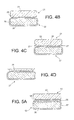
- FIGS. 3A to 3C show a first embodiment of the method of the invention
- FIGS. 4A to 4D show a second embodiment of the method of the invention
- FIGS. 5A to 5C show a third embodiment of the method of the invention
- FIG. 6 is a diagram showing the speed of etching of a chemical etching solution according to temperature
- FIGS. 7A to 7C show a fourth embodiment of the method of the invention.
- FIG. 8 shows a step of a fifth embodiment of the method of the invention.
- FIG. 9 shows a step of a variant of the fifth embodiment of the method of the invention.
- FIGS. 3A to 3C are cross sectional views showing a first embodiment of the method of the invention.
- FIG. 3A shows the assembly of a first wafer 11 and a second wafer 12 bonded to one another on the contact faces.
- Wafer 11 is a silicon wafer.
- Wafer 12 is a silicon wafer 13 covered with a layer of silicon oxide 14 .
- Bonding is achieved using a molecular adhesion technique well known to those skilled in the art. The adhesion is carried out for example at ambient temperature, and is then reinforced by heat treatment, for example between 900 and 1200° C. for 2 hours.
- the atmosphere of the heat treatment may be argon with approximately 2% oxygen (which is to say 98% argon and 2% oxygen in volume).
- Wafer 11 in silicon then undergoes de-oxidation to eliminate the native oxide, for example by HF diluted at 10%, and then chemical etching for example with the TMAH (tetramethylammonium hydroxide) or with KOH. It is also possible to carry out selective dry etching. All of the free surface of the wafer 11 undergoes this chemical etching and in particular the chamfered zone with the reference 15 in FIG. 3A .
- the chemical etching is carried out so as to obtain a pedestal 16 at the contact faces of the two wafers, wherein the pedestal rests entirely on the second wafer 12 (see FIG. 3B ). If the bond is strong enough, the width of the pedestal corresponds more or less to the bonding zone of the two wafers.
- the pedestal may be obtained by chemical etching of the wafer 11 on a thickness of around 80 ⁇ m.
- TMAH being used as the chemical etching product
- TMAH diluted to 25% may be used, at a temperature of 80° C. for 4 hours.
- This etching solution has the advantage of being highly selective (greater than 1000 between the silicon and the silicon oxide) and thus only etches very lightly the layer of oxide 14 of the wafer 12 .
- the silicon wafer 11 is made thinner on its free face, for example by mechanical action.
- a rapid grinding method may be used with a grinding wheel with a grain of around 50 ⁇ m (reference #325) for example.
- This grinding is completed by fine grinding which consists for example of grinding the thinned wafer with a grinding wheel with a grain of around 8 ⁇ m (reference #2000), or even finer.
- This step allows as much of the zone as possible that has been work hardened during the previous grinding operation to be removed.
- the etching step is carried out until the pedestal is reached.
- a final polishing step may be carried out to prepare a surface finish that is compatible for example with epitaxy.
- a surface finish is called “epi-ready” by those skilled in the art.
- the thickness that remains after the etching operations is determined according to the thickness required for the application in question.
- the thickness of the wafer 11 etched by the chemical etching solution is therefore also determined according to the desired thickness of the thin layer 17 (see FIG. 3C ).
- the pedestal will have, after the rapid grinding step, a thickness greater than the thickness of the thin layer 17 . It can then be seen that the edges of the SOI structure obtained are clean and well defined.
- the first wafer may be made of germanium and the second wafer made of silicon that may or may not be oxidised.
- Etching using H 2 O 2 heated to 70° C. permits the germanium to be etched to form the pedestal (for example 60 ⁇ m high). This etching has no effect on the second wafer that is made of silicon.
- the thinning may then permit a SGOI structure to be obtained, for example comprising a thin layer of germanium of between 10 and 40 ⁇ m thick.
- FIGS. 4A to 4D are cross sectional views illustrating a second embodiment of the method of the invention.
- FIG. 4A shows the assembly of a first wafer 21 and a second wafer 22 bonded to each other via the contact faces.
- the wafer 21 is a silicon wafer 23 covered with a silicon oxide layer 24 .
- the wafer 22 is also a silicon wafer 25 covered with a silicon oxide layer 26 .
- the silicon oxides 24 and 26 are either both heat treated oxides, or they are both deposited oxides but the thickness of the layer of oxide 24 is thinner than that of the layer of oxide 26 .
- the wafers 21 and have been bonded using a molecular adhesion technique at ambient temperature.
- the adhesion is strengthened by heat treatment, for example between 900 and 1200° C. for 2 hours.
- the atmosphere of the heat treatment may be argon with 2% oxygen (98% argon and 2% oxygen in volume).
- a first chemical etching operation is performed to deoxidise the free surface of the wafer 21 .
- HF diluted at 10% may be used.
- FIG. 4B shows that the free edges including the chamfered zones of the wafer 21 are deoxidised.
- a second chemical etching using TMAH diluted at 25% for example is then carried out, to reduce the thickness of silicon of the wafer 23 .
- All of the free surface of the silicon wafer 23 undergoes this chemical etching and in particular the lower chamfered zone 27 .
- the chemical etching is carried out so as to obtain part 28 of the pedestal at the contact faces des wafers 21 and 22 , wherein this part 28 rests entirely on the second wafer 22 by means of the remaining layer of oxide 24 (see FIG. 4C ).
- This may be obtained by chemical etching of the silicon 23 on a thickness for example of 80 ⁇ m.
- the etching solution may be at a temperature of 80° C. and the etching may last 4 hours.
- the following step consists of thinning the silicon wafer 23 that has already been partially thinned chemically.
- a fragile zone inside this wafer, for example by implanting gases (for example hydrogen) on the face to be assembled prior to bonding.
- This buried fragile zone is then fractured, for example by heat treatment and/or mechanically.
- FIG. 4D shows the structure obtained where the reference 29 designates the thin part of the first wafer.
- the thinning may also be obtained by various other techniques selected from chemical etching or dry etching (ionic, reactive ionic, etc.), or even “lift-off” techniques.
- FIGS. 5A to 5C are cross sectional views illustrating a third embodiment of the method of the invention.
- FIG. 5A shows the assembly of a first wafer 51 and a second wafer 52 bonded to one another via the contact faces.
- the wafer 51 comprises a support 53 , for example made of silicon, which successively supports a sacrificial layer 54 and a thin layer 55 . If the thin layer 55 is made of silicon, the sacrificial layer 54 may be made of porous silicon.
- the wafer 52 is a silicon wafer 56 covered by a protective layer made of silicon oxide 57 .
- the wafers 51 and 52 have been bonded to one another by a molecular adhesion technique at ambient temperature, wherein the thin layer 55 is brought into contact with the protective layer 57 .
- FIG. 5B shows the structure obtained after chemical etching designed to form the pedestal. All of the elements forming the wafer 51 have been etched. This figure shows that the pedestal of the first wafer 51 now rests entirely on the contact face of the second wafer 52 .
- the etching of the first wafer by a lift-off technique, by selectively etching the sacrificial layer 54 .
- the layer 54 is made of porous silicon and the thin layer 55 of silicon, the etching of the sacrificial layer 54 may be obtained by a mixture of water, HF and H 2 O 2 .
- the thin layer 55 can be made even thinner, for example mechanically.
- the temperature of the chemical etching solution (for example a TMAH solution at 25%) used to obtain the pedestal may be modified to modify the speed of the etching of the first wafer (for example made of silicon).
- FIG. 6 shows the rate of the etching speed graph V of the silicon by the TMAH according to the etching temperature T.
- the speed of etching of the solution may be modified if the composition of the etching solution changes.
- the various modes for using this etching solution allow the etching speed to be modified (for example recirculating to a greater or lesser extent the solution in an etching bath, the use of megasonics).
- the dimension of the silicon to be removed (80 ⁇ m in the previous examples) may vary from a few tens of micrometers to a few hundred micrometers.
- the minimum dimension to be achieved by this removal is advantageously around the dimension of the dimension to be achieved after the rapid etching of one of the wafers aimed at forming the thin part (or thin layer) of this wafer.
- the dimension to be removed may be 50 ⁇ m if the thin layer to be obtained is 20 ⁇ m.
- the fine thinning operation is carried out before reaching the pedestal.
- the temperature of the heat treatment used to strengthen the molecular adhesion may be situated in a very wide range, for example greater than 100° C.
- Various surface cleaning techniques may be used prior to the adhesion: chemical preparation of the surfaces, activation of the surfaces via plasma, UV, ozone, or possibly a combination.
- the adhesion may also be carried out in a partial vacuum.
- the lateral penetration of the etching solution at the bonding interface may be modified by modifying the adhesion energy of the two wafers.
- Lower energy leads to greater penetration of the etching solution at the bonding interface and thus requires more trimming by chemical etching.
- the thin layer obtained thus has a smaller diameter.
- the adhesion energy may thus be used as a means of controlling the width of the trimming.
- the nature of the protective layer may be modified and the etching solution may be adapted to carry out the lateral etching.
- etching methods may also be chosen to etch the protective layer and/or to create the pedestal to obtain a specific wafer edge required for the application in question (hollow or protruding).
- FIGS. 7A to 7C are cross sectional views illustrating a fourth embodiment of the method of the invention. These figures are to be compared with the FIGS. 4B to 4D .
- the lowering of the bonding energy between the first wafer 31 and the second wafer 32 allows lateral etching of the protective layer (in this example, of the oxide layer) by the first chemical etching that is more important than for the structure of FIG. 4B .
- the rest of the method is identical to the second embodiment.
- FIG. 7B the part 28 of the pedestal obtained after the second chemical etching.
- FIG. 7C the thinned part 39 of the first wafer.
- a fifth embodiment of the method of the invention consists of only removing the protective layer (the oxide layer) of the first wafer locally, for example next to the bonding interface.
- FIG. 8 This figure is a cross sectional view of an assembled structure comprising a first wafer 41 and a second wafer 42 bonded to one another on the contact faces.
- the wafer 41 is a silicon wafer 43 covered with a layer of oxide 44 .
- the wafer 42 is a silicon wafer 45 covered with a layer of oxide 46 .
- the layer of oxide 44 of the wafer 41 has only been eliminated next to the bonding interface, which has allowed a localised penetration zone to be created for the second chemical etching (chemical etching of the silicon 43 ). It is also possible to open locally the part of the layer 46 opposite the open zone of the layer 44 , which is to say on either side of the bonding interface. This is what is shown in FIG. 9 . Lateral soaking in a solution of HF at 10% for a calculated time permits the protective oxide to be removed. The structure obtained is then ready for the etching step that is for example mechanical.
- the method of the invention is suited to the creation of stacked structures of the silicon-on insulator type (SOI) with very thin surface film thicknesses (of around one to several micrometers) up to thicknesses of several tens of micrometers, or even several hundreds of micrometers.
- SOI silicon-on insulator type
- the method of the invention can be used for silicon wafers, as well as for other semiconductors (germanium, III-V semiconductors, etc.), for insulating materials (glass, quartz, ceramics, etc.), for piezoelectric materials (lithium niobate, lithium tantalate, etc.).
Landscapes
- Engineering & Computer Science (AREA)
- Microelectronics & Electronic Packaging (AREA)
- Condensed Matter Physics & Semiconductors (AREA)
- General Physics & Mathematics (AREA)
- Manufacturing & Machinery (AREA)
- Computer Hardware Design (AREA)
- Physics & Mathematics (AREA)
- Power Engineering (AREA)
- Weting (AREA)
- Micromachines (AREA)
- Bending Of Plates, Rods, And Pipes (AREA)
- Connection Of Plates (AREA)
- Surface Treatment Of Glass (AREA)
- Mechanical Treatment Of Semiconductor (AREA)
Abstract
Description
Claims (9)
Priority Applications (1)
| Application Number | Priority Date | Filing Date | Title |
|---|---|---|---|
| US13/682,009 US8628674B2 (en) | 2004-12-28 | 2012-11-20 | Method for trimming a structure obtained by the assembly of two plates |
Applications Claiming Priority (5)
| Application Number | Priority Date | Filing Date | Title |
|---|---|---|---|
| FR0413979 | 2004-12-28 | ||
| FR0413979A FR2880184B1 (en) | 2004-12-28 | 2004-12-28 | METHOD OF SORTING A STRUCTURE OBTAINED BY ASSEMBLING TWO PLATES |
| PCT/FR2005/051128 WO2006070160A1 (en) | 2004-12-28 | 2005-12-22 | Method for trimming a structure obtained by the assembly of two plates |
| US72211507A | 2007-06-19 | 2007-06-19 | |
| US13/682,009 US8628674B2 (en) | 2004-12-28 | 2012-11-20 | Method for trimming a structure obtained by the assembly of two plates |
Related Parent Applications (3)
| Application Number | Title | Priority Date | Filing Date |
|---|---|---|---|
| US11/722,115 Division US8329048B2 (en) | 2004-12-28 | 2005-12-22 | Method for trimming a structure obtained by the assembly of two plates |
| PCT/FR2005/051128 Division WO2006070160A1 (en) | 2004-12-28 | 2005-12-22 | Method for trimming a structure obtained by the assembly of two plates |
| US72211507A Division | 2004-12-28 | 2007-06-19 |
Publications (2)
| Publication Number | Publication Date |
|---|---|
| US20130078785A1 US20130078785A1 (en) | 2013-03-28 |
| US8628674B2 true US8628674B2 (en) | 2014-01-14 |
Family
ID=34953374
Family Applications (2)
| Application Number | Title | Priority Date | Filing Date |
|---|---|---|---|
| US11/722,115 Active 2028-07-14 US8329048B2 (en) | 2004-12-28 | 2005-12-22 | Method for trimming a structure obtained by the assembly of two plates |
| US13/682,009 Active US8628674B2 (en) | 2004-12-28 | 2012-11-20 | Method for trimming a structure obtained by the assembly of two plates |
Family Applications Before (1)
| Application Number | Title | Priority Date | Filing Date |
|---|---|---|---|
| US11/722,115 Active 2028-07-14 US8329048B2 (en) | 2004-12-28 | 2005-12-22 | Method for trimming a structure obtained by the assembly of two plates |
Country Status (8)
| Country | Link |
|---|---|
| US (2) | US8329048B2 (en) |
| EP (1) | EP1831923B1 (en) |
| JP (1) | JP5197017B2 (en) |
| KR (1) | KR101291086B1 (en) |
| CN (1) | CN101084577B (en) |
| FR (1) | FR2880184B1 (en) |
| SG (1) | SG159493A1 (en) |
| WO (1) | WO2006070160A1 (en) |
Cited By (4)
| Publication number | Priority date | Publication date | Assignee | Title |
|---|---|---|---|---|
| US20120161292A1 (en) * | 2010-12-20 | 2012-06-28 | Aomar Halimaoui | Process for assembling two wafers and corresponding device |
| US20150243551A1 (en) * | 2012-09-10 | 2015-08-27 | Soitec | Method of detaching a layer |
| US10679944B2 (en) * | 2018-09-21 | 2020-06-09 | United Microelectronics Corp. | Semiconductor structure with high resistivity wafer and fabricating method of bonding the same |
| DE102022000424A1 (en) | 2022-02-03 | 2023-08-03 | Azur Space Solar Power Gmbh | Manufacturing process for a semiconductor wafer with silicon and with a III-N layer |
Families Citing this family (43)
| Publication number | Priority date | Publication date | Assignee | Title |
|---|---|---|---|---|
| FR2880184B1 (en) | 2004-12-28 | 2007-03-30 | Commissariat Energie Atomique | METHOD OF SORTING A STRUCTURE OBTAINED BY ASSEMBLING TWO PLATES |
| US7981754B2 (en) * | 2006-09-07 | 2011-07-19 | Renesas Electronics Corporation | Manufacturing method of bonded SOI substrate and manufacturing method of semiconductor device |
| FR2935536B1 (en) * | 2008-09-02 | 2010-09-24 | Soitec Silicon On Insulator | PROGRESSIVE DETOURING METHOD |
| JP5244650B2 (en) * | 2009-02-26 | 2013-07-24 | 信越半導体株式会社 | Manufacturing method of SOI wafer |
| US8476165B2 (en) * | 2009-04-01 | 2013-07-02 | Tokyo Electron Limited | Method for thinning a bonding wafer |
| EP2461359B1 (en) | 2009-07-10 | 2017-02-08 | Shanghai Simgui Technology Co., Ltd | Method for forming substrate with insulating buried layer |
| FR2954585B1 (en) * | 2009-12-23 | 2012-03-02 | Soitec Silicon Insulator Technologies | METHOD FOR MAKING A HETEROSTRUCTURE WITH MINIMIZATION OF STRESS |
| FR2956822A1 (en) * | 2010-02-26 | 2011-09-02 | Soitec Silicon On Insulator Technologies | METHOD FOR REMOVING FRAGMENTS OF MATERIAL PRESENT ON THE SURFACE OF A MULTILAYER STRUCTURE |
| FR2957190B1 (en) | 2010-03-02 | 2012-04-27 | Soitec Silicon On Insulator | PROCESS FOR PRODUCING A MULTILAYER STRUCTURE WITH THERMOMECHANICAL EFFECT DETOURAGE |
| FR2967295B1 (en) * | 2010-11-05 | 2013-01-11 | Soitec Silicon On Insulator | PROCESS FOR PROCESSING A MULTILAYER STRUCTURE |
| US20120129318A1 (en) * | 2010-11-24 | 2012-05-24 | Semiconductor Energy Laboratory Co., Ltd. | Atmospheric pressure plasma etching apparatus and method for manufacturing soi substrate |
| JP2013008915A (en) * | 2011-06-27 | 2013-01-10 | Toshiba Corp | Substrate processing method and substrate processing apparatus |
| JP5946260B2 (en) * | 2011-11-08 | 2016-07-06 | 株式会社ディスコ | Wafer processing method |
| JP5978764B2 (en) | 2012-05-24 | 2016-08-24 | 信越半導体株式会社 | Manufacturing method of SOI wafer |
| US9343348B2 (en) * | 2012-06-12 | 2016-05-17 | Erich Thallner | Substrate-product substrate combination and device and method for producing a substrate-product substrate combination |
| US9064770B2 (en) * | 2012-07-17 | 2015-06-23 | Taiwan Semiconductor Manufacturing Company, Ltd. | Methods for minimizing edge peeling in the manufacturing of BSI chips |
| JP5862521B2 (en) | 2012-09-03 | 2016-02-16 | 信越半導体株式会社 | Manufacturing method of SOI wafer |
| CN104658927B (en) * | 2013-11-19 | 2018-03-30 | 中芯国际集成电路制造(上海)有限公司 | The bonding and wafer thinning optimization method of semiconductor wafer |
| CN104733300B (en) * | 2013-12-23 | 2018-09-25 | 中芯国际集成电路制造(上海)有限公司 | A kind of thining method of bonding wafer |
| FR3036223B1 (en) * | 2015-05-11 | 2018-05-25 | Commissariat A L'energie Atomique Et Aux Energies Alternatives | PROCESS FOR DIRECTLY BONDING SUBSTRATES WITH SHIFTING THE EDGES OF AT LEAST ONE OF THE TWO SUBSTRATES |
| US10134577B2 (en) * | 2015-05-21 | 2018-11-20 | Globalfoundries Inc. | Edge trim processes and resultant structures |
| JP6380245B2 (en) * | 2015-06-15 | 2018-08-29 | 信越半導体株式会社 | Manufacturing method of SOI wafer |
| CN105023839A (en) * | 2015-07-15 | 2015-11-04 | 中国电子科技集团公司第四十六研究所 | Method for manufacturing silicon chip of double-layer structure |
| US10867836B2 (en) * | 2016-05-02 | 2020-12-15 | Taiwan Semiconductor Manufacturing Co., Ltd. | Wafer stack and fabrication method thereof |
| US10204893B2 (en) | 2016-05-19 | 2019-02-12 | Invensas Bonding Technologies, Inc. | Stacked dies and methods for forming bonded structures |
| JP6202505B1 (en) * | 2016-06-17 | 2017-09-27 | 株式会社アイカムス・ラボ | Cell culture equipment |
| US20180019169A1 (en) * | 2016-07-12 | 2018-01-18 | QMAT, Inc. | Backing substrate stabilizing donor substrate for implant or reclamation |
| US20180182665A1 (en) | 2016-12-28 | 2018-06-28 | Invensas Bonding Technologies, Inc. | Processed Substrate |
| US10580823B2 (en) | 2017-05-03 | 2020-03-03 | United Microelectronics Corp. | Wafer level packaging method |
| US10879212B2 (en) * | 2017-05-11 | 2020-12-29 | Invensas Bonding Technologies, Inc. | Processed stacked dies |
| FR3076393A1 (en) * | 2017-12-28 | 2019-07-05 | Commissariat A L'energie Atomique Et Aux Energies Alternatives | METHOD OF TRANSFERRING A USEFUL LAYER |
| DE102018111200A1 (en) * | 2018-05-09 | 2019-11-14 | United Monolithic Semiconductors Gmbh | Method for producing an at least partially packaged semiconductor wafer |
| US11276676B2 (en) | 2018-05-15 | 2022-03-15 | Invensas Bonding Technologies, Inc. | Stacked devices and methods of fabrication |
| US11462419B2 (en) | 2018-07-06 | 2022-10-04 | Invensas Bonding Technologies, Inc. | Microelectronic assemblies |
| WO2020010136A1 (en) | 2018-07-06 | 2020-01-09 | Invensas Bonding Technologies, Inc. | Molded direct bonded and interconnected stack |
| US20200075533A1 (en) | 2018-08-29 | 2020-03-05 | Invensas Bonding Technologies, Inc. | Bond enhancement in microelectronics by trapping contaminants and arresting cracks during direct-bonding processes |
| FR3085957B1 (en) | 2018-09-14 | 2021-01-29 | Commissariat Energie Atomique | TEMPORARY BONDING PROCESS WITH THERMOPLASTIC ADHESIVE INCORPORATING A RIGID CROWN |
| WO2020150159A1 (en) | 2019-01-14 | 2020-07-23 | Invensas Bonding Technologies, Inc. | Bonded structures |
| US11296053B2 (en) | 2019-06-26 | 2022-04-05 | Invensas Bonding Technologies, Inc. | Direct bonded stack structures for increased reliability and improved yield in microelectronics |
| US12080672B2 (en) | 2019-09-26 | 2024-09-03 | Adeia Semiconductor Bonding Technologies Inc. | Direct gang bonding methods including directly bonding first element to second element to form bonded structure without adhesive |
| CN110739263A (en) * | 2019-10-28 | 2020-01-31 | 沈阳硅基科技有限公司 | Method for manufacturing SOI |
| US11631647B2 (en) | 2020-06-30 | 2023-04-18 | Adeia Semiconductor Bonding Technologies Inc. | Integrated device packages with integrated device die and dummy element |
| US11923205B2 (en) * | 2021-12-17 | 2024-03-05 | United Microelectronics Corporation | Method for manufacturing semiconductor device |
Citations (47)
| Publication number | Priority date | Publication date | Assignee | Title |
|---|---|---|---|---|
| US5032544A (en) | 1989-08-17 | 1991-07-16 | Shin-Etsu Handotai Co., Ltd. | Process for producing semiconductor device substrate using polishing guard |
| US5233218A (en) | 1990-09-20 | 1993-08-03 | Fujitsu Limited | Semiconductor wafer and process for producing same |
| US5258323A (en) | 1992-12-29 | 1993-11-02 | Honeywell Inc. | Single crystal silicon on quartz |
| US5340435A (en) | 1990-02-28 | 1994-08-23 | Yatsuo Ito | Bonded wafer and method of manufacturing it |
| US5395788A (en) | 1991-03-15 | 1995-03-07 | Shin Etsu Handotai Co., Ltd. | Method of producing semiconductor substrate |
| US5494849A (en) | 1995-03-23 | 1996-02-27 | Si Bond L.L.C. | Single-etch stop process for the manufacture of silicon-on-insulator substrates |
| US5665631A (en) | 1995-05-11 | 1997-09-09 | Samsung Electronics Co., Ltd. | SOI substrate manufacturing method |
| US5668045A (en) | 1994-11-30 | 1997-09-16 | Sibond, L.L.C. | Process for stripping outer edge of BESOI wafers |
| US5863829A (en) | 1995-08-24 | 1999-01-26 | Komatsu Electronic Metals Co., Ltd. | Process for fabricating SOI substrate |
| US5918139A (en) | 1997-01-31 | 1999-06-29 | Shin Etsu Handotai Co., Ltd. | Method of manufacturing a bonding substrate |
| US5937312A (en) | 1995-03-23 | 1999-08-10 | Sibond L.L.C. | Single-etch stop process for the manufacture of silicon-on-insulator wafers |
| EP0935280A1 (en) | 1998-02-04 | 1999-08-11 | Canon Kabushiki Kaisha | SOI substrate and method of manufacturing the same |
| US6004860A (en) | 1995-03-29 | 1999-12-21 | Komatsu Electronic Metals Co., Ltd. | SOI substrate and a method for fabricating the same |
| US6090688A (en) | 1996-11-15 | 2000-07-18 | Komatsu Electronic Metals Co., Ltd. | Method for fabricating an SOI substrate |
| EP1026728A2 (en) | 1999-02-02 | 2000-08-09 | Canon Kabushiki Kaisha | Substrate and method of manufacturing the same |
| US6110391A (en) | 1997-01-17 | 2000-08-29 | Shin-Etsu Handotai Co., Ltd. | Method of manufacturing a bonding substrate |
| US6214702B1 (en) | 1998-03-30 | 2001-04-10 | Samsung Electronics Co., Ltd. | Methods of forming semiconductor substrates using wafer bonding techniques and intermediate substrates formed thereby |
| US6291315B1 (en) | 1996-07-11 | 2001-09-18 | Denso Corporation | Method for etching trench in manufacturing semiconductor devices |
| US20010055854A1 (en) | 2000-03-31 | 2001-12-27 | Shoji Nishida | Process for producing semiconductor member, and process for producing solar cell |
| US20010055863A1 (en) | 1998-06-04 | 2001-12-27 | Masatake Nakano | Methods for manufacturing soi wafer and soi wafer |
| US20020023725A1 (en) | 1999-08-10 | 2002-02-28 | Michael Bryan | Nozzle for cleaving substrates |
| US6391743B1 (en) | 1998-09-22 | 2002-05-21 | Canon Kabushiki Kaisha | Method and apparatus for producing photoelectric conversion device |
| US20030008478A1 (en) * | 2000-03-29 | 2003-01-09 | Takao Abe | Production method for silicon wafer and soi wafer, and soi wafer |
| US20030087503A1 (en) * | 1994-03-10 | 2003-05-08 | Canon Kabushiki Kaisha | Process for production of semiconductor substrate |
| US6563172B2 (en) | 1998-01-13 | 2003-05-13 | Mitsubishi Denki Kabushiki Kaisha | Semiconductor substrate processing method |
| US20030102530A1 (en) | 1998-09-15 | 2003-06-05 | Kabushiki Kaisha Toshiba. | Semiconductor wafer, method of manufacturing the same and semiconductor device |
| US6830985B2 (en) | 2000-04-28 | 2004-12-14 | Sumitomo Mitsubishi Silicon Corporation | Method and apparatus for producing bonded dielectric separation wafer |
| US6841848B2 (en) | 2003-06-06 | 2005-01-11 | Analog Devices, Inc. | Composite semiconductor wafer and a method for forming the composite semiconductor wafer |
| US6844242B2 (en) | 2001-07-13 | 2005-01-18 | Renesas Technology Corp. | Method of manufacturing SOI wafer |
| US20050112847A1 (en) | 2003-09-30 | 2005-05-26 | Commissariat A L'energie Atomique | Method for separating wafers bonded together to form a stacked structure |
| US6900114B2 (en) * | 1999-02-02 | 2005-05-31 | Canon Kabushiki Kaisha | Separating apparatus, separating method, and method of manufacturing semiconductor substrate |
| US6953948B2 (en) | 2000-01-07 | 2005-10-11 | Canon Kabushiki Kaisha | Semiconductor substrate and process for its production |
| US20060055003A1 (en) | 2004-05-19 | 2006-03-16 | Sumco Corporation | Bonded SOI substrate, and method for manufacturing the same |
| US20060128078A1 (en) * | 2004-12-15 | 2006-06-15 | Ryuji Moriwaki | SOI substrate manufacturing method |
| US7195988B2 (en) | 2003-07-01 | 2007-03-27 | Renesas Technology Corp. | Semiconductor wafer and method of manufacturing a semiconductor device using a separation portion on a peripheral area of the semiconductor wafer |
| US20070072393A1 (en) | 2003-10-14 | 2007-03-29 | Tracit Technologies | Method for preparing and assembling substrates |
| US20070148914A1 (en) * | 2005-12-22 | 2007-06-28 | Etsurou Morita | Process for Regeneration of a Layer Transferred Wafer and Regenerated Layer Transferred Wafer |
| US7285825B2 (en) * | 2003-01-21 | 2007-10-23 | Kabushiki Kaisha Toshiba | Element formation substrate for forming semiconductor device |
| US20080036041A1 (en) * | 2003-11-28 | 2008-02-14 | Roy Knechtel | Production Of Semiconductor Substrates With Buried Layers By Joining (Bonding) Semiconductor Wafers |
| US7399693B2 (en) * | 2004-06-23 | 2008-07-15 | Canon Kabushiki Kaisha | Semiconductor film manufacturing method and substrate manufacturing method |
| US7452584B2 (en) * | 2002-07-17 | 2008-11-18 | S.O.I. Tec Silicon On Insulator Technologies | Method of increasing the area of a useful layer of material transferred onto a support |
| US20090095399A1 (en) | 2004-12-28 | 2009-04-16 | Commissariat A L'energie Atomique | Method for trimming a structure obtained by the assembly of two plates |
| US7572714B2 (en) * | 2005-07-08 | 2009-08-11 | S.O.I.Tec Silicon On Insulator Technologies | Film taking-off method |
| US7727860B2 (en) | 2005-05-31 | 2010-06-01 | Shin-Etsu Handotai Co., Ltd. | Method for manufacturing bonded wafer and outer-peripheral grinding machine of bonded wafer |
| US7749861B2 (en) | 2005-12-19 | 2010-07-06 | Shin-Etsu Handotai Co., Ltd. | Method for manufacturing SOI substrate and SOI substrate |
| US7851330B2 (en) * | 2004-11-09 | 2010-12-14 | S.O.I.Tec Silicon On Insulator Technologies | Methods for fabricating compound material wafers |
| US7855129B2 (en) * | 2005-12-22 | 2010-12-21 | Sumco Corporation | Method for manufacturing direct bonded SOI wafer and direct bonded SOI wafer manufactured by the method |
Family Cites Families (1)
| Publication number | Priority date | Publication date | Assignee | Title |
|---|---|---|---|---|
| JP3496925B2 (en) * | 1998-02-04 | 2004-02-16 | キヤノン株式会社 | Semiconductor substrate and manufacturing method thereof |
-
2004
- 2004-12-28 FR FR0413979A patent/FR2880184B1/en not_active Expired - Fee Related
-
2005
- 2005-12-22 KR KR1020077014025A patent/KR101291086B1/en active IP Right Grant
- 2005-12-22 SG SG201000395-2A patent/SG159493A1/en unknown
- 2005-12-22 WO PCT/FR2005/051128 patent/WO2006070160A1/en active Application Filing
- 2005-12-22 US US11/722,115 patent/US8329048B2/en active Active
- 2005-12-22 CN CN200580044108XA patent/CN101084577B/en active Active
- 2005-12-22 EP EP05825588.6A patent/EP1831923B1/en active Active
- 2005-12-22 JP JP2007548879A patent/JP5197017B2/en active Active
-
2012
- 2012-11-20 US US13/682,009 patent/US8628674B2/en active Active
Patent Citations (56)
| Publication number | Priority date | Publication date | Assignee | Title |
|---|---|---|---|---|
| US5032544A (en) | 1989-08-17 | 1991-07-16 | Shin-Etsu Handotai Co., Ltd. | Process for producing semiconductor device substrate using polishing guard |
| US5340435A (en) | 1990-02-28 | 1994-08-23 | Yatsuo Ito | Bonded wafer and method of manufacturing it |
| US5233218A (en) | 1990-09-20 | 1993-08-03 | Fujitsu Limited | Semiconductor wafer and process for producing same |
| US5395788A (en) | 1991-03-15 | 1995-03-07 | Shin Etsu Handotai Co., Ltd. | Method of producing semiconductor substrate |
| US5258323A (en) | 1992-12-29 | 1993-11-02 | Honeywell Inc. | Single crystal silicon on quartz |
| US20030087503A1 (en) * | 1994-03-10 | 2003-05-08 | Canon Kabushiki Kaisha | Process for production of semiconductor substrate |
| US5668045A (en) | 1994-11-30 | 1997-09-16 | Sibond, L.L.C. | Process for stripping outer edge of BESOI wafers |
| US5834812A (en) | 1994-11-30 | 1998-11-10 | Sibond, L.L.C. | Edge stripped BESOI wafer |
| US5937312A (en) | 1995-03-23 | 1999-08-10 | Sibond L.L.C. | Single-etch stop process for the manufacture of silicon-on-insulator wafers |
| US5494849A (en) | 1995-03-23 | 1996-02-27 | Si Bond L.L.C. | Single-etch stop process for the manufacture of silicon-on-insulator substrates |
| US6004860A (en) | 1995-03-29 | 1999-12-21 | Komatsu Electronic Metals Co., Ltd. | SOI substrate and a method for fabricating the same |
| US5665631A (en) | 1995-05-11 | 1997-09-09 | Samsung Electronics Co., Ltd. | SOI substrate manufacturing method |
| US5863829A (en) | 1995-08-24 | 1999-01-26 | Komatsu Electronic Metals Co., Ltd. | Process for fabricating SOI substrate |
| US6291315B1 (en) | 1996-07-11 | 2001-09-18 | Denso Corporation | Method for etching trench in manufacturing semiconductor devices |
| US6090688A (en) | 1996-11-15 | 2000-07-18 | Komatsu Electronic Metals Co., Ltd. | Method for fabricating an SOI substrate |
| US6110391A (en) | 1997-01-17 | 2000-08-29 | Shin-Etsu Handotai Co., Ltd. | Method of manufacturing a bonding substrate |
| US5918139A (en) | 1997-01-31 | 1999-06-29 | Shin Etsu Handotai Co., Ltd. | Method of manufacturing a bonding substrate |
| US6872979B2 (en) | 1998-01-13 | 2005-03-29 | Renesas Technology Corp. | Semiconductor substrate with stacked oxide and SOI layers with a molten or epitaxial layer formed on an edge of the stacked layers |
| US6563172B2 (en) | 1998-01-13 | 2003-05-13 | Mitsubishi Denki Kabushiki Kaisha | Semiconductor substrate processing method |
| EP0935280A1 (en) | 1998-02-04 | 1999-08-11 | Canon Kabushiki Kaisha | SOI substrate and method of manufacturing the same |
| US6214702B1 (en) | 1998-03-30 | 2001-04-10 | Samsung Electronics Co., Ltd. | Methods of forming semiconductor substrates using wafer bonding techniques and intermediate substrates formed thereby |
| US20010055863A1 (en) | 1998-06-04 | 2001-12-27 | Masatake Nakano | Methods for manufacturing soi wafer and soi wafer |
| US6534384B2 (en) | 1998-06-04 | 2003-03-18 | Shin-Etsu Handotai Co., Ltd. | Method for manufacturing SOI wafer including heat treatment in an oxidizing atmosphere |
| US20030102530A1 (en) | 1998-09-15 | 2003-06-05 | Kabushiki Kaisha Toshiba. | Semiconductor wafer, method of manufacturing the same and semiconductor device |
| US6391743B1 (en) | 1998-09-22 | 2002-05-21 | Canon Kabushiki Kaisha | Method and apparatus for producing photoelectric conversion device |
| US6624047B1 (en) | 1999-02-02 | 2003-09-23 | Canon Kabushiki Kaisha | Substrate and method of manufacturing the same |
| EP1026728A2 (en) | 1999-02-02 | 2000-08-09 | Canon Kabushiki Kaisha | Substrate and method of manufacturing the same |
| US6900114B2 (en) * | 1999-02-02 | 2005-05-31 | Canon Kabushiki Kaisha | Separating apparatus, separating method, and method of manufacturing semiconductor substrate |
| US20020023725A1 (en) | 1999-08-10 | 2002-02-28 | Michael Bryan | Nozzle for cleaving substrates |
| US6953948B2 (en) | 2000-01-07 | 2005-10-11 | Canon Kabushiki Kaisha | Semiconductor substrate and process for its production |
| US20030008478A1 (en) * | 2000-03-29 | 2003-01-09 | Takao Abe | Production method for silicon wafer and soi wafer, and soi wafer |
| US20010055854A1 (en) | 2000-03-31 | 2001-12-27 | Shoji Nishida | Process for producing semiconductor member, and process for producing solar cell |
| US6830985B2 (en) | 2000-04-28 | 2004-12-14 | Sumitomo Mitsubishi Silicon Corporation | Method and apparatus for producing bonded dielectric separation wafer |
| US6844242B2 (en) | 2001-07-13 | 2005-01-18 | Renesas Technology Corp. | Method of manufacturing SOI wafer |
| US7452584B2 (en) * | 2002-07-17 | 2008-11-18 | S.O.I. Tec Silicon On Insulator Technologies | Method of increasing the area of a useful layer of material transferred onto a support |
| US7285825B2 (en) * | 2003-01-21 | 2007-10-23 | Kabushiki Kaisha Toshiba | Element formation substrate for forming semiconductor device |
| US7510945B2 (en) * | 2003-01-21 | 2009-03-31 | Kabushiki Kaisha Toshiba | Element formation substrate, method of manufacturing the same, and semiconductor device |
| US6841848B2 (en) | 2003-06-06 | 2005-01-11 | Analog Devices, Inc. | Composite semiconductor wafer and a method for forming the composite semiconductor wafer |
| US7195988B2 (en) | 2003-07-01 | 2007-03-27 | Renesas Technology Corp. | Semiconductor wafer and method of manufacturing a semiconductor device using a separation portion on a peripheral area of the semiconductor wafer |
| US20050112847A1 (en) | 2003-09-30 | 2005-05-26 | Commissariat A L'energie Atomique | Method for separating wafers bonded together to form a stacked structure |
| US7264996B2 (en) | 2003-09-30 | 2007-09-04 | Commissariat A L'energie Atomique | Method for separating wafers bonded together to form a stacked structure |
| US20070072393A1 (en) | 2003-10-14 | 2007-03-29 | Tracit Technologies | Method for preparing and assembling substrates |
| US20080036041A1 (en) * | 2003-11-28 | 2008-02-14 | Roy Knechtel | Production Of Semiconductor Substrates With Buried Layers By Joining (Bonding) Semiconductor Wafers |
| US20060055003A1 (en) | 2004-05-19 | 2006-03-16 | Sumco Corporation | Bonded SOI substrate, and method for manufacturing the same |
| US7442992B2 (en) | 2004-05-19 | 2008-10-28 | Sumco Corporation | Bonded SOI substrate, and method for manufacturing the same |
| US20090093106A1 (en) | 2004-05-19 | 2009-04-09 | Sumco Corporation | Bonded soi substrate, and method for manufacturing the same |
| US7399693B2 (en) * | 2004-06-23 | 2008-07-15 | Canon Kabushiki Kaisha | Semiconductor film manufacturing method and substrate manufacturing method |
| US7851330B2 (en) * | 2004-11-09 | 2010-12-14 | S.O.I.Tec Silicon On Insulator Technologies | Methods for fabricating compound material wafers |
| US7368332B2 (en) | 2004-12-15 | 2008-05-06 | Canon Kabushiki Kaisha | SOI substrate manufacturing method |
| US20060128078A1 (en) * | 2004-12-15 | 2006-06-15 | Ryuji Moriwaki | SOI substrate manufacturing method |
| US20090095399A1 (en) | 2004-12-28 | 2009-04-16 | Commissariat A L'energie Atomique | Method for trimming a structure obtained by the assembly of two plates |
| US7727860B2 (en) | 2005-05-31 | 2010-06-01 | Shin-Etsu Handotai Co., Ltd. | Method for manufacturing bonded wafer and outer-peripheral grinding machine of bonded wafer |
| US7572714B2 (en) * | 2005-07-08 | 2009-08-11 | S.O.I.Tec Silicon On Insulator Technologies | Film taking-off method |
| US7749861B2 (en) | 2005-12-19 | 2010-07-06 | Shin-Etsu Handotai Co., Ltd. | Method for manufacturing SOI substrate and SOI substrate |
| US20070148914A1 (en) * | 2005-12-22 | 2007-06-28 | Etsurou Morita | Process for Regeneration of a Layer Transferred Wafer and Regenerated Layer Transferred Wafer |
| US7855129B2 (en) * | 2005-12-22 | 2010-12-21 | Sumco Corporation | Method for manufacturing direct bonded SOI wafer and direct bonded SOI wafer manufactured by the method |
Non-Patent Citations (1)
| Title |
|---|
| U.S. Appl. No. 13/699,154, filed Nov. 20, 2012, Fournel, et al. |
Cited By (6)
| Publication number | Priority date | Publication date | Assignee | Title |
|---|---|---|---|---|
| US20120161292A1 (en) * | 2010-12-20 | 2012-06-28 | Aomar Halimaoui | Process for assembling two wafers and corresponding device |
| US9330957B2 (en) * | 2010-12-20 | 2016-05-03 | Stmicroelectronics (Crolles 2) Sas | Process for assembling two wafers and corresponding device |
| US20150243551A1 (en) * | 2012-09-10 | 2015-08-27 | Soitec | Method of detaching a layer |
| US9275893B2 (en) * | 2012-09-10 | 2016-03-01 | Soitec | Method of detaching a layer |
| US10679944B2 (en) * | 2018-09-21 | 2020-06-09 | United Microelectronics Corp. | Semiconductor structure with high resistivity wafer and fabricating method of bonding the same |
| DE102022000424A1 (en) | 2022-02-03 | 2023-08-03 | Azur Space Solar Power Gmbh | Manufacturing process for a semiconductor wafer with silicon and with a III-N layer |
Also Published As
| Publication number | Publication date |
|---|---|
| EP1831923A1 (en) | 2007-09-12 |
| FR2880184A1 (en) | 2006-06-30 |
| CN101084577B (en) | 2010-06-16 |
| US8329048B2 (en) | 2012-12-11 |
| US20090095399A1 (en) | 2009-04-16 |
| WO2006070160A1 (en) | 2006-07-06 |
| FR2880184B1 (en) | 2007-03-30 |
| JP5197017B2 (en) | 2013-05-15 |
| KR101291086B1 (en) | 2013-08-01 |
| KR20070110261A (en) | 2007-11-16 |
| EP1831923B1 (en) | 2019-05-22 |
| US20130078785A1 (en) | 2013-03-28 |
| JP2008526038A (en) | 2008-07-17 |
| SG159493A1 (en) | 2010-03-30 |
| CN101084577A (en) | 2007-12-05 |
Similar Documents
| Publication | Publication Date | Title |
|---|---|---|
| US8628674B2 (en) | Method for trimming a structure obtained by the assembly of two plates | |
| EP1929511B1 (en) | Semiconductor on glass insulator with deposited barrier layer | |
| KR101151458B1 (en) | Method for manufacturing bonded wafer and bonded wafer | |
| US6204079B1 (en) | Selective transfer of elements from one support to another support | |
| KR101185426B1 (en) | A mixed trimming method | |
| US8202785B2 (en) | Surface treatment for molecular bonding | |
| KR102658526B1 (en) | Method for manufacturing composite wafer with oxide single crystal thin film | |
| US20070072393A1 (en) | Method for preparing and assembling substrates | |
| EP1798765A2 (en) | Semiconductor on glass insulator made using improved ion implantation process | |
| KR102552244B1 (en) | Process for transferring thin layers to supporting substrates with different coefficients of thermal expansion | |
| KR101487371B1 (en) | Method for Recycling a Substrate, Laminated Wafer Fabricating Method and Suitable Recycled Donor Substrate | |
| KR101541940B1 (en) | Method for producing soi substrate | |
| KR101526245B1 (en) | Process for fabricating a semiconductor structure employing a temporary bond | |
| JP2005505935A (en) | Method for manufacturing a thin film layer containing microcomponents | |
| WO2010057941A1 (en) | A method of producing a silicon-on-sapphire type heterostructure. | |
| JP2010538459A (en) | Reuse of semiconductor wafers in delamination processes using heat treatment | |
| JP4987470B2 (en) | Method for producing ultrathin layer thinned by inducing self-supporting | |
| JP7206465B2 (en) | Masking of zones at the edges of the donor substrate during the ion implantation step | |
| US7816233B2 (en) | Method of manufacturing composite wafer structure | |
| US11610808B2 (en) | Semiconductor wafer with low defect count and method for manufacturing thereof | |
| JP4531694B2 (en) | Method for expanding the area of a useful layer of material that is transferred to a support | |
| US7811901B1 (en) | Method and edge region structure using co-implanted particles for layer transfer processes | |
| KR102568640B1 (en) | Method for producing the remainder of the donor substrate, substrate produced by the method and use of the substrate | |
| CN111630653B (en) | Separable structure and separation method using the same | |
| WO2012059350A2 (en) | A method of treating a multilayer structure |
Legal Events
| Date | Code | Title | Description |
|---|---|---|---|
| AS | Assignment |
Owner name: SOITEC, FRANCE Free format text: CHANGE OF NAME;ASSIGNOR:S.O.I. TEC SILICON ON INSULATOR TECHNOLOGIES;REEL/FRAME:029779/0440 Effective date: 20110624 |
|
| AS | Assignment |
Owner name: COMMISSARIAT A L'ENERGIE ATOMIQUE ET AUX ENERGIES Free format text: CHANGE OF NAME;ASSIGNOR:COMMISSARIAT A L'ENERGIE ATOMIQUE;REEL/FRAME:030352/0055 Effective date: 20100309 |
|
| STCF | Information on status: patent grant |
Free format text: PATENTED CASE |
|
| FPAY | Fee payment |
Year of fee payment: 4 |
|
| MAFP | Maintenance fee payment |
Free format text: PAYMENT OF MAINTENANCE FEE, 8TH YEAR, LARGE ENTITY (ORIGINAL EVENT CODE: M1552); ENTITY STATUS OF PATENT OWNER: LARGE ENTITY Year of fee payment: 8 |