RELATED APPLICATIONS
This application is a Divisional patent application of application Ser. No. 12/457,222, filed on 4 Jun. 2009, now pending. The entire disclosure of the prior application, Ser. No. 12/457,222, from which an oath or declaration is supplied, is considered a part of the disclosure of the accompanying Divisional application and is hereby incorporated by reference.
BACKGROUND OF THE INVENTION
1. Field of the Invention
The present invention relates to an LED chip package structure and a method for making the same, and particularly relates to an LED chip package structure using sedimentation and a method for making the same.
2. Description of Related Art
Referring to FIG. 1, a known LED package structure includes a substrate 1, an LED 2 disposed on the substrate 1, two wires 3, and a colloid layer 4 with phosphor powder 40.
The LED 2 has a light-emitting surface 20 opposite to the substrate 1. The LED 2 has a positive electrode area 21 and a negative electrode area 22 electrically connected to two corresponding positive and negative electrode areas 11, 12 of the substrate 1 via the two 3 respectively. Moreover, the colloid layer 4 with the phosphor powder 40 covers the LED 2 and the two wires 3 for protecting the LED 2. Therefore, when the LED 2 is a blue LED, the blue light generated by the blue LED can pass through the colloid layer 4 with the phosphor powder 40 to generate white light.
However, the phosphor powder 40 does not be uniformly mixed into the colloid layer 4. Hence, when the blue light generated by the blue LED can pass through the colloid layer 4 with the phosphor powder 40 to generate white light, “the condensing capability” and “the color and luster” of the white light are bad and non-uniform.
SUMMARY OF THE INVENTION
One particular aspect of the present invention is to provide an LED chip package structure using sedimentation and a method for making the same. Because the powder of the present invention can be fully deposited on the inner surface of the package body, “the condensing capability” and “the color and luster” of the present invention are good and uniform. In other words, the powder of the present invention can be fully deposited on the inner surface of the package body, so that light generated by the light-emitting elements can pass through the uniform package colloid layer to project uniform light beams out. Hence, the present invention can generate a best light-projecting quality.
In order to achieve the above-mentioned aspects, the present invention provides an LED chip package structure using sedimentation, including: a package body, at least two conductive substrates, at least one light-emitting element, and a package unit. The package body has a receiving space. The two conductive substrates are received in the receiving space. The light-emitting element is received in the receiving space and electrically connected to the two conductive substrates. The powder is uniformly deposited in the receiving space by maintaining the package unit at room temperature firstly and the powder is solidified in the receiving space by heating to a predetermined temperature.
Moreover, the package unit has the following three aspects:
1. First aspect: The package unit has a package colloid layer and a powder mixed into the package colloid layer, and the package unit is filled into the receiving space.
2. Second aspect: The package unit has a package colloid layer with powder and a transparent colloid layer received in the receiving space. The light-emitting element is covered by the package colloid layer with the powder, and the transparent colloid layer is disposed on the package colloid layer in order to protect the package colloid layer.
3. Third aspect: The package unit has a package colloid layer with powder and a transparent colloid layer received in the receiving space. The light-emitting element is covered by the transparent colloid layer, and the package colloid layer is disposed on the transparent colloid layer in order to prevent the quality of the package colloid layer from being affected by heat generated by the light-emitting element.
In order to achieve the above-mentioned aspects, the present invention provides a method for making an LED chip package structure using sedimentation, including: receiving at least one light-emitting element in a receiving space of a package body; electrically connecting the light-emitting element with two conductive substrates that are received in the receiving space; filling a package colloid layer with powder into the receiving space; and maintaining the package colloid layer with the powder at room temperature in order to uniformly depositing the powder in the receiving space.
Moreover, after the step of maintaining the package colloid layer, the method further includes heating the package colloid layer with the powder in order to solidify the package colloid layer with the powder in the receiving space. In addition, the step of heating the package colloid layer is a one-step heating process that includes a heating temperature of 80˜150° C. and a heating time of 1˜6 hours; Alternatively, the step of heating the package colloid layer is a two-step heating process that includes a first-step heating process and a second-step heating process, the first-step heating process has a heating temperature of 30˜100° C. and a heating time of 10˜120 minutes, and the second-step heating process has a heating temperature of 80˜150° C. and a heating time of 1˜6 hours.
Furthermore, after the step of heating the package colloid layer, the method further includes: filling a transparent colloid layer in the receiving space of the package body in order to form the transparent colloid layer on the package colloid layer with the powder; and heating the transparent colloid layer to 80-150° C. during 1-6 hours in order to solidify the transparent colloid layer.
In addition, in another embodiment, before the step of filling the package colloid layer with the powder into the receiving space, the method further includes: filling a transparent colloid layer in the receiving space of the package body in order to cover the light-emitting element; and heating the transparent colloid layer to 80-150° C. during 1-6 hours in order to solidify the transparent colloid layer, wherein the package colloid layer is disposed on the transparent colloid layer.
Therefore, the package colloid layer with the powder is fully deposited firstly, and then the package colloid layer with the powder is heated, in order to make the powder be fully deposited in the receiving space of the package body. Hence, the present invention can prevent non-deposited powder from be solidified in the receiving space of the package body. In addition, the curing time can be decreased, so that the usage life of the package colloid layer with the powder is increased.
Furthermore, the present invention has the following three deposition types according to different light-projecting properties and package structures
1. First type is a single deposition as the first embodiment. The advantage is: the manufacture process is simple.
2. Second type is a dual-layer structure with an inner deposition as the second embodiment. The advantage is: the dual-layer structure has two colloid layers that have the same or different physical property and chemical property such as adhesiveness, hardness or refractive index etc. In addition, the optical quality and the package structure of the second type are good.
3. Third type is a dual-layer structure with an outer deposition as the third embodiment. The advantage is: the package colloid layer is disposed on the transparent colloid layer in order to prevent the quality and the usage life of the package colloid layer from being affected (decreased) by heat generated by the light-emitting element.
It is to be understood that both the foregoing general description and the following detailed description are exemplary, and are intended to provide further explanation of the invention as claimed. Other advantages and features of the invention will be apparent from the following description, drawings and claims.
BRIEF DESCRIPTION OF THE DRAWINGS
The various objects and advantages of the present invention will be more readily understood from the following detailed description when read in conjunction with the appended drawings, in which:
FIG. 1 is a lateral, schematic view of an LED package structure by wire-bounding according to the prior art;
FIG. 2 is a flowchart of a method for making an LED chip package structure using sedimentation according to the first embodiment of the present invention;
FIGS. 2A to 2C are cross-sectional views of an LED chip package structure using sedimentation according to the first embodiment of the present invention, at different stages of the packaging processes, respectively;
FIG. 3 is a flowchart of a method for making an LED chip package structure using sedimentation according to the second embodiment of the present invention;
FIGS. 3A to 3C are cross-sectional views of an LED chip package structure using sedimentation according to the second embodiment of the present invention, at different stages of the packaging processes, respectively;
FIG. 4 is a flowchart of a method for making an LED chip package structure using sedimentation according to the third embodiment of the present invention;
FIGS. 4A to 4C are cross-sectional views of an LED chip package structure using sedimentation according to the third embodiment of the present invention, at different stages of the packaging processes, respectively;
FIGS. 5A and 5B are schematic views of a first method for depositing the powder according to the present invention, respectively;
FIGS. 6A and 6B are schematic views of a second method for depositing the powder according to the present invention, respectively; and
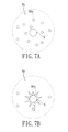
FIGS. 7A and 7B are schematic views of a third method for depositing the powder according to the present invention, respectively.
DETAILED DESCRIPTION OF THE PREFERRED EMBODIMENTS
Referring to FIGS. 2 and 2A to 2C, the first embodiment of the present invention provides a method for making an LED chip package structure using sedimentation, including the following steps:
Step S100 is: referring to FIGS. 2 and 2A, receiving at least one light-emitting element 1 a in a receiving space 20 a of a package body 2 a. In the first embodiment, the light-emitting element 1 a can be a blue LED, and the package body 2 a has a bowl shape. In addition, the light-emitting element 1 a is firmly fixed on the inner surface of the bowl-shaped package body 2 a via a chip-positioning layer 3 a formed between the light-emitting element 1 a and the package body 2 a. Moreover, the chip-positioning layer 3 a is solidified by curing to 155° C. during 3 hours in order to firmly fix the light-emitting element 1 a on the inner surface of the bowl-shaped package body 2 a.
Step S102 is: referring to FIGS. 2 and 2A, electrically connecting the light-emitting element 1 a with two conductive substrates (40 a, 41 a) that are received in the receiving space 20 a. In the first embodiment, at least two lead wires 5 a are electrically connected between the light-emitting element 1 a and one conductive substrate (positive electrode) 40 a and between the light-emitting element 1 a and one conductive substrate (negative electrode) 41 a. Hence, the positive electrode (not shown) and the negative electrode (not shown) of the light-emitting element 1 a are respectively electrically connected with the two conductive substrates (40 a, 41 a) by wire-bonding.
Step S104 is: referring to FIGS. 2 and 2B, filling a package colloid layer 6 a with powder 60 a (the package unit) into the receiving space 20 a. In the first embodiment, the powder 60 a can be phosphor powder, and the package colloid layer 6 a can be silicone or epoxy. In addition, the package colloid layer 6 a with the powder 60 a can be filled into the receiving space 20 a by dropping, press molding or spraying according to different requirements.
Step S106 is: referring to FIGS. 2 and 2C, maintaining the package colloid layer 6 a with the powder 60 a at room temperature in order to uniformly depositing the powder 60 a′ in the receiving space 20 a. In other words, the powder 60 a′ can be deposited on the light-emitting element 1 a, the two conductive substrates (40 a, 41 a) and an inner surface of the package body 2 a. In addition, the room temperature is defined as 13-25° C., and the package colloid layer 6 a is maintained at 1-168 hours according the properties of the package colloid layer 6 a.
Step S108 is: heating the package colloid layer 6 a′ with the powder 60 a′ in order to solidify the package colloid layer 6 a′ with the powder 60 a′ in the receiving space 20 a. The heating step includes the following two methods according to different manufacturing requirements:
1. The step of heating the package colloid layer 6 a′ is a one-step heating process that includes a heating temperature of 80˜150° C. and a heating time of 1˜6 hours.
2. The step of heating the package colloid layer 6 a′ is a two-step heating process that includes a first-step heating process and a second-step heating process, the first-step heating process has a heating temperature of 30˜100° C. and a heating time of 10˜120 minutes, and the second-step heating process has a heating temperature of 80˜150° C. and a heating time of 1˜6 hours.
In other words, the package colloid layer 6 a with the powder 60 a is fully deposited firstly as shown in FIG. 2B, and then the package colloid layer 6 a′ with the powder 60 a′ is heated as shown in FIG. 2C, in order to make the powder 60 a be fully deposited as the powder 60 a′ on the inner surface of the package body 2 a. Hence, the present invention can prevent non-deposited powder from be solidified in the inner surface of the package body 2 a.
Referring to FIG. 2C, the first embodiment of the present invention provides an LED chip package structure using sedimentation, including: at least one light-emitting element 1 a, a package body 2 a, at least two conductive substrates (40 a, 41 a), and a package unit. The package body 2 a has a receiving space 20 a. The two conductive substrates (40 a, 41 a) are received in the receiving space 20 a. The light-emitting element 1 a is received in the receiving space 20 a and electrically connected to the two conductive substrates (40 a, 41 a). The package unit has a package colloid layer 6 a′ and a powder 60 a′ mixed into the package colloid layer 6 a′. The package unit is filled into the receiving space 20 a, and the powder 60 a′ are uniformly deposited in the receiving space 20 a by maintaining the package unit at room temperature firstly and the powder 60 a′ are solidified in the receiving space 20 a by heating to a predetermined temperature.
Referring to FIGS. 3 and 3A to 3C, the steps of S200 to S202 in the second embodiment are the same as the steps of S100 to S102 in the first embodiment.
Moreover, after the step of S202, the second embodiment of the present invention further includes the following steps:
Step S204 is: referring to FIGS. 3 and 3A, filling a package colloid layer 6 b with powder 60 b into one part of a receiving space 20 b of a package body 2 b.
Step S206 is: referring to FIGS. 3 and 3B, maintaining the package colloid layer 6 b with the powder 60 b at room temperature in order to uniformly depositing the powder 60 b′ in one part of the receiving space 20 b. In other words, the powder 60 b′ can be deposited on a light-emitting element 1 b, two conductive substrates (40 b, 41 b) and an inner surface of the package body 2 b. In addition, the room temperature is defined as 13-25° C., and the package colloid layer 6 b is maintained at 1-168 hours according the properties of the package colloid layer 6 b.
Step S208 is: heating the package colloid layer 6 b′ with the powder 60 b′ in order to solidify the package colloid layer 6 b′ with the powder 60 b′. In other words, the package colloid layer 6 b with the powder 60 b is fully deposited firstly as shown in FIG. 3A, and then the package colloid layer 6 b′ with the powder 60 b′ is heated as shown in FIG. 3B, in order to make the powder 60 b be fully deposited as the powder 60 b′ on one part of the inner surface of the package body 2 b. Hence, the present invention can prevent non-deposited powder from be solidified in the inner surface of the package body 2 b.
Step S210 is: referring to FIGS. 3 and 3C, filling a transparent colloid layer 7 b in the other part of the receiving space 20 b of the package body 2 b in order to form the transparent colloid layer 7 b on the package colloid layer 6 b′ with the powder 60 b′.
Step S212 is: heating the transparent colloid layer 7 b to 80-150° C. during 1-6 hours in order to solidify the transparent colloid layer 7 b.
Referring to FIG. 3C, the second embodiment of the present invention provides an LED chip package structure using sedimentation, including: at least one light-emitting element 1 b, a package body 2 b, at least two conductive substrates (40 b, 41 b), and a package unit. The package body 2 b has a receiving space 20 b. The two conductive substrates (40 b, 41 b) are received in the receiving space 20 b. The light-emitting element 1 b is received in the receiving space 20 b and electrically connected to the two conductive substrates (40 b, 41 b). The package unit has a package colloid layer 6 b′ and a powder 60 b′ mixed into the package colloid layer 6 b′. The package unit is filled into the receiving space 20 b, and the powder 60 b′ are uniformly deposited in the receiving space 20 b by maintaining the package unit at room temperature firstly and the powder 60 b′ are solidified in the receiving space 20 b by heating to a predetermined temperature. In addition, the package unit has a transparent colloid layer 7 b received in the receiving space 20 b, the light-emitting element 1 b is covered by the package colloid layer 6 b′ with the powder 60 b′, and the transparent colloid layer 7 b is disposed on the package colloid layer 6 b′ in order to protect the package colloid layer 6 b′.
Referring to FIGS. 4 and 4A to 4C, the steps of S300 to S302 in the third embodiment are the same as the steps of S100 to S102 in the first embodiment.
Moreover, after the step of S302, the third embodiment of the present invention further includes the following steps:
Step S304 is: referring to FIGS. 4 and 4A, filling a transparent colloid layer 7 c into one part of a receiving space 20 c of a package body 2 c in order to cover at least one light-emitting element 1 c.
Step S306 is: heating the transparent colloid layer 7 c to 80-150° C. during 1-6 hours in order to solidify the transparent colloid layer 7 c.
Step S308 is: referring to FIGS. 4 and 4B, filling a package colloid layer 6 c with powder 60 c in the other part of the receiving space 20 c of the package body 2 c in order to form the package colloid layer 6 c with the powder 60 c on the transparent colloid layer 7 c.
Step S310 is: referring to FIGS. 4 and 4C, maintaining the package colloid layer 6 c with the powder 60 c at room temperature in order to uniformly depositing the powder 60 c′ on the transparent colloid layer 7 c. In addition, the room temperature is defined as 13-25° C., and the package colloid layer 6 c is maintained at 1-168 hours according the properties of the package colloid layer 6 c.
Step S312 is: heating the package colloid layer 6 c′ with the powder 60 c′ in order to solidify the package colloid layer 6 c′ with the powder 60 c′ on the transparent colloid layer 7 c. In other words, the package colloid layer 6 c with the powder 60 c is fully deposited firstly as shown in FIG. 4C, and then the package colloid layer 6 c′ with the powder 60 c′ is heated as shown in FIG. 4C, in order to make the powder 60 c be fully deposited as the powder 60 c′ on the transparent colloid layer 7 c and on the other part of the inner surface of the package body 2 c. Hence, the present invention can prevent non-deposited powder from be solidified on the transparent colloid layer 7 c and on the other part of the inner surface of the package body 2 c.
Referring to FIG. 4C, the third embodiment of the present invention provides an LED chip package structure using sedimentation, including: at least one light-emitting element 1 c, a package body 2 c, at least two conductive substrates (40 c, 41 c), and a package unit. The package body 2 c has a receiving space 20 c. The two conductive substrates (40 c, 41 c) are received in the receiving space 20 c. The light-emitting element 1 c is received in the receiving space 20 c and electrically connected to the two conductive substrates (40 c, 41 c). The package unit is filled into the receiving space 20 c, and the package unit has a transparent colloid layer 7 c received in the receiving space 20 c. The light-emitting element 1 c is covered by the transparent colloid layer 7 c. In addition, the package unit has a package colloid layer 6 c′ and a powder 60 c′ mixed into the package colloid layer 6 c′, and the package colloid layer 6 c′ with the powder 60 c′ is disposed on the transparent colloid layer 7 c in order to prevent the quality of the package colloid layer 6 c′ from being affected by heat generated by the light-emitting element 1 c. Furthermore, the powder 60 c′ are uniformly deposited in the receiving space 20 c by maintaining the package unit at room temperature firstly and the powder 60 c′ are solidified in the receiving space 20 c and on the transparent colloid layer 7 c by heating to a predetermined temperature.
Referring to FIGS. 5A and 5B, for example in the first embodiment, the step of maintaining the package colloid layer with the powder in the room temperature further includes: the powder 60 a of the package colloid layer 6 a are deposited quickly by using a gravity device G (as shown in FIG. 5A) to move upwards the package body 2 a quickly.
Referring to FIGS. 6A and 6B, for example in the first embodiment, the step of maintaining the package colloid layer with the powder in the room temperature further includes: the powder 60 a of the package colloid layer 6 a is deposited quickly by using a centrifugal device C to rotate the package body quickly.
Referring to FIGS. 7A and 7B, for example in the first embodiment, the step of maintaining the package colloid layer with the powder in the room temperature further includes: the powder 60 a are deposited quickly by adding surface-action agents S into the package colloid layer 6 a in order to drag downwards the powder 60 a quickly.
In conclusion, because the powder of the present invention can be fully deposited on the inner surface of the package body, “the condensing capability” and “the color and luster” of the present invention are good and uniform. In other words, the powder of the present invention can be fully deposited on the inner surface of the package body, so that light generated by the light-emitting elements can pass through the uniform package colloid layer to project uniform light beams out. Hence, the present invention can generate a best light-projecting quality.
Therefore, the package colloid layer with the powder is fully deposited firstly, and then the package colloid layer with the powder is heated, in order to make the powder be fully deposited in the receiving space of the package body. Hence, the present invention can prevent non-deposited powder from be solidified in the receiving space of the package body. In addition, the curing time can be decreased, so that the usage life of the package colloid layer with the powder is increased.
Furthermore, the present invention has the following three deposition types according to different light-projecting properties and package structures
1. First type is a single deposition as the first embodiment. The advantage is: the manufacture process is simple.
2. Second type is a dual-layer structure with an inner deposition as the second embodiment. The advantage is: the dual-layer structure has two colloid layers that have the same or different physical property and chemical property such as adhesiveness, hardness or refractive index etc. In addition, the optical quality and the package structure of the second type are good.
3. Third type is a dual-layer structure with an outer deposition as the third embodiment. The advantage is: the package colloid layer is disposed on the transparent colloid layer in order to prevent the quality and the usage life of the package colloid layer from being affected (decreased) by heat generated by the light-emitting element.
Although the present invention has been described with reference to the preferred best molds thereof, it will be understood that the invention is not limited to the details thereof. Various substitutions and modifications have been suggested in the foregoing description, and others will occur to those of ordinary skill in the art. Therefore, all such substitutions and modifications are intended to be embraced within the scope of the invention as defined in the appended claims.