US8552302B2 - Embedded circuit board and manufacturing method thereof - Google Patents

Embedded circuit board and manufacturing method thereof Download PDF

Info

Publication number
US8552302B2
US8552302B2 US12/974,763 US97476310A US8552302B2 US 8552302 B2 US8552302 B2 US 8552302B2 US 97476310 A US97476310 A US 97476310A US 8552302 B2 US8552302 B2 US 8552302B2
Authority
US
United States
Prior art keywords
chips
circuit board
copper clad
ccl
embedded circuit
Prior art date
Legal status (The legal status is an assumption and is not a legal conclusion. Google has not performed a legal analysis and makes no representation as to the accuracy of the status listed.)
Active, expires
Application number
US12/974,763
Other versions
US20110155426A1 (en
Inventor
Kyung-Wan Park
Shi-yun Cho
Byung-Jik Kim
Ho-Seong Seo
Youn-Ho Choi
Yu-Su Kim
Seok-Myong Kang
Ji-Hyun Jung
Current Assignee (The listed assignees may be inaccurate. Google has not performed a legal analysis and makes no representation or warranty as to the accuracy of the list.)
Samsung Electronics Co Ltd
Original Assignee
Samsung Electronics Co Ltd
Priority date (The priority date is an assumption and is not a legal conclusion. Google has not performed a legal analysis and makes no representation as to the accuracy of the date listed.)
Filing date
Publication date
Application filed by Samsung Electronics Co Ltd filed Critical Samsung Electronics Co Ltd
Assigned to SAMSUNG ELECTRONICS CO., LTD. reassignment SAMSUNG ELECTRONICS CO., LTD. ASSIGNMENT OF ASSIGNORS INTEREST (SEE DOCUMENT FOR DETAILS). Assignors: CHO, SHI-YUN, CHOI, YOUN-HO, JUNG, JI-HYUN, KANG, SEOK-MYONG, KIM, BYUNG-JIK, KIM, YU-SU, PARK, KYUNG-WAN, SEO, HO-SEONG
Publication of US20110155426A1 publication Critical patent/US20110155426A1/en
Application granted granted Critical
Publication of US8552302B2 publication Critical patent/US8552302B2/en
Active legal-status Critical Current
Adjusted expiration legal-status Critical

Links

Images

Classifications

    • HELECTRICITY
    • H05ELECTRIC TECHNIQUES NOT OTHERWISE PROVIDED FOR
    • H05KPRINTED CIRCUITS; CASINGS OR CONSTRUCTIONAL DETAILS OF ELECTRIC APPARATUS; MANUFACTURE OF ASSEMBLAGES OF ELECTRICAL COMPONENTS
    • H05K3/00Apparatus or processes for manufacturing printed circuits
    • H05K3/10Apparatus or processes for manufacturing printed circuits in which conductive material is applied to the insulating support in such a manner as to form the desired conductive pattern
    • BPERFORMING OPERATIONS; TRANSPORTING
    • B32LAYERED PRODUCTS
    • B32BLAYERED PRODUCTS, i.e. PRODUCTS BUILT-UP OF STRATA OF FLAT OR NON-FLAT, e.g. CELLULAR OR HONEYCOMB, FORM
    • B32B15/00Layered products comprising a layer of metal
    • B32B15/20Layered products comprising a layer of metal comprising aluminium or copper
    • HELECTRICITY
    • H05ELECTRIC TECHNIQUES NOT OTHERWISE PROVIDED FOR
    • H05KPRINTED CIRCUITS; CASINGS OR CONSTRUCTIONAL DETAILS OF ELECTRIC APPARATUS; MANUFACTURE OF ASSEMBLAGES OF ELECTRICAL COMPONENTS
    • H05K1/00Printed circuits
    • H05K1/02Details
    • H05K1/03Use of materials for the substrate
    • HELECTRICITY
    • H05ELECTRIC TECHNIQUES NOT OTHERWISE PROVIDED FOR
    • H05KPRINTED CIRCUITS; CASINGS OR CONSTRUCTIONAL DETAILS OF ELECTRIC APPARATUS; MANUFACTURE OF ASSEMBLAGES OF ELECTRICAL COMPONENTS
    • H05K1/00Printed circuits
    • H05K1/18Printed circuits structurally associated with non-printed electric components
    • HELECTRICITY
    • H05ELECTRIC TECHNIQUES NOT OTHERWISE PROVIDED FOR
    • H05KPRINTED CIRCUITS; CASINGS OR CONSTRUCTIONAL DETAILS OF ELECTRIC APPARATUS; MANUFACTURE OF ASSEMBLAGES OF ELECTRICAL COMPONENTS
    • H05K7/00Constructional details common to different types of electric apparatus
    • H05K7/20Modifications to facilitate cooling, ventilating, or heating
    • YGENERAL TAGGING OF NEW TECHNOLOGICAL DEVELOPMENTS; GENERAL TAGGING OF CROSS-SECTIONAL TECHNOLOGIES SPANNING OVER SEVERAL SECTIONS OF THE IPC; TECHNICAL SUBJECTS COVERED BY FORMER USPC CROSS-REFERENCE ART COLLECTIONS [XRACs] AND DIGESTS
    • Y10TECHNICAL SUBJECTS COVERED BY FORMER USPC
    • Y10TTECHNICAL SUBJECTS COVERED BY FORMER US CLASSIFICATION
    • Y10T29/00Metal working
    • Y10T29/49Method of mechanical manufacture
    • Y10T29/49002Electrical device making
    • Y10T29/49117Conductor or circuit manufacturing
    • Y10T29/49124On flat or curved insulated base, e.g., printed circuit, etc.
    • Y10T29/49155Manufacturing circuit on or in base
    • Y10T29/49165Manufacturing circuit on or in base by forming conductive walled aperture in base

Definitions

  • the present invention relates to an embedded circuit board having chips of different thicknesses embedded in a first Copper Clad Laminate (CCL), and a second CCL is provided to allow the chips to level with the first CCL, and a manufacturing method thereof.
  • CCL Copper Clad Laminate
  • resistors, chips or ICs are mounted on the surface of a printed circuit board, with resistors and IC parts inserted into an inner layer of a board by using new material and processes to substitute for the role of passive and active parts of chips mounted on the surface of a board.
  • a CCL 2 is formed with a cavity 4 into which IC parts 3 are inserted, a tape 5 is attached to one side of the CCL 2 to fix the IC parts 3 , and the CCL 2 is turned over so that the IC parts 3 are pressed into the cavity 4 .
  • IC parts 3 having the same height as that of the cavity 4 are used. However, when the IC parts 3 having different thicknesses are embedded, as often required, Polypropylene Glycol (PPG) A 1 is cut to an appropriate height and placed on the IC parts 3 having a thin thickness to level with the cavity 4 , a Resin Coated Copper foil (RCC) 6 containing resin 6 a is located on the CCL 2 for the lamination of another layer, and heat compression is performed, as shown in FIGS. 1 and 2 .
  • PPG Polypropylene Glycol
  • the present invention has been made to solve the above-mentioned problems occurring in conventional systems, and the present invention provides an embedded circuit board in which chips with different thicknesses are embedded in a CCL and another CCL is provided to allow the chips to level with the CCL, so that eccentric movement of the chips can be prevented by allowing resin to be uniformly introduced into a cavity in the CCL in a lamination process, and a manufacturing method thereof.
  • the present invention provides an embedded circuit board in which chips with different thicknesses are embedded in a CCL, another CCL is provided to allow the chips to level with the CCL, and a plurality of via holes are formed through each CCL, so that heat discharge from the chips can be facilitated and the EMI shield function can be improved, and a manufacturing method thereof.
  • an embedded circuit board including a first copper clad laminate formed with a plurality of cavities and including a plurality of chips having different thicknesses embedded in the cavities; a second copper clad laminate provided in the cavities to allow the first copper clad laminate to level with the chips; and a resin coated copper foil provided on upper surfaces of the first and second copper clad laminates.
  • a method for manufacturing an embedded circuit board including preparing a first copper clad laminate formed with a plurality of cavities; embedding a plurality of chips having different thicknesses in the cavities; providing an adhesive portion on upper surfaces of the chips having thickness smaller than a thickness of the first copper clad laminate; providing a second copper clad laminate on the chips, on which the adhesive portion is provided, to allow the first copper clad laminate to level with the chips; laminating a resin coated copper foil on upper surfaces of the first and second copper clad laminates; and performing a heat compression process with respect to the first and second copper clad laminates and the resin coated copper foil.
  • FIG. 1 is a diagram showing a manufacturing process of a conventional embedded circuit board
  • FIG. 2 is an enlarged view of section A shown in FIG. 1 ;
  • FIG. 3 is a diagram showing the configuration of a conventional embedded circuit board
  • FIG. 4 is a diagram showing a manufacturing process of an embedded circuit board according to an embodiment of the present invention.
  • FIG. 5 is an enlarged view of section B shown in FIG. 4 ;
  • FIG. 6 is a diagram showing a second copper clad laminate of an embedded circuit board according to an embodiment of the present invention.
  • FIG. 7 is a diagram showing the configuration of an embedded circuit board according to an embodiment of the present invention.
  • FIG. 8 is a flowchart explaining a method for manufacturing an embedded circuit board according to an embodiment of the present invention.
  • an embedded circuit board 10 includes a first Copper Clad Laminate (CCL) 20 formed with a plurality of cavities 21 , a second CCL 30 , and a RCC 40 coated with resin 41 .
  • a plurality of chips 50 and 51 having different thicknesses are embedded in the cavities 21 of the first CCL 20 , and a tape 70 is attached to rear surface of the first CCL 20 to support the chips 50 and 51 .
  • the second CCL 30 is provided in the cavities 21 to allow the first CCL 20 to level with the chips 51 .
  • the RCC 40 is provided on the upper surface of the first and second CCLs 20 and 30 .
  • the second CCL 30 is provided such that the resin 41 is uniformly introduced into the cavities 21 during the lamination process of the RCC 40 to prevent eccentric movement of the chips 51 .
  • An adhesive portion 60 is provided on upper surfaces of the chips 51 to adhere the chips 51 to the second CCL 30 .
  • the adhesive portion 60 is formed of epoxy or attach film, and may be formed of another material.
  • the second CCL 30 is formed with a plurality of first via holes 31 to discharge heat generated by the chips 51 .
  • the RCC 40 is formed with a plurality of second via holes 42 such that the heat discharged through the first via holes 31 is discharged to the outside and the EMI shield function is performed.
  • the second via holes 42 include ground via holes.
  • the RCC 40 is subject to a heat compression process after a lamination process is performed with respect to the first and second CCLs 20 and 30 .
  • the embedded circuit board 10 includes the first CCL 20 formed with the plurality of cavities 21 , the second CCL 30 , and the RCC 40 coated with the resin 41 .
  • the plurality of chips 50 and 51 having different thicknesses are embedded in the cavity 21 .
  • the adhesive portion 60 is coated on the upper surfaces of the chips 51 having thicknesses smaller than that of the first CCL 20 in the cavity 21 of the first CCL 20 such that the chips 51 adhere to the second CCL 30 .
  • the second CCL 30 adheres to the chip 51 , on which the adhesive portion 60 is coated, to allow the chips 51 to a uniform level with the first CCL 20 .
  • the adhesive portion 60 is formed of epoxy or attach film, i.e. a Die Attach Film (DAE).
  • DAE Die Attach Film
  • the RCC 40 coated with the resin 41 is formed on upper surfaces of the first and second CCLs 20 and 30 .
  • the resin 41 is introduced into the cavities 21 through the second CCL 30 by a constant amount, so that the eccentric movement of the chips 51 is prevented.
  • the first and second CCLs 20 and 30 and the RCC 40 are subject to a heat compression process.
  • the second CCL 30 is formed with the plurality of first via holes 31 to discharge heat of the chips 51
  • the RCC 40 is formed with the plurality of second via holes 42 to discharge the heat through the first via holes 31 to the outside and perform the EMI shield function with RCC 40 being covered by a copper foil coating on surfaces of first and second copper clad laminates thereof.
  • the second via holes 42 include ground via holes.
  • the first CCL 20 formed with the plurality of cavities 21 is prepared in Step 1 .
  • the plurality of chips 50 and 51 having different thicknesses are embedded in the cavities 21 in Step 2 .
  • the adhesive portion 60 is provided on the upper surfaces of the chips 51 having thicknesses smaller than that of the first CCL 20 in Step 3 .
  • the adhesive portion 60 is formed of epoxy or attach film.
  • the second CCL 30 adheres to the chips 51 , on which the adhesive portion 60 is provided, to allow the chips 51 to level with the first CCL 20 in Step 4 .
  • the RCC 40 coated with the resin 41 is laminated on the upper surfaces of the first and second CCLs 20 and 30 in Step 5 .
  • the first and second CCLs 20 and 30 and the RCC 40 are subject to a heat compression process in Step 6 .
  • the second CCL 30 is formed with the plurality of first via holes 31 through which the heat of the chips 51 is discharged.
  • the RCC 40 is formed with the plurality of second via holes 42 to discharge the heat through the first via holes 31 to the outside and to perform the EMI shield function.

Landscapes

  • Engineering & Computer Science (AREA)
  • Microelectronics & Electronic Packaging (AREA)
  • Manufacturing & Machinery (AREA)
  • Physics & Mathematics (AREA)
  • Thermal Sciences (AREA)
  • Production Of Multi-Layered Print Wiring Board (AREA)
  • Shielding Devices Or Components To Electric Or Magnetic Fields (AREA)

Abstract

An embedded circuit board is disclosed including a first copper clad laminate formed with a plurality of cavities and including a plurality of chips having different thicknesses embedded in the cavities, a second copper clad laminate provided in the cavities to allow the first copper clad laminate to level with the chips; and a resin coated copper foil provided on upper surfaces of the first and second copper clad laminates.

Description

PRIORITY
This application claims priority under 35 U.S.C. §119(a) to an application entitled “Embedded Circuit Board And Manufacturing Method Thereof” filed in the Korean Industrial Property Office on Dec. 24, 2009, and assigned Serial No. 10-2009-0131024, the contents of which are incorporated herein by reference.
BACKGROUND OF THE INVENTION
1. Field of the Invention
The present invention relates to an embedded circuit board having chips of different thicknesses embedded in a first Copper Clad Laminate (CCL), and a second CCL is provided to allow the chips to level with the first CCL, and a manufacturing method thereof.
2. Description of the Related Art
In general, as electronic products become more highly functional, more lightweight and smaller in size, an increased mounting density is being regarded as an important factor.
With the tendency toward miniaturization, various technologies for mounting a larger number of packages on a board with a limited size have been developed and proposed, to improve mounting density of resistors, chips, Integrated Circuit (IC) parts and other components that are inserted onto the board.
In most cases, individual resistors, chips or ICs are mounted on the surface of a printed circuit board, with resistors and IC parts inserted into an inner layer of a board by using new material and processes to substitute for the role of passive and active parts of chips mounted on the surface of a board.
As shown in FIGS. 1 to 3, in a conventional embedded printed circuit board 1, a CCL 2 is formed with a cavity 4 into which IC parts 3 are inserted, a tape 5 is attached to one side of the CCL 2 to fix the IC parts 3, and the CCL 2 is turned over so that the IC parts 3 are pressed into the cavity 4.
In general, IC parts 3 having the same height as that of the cavity 4 are used. However, when the IC parts 3 having different thicknesses are embedded, as often required, Polypropylene Glycol (PPG) A1 is cut to an appropriate height and placed on the IC parts 3 having a thin thickness to level with the cavity 4, a Resin Coated Copper foil (RCC) 6 containing resin 6 a is located on the CCL 2 for the lamination of another layer, and heat compression is performed, as shown in FIGS. 1 and 2.
However, as shown in FIGS. 2 and 3, in the conventional embedded printed circuit board 1, since the resin 6 a contained in the RCC 6 flows out and fills the cavity 4 during a lamination process, the IC parts 3 eccentrically move from the initial position due to the resin 6 a. Therefore, in the subsequent process, a via hole of the RCC 6 connected to a pad of the IC parts 3 is not exactly formed, causing a defect.
Furthermore, when heat is generated from the IC parts 3, additional components required to discharge the heat because the thickness of the IC parts 3 is thin, resulting in an increase in the manufacturing cost. In addition, it is necessary to provide a separate routing layer to perform an Electro Magnetic Interference (EMI) shield function.
In this regard, it is necessary to provide another CCL to prevent eccentric movement of chips by allowing resin to be uniformly introduced into the cavity in the CCL in the lamination process.
SUMMARY OF THE INVENTION
Accordingly, the present invention has been made to solve the above-mentioned problems occurring in conventional systems, and the present invention provides an embedded circuit board in which chips with different thicknesses are embedded in a CCL and another CCL is provided to allow the chips to level with the CCL, so that eccentric movement of the chips can be prevented by allowing resin to be uniformly introduced into a cavity in the CCL in a lamination process, and a manufacturing method thereof.
Also, the present invention provides an embedded circuit board in which chips with different thicknesses are embedded in a CCL, another CCL is provided to allow the chips to level with the CCL, and a plurality of via holes are formed through each CCL, so that heat discharge from the chips can be facilitated and the EMI shield function can be improved, and a manufacturing method thereof.
In accordance with an aspect of the present invention, there is provided an embedded circuit board including a first copper clad laminate formed with a plurality of cavities and including a plurality of chips having different thicknesses embedded in the cavities; a second copper clad laminate provided in the cavities to allow the first copper clad laminate to level with the chips; and a resin coated copper foil provided on upper surfaces of the first and second copper clad laminates.
In accordance with another aspect of the present invention, there is provided a method for manufacturing an embedded circuit board, including preparing a first copper clad laminate formed with a plurality of cavities; embedding a plurality of chips having different thicknesses in the cavities; providing an adhesive portion on upper surfaces of the chips having thickness smaller than a thickness of the first copper clad laminate; providing a second copper clad laminate on the chips, on which the adhesive portion is provided, to allow the first copper clad laminate to level with the chips; laminating a resin coated copper foil on upper surfaces of the first and second copper clad laminates; and performing a heat compression process with respect to the first and second copper clad laminates and the resin coated copper foil.
BRIEF DESCRIPTION OF THE DRAWINGS
The above and other aspects, features and advantages of the present invention will be more apparent from the following detailed description taken in conjunction with the accompanying drawings, in which:
FIG. 1 is a diagram showing a manufacturing process of a conventional embedded circuit board;
FIG. 2 is an enlarged view of section A shown in FIG. 1;
FIG. 3 is a diagram showing the configuration of a conventional embedded circuit board;
FIG. 4 is a diagram showing a manufacturing process of an embedded circuit board according to an embodiment of the present invention;
FIG. 5 is an enlarged view of section B shown in FIG. 4;
FIG. 6 is a diagram showing a second copper clad laminate of an embedded circuit board according to an embodiment of the present invention;
FIG. 7 is a diagram showing the configuration of an embedded circuit board according to an embodiment of the present invention; and
FIG. 8 is a flowchart explaining a method for manufacturing an embedded circuit board according to an embodiment of the present invention.
DETAILED DESCRIPTION OF THE EMBODIMENTS OF THE INVENTION
Hereinafter, embodiments of the present invention will be described with reference to the accompanying drawings. In the following description, the same elements will be designated by the same reference numerals although they are shown in different drawings. Further, various specific definitions found in the following description are provided only to help general understanding of the present invention, and it is apparent to those skilled in the art that the present invention can be implemented without such definitions.
As shown in FIGS. 4 to 7, an embedded circuit board 10 includes a first Copper Clad Laminate (CCL) 20 formed with a plurality of cavities 21, a second CCL 30, and a RCC 40 coated with resin 41. A plurality of chips 50 and 51 having different thicknesses are embedded in the cavities 21 of the first CCL 20, and a tape 70 is attached to rear surface of the first CCL 20 to support the chips 50 and 51. The second CCL 30 is provided in the cavities 21 to allow the first CCL 20 to level with the chips 51.
As shown in FIG. 4, the RCC 40 is provided on the upper surface of the first and second CCLs 20 and 30.
As shown in FIGS. 6 and 7, the second CCL 30 is provided such that the resin 41 is uniformly introduced into the cavities 21 during the lamination process of the RCC 40 to prevent eccentric movement of the chips 51. An adhesive portion 60 is provided on upper surfaces of the chips 51 to adhere the chips 51 to the second CCL 30.
The adhesive portion 60 is formed of epoxy or attach film, and may be formed of another material.
As shown in FIGS. 4 to 7, the second CCL 30 is formed with a plurality of first via holes 31 to discharge heat generated by the chips 51. The RCC 40 is formed with a plurality of second via holes 42 such that the heat discharged through the first via holes 31 is discharged to the outside and the EMI shield function is performed.
The second via holes 42 include ground via holes.
The RCC 40 is subject to a heat compression process after a lamination process is performed with respect to the first and second CCLs 20 and 30.
The operation process of the embedded circuit board having the above configuration according to the preferred embodiment of the present invention will be described in more detail with reference to FIGS. 4 to 7.
As shown in FIGS. 4 to 7, the embedded circuit board 10 includes the first CCL 20 formed with the plurality of cavities 21, the second CCL 30, and the RCC 40 coated with the resin 41.
In such a state, the plurality of chips 50 and 51 having different thicknesses are embedded in the cavity 21.
The adhesive portion 60 is coated on the upper surfaces of the chips 51 having thicknesses smaller than that of the first CCL 20 in the cavity 21 of the first CCL 20 such that the chips 51 adhere to the second CCL 30.
As shown in FIGS. 4 to 7, the second CCL 30 adheres to the chip 51, on which the adhesive portion 60 is coated, to allow the chips 51 to a uniform level with the first CCL 20. The adhesive portion 60 is formed of epoxy or attach film, i.e. a Die Attach Film (DAE). The RCC 40 coated with the resin 41 is formed on upper surfaces of the first and second CCLs 20 and 30.
The resin 41 is introduced into the cavities 21 through the second CCL 30 by a constant amount, so that the eccentric movement of the chips 51 is prevented.
In such a state, the first and second CCLs 20 and 30 and the RCC 40 are subject to a heat compression process.
As shown in FIGS. 4 to 7, the second CCL 30 is formed with the plurality of first via holes 31 to discharge heat of the chips 51, and the RCC 40 is formed with the plurality of second via holes 42 to discharge the heat through the first via holes 31 to the outside and perform the EMI shield function with RCC 40 being covered by a copper foil coating on surfaces of first and second copper clad laminates thereof.
The second via holes 42 include ground via holes.
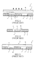
The manufacturing method of the embedded circuit board having the above configuration according to the preferred embodiment of the present invention will be described in more detail with reference to FIG. 8.
According to the manufacturing method of the embedded circuit board as shown in FIG. 8, the first CCL 20 formed with the plurality of cavities 21 is prepared in Step 1.
The plurality of chips 50 and 51 having different thicknesses are embedded in the cavities 21 in Step 2.
The adhesive portion 60 is provided on the upper surfaces of the chips 51 having thicknesses smaller than that of the first CCL 20 in Step 3.
The adhesive portion 60 is formed of epoxy or attach film.
The second CCL 30 adheres to the chips 51, on which the adhesive portion 60 is provided, to allow the chips 51 to level with the first CCL 20 in Step 4.
The RCC 40 coated with the resin 41 is laminated on the upper surfaces of the first and second CCLs 20 and 30 in Step 5.
The first and second CCLs 20 and 30 and the RCC 40 are subject to a heat compression process in Step 6.
The second CCL 30 is formed with the plurality of first via holes 31 through which the heat of the chips 51 is discharged.
The RCC 40 is formed with the plurality of second via holes 42 to discharge the heat through the first via holes 31 to the outside and to perform the EMI shield function.
The embedded circuit board and the manufacturing method thereof according to the invention as described above are not limited to the previous embodiment and the drawings. While the invention has been shown and described with reference to certain embodiments thereof, it will be understood by those skilled in the art that various changes in form and details may be made therein without departing from the spirit and scope of the invention as defined by the appended claims.

Claims (7)

What is claimed is:
1. A embedded circuit board comprising:
a first copper clad laminate formed with a plurality of cavities with a plurality of chips having different thicknesses embedded in the plurality of cavities;
a second copper clad laminate provided in the plurality of cavities to allow the first copper clad laminate to level with the plurality of chips; and
a resin coated copper foil provided on upper surfaces of the first and second copper clad laminates.
2. The embedded circuit board of claim 1, further comprising an adhesive portion provided on upper surfaces of the chips such to adhere the chips to the second copper clad laminate.
3. The embedded circuit board of claim 2, wherein the adhesive portion is formed of epoxy or attach film.
4. The embedded circuit board of claim 1, wherein the second copper clad laminate is formed with a plurality of first via holes to discharge heat generated by the plurality of chips.
5. The embedded circuit board of claim 1, wherein the resin coated copper foil is formed with a plurality of second via holes to discharge the heat through first via holes and perform an EMI shield function.
6. The embedded circuit board of claim 5, wherein the second via holes include ground via holes.
7. The embedded circuit board of claim 1, wherein the resin coated copper foil is coated with resin and heat-compressed to the first and second copper clad laminates after a lamination process.
US12/974,763 2009-12-24 2010-12-21 Embedded circuit board and manufacturing method thereof Active 2032-02-07 US8552302B2 (en)

Applications Claiming Priority (2)

Application Number Priority Date Filing Date Title
KR10-2009-0131024 2009-12-24
KR1020090131024A KR101677284B1 (en) 2009-12-24 2009-12-24 Embedded circuit board and manufacturing thereof

Publications (2)

Publication Number Publication Date
US20110155426A1 US20110155426A1 (en) 2011-06-30
US8552302B2 true US8552302B2 (en) 2013-10-08

Family

ID=44186067

Family Applications (1)

Application Number Title Priority Date Filing Date
US12/974,763 Active 2032-02-07 US8552302B2 (en) 2009-12-24 2010-12-21 Embedded circuit board and manufacturing method thereof

Country Status (2)

Country Link
US (1) US8552302B2 (en)
KR (1) KR101677284B1 (en)

Cited By (2)

* Cited by examiner, † Cited by third party
Publication number Priority date Publication date Assignee Title
US20130258623A1 (en) * 2012-03-29 2013-10-03 Unimicron Technology Corporation Package structure having embedded electronic element and fabrication method thereof
US10699985B2 (en) 2016-02-26 2020-06-30 Samsung Electronics Co., Ltd. Electronic device including cooling structure

Families Citing this family (3)

* Cited by examiner, † Cited by third party
Publication number Priority date Publication date Assignee Title
KR101976602B1 (en) * 2012-12-26 2019-05-10 엘지이노텍 주식회사 Printed circuit board and manufacturing method thereof
CN112838016B (en) * 2021-01-16 2023-04-28 北京工业大学 Chip thickening method for embedded substrate
CN116033645A (en) 2021-10-26 2023-04-28 奥特斯奥地利科技与系统技术有限公司 Coreless component carrier and method for producing a coreless component carrier

Citations (3)

* Cited by examiner, † Cited by third party
Publication number Priority date Publication date Assignee Title
US20080123308A1 (en) * 2004-09-15 2008-05-29 Samsung Electro-Mechanics Co., Ltd. Printed circuit board including embedded passive component and method of fabricating same
US20090139753A1 (en) * 2006-02-06 2009-06-04 Lg Chem, Ltd. Copper Clad Laminate for Chip on Film
US20100078204A1 (en) * 2008-09-29 2010-04-01 Samsung Electro-Mechanics Co., Ltd. Printed circuit board including electronic component embedded therein and method of manufacturing the same

Family Cites Families (2)

* Cited by examiner, † Cited by third party
Publication number Priority date Publication date Assignee Title
JP2004128002A (en) 2002-09-30 2004-04-22 Taiyo Yuden Co Ltd Electronic part built-in type multilayer substrate
JP4339739B2 (en) 2004-04-26 2009-10-07 太陽誘電株式会社 Multi-layer board with built-in components

Patent Citations (3)

* Cited by examiner, † Cited by third party
Publication number Priority date Publication date Assignee Title
US20080123308A1 (en) * 2004-09-15 2008-05-29 Samsung Electro-Mechanics Co., Ltd. Printed circuit board including embedded passive component and method of fabricating same
US20090139753A1 (en) * 2006-02-06 2009-06-04 Lg Chem, Ltd. Copper Clad Laminate for Chip on Film
US20100078204A1 (en) * 2008-09-29 2010-04-01 Samsung Electro-Mechanics Co., Ltd. Printed circuit board including electronic component embedded therein and method of manufacturing the same

Cited By (4)

* Cited by examiner, † Cited by third party
Publication number Priority date Publication date Assignee Title
US20130258623A1 (en) * 2012-03-29 2013-10-03 Unimicron Technology Corporation Package structure having embedded electronic element and fabrication method thereof
US10699985B2 (en) 2016-02-26 2020-06-30 Samsung Electronics Co., Ltd. Electronic device including cooling structure
US10957620B2 (en) 2016-02-26 2021-03-23 Samsung Electronics Co., Ltd. Electronic device including cooling structure
US12100637B2 (en) 2016-02-26 2024-09-24 Samsung Electronics Co., Ltd. Electronic device including cooling structure

Also Published As

Publication number Publication date
US20110155426A1 (en) 2011-06-30
KR101677284B1 (en) 2016-11-18
KR20110074138A (en) 2011-06-30

Similar Documents

Publication Publication Date Title
US7811626B2 (en) Printed circuit board and method of manufacturing the same
US20120227261A1 (en) Method for manufacturing printed wiring board
US8482117B2 (en) Semiconductor device with electronic component incorporation substrate
US20080006942A1 (en) Bottom substrate of package on package and manufacturing method thereof
US9439282B2 (en) Method for manufacturing printed circuit board
EP2854168A2 (en) Embedded semiconductor device package and method of manufacturing thereof
KR101143042B1 (en) Package substrate for mounting semiconductor element and method for manufacturing the package substrate
US8552302B2 (en) Embedded circuit board and manufacturing method thereof
TWI405511B (en) Printed circuit board with electronic components and method of manufacturing same
WO2007080713A1 (en) Printed wiring board with built-in semiconductor element, and process for producing the same
CN110636702B (en) Circuit board and manufacturing method thereof
CN103871996A (en) Package structure and manufacturing method thereof
US20060166490A1 (en) Forming buried via hole substrates
US20130139382A1 (en) Printed circuit board having electro component and manufacturing method thereof
JP5302920B2 (en) Manufacturing method of multilayer wiring board
KR101150036B1 (en) Active ic chip embedded multilayer flexible printed circuit board and method of manufacturing the same
KR101214357B1 (en) Semiconductor element-mounting package substrate, and method for manufacturing package substrate
US9865561B2 (en) Electronic package having a supporting board and package carrier thereof
US8603858B2 (en) Method for manufacturing a semiconductor package
KR20140078197A (en) Printed circuit board and manufacturing method thereof
US7562446B2 (en) Method for manufacturing substrate with cavity
US20070065986A1 (en) Method for manufacturing substrate with cavity
US9320148B2 (en) Printed wiring board
CN100553412C (en) Method for manufacturing module with built-in component and module with built-in component
EP3001783A1 (en) Component-embedded substrate and manufacturing method for same

Legal Events

Date Code Title Description
AS Assignment

Owner name: SAMSUNG ELECTRONICS CO., LTD., KOREA, REPUBLIC OF

Free format text: ASSIGNMENT OF ASSIGNORS INTEREST;ASSIGNORS:PARK, KYUNG-WAN;CHO, SHI-YUN;KIM, BYUNG-JIK;AND OTHERS;REEL/FRAME:025678/0312

Effective date: 20101220

STCF Information on status: patent grant

Free format text: PATENTED CASE

FEPP Fee payment procedure

Free format text: PAYOR NUMBER ASSIGNED (ORIGINAL EVENT CODE: ASPN); ENTITY STATUS OF PATENT OWNER: LARGE ENTITY

FPAY Fee payment

Year of fee payment: 4

MAFP Maintenance fee payment

Free format text: PAYMENT OF MAINTENANCE FEE, 8TH YEAR, LARGE ENTITY (ORIGINAL EVENT CODE: M1552); ENTITY STATUS OF PATENT OWNER: LARGE ENTITY

Year of fee payment: 8

MAFP Maintenance fee payment

Free format text: PAYMENT OF MAINTENANCE FEE, 12TH YEAR, LARGE ENTITY (ORIGINAL EVENT CODE: M1553); ENTITY STATUS OF PATENT OWNER: LARGE ENTITY

Year of fee payment: 12