US8516429B2 - Circuit optimization method and apparatus for analog circuit migration - Google Patents
Circuit optimization method and apparatus for analog circuit migration Download PDFInfo
- Publication number
- US8516429B2 US8516429B2 US13/640,594 US201113640594A US8516429B2 US 8516429 B2 US8516429 B2 US 8516429B2 US 201113640594 A US201113640594 A US 201113640594A US 8516429 B2 US8516429 B2 US 8516429B2
- Authority
- US
- United States
- Prior art keywords
- circuit
- direct current
- current path
- target
- devices
- Prior art date
- Legal status (The legal status is an assumption and is not a legal conclusion. Google has not performed a legal analysis and makes no representation as to the accuracy of the status listed.)
- Active
Links
Images


Classifications
-
- G—PHYSICS
- G06—COMPUTING OR CALCULATING; COUNTING
- G06F—ELECTRIC DIGITAL DATA PROCESSING
- G06F30/00—Computer-aided design [CAD]
- G06F30/30—Circuit design
- G06F30/36—Circuit design at the analogue level
- G06F30/367—Design verification, e.g. using simulation, simulation program with integrated circuit emphasis [SPICE], direct methods or relaxation methods
Definitions
- the present disclosure relates to design automation of an integrated circuit, and in particular, to an optimization method and an optimization apparatus for analog circuit migration.
- the design of a digital integrated circuit is highly automated and the design period of the digital integrated circuit is thus greatly reduced.
- the design of an analog integrated circuit is mostly manual. Consequently, the design period of the analog integrated circuit is typically 2 or 3 times that of the digital integrated circuit.
- the design period of a hybrid integrated circuit is limited by the design period of the analog integrated circuit.
- the design period of the analog integrated circuit can be reduced by increasing the design automation of the analog integrated circuit.
- the design period of the hybrid integrated circuit can also be reduced.
- the design automation of the analog integrated circuit will lower the design cost and provide more competitive products.
- Analog circuit migration is typically used in the design of the analog integrated circuit, which migrates a source circuit to a target circuit.
- the analog circuit migration typically includes optimization of parameter values of devices of an integrated circuit in a circuit level and physical optimization of positions and wirings of the devices of the integrated circuit in a layout level.
- the first approach of circuit optimization includes the following work of a designer: setting parameter values of devices in accordance with prior knowledge, performing circuit simulation, and checking whether the design meets the design requirement or not. The steps of setting the parameter values, performing the circuit simulation and checking the design are repeated until properties of a target circuit approximates properties of a source circuit.
- the first approach of circuit optimization has the drawback that the optimization efficiency mainly relies on the designer's experience in designing the integrated circuit.
- the designer should well know variation of the performances of the circuit due to changes of the parameter values of the devices. Actually, the designer cannot well know the variation of the properties of the circuit due to the changes of the parameter values of the devices, when a scale and an integration level of the integrated circuit are increased. The design efficiency of the above approach will be very low.
- the second approach of circuit optimization includes scanning parameter values of the devices and performing circuit simulation using a circuit simulator, and setting suitable parameter values of the devices in accordance with a result of the circuit simulation.
- the second approach is typically supplementary to the first approach.
- the second approach of circuit optimization has the drawback that only a limited number of parameters can be scanned. The designer needs to manually select the parameters to be scanned, determine a sequence of scanning the parameters, and set parameter values in accordance with the result of simulation. It is more and more difficult for the designer to manually select the parameters to be scanned, determine a sequence of scanning the parameters, and set parameter values, when the scale and the integration level of the integrated circuit are increased.
- the third approach of circuit optimization includes randomly setting parameter values of the devices, performing circuit simulation or symbolic analysis to obtain performances of the circuit, controlling an optimization process globally to obtain optimal parameter values by optimization algorithm such as simulated annealing, genetic algorithm, and Particle Swarm Optimization (PSO), etc.
- the third approach of circuit optimization has the drawback that computational complexity is too large to be used in the circuit optimization of the analog integrated circuit with a large scale and a large complexity.
- An object of the present disclosure is to provide an optimization method and an optimization apparatus for analog circuit migration with increased optimization efficiency.
- a circuit optimization method used in analog circuit migration which migrates a source circuit to a target circuit, comprising: dividing the source circuit into at least one direct current path; determining an adaptation sequence of the at least one direct current path; and optimizing the at least one direct current path in the target circuit one by one in the adaptation sequence.
- a circuit optimization apparatus used in analog circuit migration which migrates a source circuit to a target circuit, comprising: a circuit simulation unit configured to perform source circuit simulation and target circuit simulation; a circuit simulation result analyzing unit coupled to the circuit simulation unit and configured to calculate node signals of the source circuit and the target circuit in accordance with results of the source circuit simulation and the target circuit simulation; a circuit connection analyzing unit coupled to the circuit simulation result analyzing unit and configured to analyzing circuit connections of the source circuit to determine direct current paths in the source circuit; a circuit adaptation sequence determining unit coupled to the circuit connection analyzing unit and configured to analyze a signal arrival sequence of the direct current paths in the source circuit and obtain an adaptation sequence of the direct current paths in the source circuit in accordance with the signal arrival sequence; a parameter value setting unit coupled to the circuit simulation unit and an optimization control unit, and configured to setting parameter values of the devices in one of the direct current path in the target circuit; a signal comparison unit coupled to the circuit simulation result analyzing unit, and configured to compare node signals of
- the circuit optimization method and the circuit optimization apparatus divide the source circuit into at least one direct current path, utilize the at least one direct current path as elements of the circuit optimization, and perform the circuit optimization on the at least one direct current path one by one in the adaptation sequence.
- the performances of the target circuit match with those of the source circuit at nodes of the direct current paths one by one in the circuit optimization of the analog circuit migration. It ensures that external terminals of the target circuit in new manufacture process meet the requirements of the performance of the target circuit. Moreover, the circuit optimization method and the circuit optimization apparatus decrease computational complexity and the number of invalid trials in the optimization process. It increases the design efficiency in the circuit optimization of the analog circuit migration.
- FIG. 1 is a flow chart illustrating a circuit optimization method used in analog circuit migration according to an embodiment of the present disclosure
- FIG. 2 is a block diagram illustrating how to analyze electrical connections in the circuit optimization method used in the analog circuit migration according to an embodiment of the present disclosure
- FIG. 3 is a flow chart illustrating an optimization control in the circuit optimization method used in the analog circuit migration according to an embodiment of the present disclosure.
- FIG. 4 is a block diagram illustrating a circuit optimization apparatus used in analog circuit migration according to an embodiment of the present disclosure.
- the term “external terminal” means input/output terminals of the source/target circuit as a while for connecting with external circuits;
- the term “node” means joints of different parts of the source/target circuit, such as joints between devices or between module;
- the term “signal branch” means a signal path through devices between one node and another node in the source/target circuit;
- the term “direct current path” means a path of direct current traversing devices between a voltage supply terminal and a ground terminal;
- the terminal “signal arrival sequence” means a sequence that a signal arrives different modules, different direct current paths, or different devices, in a direction of signal propagation. For example, the signal firstly arrives an input terminal and finally arrives an output terminal.
- the source circuit and the target circuit each comprise a plurality of devices connected between a plurality of nodes.
- the source circuit and the target circuit each can be divided into at least one module, such as a power supply module, a receiver module, an amplification module, and a signal processing module, etc.
- Each module includes some devices. Different modules are connected to each other at nodes between the modules, and different devices are connected to each other at the nodes in the modules or between the modules.
- the inventor recognizes that the prior approaches of circuit optimization have the above drawbacks mainly because the properties at the external terminals of the source circuit are seen as optimization criteria in the circuit optimization of the circuit migration while the properties at the nodes of the source circuit are omitted. However, it is the properties at the nodes of the source circuit which ensure the properties at the external terminals of the source circuit. Thus, the computational complexity can be decreased by taking the properties at the nodes of the source circuit as the optimization criteria.
- FIG. 1 is a flow chart illustrating a circuit optimization method used in analog circuit migration according to an embodiment of the present disclosure.
- step S 101 source circuit simulation is performed in step S 101 .
- Circuit simulation tools commercially available, such as Spectre from Cadence Inc and Hspice from Synopsys Inc., can be used in the source circuit simulation.
- the source circuit simulation includes direct current (DC) analysis, alternating current (AC) analysis, transient analysis and other numerical analysis on the whole source circuit. Details of the above analysis technologies can be read in those published textbooks and documents, and thus not described here.
- a result of the source circuit simulation is then analyzed in step S 102 .
- the analysis include calculating signal values/profile and functional representation in DC analysis, signal values/profile and functional representation in AC analysis, and signal values/profile and functional representation in transient analysis at different nodes and braches, from the result of the source circuit simulation.
- An object or a range of the source circuit simulation includes voltages at all nodes, and currents at all branches in the source circuit, and functional representation of the above parameters.
- the analysis includes direct current path analysis and signal flow (including feedback paths) analysis.
- the source circuit can be divided into circuit module 1 , circuit module 2 , circuit module 3 , circuit module 4 , circuit module 5 , circuit module 6 , . . . , and circuit module N m , as shown in FIG. 2 .
- devices in each circuit module are traversed from any voltage supply terminal to any ground terminal of the circuit module in a direction that current flows in the circuit module.
- the current flows from a drain to a source in a MOS transistor, from a collector to an emitter in a bipolar transistor, from one terminal to the other terminal in a resistor, and from a P-type region to an N-type region in a diode.
- the devices which are connected between the same voltage supply terminal and the same ground terminal, constitute a direct current path.
- At least one direct current path can be obtained in each circuit module.
- the circuit module 4 in FIG. 2 can be subdivided into direct current path 1 , direct current path 2 , direct current path 3 , direct current path 4 , direct current path 5 , direct current path 6 , . . . , and direct current path N p .
- each direct current path known from the direct current path analysis is seen as a unit.
- the direct current path is an element of each circuit module.
- all of the direct current paths are traversed from an input terminal to an output terminal in a direction of single propagation.
- An arrival sequence of the signal in the direction of the signal propagation can be denoted by a signal depth. For example, if the current direct current path has the signal depth N, the next direct current path in the direction of the signal propagation has the signal dept N+1.
- An adaptation sequence of the circuit is then determined in step S 104 .
- the adaptation sequence of the circuit modules and the direct current paths can be determined in accordance with the arrival sequence of the signal.
- the adaptation sequence of the circuit modules in FIG. 2 is circuit module 1 , circuit module 2 , circuit module 3 , circuit module 4 , circuit module 5 , circuit module 6 , . . . , and circuit module N m .
- the adaptation sequence of the direct current paths in circuit module 4 is direct current path 1 , direct current path 2 , direct current path 3 , direct current path 4 , direct current path 5 , direct current path 6 , . . . , and direct current path N p .
- Parameter values of the devices in the target circuit are then set for each direct current path in step S 105 . It includes setting initial parameter values of the devices in the circuit and setting intermediate parameter values of the devices in the optimization of the parameter values of the devices.
- the initial parameter values of the devices in the target circuit can be set by
- the method a) can be easily implemented.
- the initial parameter value if being randomly set, is uncertain. It may deviate largely from the final optimal value and require a large number of iterations in the subsequent optimization.
- the method b) seems to be more complex than the method a).
- the method b) provides an initial parameter value close to the final optimal value, and requires a less number of iterations. Thus, optimization efficiency of the method b) is higher than that of the method a).
- the intermediate parameter values of the devices in the target circuit can be set by
- Pi old is an unadjusted value of parameter Pi of the i-th device
- fspec is target property of the target circuit
- fmeas is actual property of the target circuit when the value of the parameter Pi of the i-th device has a parameter value Pi old ;
- k is a factor representing an effect of the value of the parameter Pi of the i-th device on the property of the target circuit; when k is equal to 0, the value of Pi is constant.
- the intermediate parameter values of the devices in the target circuit can be determined for one major circuit property.
- fspec j is the j-th target property of the target circuit
- fcalc j is the j-th actual property of the target circuit when the value of the parameter Pi of the i-th device has a parameter value Pi new ;
- K j is a factor representing an effect of the value of the parameter Pi of the i-th device on the j-th property of the target circuit; when k j is equal to 0, the value of Pi is constant.
- the method a) can be easily implemented.
- the intermediate parameter value if being randomly set, is uncertain.
- the change of the parameter value may occur in a wrong tendency to cause invalid trials.
- Even in a case that the changed of the parameter value occurs in a correct tendency the parameter value may be far away from the optimal parameter value, and require a large number of iterations in the subsequent optimization.
- the method b) seems to be more complex than the method a).
- the method b) provides an intermediate parameter value close to the final optimal value in a correct tendency, and requires a less number of iterations.
- the optimization efficiency of the method b) is higher than that of the method a).
- Target circuit simulation is then performed in step S 106 , and a result of the target circuit simulation is analyzed in step S 107 .
- the target circuit simulation in step S 106 may use a simulation tool similar to that used in the source circuit simulation in step S 101 , and the result of the target circuit simulation may also be analyzed in a similar manner, details of which are omitted here.
- the target circuit simulation is performed on an object and a range different from those in the source circuit simulation.
- a direct current path is used as an element of circuit optimization in the present disclosure.
- the object of the target circuit simulation is one direct current path of the target circuit.
- the direct current paths of the target circuit are optimized one by one in the adaptation sequence determined in step S 104 .
- the first object of the target circuit simulation is the first direct current path in the first circuit module
- the second object of the target circuit simulation is the second direct current path of the first circuit module, etc.
- a range of the target circuit simulation includes voltages at all nodes and currents at all branches in the current direct current path and the direct current paths before the current direct current path in the target circuit, and functional representation of the above parameters.
- Signals at corresponding nodes of the source circuit and the target circuit are compared in step S 108 .
- a direct current path is used as an element of circuit optimization in the present disclosure.
- the comparison here includes comparing corresponding voltages at all nodes and corresponding currents at all branches in the current direct current path and the direct current paths before the current direct current path in the source circuit and the target circuit, and comparing corresponding functional representation of the above parameters.
- step S 109 It is then determined whether circuit property of the target circuit meets the design requirement in step S 109 .
- the circuit optimization is ended in step S 110 , if the target circuit meets the design requirement. Otherwise, that is the target circuit does not meet the design requirement, the process turns to step S 105 .
- the operations in steps S 105 -S 109 are repeated while setting new parameter values of the devices in the target circuit and/or selecting next one of the direct current paths in the target circuit as a new object of circuit simulation.
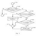
- FIG. 3 is a flow chart illustrating an optimization control in the circuit optimization method used in the analog circuit migration according to an embodiment of the present disclosure.
- the optimization criteria are involved in step S 109 .
- step S 10901 it is determined whether a result of global optimization of the target circuit meets the design requirement. If yes, the process turns to step S 110 to end the circuit optimization. If no, the process turns to step S 10902 to continue subsequent operations.
- step S 10902 it is determined whether the current direct current path in the target circuit meets the design requirement. If yes, the process turns to step S 10903 to select next one of the direct current paths in the target circuit as a new object of circuit simulation, and further to step S 105 to repeat the operations at steps S 105 -S 109 , to set initial parameter values of the devices in the next one of the direct current paths in the target circuit. If no, the process turns to step S 10904 to continue subsequent operations.
- step S 10904 it is determined whether the number of iterations for optimizing the current direct current path in the target circuit is larger than a maximum at a simulated annealing temperature or in a genetic generation. If yes, the process turns to step S 10905 to change the simulated annealing temperature and/or the genetic generation, and further to step S 105 to repeat the operations at steps S 105 -S 109 , to optimize the parameter values of the devices in the current direct current path in the target circuit at new simulated annealing temperature and/or new genetic generation. If no, the process turns to step S 105 to repeat the operations at steps S 105 -S 109 , to set new parameter values of the devices in the current direct current path in the target circuit.
- the direct current paths in the target circuit are optimized one by one in the adaptation sequence which is determined on the basis of the analysis result of the source circuit. Because the last direct current path in the previous one circuit module is always followed by the first direct current path in the next one circuit module, the circuit modules of the target circuit are also optimized one by one.
- the circuit optimization method used in the analog circuit migration is described above, in which the source circuit and the target circuit are divided into the corresponding circuit modules, which are subdivided into the corresponding direct current paths in each of the circuit modules.
- the source circuit and the target circuit may be divided directly into some direct current paths, without firstly being divided into circuit modules.
- the source circuit and the target circuit may be each analyzed as a whole in a case that the integrated circuit has a small size or complex feedback paths, because the optimization efficiency will be increased.
- FIG. 4 is a block diagram illustrating a circuit optimization apparatus used in analog circuit migration according to an embodiment of the present disclosure.
- the circuit optimization apparatus comprises a circuit simulation unit U 101 , a circuit simulation result analyzing unit U 102 , a circuit connection analyzing unit U 103 , a circuit adaptation sequence determining unit U 104 , a parameter value setting unit U 105 , a signal comparison unit U 106 , and an optimization control unit U 107 .
- Each unit of the circuit optimization apparatus may be in the form of hardware, software, firmware, or any combination thereof.
- the circuit simulation unit U 101 carries out direct current (DC) analysis, alternating current (AC) analysis, transient analysis and other numerical analysis on each of the source circuit and the target circuit.
- DC direct current
- AC alternating current
- transient analysis and other numerical analysis on each of the source circuit and the target circuit.
- the circuit simulation result analyzing unit U 102 is coupled to the circuit simulation unit U 101 .
- the circuit simulation result analyzing unit U 102 calculates signal values/profile and functional representation in DC analysis, signal values/profile and functional representation in AC analysis, and signal values/profile and functional representation in transient analysis at corresponding nodes and braches of the source circuit and the target circuit, from the result of circuit simulation of the source circuit and the target circuit.
- the circuit simulation of the source circuit and the target circuit are both performed in the circuit simulation unit U 101
- the analysis of the result of the circuit simulation of the source circuit and the target circuit are both performed in the circuit simulation result analyzing unit U 102 .
- an object and a range of the circuit simulation of the source circuit is different from an object and a range of the circuit simulation of the target circuit.
- the object or the range of the source circuit simulation includes voltages at all nodes, and currents at all branches in the source circuit, and functional representation of the above parameters.
- the present disclosure utilizes the direct current paths as elements of the circuit optimization.
- the object of the circuit simulation of the target circuit is a direct current path.
- the direct current paths of the target circuit are optimized one by one in the adaptation sequence.
- the first object of the target circuit simulation is the first direct current path in the first circuit module
- the second object of the target circuit simulation is the second direct current path of the first circuit module
- a range of the target circuit simulation includes voltages at all nodes and currents at all branches in the current direct current path and the direct current paths before the current direct current path in the target circuit, and functional representation of the above parameters.
- the circuit connection analyzing unit U 103 is coupled to the circuit simulation result analyzing unit U 102 .
- the circuit connection analyzing unit U 103 analyzes electrical connects of devices in the source circuit by traversing the devices in the source circuit from any voltage supply terminal to any ground terminal of the source circuit in a direction that current flows in the source circuit.
- the circuit adaptation sequence determining unit U 104 is coupled to the circuit connection analyzing unit U 103 .
- the circuit adaptation sequence determining unit U 104 analyzes a signal arrival sequence of the direct current paths in the source circuit by traversing all of the direct current paths from an input terminal to an output terminal in a direction of single propagation. An adaptation sequence of the circuit modules and the direct current paths is determined in accordance with the signal arrival sequence.
- the parameter value setting unit U 105 is coupled to the circuit simulation unit U 101 and an optimization control unit U 107 .
- the parameter value setting unit U 105 sets initial parameter values of the devices in the target circuit for the circuit simulation unit U 101 , and sets intermediate parameter values of the devices in the target circuit for the circuit simulation unit U 101 in the circuit optimization in accordance with a control signal of the optimization control unit U 107 .
- the signal comparison unit U 106 is coupled to the circuit simulation result analyzing unit U 102 .
- the signal comparison unit U 106 compares corresponding voltages at all nodes and corresponding currents at all branches in the current direct current path and the direct current paths before the current direct current path in the source circuit and the target circuit, and compares corresponding functional representation of the above parameters.
- the optimization control unit U 107 is coupled to the signal comparison unit U 106 and the parameter value setting unit U 105 .
- the optimization unit U 107 provides a control signal to the parameter value setting unit U 105 in accordance with a comparison result of the signal comparison unit U 106 to optimize the direct current paths in the target circuit one by one in the adaptation sequence.
- the parameter value setting unit U 105 either sets intermediate parameter values of the devices in the current direct current path in the target circuit for new circuit optimization trials, or sets initial parameter values of the devices in the next one direct current path in the target circuit.
- the optimization unit U 107 varies a simulated annealing temperature and/or a genetic generation for new circuit optimization trials, if a number of invalid trials is larger than a maximum in the simulated annealing temperature and/or the genetic generation. After completing circuit optimization of all of the direct current paths in the target circuit (that is, electrical properties of the target circuit meet the design requirement), the optimization control unit U 107 ends the circuit optimization process.
- the above circuit optimization method apparatus utilize the direct current paths as elements of the circuit optimization, which decreases computational complexity and the number of invalid trials in the optimization process.
- an object and a range of optimization is the same in a target circuit as in a source circuit, including voltages at all nodes, and currents at all branches in the target circuit, and functional representation of the above parameters.
- the source circuit comprises 50 devices, each with an exploration space of 8.
- An exploration space of the source circuit as a whole will be 8 50 .
- T 1 is a time period for one optimization trial.
- the circuit optimization method performs direct current path analysis and signal flow analysis to obtain devices in each of direct current paths, determine an adaptation sequence of the direct current paths in the optimization process, and optimize the direct current paths in the target circuit one by one in the adaptation sequence.
- the source circuit also comprises 50 devices, each with an exploration space of 8. Further, in the example, the source circuit can be divided into 10 direct current paths, each with 5 devices. An exploration space of one direct current path will be 8 5 . Thus, the hit probability in each iteration of the optimization process is 1 ⁇ 8 5 .
- An actual optimization trial time T all of the target circuit can be represented by
- T part, i is an actual optimization time for the i-th direct current path
- T 1 is a time period for one optimization trial.
Landscapes
- Engineering & Computer Science (AREA)
- Computer Hardware Design (AREA)
- Physics & Mathematics (AREA)
- Theoretical Computer Science (AREA)
- Microelectronics & Electronic Packaging (AREA)
- Evolutionary Computation (AREA)
- Geometry (AREA)
- General Engineering & Computer Science (AREA)
- General Physics & Mathematics (AREA)
- Design And Manufacture Of Integrated Circuits (AREA)
Abstract
Description
Pi new =Pi old+(fspec−fmeas)*k (1)
min(Σ(fspecj −fcalcj)2) (2)
wherein,
fcalcj =fmeas+k j*(Pi new −Pi old) (3)
T all =T 1×850 (4)
Claims (12)
Applications Claiming Priority (1)
| Application Number | Priority Date | Filing Date | Title |
|---|---|---|---|
| PCT/CN2011/082184 WO2013071480A1 (en) | 2011-11-15 | 2011-11-15 | Circuit optimization method and device for analog circuit transplantation |
Publications (2)
| Publication Number | Publication Date |
|---|---|
| US20130125080A1 US20130125080A1 (en) | 2013-05-16 |
| US8516429B2 true US8516429B2 (en) | 2013-08-20 |
Family
ID=48281911
Family Applications (1)
| Application Number | Title | Priority Date | Filing Date |
|---|---|---|---|
| US13/640,594 Active US8516429B2 (en) | 2011-11-15 | 2011-11-15 | Circuit optimization method and apparatus for analog circuit migration |
Country Status (2)
| Country | Link |
|---|---|
| US (1) | US8516429B2 (en) |
| WO (1) | WO2013071480A1 (en) |
Cited By (5)
| Publication number | Priority date | Publication date | Assignee | Title |
|---|---|---|---|---|
| US8710847B2 (en) | 2010-10-28 | 2014-04-29 | Donald Marvin | Self-correcting amplifier system |
| US8738310B2 (en) | 2010-12-08 | 2014-05-27 | Paul Swanton | Automatic determination of baselines for battery testing |
| US9030173B2 (en) | 2006-07-18 | 2015-05-12 | Global Energy Innovations, Inc. | Identifying and amerliorating a deteriorating condition for battery networks in-situ |
| US20240427977A1 (en) * | 2022-04-25 | 2024-12-26 | Faraday Dynamics. Ltd. | Quick simulation and optimization method and system for analog circuits |
| US12571851B2 (en) | 2020-03-25 | 2026-03-10 | Cadex Electronics Inc. | Apparatus and methods for testing electrochemical systems |
Families Citing this family (2)
| Publication number | Priority date | Publication date | Assignee | Title |
|---|---|---|---|---|
| CN103530484B (en) * | 2013-11-04 | 2016-05-04 | 中国科学院微电子研究所 | A device parameter optimization method for an integrated circuit |
| CN116029251B (en) * | 2023-03-23 | 2023-07-07 | 青岛青软晶尊微电子科技有限公司 | Circuit wiring optimization method and device based on circuit performance equalization |
Citations (8)
| Publication number | Priority date | Publication date | Assignee | Title |
|---|---|---|---|---|
| JP2001267324A (en) | 2000-03-22 | 2001-09-28 | Hitachi Ltd | Wiring correction method |
| CN1510733A (en) | 2002-12-24 | 2004-07-07 | 北京艾克赛利微电子技术有限公司 | Transistor integrated circuit optimization method for process transplantation |
| US20080134109A1 (en) * | 2005-09-29 | 2008-06-05 | Hammouda Sherif Ahmed Abdel-Wa | Analog Design Retargeting |
| US7659751B2 (en) | 2004-06-28 | 2010-02-09 | Technion Research & Development Foundation Ltd. | Multiple-output transistor logic circuit |
| US20100169848A1 (en) * | 2008-12-30 | 2010-07-01 | Danniel Nahmanny | Method of Migrating Electronic Devices Operating in Current Mode to a Target Technology |
| US7761820B2 (en) * | 2005-08-05 | 2010-07-20 | International Business Machines Corporation | Automated migration of analog and mixed-signal VLSI design |
| CN102024067A (en) | 2009-09-09 | 2011-04-20 | 中国科学院微电子研究所 | A method for analog circuit process transplantation |
| CN102508977A (en) | 2011-11-15 | 2012-06-20 | 中国科学院微电子研究所 | Circuit optimization method and device for analog circuit transplantation |
-
2011
- 2011-11-15 WO PCT/CN2011/082184 patent/WO2013071480A1/en not_active Ceased
- 2011-11-15 US US13/640,594 patent/US8516429B2/en active Active
Patent Citations (8)
| Publication number | Priority date | Publication date | Assignee | Title |
|---|---|---|---|---|
| JP2001267324A (en) | 2000-03-22 | 2001-09-28 | Hitachi Ltd | Wiring correction method |
| CN1510733A (en) | 2002-12-24 | 2004-07-07 | 北京艾克赛利微电子技术有限公司 | Transistor integrated circuit optimization method for process transplantation |
| US7659751B2 (en) | 2004-06-28 | 2010-02-09 | Technion Research & Development Foundation Ltd. | Multiple-output transistor logic circuit |
| US7761820B2 (en) * | 2005-08-05 | 2010-07-20 | International Business Machines Corporation | Automated migration of analog and mixed-signal VLSI design |
| US20080134109A1 (en) * | 2005-09-29 | 2008-06-05 | Hammouda Sherif Ahmed Abdel-Wa | Analog Design Retargeting |
| US20100169848A1 (en) * | 2008-12-30 | 2010-07-01 | Danniel Nahmanny | Method of Migrating Electronic Devices Operating in Current Mode to a Target Technology |
| CN102024067A (en) | 2009-09-09 | 2011-04-20 | 中国科学院微电子研究所 | A method for analog circuit process transplantation |
| CN102508977A (en) | 2011-11-15 | 2012-06-20 | 中国科学院微电子研究所 | Circuit optimization method and device for analog circuit transplantation |
Non-Patent Citations (2)
| Title |
|---|
| Search Report (PCT/ISA/210) from corresponding Application No. PCT/CN2011/082184, dated Aug. 30, 2012. |
| Written Opinion (PCT/ISA/237) from corresponding Application No. PCT/CN2011/082184, dated Aug. 13, 2012. |
Cited By (6)
| Publication number | Priority date | Publication date | Assignee | Title |
|---|---|---|---|---|
| US9030173B2 (en) | 2006-07-18 | 2015-05-12 | Global Energy Innovations, Inc. | Identifying and amerliorating a deteriorating condition for battery networks in-situ |
| US8710847B2 (en) | 2010-10-28 | 2014-04-29 | Donald Marvin | Self-correcting amplifier system |
| US8738310B2 (en) | 2010-12-08 | 2014-05-27 | Paul Swanton | Automatic determination of baselines for battery testing |
| US12571851B2 (en) | 2020-03-25 | 2026-03-10 | Cadex Electronics Inc. | Apparatus and methods for testing electrochemical systems |
| US20240427977A1 (en) * | 2022-04-25 | 2024-12-26 | Faraday Dynamics. Ltd. | Quick simulation and optimization method and system for analog circuits |
| US12197839B1 (en) * | 2022-04-25 | 2025-01-14 | Faraday Dynamics. Ltd. | Quick simulation and optimization method and system for analog circuits |
Also Published As
| Publication number | Publication date |
|---|---|
| US20130125080A1 (en) | 2013-05-16 |
| WO2013071480A1 (en) | 2013-05-23 |
Similar Documents
| Publication | Publication Date | Title |
|---|---|---|
| US8516429B2 (en) | Circuit optimization method and apparatus for analog circuit migration | |
| CN109117528B (en) | MOS device subcircuit temperature model based on BSIM4 model and modeling method | |
| US7761275B2 (en) | Synthesizing current source driver model for analysis of cell characteristics | |
| CN104376138B (en) | The time sequence determination method and device of IC chip | |
| US10108770B2 (en) | Corner process for analog circuit design optimization | |
| CN102508977B (en) | Circuit optimization method and device for analog circuit transplantation | |
| Lu et al. | Automatic op-amp generation from specification to layout | |
| US7281223B2 (en) | System and method for modeling an integrated circuit system | |
| US9898566B2 (en) | Method for automated assistance to design nonlinear analog circuit with transient solver | |
| US7240304B2 (en) | Method for voltage drop analysis in integreted circuits | |
| TWI716079B (en) | Simulation method for use in functional equivalence check | |
| CN114330192A (en) | GaN HEMT transistor small signal model modeling method | |
| US20250217566A1 (en) | System and method utilizing machine learning (ml) for analog and mixed-signal circuit layout synthesis | |
| CN119227499A (en) | Modeling method for IGBT switching transients in electric drive systems of new energy vehicles | |
| CN101329693A (en) | Method for modeling MOS tube resistor | |
| Rocha et al. | A new metaheuristc combining gradient models with NSGA-II to enhance analog IC synthesis | |
| Jarnda | Genetic algorithm based extraction method for distributed small-signal model of GaN HEMTs | |
| Ferdowsi et al. | A hybrid delay model for interconnected multi-input gates | |
| Sridhar et al. | An Adaptive Multi-Objective Optimization on CMOS Two Stage Op-Amp Circuit Synthesis | |
| WO2014077671A1 (en) | A method of generating spice-compatible isfet model | |
| CN105512439B (en) | Analogy decode circuit design method and system | |
| JP4413097B2 (en) | Delay time calculation method | |
| CN119783614B (en) | A Modeling and Application Method for Nonlinear Capacitance Model of DSRD Device | |
| JP2004319828A (en) | Circuit simulation method and semiconductor integrated circuit device | |
| CN117852475A (en) | Electromagnetic reliability prediction method for CMOS inverter based on neural network |
Legal Events
| Date | Code | Title | Description |
|---|---|---|---|
| AS | Assignment |
Owner name: INSTITUTE OF MICROELECTRONICS, CHINESE ACADEMY OF Free format text: ASSIGNMENT OF ASSIGNORS INTEREST;ASSIGNORS:WU, YUPING;CHEN, LAN;REEL/FRAME:029112/0923 Effective date: 20120626 |
|
| STCF | Information on status: patent grant |
Free format text: PATENTED CASE |
|
| CC | Certificate of correction | ||
| FPAY | Fee payment |
Year of fee payment: 4 |
|
| MAFP | Maintenance fee payment |
Free format text: PAYMENT OF MAINTENANCE FEE, 8TH YR, SMALL ENTITY (ORIGINAL EVENT CODE: M2552); ENTITY STATUS OF PATENT OWNER: SMALL ENTITY Year of fee payment: 8 |
|
| MAFP | Maintenance fee payment |
Free format text: PAYMENT OF MAINTENANCE FEE, 12TH YR, SMALL ENTITY (ORIGINAL EVENT CODE: M2553); ENTITY STATUS OF PATENT OWNER: SMALL ENTITY Year of fee payment: 12 |