US8501332B2 - Energy conversion cell having a dielectrically graded region to alter transport, and methods thereof - Google Patents
Energy conversion cell having a dielectrically graded region to alter transport, and methods thereof Download PDFInfo
- Publication number
- US8501332B2 US8501332B2 US12/701,272 US70127210A US8501332B2 US 8501332 B2 US8501332 B2 US 8501332B2 US 70127210 A US70127210 A US 70127210A US 8501332 B2 US8501332 B2 US 8501332B2
- Authority
- US
- United States
- Prior art keywords
- region
- energy conversion
- conversion cell
- transport
- dielectric
- Prior art date
- Legal status (The legal status is an assumption and is not a legal conclusion. Google has not performed a legal analysis and makes no representation as to the accuracy of the status listed.)
- Expired - Fee Related, expires
Links
- 238000006243 chemical reaction Methods 0.000 title claims abstract description 197
- 238000000034 method Methods 0.000 title abstract description 22
- 239000000446 fuel Substances 0.000 claims abstract description 18
- 239000000463 material Substances 0.000 claims description 62
- 239000002245 particle Substances 0.000 claims description 57
- 239000011159 matrix material Substances 0.000 claims description 45
- 230000005684 electric field Effects 0.000 claims description 36
- 150000002500 ions Chemical class 0.000 claims description 33
- 239000002131 composite material Substances 0.000 claims description 23
- 230000004048 modification Effects 0.000 claims description 21
- 238000012986 modification Methods 0.000 claims description 21
- 230000003595 spectral effect Effects 0.000 claims description 21
- 239000003989 dielectric material Substances 0.000 claims description 19
- 238000010521 absorption reaction Methods 0.000 claims description 15
- 239000007788 liquid Substances 0.000 claims description 15
- 239000007787 solid Substances 0.000 claims description 14
- 239000004065 semiconductor Substances 0.000 claims description 12
- -1 exciton Chemical class 0.000 claims description 8
- 239000000203 mixture Substances 0.000 claims description 6
- 229920000642 polymer Polymers 0.000 claims description 6
- XLYOFNOQVPJJNP-UHFFFAOYSA-N water Substances O XLYOFNOQVPJJNP-UHFFFAOYSA-N 0.000 claims description 6
- 239000003054 catalyst Substances 0.000 claims description 5
- 229920003023 plastic Polymers 0.000 claims description 5
- 239000004033 plastic Substances 0.000 claims description 5
- 239000011856 silicon-based particle Substances 0.000 claims description 5
- 239000000126 substance Substances 0.000 abstract description 8
- 230000032258 transport Effects 0.000 description 143
- 210000004027 cell Anatomy 0.000 description 137
- 241000894007 species Species 0.000 description 58
- 238000005516 engineering process Methods 0.000 description 28
- 230000037230 mobility Effects 0.000 description 21
- GWEVSGVZZGPLCZ-UHFFFAOYSA-N Titan oxide Chemical compound O=[Ti]=O GWEVSGVZZGPLCZ-UHFFFAOYSA-N 0.000 description 17
- 239000000975 dye Substances 0.000 description 12
- XLOMVQKBTHCTTD-UHFFFAOYSA-N Zinc monoxide Chemical compound [Zn]=O XLOMVQKBTHCTTD-UHFFFAOYSA-N 0.000 description 8
- 230000000694 effects Effects 0.000 description 8
- 230000008901 benefit Effects 0.000 description 7
- 230000008859 change Effects 0.000 description 7
- 230000033001 locomotion Effects 0.000 description 7
- 238000009792 diffusion process Methods 0.000 description 6
- 239000011521 glass Substances 0.000 description 6
- 229910021417 amorphous silicon Inorganic materials 0.000 description 5
- 238000010348 incorporation Methods 0.000 description 5
- 229910021421 monocrystalline silicon Inorganic materials 0.000 description 5
- OGIDPMRJRNCKJF-UHFFFAOYSA-N titanium oxide Inorganic materials [Ti]=O OGIDPMRJRNCKJF-UHFFFAOYSA-N 0.000 description 5
- UFHFLCQGNIYNRP-UHFFFAOYSA-N Hydrogen Chemical compound [H][H] UFHFLCQGNIYNRP-UHFFFAOYSA-N 0.000 description 4
- 229930002877 anthocyanin Natural products 0.000 description 4
- 235000010208 anthocyanin Nutrition 0.000 description 4
- 239000004410 anthocyanin Substances 0.000 description 4
- 150000004636 anthocyanins Chemical class 0.000 description 4
- 238000000576 coating method Methods 0.000 description 4
- 239000001257 hydrogen Substances 0.000 description 4
- 229910052739 hydrogen Inorganic materials 0.000 description 4
- 230000002401 inhibitory effect Effects 0.000 description 4
- 230000010287 polarization Effects 0.000 description 4
- 238000012546 transfer Methods 0.000 description 4
- 239000011787 zinc oxide Substances 0.000 description 4
- XUIMIQQOPSSXEZ-UHFFFAOYSA-N Silicon Chemical compound [Si] XUIMIQQOPSSXEZ-UHFFFAOYSA-N 0.000 description 3
- 239000006096 absorbing agent Substances 0.000 description 3
- PNEYBMLMFCGWSK-UHFFFAOYSA-N aluminium oxide Inorganic materials [O-2].[O-2].[O-2].[Al+3].[Al+3] PNEYBMLMFCGWSK-UHFFFAOYSA-N 0.000 description 3
- 239000000969 carrier Substances 0.000 description 3
- 230000003197 catalytic effect Effects 0.000 description 3
- 239000013078 crystal Substances 0.000 description 3
- 230000003247 decreasing effect Effects 0.000 description 3
- 239000006210 lotion Substances 0.000 description 3
- 238000010248 power generation Methods 0.000 description 3
- 230000006798 recombination Effects 0.000 description 3
- 238000005215 recombination Methods 0.000 description 3
- 230000002829 reductive effect Effects 0.000 description 3
- 229910052710 silicon Inorganic materials 0.000 description 3
- 239000010703 silicon Substances 0.000 description 3
- 239000004203 carnauba wax Substances 0.000 description 2
- 235000013869 carnauba wax Nutrition 0.000 description 2
- 239000002800 charge carrier Substances 0.000 description 2
- 229930002875 chlorophyll Natural products 0.000 description 2
- 235000019804 chlorophyll Nutrition 0.000 description 2
- ATNHDLDRLWWWCB-AENOIHSZSA-M chlorophyll a Chemical compound C1([C@@H](C(=O)OC)C(=O)C2=C3C)=C2N2C3=CC(C(CC)=C3C)=[N+]4C3=CC3=C(C=C)C(C)=C5N3[Mg-2]42[N+]2=C1[C@@H](CCC(=O)OC\C=C(/C)CCC[C@H](C)CCC[C@H](C)CCCC(C)C)[C@H](C)C2=C5 ATNHDLDRLWWWCB-AENOIHSZSA-M 0.000 description 2
- 239000011248 coating agent Substances 0.000 description 2
- 239000002019 doping agent Substances 0.000 description 2
- 230000007613 environmental effect Effects 0.000 description 2
- 239000007789 gas Substances 0.000 description 2
- 239000002105 nanoparticle Substances 0.000 description 2
- 210000002569 neuron Anatomy 0.000 description 2
- 230000007935 neutral effect Effects 0.000 description 2
- 239000011368 organic material Substances 0.000 description 2
- SLIUAWYAILUBJU-UHFFFAOYSA-N pentacene Chemical compound C1=CC=CC2=CC3=CC4=CC5=CC=CC=C5C=C4C=C3C=C21 SLIUAWYAILUBJU-UHFFFAOYSA-N 0.000 description 2
- BASFCYQUMIYNBI-UHFFFAOYSA-N platinum Chemical compound [Pt] BASFCYQUMIYNBI-UHFFFAOYSA-N 0.000 description 2
- 230000008569 process Effects 0.000 description 2
- 230000001681 protective effect Effects 0.000 description 2
- 239000000376 reactant Substances 0.000 description 2
- ZCYVEMRRCGMTRW-UHFFFAOYSA-N 7553-56-2 Chemical compound [I] ZCYVEMRRCGMTRW-UHFFFAOYSA-N 0.000 description 1
- ZOXJGFHDIHLPTG-UHFFFAOYSA-N Boron Chemical group [B] ZOXJGFHDIHLPTG-UHFFFAOYSA-N 0.000 description 1
- OKTJSMMVPCPJKN-UHFFFAOYSA-N Carbon Chemical compound [C] OKTJSMMVPCPJKN-UHFFFAOYSA-N 0.000 description 1
- 229910052691 Erbium Inorganic materials 0.000 description 1
- 229910008310 Si—Ge Inorganic materials 0.000 description 1
- RTAQQCXQSZGOHL-UHFFFAOYSA-N Titanium Chemical compound [Ti] RTAQQCXQSZGOHL-UHFFFAOYSA-N 0.000 description 1
- 239000003570 air Substances 0.000 description 1
- 229910045601 alloy Inorganic materials 0.000 description 1
- 239000000956 alloy Substances 0.000 description 1
- 239000007864 aqueous solution Substances 0.000 description 1
- RQNWIZPPADIBDY-UHFFFAOYSA-N arsenic atom Chemical group [As] RQNWIZPPADIBDY-UHFFFAOYSA-N 0.000 description 1
- 125000004429 atom Chemical group 0.000 description 1
- QVGXLLKOCUKJST-UHFFFAOYSA-N atomic oxygen Chemical compound [O] QVGXLLKOCUKJST-UHFFFAOYSA-N 0.000 description 1
- 239000011324 bead Substances 0.000 description 1
- 229910052799 carbon Inorganic materials 0.000 description 1
- 239000000919 ceramic Substances 0.000 description 1
- 229920001940 conductive polymer Polymers 0.000 description 1
- 230000006378 damage Effects 0.000 description 1
- 230000001419 dependent effect Effects 0.000 description 1
- 230000008021 deposition Effects 0.000 description 1
- 238000005137 deposition process Methods 0.000 description 1
- 238000006073 displacement reaction Methods 0.000 description 1
- 238000010494 dissociation reaction Methods 0.000 description 1
- 230000005593 dissociations Effects 0.000 description 1
- 239000003792 electrolyte Substances 0.000 description 1
- UYAHIZSMUZPPFV-UHFFFAOYSA-N erbium Chemical compound [Er] UYAHIZSMUZPPFV-UHFFFAOYSA-N 0.000 description 1
- 238000001125 extrusion Methods 0.000 description 1
- 229910052732 germanium Inorganic materials 0.000 description 1
- GNPVGFCGXDBREM-UHFFFAOYSA-N germanium atom Chemical compound [Ge] GNPVGFCGXDBREM-UHFFFAOYSA-N 0.000 description 1
- 229910052735 hafnium Inorganic materials 0.000 description 1
- VBJZVLUMGGDVMO-UHFFFAOYSA-N hafnium atom Chemical compound [Hf] VBJZVLUMGGDVMO-UHFFFAOYSA-N 0.000 description 1
- 230000020169 heat generation Effects 0.000 description 1
- 125000004435 hydrogen atom Chemical group [H]* 0.000 description 1
- 230000006872 improvement Effects 0.000 description 1
- 230000000977 initiatory effect Effects 0.000 description 1
- 230000003993 interaction Effects 0.000 description 1
- 229910052740 iodine Inorganic materials 0.000 description 1
- 239000011630 iodine Substances 0.000 description 1
- 230000037427 ion transport Effects 0.000 description 1
- 238000001459 lithography Methods 0.000 description 1
- 230000007246 mechanism Effects 0.000 description 1
- 239000012528 membrane Substances 0.000 description 1
- 229910052751 metal Inorganic materials 0.000 description 1
- 239000002184 metal Substances 0.000 description 1
- 239000007800 oxidant agent Substances 0.000 description 1
- 230000001590 oxidative effect Effects 0.000 description 1
- 239000001301 oxygen Substances 0.000 description 1
- 229910052760 oxygen Inorganic materials 0.000 description 1
- 238000000059 patterning Methods 0.000 description 1
- KJOLVZJFMDVPGB-UHFFFAOYSA-N perylenediimide Chemical compound C=12C3=CC=C(C(NC4=O)=O)C2=C4C=CC=1C1=CC=C2C(=O)NC(=O)C4=CC=C3C1=C42 KJOLVZJFMDVPGB-UHFFFAOYSA-N 0.000 description 1
- 229910052697 platinum Inorganic materials 0.000 description 1
- 238000005498 polishing Methods 0.000 description 1
- 229920005597 polymer membrane Polymers 0.000 description 1
- 102000004169 proteins and genes Human genes 0.000 description 1
- 108090000623 proteins and genes Proteins 0.000 description 1
- 238000011160 research Methods 0.000 description 1
- 230000027756 respiratory electron transport chain Effects 0.000 description 1
- 230000004044 response Effects 0.000 description 1
- 229910052702 rhenium Inorganic materials 0.000 description 1
- WUAPFZMCVAUBPE-UHFFFAOYSA-N rhenium atom Chemical compound [Re] WUAPFZMCVAUBPE-UHFFFAOYSA-N 0.000 description 1
- 238000000926 separation method Methods 0.000 description 1
- 230000037380 skin damage Effects 0.000 description 1
- 238000001228 spectrum Methods 0.000 description 1
- 239000000758 substrate Substances 0.000 description 1
- 238000012360 testing method Methods 0.000 description 1
- 229910052719 titanium Inorganic materials 0.000 description 1
- 239000010936 titanium Substances 0.000 description 1
- 239000012780 transparent material Substances 0.000 description 1
- 239000001993 wax Substances 0.000 description 1
- 229910052727 yttrium Inorganic materials 0.000 description 1
- VWQVUPCCIRVNHF-UHFFFAOYSA-N yttrium atom Chemical compound [Y] VWQVUPCCIRVNHF-UHFFFAOYSA-N 0.000 description 1
Images


Classifications
-
- H—ELECTRICITY
- H01—ELECTRIC ELEMENTS
- H01M—PROCESSES OR MEANS, e.g. BATTERIES, FOR THE DIRECT CONVERSION OF CHEMICAL ENERGY INTO ELECTRICAL ENERGY
- H01M14/00—Electrochemical current or voltage generators not provided for in groups H01M6/00 - H01M12/00; Manufacture thereof
- H01M14/005—Photoelectrochemical storage cells
-
- H—ELECTRICITY
- H01—ELECTRIC ELEMENTS
- H01G—CAPACITORS; CAPACITORS, RECTIFIERS, DETECTORS, SWITCHING DEVICES, LIGHT-SENSITIVE OR TEMPERATURE-SENSITIVE DEVICES OF THE ELECTROLYTIC TYPE
- H01G9/00—Electrolytic capacitors, rectifiers, detectors, switching devices, light-sensitive or temperature-sensitive devices; Processes of their manufacture
- H01G9/20—Light-sensitive devices
- H01G9/2004—Light-sensitive devices characterised by the electrolyte, e.g. comprising an organic electrolyte
-
- H—ELECTRICITY
- H01—ELECTRIC ELEMENTS
- H01M—PROCESSES OR MEANS, e.g. BATTERIES, FOR THE DIRECT CONVERSION OF CHEMICAL ENERGY INTO ELECTRICAL ENERGY
- H01M14/00—Electrochemical current or voltage generators not provided for in groups H01M6/00 - H01M12/00; Manufacture thereof
-
- H—ELECTRICITY
- H01—ELECTRIC ELEMENTS
- H01M—PROCESSES OR MEANS, e.g. BATTERIES, FOR THE DIRECT CONVERSION OF CHEMICAL ENERGY INTO ELECTRICAL ENERGY
- H01M4/00—Electrodes
- H01M4/02—Electrodes composed of, or comprising, active material
-
- H—ELECTRICITY
- H10—SEMICONDUCTOR DEVICES; ELECTRIC SOLID-STATE DEVICES NOT OTHERWISE PROVIDED FOR
- H10F—INORGANIC SEMICONDUCTOR DEVICES SENSITIVE TO INFRARED RADIATION, LIGHT, ELECTROMAGNETIC RADIATION OF SHORTER WAVELENGTH OR CORPUSCULAR RADIATION
- H10F10/00—Individual photovoltaic cells, e.g. solar cells
- H10F10/10—Individual photovoltaic cells, e.g. solar cells having potential barriers
- H10F10/17—Photovoltaic cells having only PIN junction potential barriers
-
- H—ELECTRICITY
- H10—SEMICONDUCTOR DEVICES; ELECTRIC SOLID-STATE DEVICES NOT OTHERWISE PROVIDED FOR
- H10F—INORGANIC SEMICONDUCTOR DEVICES SENSITIVE TO INFRARED RADIATION, LIGHT, ELECTROMAGNETIC RADIATION OF SHORTER WAVELENGTH OR CORPUSCULAR RADIATION
- H10F77/00—Constructional details of devices covered by this subclass
- H10F77/40—Optical elements or arrangements
- H10F77/496—Luminescent members, e.g. fluorescent sheets
-
- H—ELECTRICITY
- H01—ELECTRIC ELEMENTS
- H01M—PROCESSES OR MEANS, e.g. BATTERIES, FOR THE DIRECT CONVERSION OF CHEMICAL ENERGY INTO ELECTRICAL ENERGY
- H01M4/00—Electrodes
- H01M4/02—Electrodes composed of, or comprising, active material
- H01M2004/026—Electrodes composed of, or comprising, active material characterised by the polarity
- H01M2004/027—Negative electrodes
-
- H—ELECTRICITY
- H01—ELECTRIC ELEMENTS
- H01M—PROCESSES OR MEANS, e.g. BATTERIES, FOR THE DIRECT CONVERSION OF CHEMICAL ENERGY INTO ELECTRICAL ENERGY
- H01M4/00—Electrodes
- H01M4/02—Electrodes composed of, or comprising, active material
- H01M2004/026—Electrodes composed of, or comprising, active material characterised by the polarity
- H01M2004/028—Positive electrodes
-
- Y—GENERAL TAGGING OF NEW TECHNOLOGICAL DEVELOPMENTS; GENERAL TAGGING OF CROSS-SECTIONAL TECHNOLOGIES SPANNING OVER SEVERAL SECTIONS OF THE IPC; TECHNICAL SUBJECTS COVERED BY FORMER USPC CROSS-REFERENCE ART COLLECTIONS [XRACs] AND DIGESTS
- Y02—TECHNOLOGIES OR APPLICATIONS FOR MITIGATION OR ADAPTATION AGAINST CLIMATE CHANGE
- Y02E—REDUCTION OF GREENHOUSE GAS [GHG] EMISSIONS, RELATED TO ENERGY GENERATION, TRANSMISSION OR DISTRIBUTION
- Y02E10/00—Energy generation through renewable energy sources
- Y02E10/50—Photovoltaic [PV] energy
- Y02E10/542—Dye sensitized solar cells
-
- Y—GENERAL TAGGING OF NEW TECHNOLOGICAL DEVELOPMENTS; GENERAL TAGGING OF CROSS-SECTIONAL TECHNOLOGIES SPANNING OVER SEVERAL SECTIONS OF THE IPC; TECHNICAL SUBJECTS COVERED BY FORMER USPC CROSS-REFERENCE ART COLLECTIONS [XRACs] AND DIGESTS
- Y02—TECHNOLOGIES OR APPLICATIONS FOR MITIGATION OR ADAPTATION AGAINST CLIMATE CHANGE
- Y02E—REDUCTION OF GREENHOUSE GAS [GHG] EMISSIONS, RELATED TO ENERGY GENERATION, TRANSMISSION OR DISTRIBUTION
- Y02E10/00—Energy generation through renewable energy sources
- Y02E10/50—Photovoltaic [PV] energy
- Y02E10/548—Amorphous silicon PV cells
-
- Y—GENERAL TAGGING OF NEW TECHNOLOGICAL DEVELOPMENTS; GENERAL TAGGING OF CROSS-SECTIONAL TECHNOLOGIES SPANNING OVER SEVERAL SECTIONS OF THE IPC; TECHNICAL SUBJECTS COVERED BY FORMER USPC CROSS-REFERENCE ART COLLECTIONS [XRACs] AND DIGESTS
- Y02—TECHNOLOGIES OR APPLICATIONS FOR MITIGATION OR ADAPTATION AGAINST CLIMATE CHANGE
- Y02E—REDUCTION OF GREENHOUSE GAS [GHG] EMISSIONS, RELATED TO ENERGY GENERATION, TRANSMISSION OR DISTRIBUTION
- Y02E60/00—Enabling technologies; Technologies with a potential or indirect contribution to GHG emissions mitigation
- Y02E60/10—Energy storage using batteries
Definitions
- the technology of this application also relates to non-electric field structures (e.g., insulating structures) that enhance (or in some applications, decrease) speed and help control direction of charged and uncharged photo-generated or chemical-generated energy carriers' motion.
- Photo-generated and chemical-generated energy carriers include charged species such as electrons, holes, ions, as well as uncharged species including excitons and radical-based energy or charge (e.g., exciting atoms and molecules).
- the non-electric field structures such as dielectrically graded regions, can be used to improve solar cell performance and can also be applied to improve the speed or rate (catalyze) chemical reactions in fuel cells.
- the energy exchange region is disposed within at least a portion of the first transport region.
- the energy exchange region can include a plurality of particles or voids as the second material dispersed within the matrix material.
- concentration of the plurality of particles or voids in some embodiments, is varied monotonically therethrough.
- the dielectric gradient is tailored by varying the size of the plurality of particles or voids therethrough.
- the matrix material can be selected from plastic semiconductors, polymer semiconductors or inorganic semiconductors.
- FIG. 2 is an illustration of a cross-section view an another embodiment of an energy conversion cell.
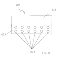
- FIG. 5 is an illustration of a cross-sectional view of another embodiment of a dielectric region for use within an energy conversion cell.
- the radius of the exciton orbit is also of importance.
- the probability of electron transfer to an interface (as for example in a solar cell embodiment) or to an atomic or molecular reactant (as in a photon energy conversion cell which utilizes chlorophyll) increases.
- the exciton orbit increases with increasing dielectric constant. Therefore not only are excitons drawn by the dielectric gradient towards the high dielectric region the transfer (or reaction) probability increase as it progresses.
- the relationship between dielectric constant and nominal Bohr exciton orbit radius, r B is:
Landscapes
- Chemical & Material Sciences (AREA)
- Chemical Kinetics & Catalysis (AREA)
- Electrochemistry (AREA)
- General Chemical & Material Sciences (AREA)
- Engineering & Computer Science (AREA)
- Power Engineering (AREA)
- Microelectronics & Electronic Packaging (AREA)
- Photovoltaic Devices (AREA)
- Hybrid Cells (AREA)
Priority Applications (1)
| Application Number | Priority Date | Filing Date | Title |
|---|---|---|---|
| US12/701,272 US8501332B2 (en) | 2009-02-05 | 2010-02-05 | Energy conversion cell having a dielectrically graded region to alter transport, and methods thereof |
Applications Claiming Priority (2)
| Application Number | Priority Date | Filing Date | Title |
|---|---|---|---|
| US15018209P | 2009-02-05 | 2009-02-05 | |
| US12/701,272 US8501332B2 (en) | 2009-02-05 | 2010-02-05 | Energy conversion cell having a dielectrically graded region to alter transport, and methods thereof |
Publications (2)
| Publication Number | Publication Date |
|---|---|
| US20100203364A1 US20100203364A1 (en) | 2010-08-12 |
| US8501332B2 true US8501332B2 (en) | 2013-08-06 |
Family
ID=42540666
Family Applications (1)
| Application Number | Title | Priority Date | Filing Date |
|---|---|---|---|
| US12/701,272 Expired - Fee Related US8501332B2 (en) | 2009-02-05 | 2010-02-05 | Energy conversion cell having a dielectrically graded region to alter transport, and methods thereof |
Country Status (10)
| Country | Link |
|---|---|
| US (1) | US8501332B2 (de) |
| EP (1) | EP2393750A2 (de) |
| JP (1) | JP2012517095A (de) |
| KR (1) | KR20110113636A (de) |
| CN (1) | CN102341876A (de) |
| AU (1) | AU2010210488A1 (de) |
| BR (1) | BRPI1008820A2 (de) |
| CA (1) | CA2751336A1 (de) |
| MX (1) | MX2011008042A (de) |
| WO (1) | WO2010091278A2 (de) |
Families Citing this family (5)
| Publication number | Priority date | Publication date | Assignee | Title |
|---|---|---|---|---|
| US9496426B2 (en) | 2012-02-10 | 2016-11-15 | Alliance For Sustainable Energy, Llc | Thin film photovoltaic devices with a minimally conductive buffer layer |
| WO2013173633A1 (en) * | 2012-05-16 | 2013-11-21 | Alliance For Sustainable Energy, Llc | Methods and materials for the improvement of photovoltaic device performance |
| US20150270423A1 (en) | 2012-11-19 | 2015-09-24 | Alliance For Sustainable Energy, Llc | Devices and methods featuring the addition of refractory metals to contact interface layers |
| AU2013352112A1 (en) * | 2012-11-28 | 2015-06-18 | The Regents Of The University Of Michigan | Hybrid planar-graded heterojunction for organic photovoltaics |
| FR3009892A1 (fr) * | 2013-08-20 | 2015-02-27 | Segton Adt | Ensemble opto-electronique forme d'une plateforme opto-phonique de traitement de la lumiere, de convertisseurs phoniques, et d'au moins un convertisseur lumiere-electricite pour former un capteur solaire |
Citations (7)
| Publication number | Priority date | Publication date | Assignee | Title |
|---|---|---|---|---|
| DE19647534A1 (de) | 1996-11-16 | 1998-05-28 | Dornier Gmbh | Elektrode für elektrochemische Energiewandler |
| EP1463073A1 (de) | 2003-03-24 | 2004-09-29 | Sony International (Europe) GmbH | Poröser Film mit einem Lichtstreuungsgradienten |
| US20050274411A1 (en) * | 2004-06-15 | 2005-12-15 | King Richard R | Solar cells having a transparent composition-graded buffer layer |
| JP2007123122A (ja) | 2005-10-28 | 2007-05-17 | Nissan Motor Co Ltd | 燃料電池用電解質膜および膜電極接合体 |
| US20080142075A1 (en) | 2006-12-06 | 2008-06-19 | Solexant Corporation | Nanophotovoltaic Device with Improved Quantum Efficiency |
| EP1936644A2 (de) | 2006-12-22 | 2008-06-25 | Sony Deutschland Gmbh | Photovoltaische Zelle |
| US8192789B2 (en) * | 2008-11-07 | 2012-06-05 | Sakti3, Inc. | Method for manufacture and structure of multiple electrochemistries and energy gathering components within a unified structure |
Family Cites Families (8)
| Publication number | Priority date | Publication date | Assignee | Title |
|---|---|---|---|---|
| JP5011610B2 (ja) * | 2001-05-28 | 2012-08-29 | 株式会社豊田中央研究所 | 無機材料複合高分子膜およびその製造方法 |
| KR20070015130A (ko) * | 2004-01-23 | 2007-02-01 | 더 유니버시티 오브 노쓰 캐롤라이나 엣 채플 힐 | 전기화학 전지에 사용하기 위한 액체 물질 |
| JP4710251B2 (ja) * | 2004-05-28 | 2011-06-29 | 凸版印刷株式会社 | 金属酸化物膜の製造方法 |
| JP5114823B2 (ja) * | 2004-05-31 | 2013-01-09 | 日産自動車株式会社 | 光電気化学電池 |
| JP2007157573A (ja) * | 2005-12-07 | 2007-06-21 | Toyota Motor Corp | 燃料電池 |
| JP2008177136A (ja) * | 2007-01-22 | 2008-07-31 | Nissan Motor Co Ltd | 燃料電池用触媒電極およびその製造方法 |
| JP5167680B2 (ja) * | 2007-04-17 | 2013-03-21 | アタカ大機株式会社 | Co汚染された固体高分子型可逆セルおよび燃料電池セルの水素極の性能を回復させる方法および装置 |
| US20090050201A1 (en) | 2007-07-17 | 2009-02-26 | The Research Foundation Of State University Of New York | Solar cell |
-
2010
- 2010-02-05 CN CN201080011413XA patent/CN102341876A/zh active Pending
- 2010-02-05 MX MX2011008042A patent/MX2011008042A/es active IP Right Grant
- 2010-02-05 JP JP2011549290A patent/JP2012517095A/ja active Pending
- 2010-02-05 EP EP10704458A patent/EP2393750A2/de not_active Withdrawn
- 2010-02-05 CA CA2751336A patent/CA2751336A1/en not_active Abandoned
- 2010-02-05 WO PCT/US2010/023358 patent/WO2010091278A2/en not_active Ceased
- 2010-02-05 AU AU2010210488A patent/AU2010210488A1/en not_active Abandoned
- 2010-02-05 US US12/701,272 patent/US8501332B2/en not_active Expired - Fee Related
- 2010-02-05 KR KR1020117019536A patent/KR20110113636A/ko not_active Ceased
- 2010-02-05 BR BRPI1008820A patent/BRPI1008820A2/pt not_active IP Right Cessation
Patent Citations (8)
| Publication number | Priority date | Publication date | Assignee | Title |
|---|---|---|---|---|
| DE19647534A1 (de) | 1996-11-16 | 1998-05-28 | Dornier Gmbh | Elektrode für elektrochemische Energiewandler |
| EP1463073A1 (de) | 2003-03-24 | 2004-09-29 | Sony International (Europe) GmbH | Poröser Film mit einem Lichtstreuungsgradienten |
| US20050274411A1 (en) * | 2004-06-15 | 2005-12-15 | King Richard R | Solar cells having a transparent composition-graded buffer layer |
| JP2007123122A (ja) | 2005-10-28 | 2007-05-17 | Nissan Motor Co Ltd | 燃料電池用電解質膜および膜電極接合体 |
| US20080142075A1 (en) | 2006-12-06 | 2008-06-19 | Solexant Corporation | Nanophotovoltaic Device with Improved Quantum Efficiency |
| TW200847449A (en) | 2006-12-06 | 2008-12-01 | Solexant Corp | Nanophotovoltaic device with improved quantum efficiency |
| EP1936644A2 (de) | 2006-12-22 | 2008-06-25 | Sony Deutschland Gmbh | Photovoltaische Zelle |
| US8192789B2 (en) * | 2008-11-07 | 2012-06-05 | Sakti3, Inc. | Method for manufacture and structure of multiple electrochemistries and energy gathering components within a unified structure |
Non-Patent Citations (1)
| Title |
|---|
| B. Pradhan et al., Organic photovoltaic devices: Concentration gradient of donor and acceptor materials in the molecular scale, 155 Synthetic Metals 555-559 (Dec. 15, 2005). |
Also Published As
| Publication number | Publication date |
|---|---|
| JP2012517095A (ja) | 2012-07-26 |
| AU2010210488A1 (en) | 2011-08-18 |
| CN102341876A (zh) | 2012-02-01 |
| WO2010091278A3 (en) | 2011-05-12 |
| CA2751336A1 (en) | 2010-08-12 |
| US20100203364A1 (en) | 2010-08-12 |
| EP2393750A2 (de) | 2011-12-14 |
| MX2011008042A (es) | 2012-07-03 |
| BRPI1008820A2 (pt) | 2016-03-01 |
| WO2010091278A2 (en) | 2010-08-12 |
| KR20110113636A (ko) | 2011-10-17 |
Similar Documents
| Publication | Publication Date | Title |
|---|---|---|
| Yue et al. | Electrostatic field enhanced photocatalytic CO2 conversion on BiVO4 nanowires | |
| Bisquert | Nanostructured energy devices: equilibrium concepts and kinetics | |
| Peng et al. | Silicon surface modification and characterization for emergent photovoltaic applications based on energy transfer | |
| Zhu et al. | Multiexciton annihilation and dissociation in quantum confined semiconductor nanocrystals | |
| Nozik et al. | Semiconductor quantum dots and quantum dot arrays and applications of multiple exciton generation to third-generation photovoltaic solar cells | |
| Hu et al. | Analysis of optical absorption in silicon nanowire arrays for photovoltaic applications | |
| Bisquert | The Physics of Solar Energy Conversion | |
| Zhang et al. | Effect of halide treatments on PbSe quantum dot thin films: Stability, hot carrier lifetime, and application to photovoltaics | |
| JP6381552B2 (ja) | 放射線分解電気化学的発電機 | |
| US8501332B2 (en) | Energy conversion cell having a dielectrically graded region to alter transport, and methods thereof | |
| Zhang et al. | TiO2 nanorods: a facile size-and shape-tunable synthesis and effective improvement of charge collection kinetics for dye-sensitized solar cells | |
| Mirnaziry et al. | Design and analysis of multi-layer silicon nanoparticle solar cells | |
| Sun et al. | Exploring the effect of band alignment and surface states on photoinduced electron transfer from CuInS2/CdS core/shell quantum dots to TiO2 electrodes | |
| US20090320914A1 (en) | Dye-sensitized solar cell and method of fabricating the same | |
| Miyake et al. | Characterization of covalently immobilized Q-CdS particles on Au (111) by scanning tunneling microscopy and tunneling spectroscopy with high reproducibility | |
| Song et al. | Enhancing the conversion efficiency of semiconductor sensitized solar cells via the cosensitization of dual-sized quantum dots | |
| Manousakis | Optimizing the role of impact ionization in conventional insulators | |
| Tu et al. | Photoinduced direct electron transfer from InSe to GaSe semiconductor nanoparticles | |
| Kennedy et al. | Primary Corrosion Processes for Polymer-Embedded Free-Standing or Substrate-Supported Silicon Microwire Arrays in Aqueous Alkaline Electrolytes | |
| Wei et al. | Electrochemical photovoltaic cells—review of recent developments | |
| McKone et al. | Structured materials for photoelectrochemical water splitting | |
| Javadi et al. | Ultra-low intensity UV detection using partitioned mesoporous TiO2 | |
| Lewerenz et al. | Concepts of Photoelectrochemical Energy Conversion and Fuel Generation | |
| Ahmmad et al. | TiO 2/TaON-and TiO 2/BiOI-based solid-state solar cells | |
| Toyoda et al. | Crystal Growth, Exponential Optical Absorption Edge, and Ground State Energy Level of PbS Quantum Dots Adsorbed on the (001),(110), and (111) Surfaces of Rutile-TiO2 |
Legal Events
| Date | Code | Title | Description |
|---|---|---|---|
| AS | Assignment |
Owner name: THE RESEARCH FOUNDATION OF STATE UNIVERSITY OF NEW Free format text: ASSIGNMENT OF ASSIGNORS INTEREST;ASSIGNOR:FORTMANN, CHARLES M.;REEL/FRAME:024299/0631 Effective date: 20100330 |
|
| STCF | Information on status: patent grant |
Free format text: PATENTED CASE |
|
| FPAY | Fee payment |
Year of fee payment: 4 |
|
| FEPP | Fee payment procedure |
Free format text: MAINTENANCE FEE REMINDER MAILED (ORIGINAL EVENT CODE: REM.); ENTITY STATUS OF PATENT OWNER: SMALL ENTITY |
|
| LAPS | Lapse for failure to pay maintenance fees |
Free format text: PATENT EXPIRED FOR FAILURE TO PAY MAINTENANCE FEES (ORIGINAL EVENT CODE: EXP.); ENTITY STATUS OF PATENT OWNER: SMALL ENTITY |
|
| STCH | Information on status: patent discontinuation |
Free format text: PATENT EXPIRED DUE TO NONPAYMENT OF MAINTENANCE FEES UNDER 37 CFR 1.362 |
|
| FP | Lapsed due to failure to pay maintenance fee |
Effective date: 20210806 |