US8377848B2 - Donor substrate and method of manufacturing display - Google Patents
Donor substrate and method of manufacturing display Download PDFInfo
- Publication number
- US8377848B2 US8377848B2 US13/100,612 US201113100612A US8377848B2 US 8377848 B2 US8377848 B2 US 8377848B2 US 201113100612 A US201113100612 A US 201113100612A US 8377848 B2 US8377848 B2 US 8377848B2
- Authority
- US
- United States
- Prior art keywords
- layer
- light emitting
- electrode
- substrate
- heat insulating
- Prior art date
- Legal status (The legal status is an assumption and is not a legal conclusion. Google has not performed a legal analysis and makes no representation as to the accuracy of the status listed.)
- Expired - Fee Related
Links
- 239000000758 substrate Substances 0.000 title claims abstract description 194
- 238000004519 manufacturing process Methods 0.000 title claims description 27
- 238000012546 transfer Methods 0.000 claims abstract description 97
- 238000006243 chemical reaction Methods 0.000 claims abstract description 56
- 239000000463 material Substances 0.000 claims abstract description 38
- 238000000034 method Methods 0.000 claims abstract description 26
- 230000001678 irradiating effect Effects 0.000 claims abstract description 10
- 230000008016 vaporization Effects 0.000 claims abstract description 8
- 239000010410 layer Substances 0.000 claims description 488
- VYPSYNLAJGMNEJ-UHFFFAOYSA-N Silicium dioxide Chemical compound O=[Si]=O VYPSYNLAJGMNEJ-UHFFFAOYSA-N 0.000 claims description 25
- 239000012044 organic layer Substances 0.000 claims description 24
- 229910052681 coesite Inorganic materials 0.000 claims description 12
- 229910052906 cristobalite Inorganic materials 0.000 claims description 12
- 239000000377 silicon dioxide Substances 0.000 claims description 12
- 229910052682 stishovite Inorganic materials 0.000 claims description 12
- 229910052905 tridymite Inorganic materials 0.000 claims description 12
- 229910021417 amorphous silicon Inorganic materials 0.000 claims description 11
- 239000003086 colorant Substances 0.000 claims description 5
- 229910052814 silicon oxide Inorganic materials 0.000 claims description 4
- 229910004541 SiN Inorganic materials 0.000 claims description 3
- PNEYBMLMFCGWSK-UHFFFAOYSA-N aluminium oxide Inorganic materials [O-2].[O-2].[O-2].[Al+3].[Al+3] PNEYBMLMFCGWSK-UHFFFAOYSA-N 0.000 claims description 3
- 229910052593 corundum Inorganic materials 0.000 claims description 3
- 229910001845 yogo sapphire Inorganic materials 0.000 claims description 3
- 238000000859 sublimation Methods 0.000 claims 2
- 230000008022 sublimation Effects 0.000 claims 2
- 238000009834 vaporization Methods 0.000 claims 2
- 230000002452 interceptive effect Effects 0.000 abstract description 80
- 230000005855 radiation Effects 0.000 abstract description 34
- 239000010408 film Substances 0.000 description 29
- 230000002829 reductive effect Effects 0.000 description 20
- 230000001681 protective effect Effects 0.000 description 18
- 230000000052 comparative effect Effects 0.000 description 15
- 230000004048 modification Effects 0.000 description 14
- 238000012986 modification Methods 0.000 description 14
- 239000011521 glass Substances 0.000 description 11
- 238000007789 sealing Methods 0.000 description 11
- 238000010521 absorption reaction Methods 0.000 description 10
- 238000000151 deposition Methods 0.000 description 10
- 238000009792 diffusion process Methods 0.000 description 10
- 238000001704 evaporation Methods 0.000 description 10
- 229910052751 metal Inorganic materials 0.000 description 9
- 239000002184 metal Substances 0.000 description 9
- 238000000862 absorption spectrum Methods 0.000 description 8
- 239000000956 alloy Substances 0.000 description 8
- 229910045601 alloy Inorganic materials 0.000 description 8
- 239000010936 titanium Substances 0.000 description 8
- 229910052736 halogen Inorganic materials 0.000 description 7
- 150000002367 halogens Chemical class 0.000 description 7
- 229910052724 xenon Inorganic materials 0.000 description 7
- FHNFHKCVQCLJFQ-UHFFFAOYSA-N xenon atom Chemical compound [Xe] FHNFHKCVQCLJFQ-UHFFFAOYSA-N 0.000 description 7
- 229910052782 aluminium Inorganic materials 0.000 description 6
- XAGFODPZIPBFFR-UHFFFAOYSA-N aluminium Chemical compound [Al] XAGFODPZIPBFFR-UHFFFAOYSA-N 0.000 description 6
- 239000000203 mixture Substances 0.000 description 6
- 238000002834 transmittance Methods 0.000 description 6
- VYZAMTAEIAYCRO-UHFFFAOYSA-N Chromium Chemical compound [Cr] VYZAMTAEIAYCRO-UHFFFAOYSA-N 0.000 description 5
- 230000008021 deposition Effects 0.000 description 5
- 239000011159 matrix material Substances 0.000 description 5
- 238000000206 photolithography Methods 0.000 description 5
- 239000011347 resin Substances 0.000 description 5
- 229920005989 resin Polymers 0.000 description 5
- TVIVIEFSHFOWTE-UHFFFAOYSA-K tri(quinolin-8-yloxy)alumane Chemical compound [Al+3].C1=CN=C2C([O-])=CC=CC2=C1.C1=CN=C2C([O-])=CC=CC2=C1.C1=CN=C2C([O-])=CC=CC2=C1 TVIVIEFSHFOWTE-UHFFFAOYSA-K 0.000 description 5
- DIVZFUBWFAOMCW-UHFFFAOYSA-N 4-n-(3-methylphenyl)-1-n,1-n-bis[4-(n-(3-methylphenyl)anilino)phenyl]-4-n-phenylbenzene-1,4-diamine Chemical compound CC1=CC=CC(N(C=2C=CC=CC=2)C=2C=CC(=CC=2)N(C=2C=CC(=CC=2)N(C=2C=CC=CC=2)C=2C=C(C)C=CC=2)C=2C=CC(=CC=2)N(C=2C=CC=CC=2)C=2C=C(C)C=CC=2)=C1 DIVZFUBWFAOMCW-UHFFFAOYSA-N 0.000 description 4
- ZOKXTWBITQBERF-UHFFFAOYSA-N Molybdenum Chemical compound [Mo] ZOKXTWBITQBERF-UHFFFAOYSA-N 0.000 description 4
- RTAQQCXQSZGOHL-UHFFFAOYSA-N Titanium Chemical compound [Ti] RTAQQCXQSZGOHL-UHFFFAOYSA-N 0.000 description 4
- 238000005229 chemical vapour deposition Methods 0.000 description 4
- 229910052750 molybdenum Inorganic materials 0.000 description 4
- 239000011733 molybdenum Substances 0.000 description 4
- IBHBKWKFFTZAHE-UHFFFAOYSA-N n-[4-[4-(n-naphthalen-1-ylanilino)phenyl]phenyl]-n-phenylnaphthalen-1-amine Chemical compound C1=CC=CC=C1N(C=1C2=CC=CC=C2C=CC=1)C1=CC=C(C=2C=CC(=CC=2)N(C=2C=CC=CC=2)C=2C3=CC=CC=C3C=CC=2)C=C1 IBHBKWKFFTZAHE-UHFFFAOYSA-N 0.000 description 4
- 239000011368 organic material Substances 0.000 description 4
- 229920001721 polyimide Polymers 0.000 description 4
- 238000009751 slip forming Methods 0.000 description 4
- 238000004544 sputter deposition Methods 0.000 description 4
- 229910052719 titanium Inorganic materials 0.000 description 4
- PXHVJJICTQNCMI-UHFFFAOYSA-N Nickel Chemical compound [Ni] PXHVJJICTQNCMI-UHFFFAOYSA-N 0.000 description 3
- 239000004642 Polyimide Substances 0.000 description 3
- ATJFFYVFTNAWJD-UHFFFAOYSA-N Tin Chemical compound [Sn] ATJFFYVFTNAWJD-UHFFFAOYSA-N 0.000 description 3
- 230000006866 deterioration Effects 0.000 description 3
- QDOXWKRWXJOMAK-UHFFFAOYSA-N dichromium trioxide Chemical compound O=[Cr]O[Cr]=O QDOXWKRWXJOMAK-UHFFFAOYSA-N 0.000 description 3
- 239000011777 magnesium Substances 0.000 description 3
- 230000014759 maintenance of location Effects 0.000 description 3
- 238000002156 mixing Methods 0.000 description 3
- 230000003287 optical effect Effects 0.000 description 3
- BASFCYQUMIYNBI-UHFFFAOYSA-N platinum Chemical compound [Pt] BASFCYQUMIYNBI-UHFFFAOYSA-N 0.000 description 3
- 230000008569 process Effects 0.000 description 3
- 230000009467 reduction Effects 0.000 description 3
- 239000002356 single layer Substances 0.000 description 3
- 239000010409 thin film Substances 0.000 description 3
- XLYOFNOQVPJJNP-UHFFFAOYSA-N water Substances O XLYOFNOQVPJJNP-UHFFFAOYSA-N 0.000 description 3
- FYYHWMGAXLPEAU-UHFFFAOYSA-N Magnesium Chemical compound [Mg] FYYHWMGAXLPEAU-UHFFFAOYSA-N 0.000 description 2
- BQCADISMDOOEFD-UHFFFAOYSA-N Silver Chemical compound [Ag] BQCADISMDOOEFD-UHFFFAOYSA-N 0.000 description 2
- 230000008901 benefit Effects 0.000 description 2
- 230000015572 biosynthetic process Effects 0.000 description 2
- 239000011575 calcium Substances 0.000 description 2
- 239000003990 capacitor Substances 0.000 description 2
- 239000002131 composite material Substances 0.000 description 2
- 239000010949 copper Substances 0.000 description 2
- 230000000694 effects Effects 0.000 description 2
- 239000010931 gold Substances 0.000 description 2
- 238000003384 imaging method Methods 0.000 description 2
- 239000011810 insulating material Substances 0.000 description 2
- 229910052749 magnesium Inorganic materials 0.000 description 2
- 238000000059 patterning Methods 0.000 description 2
- 230000035699 permeability Effects 0.000 description 2
- 238000012545 processing Methods 0.000 description 2
- 238000005215 recombination Methods 0.000 description 2
- 230000006798 recombination Effects 0.000 description 2
- 230000000717 retained effect Effects 0.000 description 2
- HQVNEWCFYHHQES-UHFFFAOYSA-N silicon nitride Chemical compound N12[Si]34N5[Si]62N3[Si]51N64 HQVNEWCFYHHQES-UHFFFAOYSA-N 0.000 description 2
- 229910052709 silver Inorganic materials 0.000 description 2
- 239000004332 silver Substances 0.000 description 2
- 239000000126 substance Substances 0.000 description 2
- 238000001771 vacuum deposition Methods 0.000 description 2
- XSUNFLLNZQIJJG-UHFFFAOYSA-N 2-n-naphthalen-2-yl-1-n,1-n,2-n-triphenylbenzene-1,2-diamine Chemical compound C1=CC=CC=C1N(C=1C(=CC=CC=1)N(C=1C=CC=CC=1)C=1C=C2C=CC=CC2=CC=1)C1=CC=CC=C1 XSUNFLLNZQIJJG-UHFFFAOYSA-N 0.000 description 1
- OSQXTXTYKAEHQV-WXUKJITCSA-N 4-methyl-n-[4-[(e)-2-[4-[4-[(e)-2-[4-(4-methyl-n-(4-methylphenyl)anilino)phenyl]ethenyl]phenyl]phenyl]ethenyl]phenyl]-n-(4-methylphenyl)aniline Chemical compound C1=CC(C)=CC=C1N(C=1C=CC(\C=C\C=2C=CC(=CC=2)C=2C=CC(\C=C\C=3C=CC(=CC=3)N(C=3C=CC(C)=CC=3)C=3C=CC(C)=CC=3)=CC=2)=CC=1)C1=CC=C(C)C=C1 OSQXTXTYKAEHQV-WXUKJITCSA-N 0.000 description 1
- VIZUPBYFLORCRA-UHFFFAOYSA-N 9,10-dinaphthalen-2-ylanthracene Chemical compound C12=CC=CC=C2C(C2=CC3=CC=CC=C3C=C2)=C(C=CC=C2)C2=C1C1=CC=C(C=CC=C2)C2=C1 VIZUPBYFLORCRA-UHFFFAOYSA-N 0.000 description 1
- 229920000178 Acrylic resin Polymers 0.000 description 1
- 239000004925 Acrylic resin Substances 0.000 description 1
- 229910017073 AlLi Inorganic materials 0.000 description 1
- OYPRJOBELJOOCE-UHFFFAOYSA-N Calcium Chemical compound [Ca] OYPRJOBELJOOCE-UHFFFAOYSA-N 0.000 description 1
- 206010061781 Complication of delivery Diseases 0.000 description 1
- RYGMFSIKBFXOCR-UHFFFAOYSA-N Copper Chemical compound [Cu] RYGMFSIKBFXOCR-UHFFFAOYSA-N 0.000 description 1
- FUJCRWPEOMXPAD-UHFFFAOYSA-N Li2O Inorganic materials [Li+].[Li+].[O-2] FUJCRWPEOMXPAD-UHFFFAOYSA-N 0.000 description 1
- WHXSMMKQMYFTQS-UHFFFAOYSA-N Lithium Chemical compound [Li] WHXSMMKQMYFTQS-UHFFFAOYSA-N 0.000 description 1
- 229910052581 Si3N4 Inorganic materials 0.000 description 1
- 229910004205 SiNX Inorganic materials 0.000 description 1
- KEAYESYHFKHZAL-UHFFFAOYSA-N Sodium Chemical compound [Na] KEAYESYHFKHZAL-UHFFFAOYSA-N 0.000 description 1
- 239000007983 Tris buffer Substances 0.000 description 1
- 229910021431 alpha silicon carbide Inorganic materials 0.000 description 1
- 230000004075 alteration Effects 0.000 description 1
- 229910003481 amorphous carbon Inorganic materials 0.000 description 1
- QVGXLLKOCUKJST-UHFFFAOYSA-N atomic oxygen Chemical compound [O] QVGXLLKOCUKJST-UHFFFAOYSA-N 0.000 description 1
- HFACYLZERDEVSX-UHFFFAOYSA-N benzidine Chemical compound C1=CC(N)=CC=C1C1=CC=C(N)C=C1 HFACYLZERDEVSX-UHFFFAOYSA-N 0.000 description 1
- 239000000872 buffer Substances 0.000 description 1
- 229910052791 calcium Inorganic materials 0.000 description 1
- 238000004364 calculation method Methods 0.000 description 1
- 230000001413 cellular effect Effects 0.000 description 1
- 230000008859 change Effects 0.000 description 1
- 239000004020 conductor Substances 0.000 description 1
- 229910052802 copper Inorganic materials 0.000 description 1
- VBVAVBCYMYWNOU-UHFFFAOYSA-N coumarin 6 Chemical compound C1=CC=C2SC(C3=CC4=CC=C(C=C4OC3=O)N(CC)CC)=NC2=C1 VBVAVBCYMYWNOU-UHFFFAOYSA-N 0.000 description 1
- 238000013461 design Methods 0.000 description 1
- 238000011161 development Methods 0.000 description 1
- XUCJHNOBJLKZNU-UHFFFAOYSA-M dilithium;hydroxide Chemical compound [Li+].[Li+].[OH-] XUCJHNOBJLKZNU-UHFFFAOYSA-M 0.000 description 1
- 238000001312 dry etching Methods 0.000 description 1
- 238000001035 drying Methods 0.000 description 1
- 230000005684 electric field Effects 0.000 description 1
- 238000005401 electroluminescence Methods 0.000 description 1
- 238000000295 emission spectrum Methods 0.000 description 1
- 238000005530 etching Methods 0.000 description 1
- 230000008020 evaporation Effects 0.000 description 1
- PCHJSUWPFVWCPO-UHFFFAOYSA-N gold Chemical compound [Au] PCHJSUWPFVWCPO-UHFFFAOYSA-N 0.000 description 1
- 229910052737 gold Inorganic materials 0.000 description 1
- 238000010438 heat treatment Methods 0.000 description 1
- 229910052738 indium Inorganic materials 0.000 description 1
- APFVFJFRJDLVQX-UHFFFAOYSA-N indium atom Chemical compound [In] APFVFJFRJDLVQX-UHFFFAOYSA-N 0.000 description 1
- RHZWSUVWRRXEJF-UHFFFAOYSA-N indium tin Chemical compound [In].[Sn] RHZWSUVWRRXEJF-UHFFFAOYSA-N 0.000 description 1
- NJWNEWQMQCGRDO-UHFFFAOYSA-N indium zinc Chemical compound [Zn].[In] NJWNEWQMQCGRDO-UHFFFAOYSA-N 0.000 description 1
- AMGQUBHHOARCQH-UHFFFAOYSA-N indium;oxotin Chemical compound [In].[Sn]=O AMGQUBHHOARCQH-UHFFFAOYSA-N 0.000 description 1
- 238000002347 injection Methods 0.000 description 1
- 239000007924 injection Substances 0.000 description 1
- 229910052743 krypton Inorganic materials 0.000 description 1
- DNNSSWSSYDEUBZ-UHFFFAOYSA-N krypton atom Chemical compound [Kr] DNNSSWSSYDEUBZ-UHFFFAOYSA-N 0.000 description 1
- 239000007788 liquid Substances 0.000 description 1
- 229910052744 lithium Inorganic materials 0.000 description 1
- 238000001459 lithography Methods 0.000 description 1
- 239000007769 metal material Substances 0.000 description 1
- YPJRZWDWVBNDIW-MBALSZOMSA-N n,n-diphenyl-4-[(e)-2-[4-[4-[(e)-2-[4-(n-phenylanilino)phenyl]ethenyl]phenyl]phenyl]ethenyl]aniline Chemical group C=1C=C(N(C=2C=CC=CC=2)C=2C=CC=CC=2)C=CC=1/C=C/C(C=C1)=CC=C1C(C=C1)=CC=C1\C=C\C(C=C1)=CC=C1N(C=1C=CC=CC=1)C1=CC=CC=C1 YPJRZWDWVBNDIW-MBALSZOMSA-N 0.000 description 1
- 229910052759 nickel Inorganic materials 0.000 description 1
- AHLBNYSZXLDEJQ-FWEHEUNISA-N orlistat Chemical compound CCCCCCCCCCC[C@H](OC(=O)[C@H](CC(C)C)NC=O)C[C@@H]1OC(=O)[C@H]1CCCCCC AHLBNYSZXLDEJQ-FWEHEUNISA-N 0.000 description 1
- 229910052760 oxygen Inorganic materials 0.000 description 1
- 239000001301 oxygen Substances 0.000 description 1
- 239000002245 particle Substances 0.000 description 1
- 229910052697 platinum Inorganic materials 0.000 description 1
- 239000009719 polyimide resin Substances 0.000 description 1
- 239000011241 protective layer Substances 0.000 description 1
- 230000004043 responsiveness Effects 0.000 description 1
- 230000002441 reversible effect Effects 0.000 description 1
- HBMJWWWQQXIZIP-UHFFFAOYSA-N silicon carbide Chemical compound [Si+]#[C-] HBMJWWWQQXIZIP-UHFFFAOYSA-N 0.000 description 1
- 125000005504 styryl group Chemical group 0.000 description 1
- WFKWXMTUELFFGS-UHFFFAOYSA-N tungsten Chemical compound [W] WFKWXMTUELFFGS-UHFFFAOYSA-N 0.000 description 1
- 229910052721 tungsten Inorganic materials 0.000 description 1
- 239000010937 tungsten Substances 0.000 description 1
- 230000000007 visual effect Effects 0.000 description 1
Images


Classifications
-
- C—CHEMISTRY; METALLURGY
- C23—COATING METALLIC MATERIAL; COATING MATERIAL WITH METALLIC MATERIAL; CHEMICAL SURFACE TREATMENT; DIFFUSION TREATMENT OF METALLIC MATERIAL; COATING BY VACUUM EVAPORATION, BY SPUTTERING, BY ION IMPLANTATION OR BY CHEMICAL VAPOUR DEPOSITION, IN GENERAL; INHIBITING CORROSION OF METALLIC MATERIAL OR INCRUSTATION IN GENERAL
- C23C—COATING METALLIC MATERIAL; COATING MATERIAL WITH METALLIC MATERIAL; SURFACE TREATMENT OF METALLIC MATERIAL BY DIFFUSION INTO THE SURFACE, BY CHEMICAL CONVERSION OR SUBSTITUTION; COATING BY VACUUM EVAPORATION, BY SPUTTERING, BY ION IMPLANTATION OR BY CHEMICAL VAPOUR DEPOSITION, IN GENERAL
- C23C14/00—Coating by vacuum evaporation, by sputtering or by ion implantation of the coating forming material
- C23C14/04—Coating on selected surface areas, e.g. using masks
- C23C14/048—Coating on selected surface areas, e.g. using masks using irradiation by energy or particles
-
- H—ELECTRICITY
- H10—SEMICONDUCTOR DEVICES; ELECTRIC SOLID-STATE DEVICES NOT OTHERWISE PROVIDED FOR
- H10K—ORGANIC ELECTRIC SOLID-STATE DEVICES
- H10K71/00—Manufacture or treatment specially adapted for the organic devices covered by this subclass
- H10K71/10—Deposition of organic active material
- H10K71/18—Deposition of organic active material using non-liquid printing techniques, e.g. thermal transfer printing from a donor sheet
-
- H—ELECTRICITY
- H10—SEMICONDUCTOR DEVICES; ELECTRIC SOLID-STATE DEVICES NOT OTHERWISE PROVIDED FOR
- H10K—ORGANIC ELECTRIC SOLID-STATE DEVICES
- H10K59/00—Integrated devices, or assemblies of multiple devices, comprising at least one organic light-emitting element covered by group H10K50/00
- H10K59/30—Devices specially adapted for multicolour light emission
- H10K59/35—Devices specially adapted for multicolour light emission comprising red-green-blue [RGB] subpixels
-
- H—ELECTRICITY
- H10—SEMICONDUCTOR DEVICES; ELECTRIC SOLID-STATE DEVICES NOT OTHERWISE PROVIDED FOR
- H10K—ORGANIC ELECTRIC SOLID-STATE DEVICES
- H10K71/00—Manufacture or treatment specially adapted for the organic devices covered by this subclass
-
- H—ELECTRICITY
- H10—SEMICONDUCTOR DEVICES; ELECTRIC SOLID-STATE DEVICES NOT OTHERWISE PROVIDED FOR
- H10K—ORGANIC ELECTRIC SOLID-STATE DEVICES
- H10K71/00—Manufacture or treatment specially adapted for the organic devices covered by this subclass
- H10K71/40—Thermal treatment, e.g. annealing in the presence of a solvent vapour
- H10K71/421—Thermal treatment, e.g. annealing in the presence of a solvent vapour using coherent electromagnetic radiation, e.g. laser annealing
-
- Y—GENERAL TAGGING OF NEW TECHNOLOGICAL DEVELOPMENTS; GENERAL TAGGING OF CROSS-SECTIONAL TECHNOLOGIES SPANNING OVER SEVERAL SECTIONS OF THE IPC; TECHNICAL SUBJECTS COVERED BY FORMER USPC CROSS-REFERENCE ART COLLECTIONS [XRACs] AND DIGESTS
- Y10—TECHNICAL SUBJECTS COVERED BY FORMER USPC
- Y10S—TECHNICAL SUBJECTS COVERED BY FORMER USPC CROSS-REFERENCE ART COLLECTIONS [XRACs] AND DIGESTS
- Y10S430/00—Radiation imagery chemistry: process, composition, or product thereof
- Y10S430/146—Laser beam
Definitions
- the present invention relates to a donor substrate used in forming a light emitting layer in an organic light emitting device by transfer method, and a method of manufacturing a display using such a donor substrate.
- organic light emitting display using an organic light emitting device (organic EL (electroluminescence) device) in which a first electrode, a plurality of organic layers including a light emitting layer, and a second electrode are stacked in this order on a driving substrate has attracted attention. Since the organic light emitting display is self-emitting, it has a large view angle. In the organic light emitting display, since a backlight is unnecessary, electric power saving is expected. Moreover, responsiveness is high, and low-profile of the display is possible. Therefore, it is highly desired that the organic light emitting display be applied to a large-screen display such as a television.
- organic EL organic EL
- a transfer method in which a radiation ray such as a laser is used.
- a donor element provided with a transfer layer containing light emission material as supporting material is formed, and the donor element faces a substrate to be transferred for forming the organic light emitting device.
- the transfer layer is transferred to the substrate to be transferred by irradiating a radiation ray under a reduced-pressure environment.
- the radiation ray there is a case where light from a xenon flash lamp is condensed by a lens and used (for example, refer to Japanese Unexamined Patent Publication No. 1997-167684 (paragraphs 0017 and 0028)).
- a photothermal conversion layer of chrome (Cr) or the like is patterned to only a desired region (region desired to be transferred) in a base of glass or a film.
- a transfer step a transfer layer of organic material is formed on a donor substrate, and laser light is locally irradiated corresponding to the photothermal conversion layer. Thereby, only the desired range in the transfer layer is transferred to a substrate to be transferred.
- a xenon flash lamp, a halogen infrared lamp, and the like are considered promising as radiation sources replacing the laser, since a collective or traversable processing may be performed in a large area.
- a donor substrate capable of efficiently absorbing a radiation ray with a wide wavelength such as a flash lamp and a halogen infrared lamp has not been developed in the related art, and large power loss occurs in the case of using a donor substrate of the related art.
- a surface of the base and the photothermal conversion layer are covered with a heat insulating layer of SiO 2 or the like, and a pollution preventing layer of molybdenum (Mo) or the like is formed on the heat insulating layer.
- a pollution preventing layer of molybdenum (Mo) or the like is formed on the heat insulating layer.
- a donor substrate capable of efficiently absorbing a radiation ray with a wide wavelength and a method of manufacturing a display using the donor substrate.
- a first donor substrate used in forming a light emitting layer by forming a transfer layer containing light emission material, irradiating a radiation ray to the transfer layer while the transfer layer and a substrate to be transferred face each other, and sublimating or vaporizing the transfer layer so that the transfer layer is transferred to the substrate to be transferred.
- the donor substrate includes the following components (A) to (C).
- a second donor substrate used in forming a light emitting layer by forming a transfer layer containing light emission material, irradiating a radiation ray while the transfer layer and a substrate to be transferred face each other, and sublimating or vaporizing the transfer layer so that the transfer layer is transferred to the substrate to be transferred.
- the donor substrate includes the following components (A) to (E).
- a first method or a second method of manufacturing a display according to embodiments of the present invention in which an organic light emitting device including a first electrode, an insulating layer including an aperture corresponding to a light emitting region of the first electrode, a plurality of organic layers including a light emitting layer, and a second electrode in this order is formed on a driving substrate includes the steps of: forming the first electrode, the insulating layer, a part of the plurality of organic layers on the driving substrate, thereby forming a substrate to be transferred; forming a transfer layer containing light emission material in a donor substrate, irradiating a radiation ray while the transfer layer and the substrate to be transferred face each other, and sublimating or vaporizing the transfer layer so that the transfer layer is transferred to the substrate to be transferred, thereby forming a light emitting layer; and forming remains of the plurality of organic layers and the second electrode.
- the donor substrate the first or the second donor substrate according to the embodiments of the present invention is used.
- a heat interfering layer including two or more layers with refraction index different from each other is arranged between the base and the photothermal conversion layer.
- the pollution preventing layer includes a first portion formed on a top surface of the convex structure and a second portion formed on a top surface of the heat insulating layer, and the first portion and the second portion are separated from each other.
- heat diffusion through the pollution preventing layer is highly reduced.
- a risk that an undesired range in the transfer layer is transferred is reduced, and a desired range is transferred with high accuracy.
- a heat interfering layer including two or more layers with refraction index different from each other is arranged between the base and the photothermal conversion layer.
- the absorption improves in a wide wavelength range by adjusting refraction index (material) and the thickness of the heat interfering layer.
- the pollution preventing layer includes a first portion formed on a top surface of the convex structure and a second portion formed on a top surface of the heat insulating layer, and the first portion and the second portion are separated from each other.
- the heat diffusion through the pollution preventing layer is highly reduced, and the desired range in the transfer layer is transferred with high accuracy. Therefore, when manufacturing the organic light emitting display by using the donor substrate, the light emitting layer is formed with high precision without using a mask.
- FIG. 1 is a view illustrating the configuration of a display according to a first embodiment of the present invention.
- FIG. 2 is a view illustrating an example of a pixel driving circuit in FIG. 1 .
- FIG. 3 is a cross-sectional view illustrating the configuration of a display region in FIG. 1 .
- FIGS. 4A to 4C are plan views illustrating the configuration of a first electrode and an insulating layer in FIG. 3 .
- FIG. 5 is a cross-sectional plan view illustrating the configuration of a donor substrate used in a method of manufacturing the display in FIG. 1 .
- FIGS. 6A and 6B are cross sectional views illustrating a method of manufacturing the donor substrate in process order.
- FIGS. 7A and 7B are cross sectional views illustrating a method of manufacturing the display in FIG. 1 in process order.
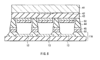
- FIG. 8 is a cross-sectional view for explaining operation of a rib in FIGS. 4A to 4C .
- FIGS. 9A and 9B are cross-sectional views for explaining an example and an issue of a donor substrate of the related art.
- FIG. 10 is a cross-sectional view illustrating a modification of the step in FIG. 7B .
- FIG. 11 is a cross-sectional view illustrating a modification of the donor substrate in FIG. 5 .
- FIG. 12 is a cross-sectional view illustrating the method of manufacturing the display using the donor substrate in FIG. 11 .
- FIG. 13 is a cross-sectional view illustrating a modification of the step in FIG. 12 .
- FIG. 14 is a cross-sectional view illustrating the configuration of a donor substrate according to a second embodiment of the present invention.
- FIG. 15 is a cross-sectional view illustrating a donor substrate according to a third embodiment of the present invention.
- FIG. 16 is a view illustrating an absorption spectrum in a heat interfering layer.
- FIG. 17 is a view illustrating the absorption spectrum in the heat interfering layer.
- FIG. 18 is a view illustrating the absorption spectrum in the heat interfering layer.
- FIG. 19 is a cross-sectional view illustrating a transfer step by using the donor substrate in FIG. 15 .
- FIG. 20 is a plan view illustrating an example of a method of irradiating a radiation ray.
- FIG. 21 is a plan view illustrating another example of the method of irradiating the radiation ray.
- FIG. 22 is a cross-sectional view illustrating a modification of the donor substrate in FIG. 15 .
- FIGS. 23A and 23B are cross-sectional views for explaining the configuration and an issue of a donor substrate in Comparative example 1.
- FIG. 24 is a plan view illustrating the schematic configuration of a module including the display in the first to third embodiments.
- FIG. 25 is a perspective view illustrating appearance of Application example 1 of the display in the first to third embodiments.
- FIG. 26A is a perspective view illustrating appearance as seen from a front side of Application example 2
- FIG. 26B is a perspective view illustrating appearance as seen from a rear side of Application example 2.
- FIG. 27 is a perspective view illustrating appearance of Application example 3.
- FIG. 28 is a perspective view illustrating appearance of Application example 4.
- FIG. 29A is a front view in an opened state of Application example 5
- FIG. 29B is a side view in the opened state
- FIG. 29C is a front view in a closed state
- FIG. 29D is a left side view in the closed state
- FIG. 29E is a right side view in the closed state
- FIG. 29F is a top view in the closed state
- FIG. 29G is a bottom view in the closed state.
- FIG. 30 is a cross-sectional view illustrating the configuration of a display region after formation of a blue-light emitting layer.
- First embodiment (example where laser light is used as a radiation ray and a convex structure is provided in a donor substrate).
- Second embodiment (example where a heat interfering layer with a single-layer structure is provided between a base and a photothermal conversion layer).
- FIG. 1 illustrates the configuration of a display according to a first embodiment of the present invention.
- the display is used as a low-profile organic light emitting color display or the like.
- a display region 110 in which a plurality of light emitting devices 10 R, 10 G, and 10 B which will be described later are arranged in matrix is formed on a driving substrate 11 of glass, and a signal line driving circuit 120 and a scanning line driving circuit 130 as drivers for image display are formed in vicinity of the display region 110 .
- FIG. 2 illustrates an example of the pixel driving circuit 140 .
- the pixel driving circuit 140 is formed in a layer level below that of a first electrode 13 which will be described later.
- the pixel driving circuit 140 is an active driving circuit including a driving transistor Tr 1 and a writing transistor Tr 2 , a capacitor Cs (retention capacity) arranged between the driving transistor Tr 1 and the writing transistor Tr 2 , and the organic light emitting device 10 R (or 10 G or 10 B) connected in series to the driving transistor Tr 1 between a first power source line (Vcc) and a second power source line (GND).
- the driving transistor Tr 1 and the writing transistor Tr 2 are configured with a typical thin film transistor (TFT).
- TFT thin film transistor
- the structure of the TFT is not specifically limited, and may be an inverted staggered structure (so-called bottom-gate type) or a staggered structure (top-gate type).
- a plurality of signal lines 120 A are arranged in a column direction, and a plurality of scanning lines 130 A are arranged in a row direction.
- An intersection between each signal line 120 A and each scanning line 130 A corresponds to either one (sub-pixel) of the organic light emitting devices 10 R, 10 G and 10 B.
- Each signal line 120 A is connected to the signal line driving circuit 120 , and an image signal is supplied from the signal line driving circuit 120 to a source electrode of the writing transistor Tr 2 through the signal line 120 A.
- Each scanning line 130 A is connected to the scanning line driving circuit 130 , and a scanning signal is supplied in sequence from the scanning line driving circuit 130 to a gate electrode of the writing transistor Tr 2 through the scanning line 130 A.
- FIG. 3 illustrates an example of the cross-sectional configuration of the display region 110 .
- the organic light emitting device 10 R generating red light
- the organic light emitting device 10 G generating green light
- the organic light emitting device 10 B generating blue light are formed in this order in matrix as a whole.
- the organic light emitting devices 10 R, 10 G, and 10 B have a rectangular flat shape, and are arranged in a longitudinal direction (column direction) for each color.
- a combination of the organic light emitting devices 10 R, 10 G, and 10 B immediately adjacent to one another constitute one pixel.
- Pixel pitch is, for example, 300 ⁇ m.
- a first electrode 13 as an anode, an insulating layer 14 , an organic layer 15 including a red light emitting layer 15 CR, a green light emitting layer 15 CG, or a blue light emitting layer 15 CB which will be described later, and a second electrode 16 as a cathode are stacked in this order from the driving substrate 11 side with a driving transistor (not illustrated in the figure) and a planarized insulating film (not illustrated in the figure) in the above-described pixel driving circuit 140 in between.
- Such organic light emitting devices 10 R, 10 G, and 10 B are covered with a protective film 17 of silicon nitride (SiNx) or the like. Moreover, the organic light emitting devices 10 R, 10 G, and 10 B are sealed by adhering a sealing substrate 30 of glass or the like over the whole surface of the protective layer 17 with an adhering layer 20 in between.
- a protective film 17 of silicon nitride (SiNx) or the like are sealed by adhering a sealing substrate 30 of glass or the like over the whole surface of the protective layer 17 with an adhering layer 20 in between.
- the first electrode 13 is made of, for example, ITO (indium-tin composite oxide) or IZO (indium-zinc composite oxide).
- the first electrode 13 may be configured with a reflecting electrode.
- the first electrode 13 has, for example, a thickness of 100 nm or more and 1000 nm or less, and it is preferable that the first electrode 13 have reflectance as high as possible to improve light emitting efficiency.
- As material for the first electrode 13 for example, there is simple substance of a metal element such as chrome (Cr), gold (Au), platinum (Pt), nickel (Ni), copper (Cu), tungsten (W), or silver (Ag), or alloy of those.
- the insulating layer 14 assures insulating properties between the first electrode 13 and the second electrode 16 , and properly makes a light emitting region into a desirable shape.
- the insulating layer 14 has, for example, a thickness of approximately 1 ⁇ m, and is made of photosensitive resin such as silicon oxide or polyimide.
- an aperture is provided corresponding to a light emitting region 13 A in the first electrode 13 .
- the insulating layer 14 also serves as a convex structure on the driving substrate 11 side corresponding to a convex structure 44 in a donor substrate 40 which will be described later.
- the organic layer 15 and the second electrode 16 may be arranged on not only the light emitting region 13 A but also the insulating layer 14 continuously. However, light emission is generated only in the aperture of the insulating layer 14 .
- FIGS. 4A to 4C illustrate an example of the plan configuration of the first electrode 13 and the insulating layer 14 .
- the insulating layer 14 is provided in, for example, a lattice pattern.
- a rib 14 A is arranged in a position away from the light emitting region 13 A in the first electrode 13 (for example, an intersection of the lattice in the insulating layer 14 ).
- the rib 14 A avoids that the convex structure 44 in the donor substrate 40 and the insulating layer 14 are in contact with each other in a transfer step which will be described later. Therefore, a height H of the rib 14 A is preferably higher than that of the convex structure 44 , and may be, for example, approximately 5 ⁇ m.
- the rib 14 A is made of, for example, the same material as the insulating film 14 .
- an alignment mark M is provided for a position alignment with the donor substrate 40 in the transfer step which will be described later.
- the organic layer 15 illustrated in FIG. 3 has a configuration in which a hole injecting layer and a hole transporting layer 15 AB, the red light emitting layer 15 CR, the green light emitting layer 15 CG, or the blue light emitting layer 15 CB, and an electron transporting layer and an electron injecting layer 15 DE are stacked in this order from the first electrode 13 side.
- the layers except the red light emitting layer 15 CR, the green light emitting layer 15 CG, and the green light emitting layer 15 CB may be provided if necessary.
- the configuration of the organic layer 15 may depend on a color of light emitted from the organic light emitting devices 10 R, 10 G, and 10 B.
- the hole injecting layer increases hole injection efficiency, and is a buffer layer preventing leakage.
- the hole transporting layer increases hole transportation efficiency to the red light emitting layer 15 CR, the green light emitting layer 15 CG, or the blue light emitting layer 15 CB. Recombination of an electron and a hole occurs by applying electric field, and the red light emitting layer 15 CR, the green light emitting layer 15 CG, or the blue light emitting layer 15 CB generates light.
- the electron transporting layer increases electron transportation efficiency to the red light emitting layer 15 CR, the green light emitting layer 15 CG, or the blue light emitting layer 15 CB.
- the electron injecting layer has, for example, a thickness of approximately 0.3 nm, and is made of LiF, Li 2 O, or the like. In FIG.
- the hole injecting layer and the hole transporting layer are illustrated as one layer (the hole injecting layer and the hole transporting layer 15 AB), and the electron transporting layer and the electron injecting layer are illustrated as one layer (the electron transporting layer and the electron injecting layer 15 DE).
- the hole injecting layer in the organic light emitting device 10 R has, for example, a thickness of 5 nm or more and 300 nm or less, and is made of 4,4′,4′′-tris(3-methyl phenyl phenylamino)triphenylamine (m-MTDATA) or 4,4′,4′′-tris(2-naphthyl phenyl amino)triphenylamine (2-TNATA).
- the hole transporting layer in the organic light emitting device 10 R has, for example, a thickness of 5 nm or more and 300 nm or less, and is made of bis[(N-naphthyl)-N-phenyl]benzidine ( ⁇ -NPD).
- the red light emitting layer 15 CR in the organic light emitting device 10 R has, for example, a thickness of 10 nm or more and 100 nm or less, and is configured by mixing 2,6-bis[4′-methoxydiphenylamino)styryl]-1,5-dicyanonaphthalene (BSN) as 30 weight % into 9,10-di-(2-naphthyl)anthracene (ADN).
- BSN 2,6-bis[4′-methoxydiphenylamino)styryl]-1,5-dicyanonaphthalene
- ADN 9,10-di-(2-naphthyl)anthracene
- the electron transporting layer in the organic light emitting device 10 R has, for example, a thickness of 5 nm or more and 300 nm or less, and is made of 8-hydroxyquinoline aluminum (Alq 3 ).
- the hole injecting layer in the organic light emitting device 10 G has, for example, a thickness of 5 nm or more and 300 nm or less, and is made of m-MTDATA or 2-TNATA.
- the hole transporting layer in the organic light emitting device 10 G has, for example, a thickness of 5 nm or more and 300 nm or less, and is made of ⁇ -NPD.
- the green light emitting layer 15 CG in the organic light emitting device 10 G has, for example, a thickness of 10 nm or more and 100 nm or less, and is configured by mixing coumarin 6 as 5 volume % into ADN.
- the electron transporting layer in the organic light emitting device 10 G has, for example, a thickness of 5 nm or more and 300 nm or less, and is made of Alq 3 .
- the hole injecting layer in the organic light emitting device 10 B has, for example, a thickness of 5 nm or more and 300 nm or less, and is made of m-MTDATA or 2-TNATA.
- the hole transporting layer in the organic light emitting device 10 B has, for example, a thickness of 5 nm or more and 300 nm or less, and is made of ⁇ -NPD.
- the blue light emitting layer 15 CB in the organic light emitting device 10 B has, for example, a thickness of 10 nm or more and 100 nm or less, and is configured by mixing 4,4′-bis[2- ⁇ 4-(N,N-diphenylamino)phenyl ⁇ vinyl]biphenyl (DPAVBi) as 2.5 weight % into ADN.
- the electron transporting layer in the organic light emitting device 10 B has, for example, a thickness of 5 nm or more and 300 nm or less, and is made of Alq 3 .
- the second electrode 16 illustrated in FIG. 3 has, for example, a thickness of 5 nm or more and 50 nm or less, and is made of simple substance of a metal element such as aluminum (Al), magnesium (Mg), calcium (Ca), or natrium (Na), or alloy of those. Among them, alloy (MgAg alloy) of magnesium and silver, or alloy (AlLi alloy) of aluminum (Al) and lithium (Li) is preferable.
- the protective film 17 illustrated in FIG. 3 prevents that moisture or the like seeps into the organic layer 15 .
- the protective film 17 is made of material having low water permeability and low water absorbability, and has a sufficient thickness.
- the protective film 17 has high transmittance to light generated in the light emitting layer 15 C, and is made of, for example, material having transmittance of 80% or more.
- Such a protective film 17 has, for example, a thickness from approximately 2 ⁇ m to 3 ⁇ m, and is made of inorganic amorphous insulating material.
- amorphous silicon ⁇ -Si
- amorphous silicon carbide ⁇ -SiC
- amorphous silicon nitride ⁇ -Si 1-x N x
- amorphous carbon ⁇ -C
- the protective film 17 may be made of transparent conductive material such as ITO.
- the adhering layer 20 illustrated in FIG. 3 is made of, for example, heat curable resin or ultraviolet curable resin.
- the sealing substrate 30 illustrated in FIG. 3 is placed on the second electrode 16 side of the organic light emitting devices 10 R, 10 G, and 10 B.
- the sealing substrate 30 seals the organic light emitting devices 10 R, 10 G, and 10 B in cooperation with the adhering layer 20 , and is made of material such as transparent glass which has high transmittance to light generated in the organic light emitting devices 10 R, 10 G, and 10 B.
- a color filter (not illustrated in the figure) is provided in the sealing substrate 30 .
- the color filter takes out light generated in the organic light emitting devices 10 R, 10 G, and 10 B, and absorbs natural light reflected by the organic light emitting devices 10 R, 10 G, and 10 B, and by wiring between the organic light emitting devices 10 R, 10 G, and 10 B to improve contrast.
- FIG. 5 illustrates the configuration of the donor substrate.
- the donor substrate 40 is used in a step of forming the red light emitting layer 15 CR, the green light emitting layer 15 CG, or the blue light emitting layer 15 CB by transfer method.
- a photothermal conversion layer 42 In the donor substrate 40 , a photothermal conversion layer 42 , a heat insulating layer 43 , the convex structure 44 , and a pollution preventing layer 45 are stacked in this order on a base 41 .
- the base 41 is used when forming the transfer layer containing light emission material constituting the red light emitting layer 15 CR, the green light emitting layer 15 CG, or the blue light emitting layer 15 CB.
- the base 41 is made of material having firmness with which position alignment with a substrate to be transferred which will be described later is possible, and having high transmittance to laser light.
- the base 41 is made of glass or a film.
- the photothermal conversion layer 42 absorbs laser light and converts the laser light into heat, and is made of metal material having high absorption such as molybdenum (Mo), chrome (Cr), titanium (Ti), or tin (Sn), or alloy containing those.
- the photothermal conversion layer 42 is, for example, formed in a stripe shape with a width of 100 ⁇ m corresponding to a region (light emitting region 13 A) where the red light emitting layer 15 CR, the green light emitting layer 15 CG, or the blue light emitting layer 15 CB on the driving substrate 11 is desired to be formed.
- the heat insulating layer 43 suppresses heat diffusion from the photothermal conversion layer 42 , and is formed over the whole surface of the photothermal conversion layer 42 and the base 41 .
- the heat insulating layer 43 has, for example, a thickness of approximately 300 nm, and is made of SiO 2 , SiN, SiON, or Al 2 O 3 .
- the convex structure 44 is formed in a stripe shape in a region between the photothermal conversion layers 42 on the heat insulating layer 43 , and is made of, for example, polyimide or acrylic resin.
- the pollution preventing layer 45 protects the organic layer 15 and the pixel driving circuit 140 which are already formed on the substrate to be transferred. It is preferable that the pollution preventing layer 45 have, for example, reflectance of 85% or more in a wavelength region from 450 nm to 1500 nm. This is because when the reflectance of the pollution preventing layer 45 is low, there is a risk that the pollution preventing layer 45 absorbs light and takes heat.
- material for the pollution preventing layer 45 for example, there is molybdenum (Mo), chrome (Cr), titanium (Ti), or tin (Sn), or alloy containing those.
- the pollution preventing layer 45 includes a first portion 45 A formed on the top surface of the convex structure 44 , and a second portion 45 B formed on the top surface of the heating insulating layer 43 .
- the first portion 45 A and the second portion 45 B are separated from each other. Thereby, in the donor substrate 40 , the desired range in the transfer layer is transferred with high accuracy.
- the convex structure 44 serves as a heat diffusion preventing section reducing the heat diffusion through the pollution preventing layer 45 .
- the convex structure 44 preferably has a cross section of an inverse tapered shape with a bottom width W 2 smaller than a top width W 1 . This is because, at the time of depositing the pollution preventing layer 45 , it is possible to properly separate the first portion 45 A and the second portion 45 B without a lithography step.
- a tilt angle ⁇ between the side face of the convex structure 44 and the flat surface of the base 41 is preferably 75 degrees or more and 140 degrees or less.
- the convex structure 44 preferably has a height of 0.3 ⁇ m or more and 10 ⁇ m or less.
- the pollution preventing layer 45 preferably has a thickness of 25 nm or more and 500 nm ore less. When the thickness is less than 25 nm, laser light transmits the pollution preventing layer 45 , and the sufficient efficiency is not obtained. When the thickness is more than 500 nm, it is difficult to properly separate the first portion 45 A and the second portion 45 B at the time of depositing the pollution preventing layer 45 .
- the donor substrate 40 may be manufactured in a manner described below.
- the photothermal conversion layer 42 of the above-described material is formed on the base 41 of the above-described material by, for example, sputtering method, and is shaped into a predetermined shape by photolithography and etching.
- the heat insulating layer 43 of the above-described material is formed by, for example, CVD (chemical vapor deposition) method.
- photosensitive resin is applied over the whole surface of the base 41 , and is shaped into a predetermined shape by, for example, photolithography method and burned. Thereby the convex structure 44 is formed. At that time, the convex structure 44 has, for example, a height of 3 ⁇ m, and the cross section of an inverse tapered shape.
- the pollution preventing layer 45 of the above-described material is formed in a thickness of, for example, 150 nm by sputtering.
- the pollution preventing layer 45 discontinues at the side face of the convex structure 44 , and is separated to the first portion 45 A formed on the top surface of the convex structure 44 and the second portion 45 B formed on the top surface of the heat insulating layer 43 . Therefore, a patterning step such as photolithography is unnecessary. In this manner, the donor substrate 40 illustrated in FIG. 5 is formed.
- the display may be manufactured, for example, in a manner described below.
- the first electrode 13 , the insulating layer 14 , and the hole injecting layer and the hole transporting layer 15 AB are formed on the driving substrate 11 , and thereby the substrate to be transferred 11 A is formed.
- the driving substrate 11 of the above-described material is prepared, and the pixel driving circuit 140 is formed on the driving substrate 11 .
- a planarized insulating film (not illustrated in the figure) is formed by applying photosensitive resin over the whole surface of the driving substrate 11 .
- the planarized insulating film is patterned to a predetermined shape by exposure and development, and a connecting hole (not illustrated in the figure) between the driving transistor Tr 1 and the first electrode 13 is formed and burned.
- the first electrode 13 of the above-described material is formed by, for example, sputtering method, and is shaped into a predetermined shape by, for example, dry etching.
- an alignment mark used for the position alignment with a donor substrate in the transfer step which will be described later may be formed.
- the insulating layer 14 is formed over the whole surface of the driving substrate 11 , and the aperture is provided corresponding to the light emitting region 13 A in the first electrode 13 by, for example, photolithography method.
- the rib 14 A of the above-described material with the above-described height is provided in the position away from the light emitting region 13 A in the first electrode 13 (for example, an intersection of the lattice in the insulating layer 14 ).
- the hole injecting layer and the hole transporting layer 15 AB of the above-described material with the above-described thickness is deposited in order by, for example, evaporation method using an area mask. Thereby, the substrate to be transferred 11 A is formed.
- a plurality of the above-described donor substrates 40 are prepared, and either one of a red, green, or blue transfer layer 50 is formed in each donor substrate 40 by, for example, vacuum evaporation method as illustrated in FIG. 7A .
- the red light emitting layer 15 CR, the green light emitting layer 15 CG, or the blue light emitting layer 15 CB is formed by transfer method using the donor substrate 40 . That is, as illustrated in FIG. 7B , for example, when forming the red light emitting layer 15 CR, the transfer layer 50 in the donor substrate 40 faces the substrate to be transferred 11 A. At that time, since the rib 14 A (refer to FIGS. 4A to 4C ) is provided on the insulating film 14 in the substrate to be transferred 11 A, a space G is formed between the convex structure 44 in the donor substrate 40 and the insulating layer 14 . Thus, as illustrated in FIG. 8 , the convex structure 44 and the insulating layer 14 are not in contact with each other. Therefore, deterioration of image quality caused by a light emission line or the like is avoided while suppressing generation of steps in the deposited organic layer 15 due to the contact between the convex structure 44 and the insulating layer 14 .
- the pollution preventing layer 45 includes the first portion 45 A formed on the top surface of the convex structure 44 and the second portion 45 B formed on the top surface of the heat insulating layer 43 , and the first portion 45 A and the second portion 45 B are separated from each other. Thereby, the heat diffusion through the pollution preventing layer 45 is highly reduced. Therefore, a risk that the undesired range in the transfer layer 50 is transferred is reduced, and the desired range is transferred with high accuracy.
- FIG. 9A in a donor substrate of the related art, since a pollution preventing layer 845 is continuously formed over the whole surface of a heat insulating layer 844 , heat from a photoelectric conversion layer 842 is radially diffused in a plane of the pollution preventing layer 845 as indicated with arrow A 1 in FIG. 9B .
- organic material for a transfer layer 850 is melted and slack of the outline occurs.
- not only a desired range 852 in the transfer layer 850 but also an undesired range (region undesired to be transferred) 851 is transferred. Therefore, transfer accuracy is reduced and color mixture to an immediately adjacent pixel occurs, and these bring remarkable reduction in productivity.
- reference numerals in the 800s are used to indicate substantially identical components to those in FIGS. 5 , 7 A, and 7 B.
- the laser light LB may be irradiated to the whole rear surface side of the donor substrate 40 .
- the laser light LB is reflected by the pollution preventing layer 45 as indicated with arrow A 4 , and the undesired range 51 in the transfer layer 50 is not transferred.
- the laser light LB is absorbed in the photothermal conversion layer 42 , and only the desired range 52 in the transfer layer 50 is transferred to the substrate to be transferred 11 A.
- the green light emitting layer 15 CG or the blue light emitting layer 15 CB is formed.
- the donor substrate 40 and the substrate to be transferred 11 A are separated.
- the electron transporting layer and the electron injecting layer 15 DE, and the second electrode 16 are formed by, for example, evaporation method. In this manner, the organic light emitting devices 10 R, 10 G, and 10 B are formed.
- the donor substrate 40 which has been already used is repeatedly usable.
- the protective film 17 of the above-described material is formed on the organic light emitting devices 10 R, 10 G, and 10 B.
- a method of forming the protective film 17 for example, deposition method such as evaporation method or CVD method in which energy of a deposition particle is small to an extent that there is no influence to a base is preferable.
- the protective film 17 is preferably formed continuously after formation of the second electrode 16 without subjecting the second electrode 16 to atmosphere. Thereby, it is suppressed that the organic layer 15 is deteriorated by being subjected to moisture or oxygen in atmosphere.
- the deposition temperature of the protective film 17 be set at normal temperature and the deposition be performed under conditions where stress of the film is the minimum to avoid peeling of the protective film 17 .
- the adhering layer 20 is formed on the protective film 17 , and the protective film 17 and the sealing substrate 30 in which a color filter is provided are adhered with the adhering layer 20 in between. At that time, it is preferable that the face where the color filter in the sealing substrate 30 is formed be placed on the organic light emitting devices 10 R, 10 G, and 10 B side. Thereby, the display in FIG. 1 is completed.
- the scanning signal is supplied from the scanning line driving circuit 130 to each pixel through a gate electrode in the writing transistor Tr 2 , and an image signal from the signal line driving circuit 120 is retained in a retention capacity Cs through the writing transistor Tr 2 . That is, the driving transistor Tr 1 is on-off controlled depending on the signal retained in the retention capacity Cs.
- a driving current Id is injected to each of the organic light emitting devices 10 R, 10 G, and 10 B, and light emission is generated by recombination of a hole and an electron. This light transmits the second electrode 16 , the color filter, and the sealing substrate 30 , and is taken out.
- the pollution preventing layer 45 includes the first portion 45 A formed on the top surface of the convex structure 44 , and the second portion 45 B formed on the top surface of the heat insulating layer 43 , and the first portion 45 A and the second portion 45 B are separated from each other.
- the heat diffusion through the pollution preventing layer 45 is highly reduced, and the desired range in the transfer layer 50 is transferred with high accuracy. Therefore, when the organic light emitting display is manufactured by using the donor substrate 40 , the red light emitting layer 15 CR, the green light emitting layer 15 CG, or the blue light emitting layer 15 CB is formed with high precision without using a mask.
- FIG. 11 illustrates the configuration of a donor substrate 40 A according to Modification 1 of the present invention.
- a photothermal conversion layer 42 is provided for each region separated with a convex structure 44 .
- a transfer layer containing light emission material of different colors for each region is formed, and the number of transfers is reduced.
- the configuration is the same as the first embodiment.
- the donor substrate 40 A in Modification 1 may be manufactured in the same manner as in the first embodiment except that the photothermal conversion layer 42 is provided for each region separated with the convex structure 44 .
- a first electrode 13 , an insulating layer 14 , and a hole injecting layer and a hole transporting layer 15 AB are formed on a driving substrate 11 , and thereby a substrate to be transferred 11 A is formed.
- a red transfer layer 50 R, a green transfer layer 50 G, and a blue transfer layer 50 B containing light emission material of different colors for each region separated by the convex structures 44 are formed by, for example, ink-jet method.
- a red light emitting layer 15 CR, a green light emitting layer 15 CG, and a blue light emitting layer 15 CB are formed in the substrate to be transferred 11 A with a one-time transfer by irradiating a laser light LB. Therefore, use efficiency of the light emission material improves, and running cost is reduced. Moreover, the number of transfers is reduced, and the cost for a manufacture device is reduced and manufacturing capability improves.
- the laser light LB may be irradiated to the whole rear surface of the donor substrate 40 A.
- the donor substrate 40 A and the substrate to be transferred 11 A are separated.
- an electron transporting layer and an electron injecting layer 15 DE, and a second electrode 16 are formed in the substrate to be transferred 11 A by, for example, evaporation method. In this manner, organic light emitting devices 10 R, 10 G, and 10 B are formed.
- a protective film 17 of the above-described material is formed on the organic light emitting devices 10 R, 10 G, and 10 B.
- an adhering layer 20 is formed on the protective film 17 , and a sealing substrate 30 in which a color filter is formed and the protective film 17 are adhered with the adhering layer 20 in between.
- FIG. 14 illustrates the configuration of a donor substrate 40 B according to a second embodiment of the present invention.
- the donor substrate 40 B has the same configuration as the donor substrate 40 in the first embodiment except that a heat interfering layer 46 is provided between a base 41 and a photothermal conversion layer 42 . Therefore, same reference numerals are used to indicate substantially identical components, and the descriptions are omitted.
- the base 41 , the photothermal conversion layer 42 , a heat insulating layer 43 , a convex structure 44 , and a pollution preventing layer 45 are manufactured in the same manner as the first embodiment.
- the heat insulating layer 46 increases absorption of a laser light LB in the photothermal conversion layer 42 .
- the heat insulating layer 46 has, for example, a thickness of 15 nm or more and 80 nm or less, and is made of a-Si.
- the photothermal conversion layer 42 and the heat interfering layer 46 are arranged corresponding to a region (light emitting region 13 A) where a red light emitting layer 15 CR, a green light emitting layer 15 CG, and a blue light emitting layer 15 CB on a substrate to be transferred 11 A are to be formed.
- the donor substrate 40 B may be manufactured in the same manner as the first embodiment except that the heat interfering layer 46 and the photothermal conversion layer 42 having the above-described thickness and made of the above-described material are continuously formed on the base 41 , and then the heat interfering layer 46 and the photothermal conversion layer 42 are shaped into desirable shapes.
- the donor substrate 40 B may be used in the method of manufacturing a display. At that time, since the donor substrate 40 B is provided with the heat interfering layer 46 between the base 41 and the photothermal conversion layer 42 , the absorption of the laser light LB in the photothermal conversion layer 42 is increased and loss is suppressed in a transfer step illustrated in FIG. 7B . Moreover, it is possible that the laser light LB with low power is used.
- the heat interfering layer 46 is provided between the base 41 and the photothermal conversion layer 42 , the absorption of the laser light LB in the photothermal conversion layer 42 is increased and the loss is suppressed, and the laser light LB with the low power is usable.
- FIG. 15 illustrates the configuration of a donor substrate 40 C according to a third embodiment of the present invention.
- the donor substrate 40 C has the same configuration as in the first embodiment and the second embodiment except that the donor substrate 40 C has a stacked structure in which a heat interfering layer 46 includes two or more layers having refraction index different from each other, and a convex structure 44 is not provided. Therefore, same reference numerals are used to indicate substantially identical components.
- a base 41 , a photothermal conversion layer 42 , and a heat insulating layer 43 are manufactured in the same manner as the first embodiment and the second embodiment.
- the heat interfering layer 46 includes two or more layers having refraction index different from each other.
- the heat interfering layer 46 includes, for example, a first interfering layer 46 A of SiO 2 , SiN, SiON, or Al 2 O 3 with a thickness of 50 nm or more and 200 nm or less, and a second interfering layer 46 B of a-Si with a thickness of 15 nm or more and 80 nm or less, in order from the base 41 side.
- a radiation ray of a xenon or krypton flash lamp, a beam halogen lamp, or the like having a wide wavelength is efficiently absorbed.
- the refraction index and the thickness of the two or more layers (for example, the first interfering layer 46 A and the second interfering layer 46 B) in the heat interfering layers 46 are adjusted so that reflectance in a continuous wavelength region of 100 nm or more in a light emission band of the radiation ray is 0.1 or less.
- FIG. 16 illustrates a comparison between an absorption spectrum of the case where the heat interfering layer 46 includes the first interfering layer 46 A of SiO 2 with a thickness of 100 nm and the second interfering layer 46 B of a-Si with a thickness of 15 nm, and an absorption spectrum of the case where the heat interfering layer 46 does not include the first interfering layer 46 A (case of a single-layer structure of the second interfering layer 46 B).
- the reflectance is calculated by a reflectance calculation method in a typical optical multilayer thin film (for example, refer to Principles of Optics, Max Born and Emil Wolf, 1974 (Pergamon press) or the like). From FIG.
- the absorption is high in the wide-range wavelength region in the case where the heat interfering layer 46 has the stacked structure of the first interfering layer 46 A and the second interfering layer 46 B in comparison with the case where the first interfering layer 46 A is not provided.
- FIG. 17 illustrates the absorption spectrum in the case where the second interfering layer 46 B has a thickness of 15 nm or 35 nm.
- FIG. 18 illustrates the absorption spectrum in the case where the first interfering layer 46 A has a thickness of 200 nm or 100 nm. From FIGS. 16 to 18 , it is understood that the absorption spectrum changes when the thickness of the first interfering layer 46 A or the second interfering layer 46 B is changed.
- a radiation ray of a xenon lamp, a xenon flash lamp, or the like mostly has a light emission band from approximately 400 nm to 1000 nm.
- the transmittance in the continuous wavelength region of 100 nm or more in the above-described light emission band is 0.1 or less when the heat interfering layer 46 has the stacked structure with the first interfering layer 46 A of SiO 2 having a thickness of 100 nm and the second interfering layer 46 B of a-Si having a thickness of 15 nm.
- effects similar to those in FIG. 17 are obtained when the first interfering layer 46 A has a thickness of 50 nm or more and 100 nm or less and the second interfering layer 46 B has a thickness of 15 nm or more and 22 nm or less.
- infrared radiation heat of a halogen lamp or the like mostly has a light emission peak from approximately 900 nm to 1600 nm depending on color temperature. Therefore, from FIG. 18 , it is understood that the transmittance in the continuous wavelength region of 100 nm or more in the above-described light emission band is 0.1 or less when the heat interfering layer 46 has the stacked structure with the first interfering layer 46 A of SiO 2 having a thickness of 200 nm and the second interfering layer 46 B of a-Si having a thickness of 35 nm. In this case, effects similar to those in FIG. 18 are obtained when the first interfering layer 46 A has a thickness of 150 nm or more and 250 nm or less, and the second interfering layer 46 B has a thickness of 35 nm or more and 80 nm or less.
- the configuration and the method of manufacturing the donor substrate 40 C are simplified.
- the donor substrate 40 C is manufactured in the same manner as the first embodiment except that, after continuously forming the first interfering layer 46 A, the second interfering layer 46 B, and the photothermal conversion layer 42 of the above-described material with the above-described thickness on the base 41 , the first interfering layer 46 A, the second interfering layer 46 B, and the photothermal conversion layer 42 are shaped into predetermined shapes.
- the donor substrate 40 C may, for example, be used in the method of manufacturing a display as described below.
- a first electrode 13 , an insulating layer 14 , and a hole injecting layer and a hole transporting layer 15 AB are formed on a driving substrate 11 , and thereby a substrate to be transferred 11 A is formed.
- a plurality of the donor substrates 40 C are prepared, and either one of a red, green, or blue transfer layer 50 is formed in each donor substrate 40 C by, for example, vacuum evaporation method.
- a red light emitting layer 15 CR, a green light emitting layer 15 CG, or a blue light emitting layer 15 CB is formed by transfer method using the donor substrate 40 C. That is, as illustrated in FIG. 19 , for example, when forming the red light emitting layer 15 CR, the transfer layer 50 in the donor substrate 40 C faces the substrate to be transferred 11 A. At that time, similarly to the first embodiment, since a rib 14 A (refer to FIGS. 4A to 4C ) is provided on the insulating film 14 in the substrate to be transferred 11 A, a space G is formed between the donor substrate 40 C and the insulating layer 14 . As illustrated in FIG. 8 , the donor substrate 40 C and the insulating layer 14 are not in contact with each other. Therefore, deterioration of image quality caused by a light emission line or the like is avoided while suppressing generation of steps in the deposited organic layer 15 due to the contact between the donor substrate 40 C and the insulating layer 14 .
- a radiation ray R is irradiated from the rear surface side of the donor substrate 40 C, and the transfer layer 50 is sublimated or vaporized and thus transferred to the substrate to be transferred 11 A. Thereby, the red light emitting layer 15 CR is formed.
- a plane drawing may be performed by using a xenon flash lamp as the radiation ray R.
- a line drawing may be performed by using a line beam RB in which a halogen lamp as the radiation ray R is condensed by optical system and moving the line beam RB in a direction of arrow A 5 .
- the heat interfering layer 46 includes the first interfering layer 46 A and the second interfering layer 46 B having refraction index different from each other.
- the heat interfering layer 46 since the heat interfering layer 46 has the stacked structure with the first interfering layer 46 A and the second interfering layer 46 B having refraction index different from each other, the absorption of the radiation ray R with a wide wavelength improves and the loss is suppressed, and the power used for the transfer is highly reduced.
- the case where the pollution preventing layer 45 is continuously formed on the surface of the heat insulating layer 43 without providing the convex structure 44 is described.
- the convex structure 44 is formed on the heat insulating layer 43 , and a first portion 45 A and a second portion 45 B in the pollution preventing layer 45 are separated with the convex structure 44 .
- a display was manufactured in the same manner as the first embodiment. First, a first electrode 13 of ITO, an insulating layer 14 of polyimide with a thickness of 1 ⁇ m, a rib 14 A of polyimide with a height of 5 ⁇ m, and a hole injecting layer and a hole transporting layer 15 AB were formed on a driving substrate 11 of glass, and thereby a substrate to be transferred 11 A was formed.
- the hole injecting layer and the hole transporting layer 15 AB was formed by evaporation method.
- the hole injecting layer of m-MTDATA had a thickness of 25 nm
- the hole transporting layer of ⁇ -NPD had a thickness of 30 nm.
- a donor substrate 40 was manufactured (refer to FIG. 5 ).
- a photothermal conversion layer 42 of chrome (Cr) with a thickness of 200 nm was formed on a base 41 of glass by sputtering method.
- the photothermal conversion layer 42 was shaped in 100 ⁇ m in width and in a stripe shape by, for example, photolithography method.
- a heat insulating layer 43 of SiO 2 with a thickness of 300 ⁇ m was formed by CVD method.
- a convex structure 44 of the above-described material with a thickness of 3 ⁇ m was formed.
- the convex structure 44 was shaped in a stripe shape, and had a cross section of an inverse taped shape.
- the pollution preventing layer 45 of molybdenum (Mo) with a thickness of 150 nm was formed.
- a transfer layer 50 with a thickness of 25 nm was formed in the donor substrate 40 by evaporation method (refer to FIG. 7A ).
- the donor substrate 40 was arranged on the substrate to be transferred 11 A (refer to FIG. 7B ). Between the donor substrate 40 and the substrate to be transferred 11 A, a space G with a height of approximately 2 ⁇ m was maintained. This height of 2 ⁇ m corresponds to the difference between the height of the rib 14 A as 5 ⁇ m and the height of the convex structure 44 as 3 ⁇ m.
- a laser light LB with a wavelength of 800 nm was irradiated from the rear surface side of the donor substrate 40 , and the transfer layer 50 was transferred to the substrate to be transferred 11 A (refer to FIG. 7B ).
- a spot size of the laser light LB was fixed to 100 ⁇ m ⁇ 20 ⁇ m.
- the laser light LB scanned in a direction orthogonal to the longitudinal direction of the spot size (swath width 100 ⁇ m).
- a red light emitting layer 15 C, a green light emitting layer 15 G, and a blue light emitting layer 15 B were formed, and then an electron transporting layer and an electron injecting layer 15 DE, and a second electrode 16 were formed by evaporation method.
- the electron transporting layer was made of Alq 3 and had a thickness of 20 nm.
- the electron injecting layer was made of LiF (evaporation rate of 0.01 nm/sec), and had a thickness of 0.3 nm.
- the second electrode 16 was made of MgAg, and had a thickness of 10 nm. After that, a protective film 17 and an adhering layer 20 were formed, and a sealing substrate 30 was adhered. Thereby, the display was completed.
- a donor substrate 840 in which a reflecting layer 846 of aluminum (Al) was provided all over between a photothermal conversion layer 842 and a heat insulating layer 843 was formed.
- a display was manufactured in the same manner as Example 1.
- the reflecting layer 846 was made of aluminum (Al) and had a thickness of 100 nm.
- Example 1 and Comparative example 1 The light emission state of the display in Example 1 and Comparative example 1 was confirmed by visual observation. Color mixture to an immediately adjacent pixel was not confirmed in Example 1. However, the color mixture to an immediately adjacent pixel was confirmed in Comparative example 1. In both of Example 1 and Comparative example 1, a width of a transferred light emitting layer was investigated. The results were indicated in Table 1.
- the reason may be considered as follows.
- the laser light LB was irradiated to the whole surface, the laser light LB was reflected by the reflecting layer 846 in the region where the photothermal conversion layer 842 was not formed as indicated with arrow A 2 in FIG. 23B .
- the laser light LB was absorbed in the photothermal conversion layer 842 , and only a desired range 852 in the transfer layer 850 was transferred to the substrate to be transferred.
- heat conduction was generated in the reflecting layer 846 as indicated with arrow A 3 .
- the pollution preventing layer 45 included the first portion 45 A formed on the top surface of the convex structure 44 and the second portion 45 B formed on the top surface of the heat insulating layer 43 , and the first portion 45 A and the second portion 45 B were separated from each other, the heat diffusion through the pollution preventing layer 45 was highly reduced, and the desired range in the transfer layer 50 was transferred with high accuracy.
- a display was manufactured in the same manner as the third embodiment. At that time, in Example 2, a xenon flash lamp was used as a radiation ray R, and a transfer step was performed by a plane drawing as illustrated in FIG. 20 .
- the configuration of a donor substrate 40 C was as follows.
- Base 41 glass Heat stacked structure by stacking a interfering first interfering layer 46A of SiO 2 layer 46: with a thickness of 100 nm and a second interfering layer 46B of a-Si with a thickness of 15 nm Photothermal titanium (Ti) with a conversion layer 42: thickness of 200 nm Heat insulating layer 43: SiO 2 with a thickness of 300 nm Pollution preventing aluminum (Al) with a layer 45: thickness of 50 nm
- Example 3 a line beam RB in which a halogen lamp was condensed with optical system was used as a radiation ray R, and a transfer step was performed by a line drawing as illustrated in FIG. 21 .
- the configuration of a donor substrate 40 C was as follows.
- Base 41 glass Heat interfering stacked structure by stacking a first interfering layer 46: layer 46A of SiO 2 with a thickness of 200 nm and a second interfering layer 46B of a-Si with a thickness of 35 nm Photothermal titanium (Ti) with a thickness of 200 nm conversion layer 42: Heat insulating SiO 2 with a thickness of 300 nm layer 43: Pollution preventing aluminum (Al) with a thickness of 50 nm layer 45:
- a display was manufactured in the same manner as Examples 2 and 3 except that a first interfering layer was not provided in a donor substrate (a single-layer structure of only a second interfering layer).
- Example 2 present 40 Comparative absent 320 example 2
- the display according to the embodiments is applicable to a display in electronic devices in various fields such as a television, a digital camera, a notebook personal computer, a portable terminal of a cellular phone or the like, or a video camera in which an image signal input from outside or an image signal generated inside the device is displayed as a picture or image.
- the display according to the embodiments is installed in various electronic devices of Application examples 1 to 5 and the like which will be described later.
- This module is, for example, provided with a region 210 exposed from a sealing substrate 30 and an adhering layer 20 to one side of a driving substrate 11 .
- a line of a signal line driving circuit 120 and a line of a scanning line driving circuit 130 are extended to form an external connecting terminal (not illustrated in the figure).
- a flexible printed circuit (FPC) 220 for inputting/outputting a signal may be provided.
- FIG. 25 illustrates appearance of a television to which the display according to the embodiments is applied.
- This television device includes, for example, an image display screen 300 including a front panel 310 and a filter glass 320 .
- the image display screen 300 is configured with the display according to the embodiments.
- FIGS. 26A and 26B illustrate appearance of a digital camera to which the display according to the embodiments is applied.
- This digital camera includes, for example, a flash light emitting section 410 , a display 420 , a menu switch 430 , and a shutter button 440 .
- the display 420 is configured with the display according to the embodiments.
- FIG. 27 illustrates appearance of a notebook personal computer to which the display according to the embodiments is applied.
- This notebook personal computer includes, for example, a body 510 , a keyboard 520 for input operation of letters and the like, and a display 530 displaying image.
- the display 530 is configured with the display according to the embodiments.
- FIG. 28 illustrates appearance of a video camera to which the display according to the embodiments is applied.
- This video camera includes, for example, a body 610 , a lens for imaging an object 620 , a start/stop switch for imaging 630 , and a display 640 .
- the display 640 is configured with the display according to the embodiments.
- FIGS. 29A to 29G illustrate appearance of a cellar phone to which the display according to the embodiments is applied.
- a top case 710 and a bottom case 720 are connected with a connecting section (hinge) 730 in between.
- the cellar phone includes a display 740 , a sub-display 750 , a picture light 760 , and a camera 770 .
- the display 740 and the sub-display 750 are configured with the display according to the embodiments.
- the present invention is described with the embodiments and the examples.
- the present invention is not limited to the above embodiments and examples, and various modifications may be made.
- a radiation ray such as the laser light or the flash lamp is irradiated in the transfer step.
- irradiation may be performed with a radiation ray of other light sources such as a heat bar and a thermal head.
- the blue light emitting layer 15 CB may be deposited over the whole surface by evaporation method.
- the organic light emitting device 10 R although the red light emitting layer 15 CR and the blue light emitting layer 15 CB are formed, energy transfer occurs to red which has the lowest energy level, and a red light emission becomes dominant.
- the organic light emitting device 10 G although the green light emitting layer 15 CG and the blue light emitting layer 15 CB are formed, energy transfer occurs to green which has the lowest energy level, and a green light emission becomes dominant. In the organic light emitting device 10 B, since only the blue light emitting layer 15 CB is formed, a blue light emission is generated.
- the material and the thickness of each layer, the deposition method, the deposition conditions, and the irradiation conditions of the laser light described in the above embodiments and examples are not limited. Other material and thickness are possible. Other deposition methods, deposition conditions, and irradiation conditions are possible.
- the first electrode 13 may include a dielectric multilayer film.
- the stacking order may be in reverse order.
- the second electrode 16 , the organic layer 15 , and the first electrode 13 are stacked in order from the driving substrate 11 side on the driving substrate 11 , and the light is taken out from the driving substrate 11 side.
- the first electrode 13 is regarded as an anode and the second electrode 16 is regarded as a cathode
- the first electrode 13 may be regarded as a cathode and the second electrode 16 may be regarded as an anode.
- the first electrode 13 is regarded as a cathode and the second electrode 16 is regarded as an anode and the second electrode 16 , and the organic layer 15 , and the first electrode 13 are stacked in this order from the driving substrate 11 side on the driving substrate 11 . Then, the light is taken from the driving substrate 11 side.
- the layer configuration of the organic light emitting devices 10 R, 10 G, and 10 B is specifically described as above, it is not always necessary to include all of the layers, and other layers may further be included.
- a hole injecting thin film layer of chrome oxide (III) (Cr 2 O 3 ), ITO (indium-tin oxide: oxide mixed film of indium (In) and tin (Sn)), or the like may be provided between the first electrode layer 13 and the organic layer 15 .
- the generated light may be taken out from the first electrode 13 side.
- the second electrode 16 it is preferable that the second electrode 16 have reflectance as high as possible to improve the light emission efficiency.
- the present invention is applicable to a passive matrix display.
- the configuration of the pixel driving circuit for driving the active matrix is not limited to the aspects described in the above embodiments, and a capacitor or a transistor may be added if necessary. In that case, in addition to the signal line driving circuit 120 and the scanning line driving circuit 130 described above, a necessary driving circuit may be added according to a change in the pixel driving circuit.
Abstract
A method in which a donor substrate is used in forming a light emitting layer by forming a transfer layer containing light emission material, irradiating a radiation ray to the transfer layer while the transfer layer and a substrate to be transferred face each other, and sublimating or vaporizing the transfer layer so that the transfer layer is transferred to the substrate to be transferred. The donor substrate includes: a base; a photothermal conversion layer arranged on the base; and a heat interfering layer arranged between the base and the photothermal conversion layer, and including two or more layers with refraction index different from each other.
Description
This application is a division of U.S. patent application Ser. No. 12/489,640, filed Jun. 23, 2009, the entirety of which is incorporated herein by reference to the extent permitted by law. The present application claims the benefit of priority to Japanese Patent Application Nos. JP 2008-165971 filed on Jun. 25, 2008 and JP 2008-313105 filed on Dec. 9, 2008 in the Japan Patent Office, the entirety of which is incorporated by reference herein to the extent permitted by law.
The present invention relates to a donor substrate used in forming a light emitting layer in an organic light emitting device by transfer method, and a method of manufacturing a display using such a donor substrate.
In recent years, displays for the next generation have been actively developed, and an organic light emitting display using an organic light emitting device (organic EL (electroluminescence) device) in which a first electrode, a plurality of organic layers including a light emitting layer, and a second electrode are stacked in this order on a driving substrate has attracted attention. Since the organic light emitting display is self-emitting, it has a large view angle. In the organic light emitting display, since a backlight is unnecessary, electric power saving is expected. Moreover, responsiveness is high, and low-profile of the display is possible. Therefore, it is highly desired that the organic light emitting display be applied to a large-screen display such as a television.
For the purpose of increasing size and improving productivity in such an organic light emitting display, there has been considered a use of mother glass which is further large in size. At that time, in a method of forming a light emitting layer using a typical metal mask, light emitting layers of R, G, and B are patterned by evaporating or applying light emission material, with a metal mask in between. In the metal mask, an aperture pattern is provided on a metal sheet. Thus, with the increase in size of a substrate, it is necessary to increase size of the metal mask.
However, with the increase in size of the metal mask, deflection due to weight of the mask itself and complication of delivery become remarkable, and alignment is difficult. Thus, it is difficult to sufficiently increase an aperture ratio, and device characteristics are deteriorated as a result.
As a patterning technique without using a metal mask, there is a transfer method in which a radiation ray such as a laser is used. In the transfer method, a donor element provided with a transfer layer containing light emission material as supporting material is formed, and the donor element faces a substrate to be transferred for forming the organic light emitting device. Then, the transfer layer is transferred to the substrate to be transferred by irradiating a radiation ray under a reduced-pressure environment. In addition to the laser, as the radiation ray, there is a case where light from a xenon flash lamp is condensed by a lens and used (for example, refer to Japanese Unexamined Patent Publication No. 1997-167684 (paragraphs 0017 and 0028)).
In a donor substrate of the related art, for example, a photothermal conversion layer of chrome (Cr) or the like is patterned to only a desired region (region desired to be transferred) in a base of glass or a film. In a transfer step, a transfer layer of organic material is formed on a donor substrate, and laser light is locally irradiated corresponding to the photothermal conversion layer. Thereby, only the desired range in the transfer layer is transferred to a substrate to be transferred.
However, in the case of thermal transfer by using laser, when size of the substrate is increased, there is an issue that processing time is extended and cost of the display or the like is up. Thus, a xenon flash lamp, a halogen infrared lamp, and the like are considered promising as radiation sources replacing the laser, since a collective or traversable processing may be performed in a large area. However, a donor substrate capable of efficiently absorbing a radiation ray with a wide wavelength such as a flash lamp and a halogen infrared lamp has not been developed in the related art, and large power loss occurs in the case of using a donor substrate of the related art.
Moreover, in the donor substrate of the relate art, a surface of the base and the photothermal conversion layer are covered with a heat insulating layer of SiO2 or the like, and a pollution preventing layer of molybdenum (Mo) or the like is formed on the heat insulating layer. Thus, heat in a light absorbing layer is radially diffused in a plane of the pollution preventing layer, and organic material for the transfer layer is melted and slack of an outline occurs. Accordingly, not only the desired range in the transfer layer, but also an undesired range (region undesired to be transferred) is transferred. Therefore, transfer accuracy is reduced and color mixture to an immediately adjacent pixel occurs, and these bring remarkable reduction in productivity.
In view of the foregoing, it is desirable to provide a donor substrate capable of efficiently absorbing a radiation ray with a wide wavelength and a method of manufacturing a display using the donor substrate.
It is further desirable to provide a donor substrate capable of transferring a desired range in a transfer layer with high accuracy and a method of manufacturing a display using the donor substrate.
According to an embodiment of the present invention, there is provided a first donor substrate used in forming a light emitting layer by forming a transfer layer containing light emission material, irradiating a radiation ray to the transfer layer while the transfer layer and a substrate to be transferred face each other, and sublimating or vaporizing the transfer layer so that the transfer layer is transferred to the substrate to be transferred. The donor substrate includes the following components (A) to (C).
(A) a base;
(B) a photothermal conversion layer arranged on the base; and
(C) a heat interfering layer arranged between the base and the photothermal conversion layer, and including two or more layers with refraction index different from each other,
According to an embodiment of the present invention, there is provided a second donor substrate used in forming a light emitting layer by forming a transfer layer containing light emission material, irradiating a radiation ray while the transfer layer and a substrate to be transferred face each other, and sublimating or vaporizing the transfer layer so that the transfer layer is transferred to the substrate to be transferred. The donor substrate includes the following components (A) to (E).
(A) a base;
(B) a photothermal conversion layer arranged on the base, corresponding to a region where a light emitting layer on the substrate to be transferred is to be formed;
(C) a heat insulating layer formed on the photothermal conversion layer and the base;
(D) a convex structure arranged in a region between the photothermal conversion layers on the heat insulating layer; and
(E) a pollution preventing layer including a first portion formed on a top surface of the convex structure and a second portion formed on a top surface of the heat insulating layer, the first portion and the second portion being separated from each other.
A first method or a second method of manufacturing a display according to embodiments of the present invention in which an organic light emitting device including a first electrode, an insulating layer including an aperture corresponding to a light emitting region of the first electrode, a plurality of organic layers including a light emitting layer, and a second electrode in this order is formed on a driving substrate includes the steps of: forming the first electrode, the insulating layer, a part of the plurality of organic layers on the driving substrate, thereby forming a substrate to be transferred; forming a transfer layer containing light emission material in a donor substrate, irradiating a radiation ray while the transfer layer and the substrate to be transferred face each other, and sublimating or vaporizing the transfer layer so that the transfer layer is transferred to the substrate to be transferred, thereby forming a light emitting layer; and forming remains of the plurality of organic layers and the second electrode. As the donor substrate, the first or the second donor substrate according to the embodiments of the present invention is used.
In the first donor substrate according to the embodiment of the present invention, a heat interfering layer including two or more layers with refraction index different from each other is arranged between the base and the photothermal conversion layer. Thereby, reflectance of the heat interfering layer is adjusted depending on a light emission band of the radiation ray, and absorption when the radiation ray irradiated to the donor substrate is absorbed in the photothermal conversion layer and converted into heat is improved.
In the second donor substrate according to the embodiment of the present invention, the pollution preventing layer includes a first portion formed on a top surface of the convex structure and a second portion formed on a top surface of the heat insulating layer, and the first portion and the second portion are separated from each other. Thus, heat diffusion through the pollution preventing layer is highly reduced. Thereby, a risk that an undesired range in the transfer layer is transferred is reduced, and a desired range is transferred with high accuracy.
In the first donor substrate according to the embodiment of the present invention, a heat interfering layer including two or more layers with refraction index different from each other is arranged between the base and the photothermal conversion layer. Thereby, the absorption improves in a wide wavelength range by adjusting refraction index (material) and the thickness of the heat interfering layer.
In the second donor substrate according to the embodiment of the present invention, the pollution preventing layer includes a first portion formed on a top surface of the convex structure and a second portion formed on a top surface of the heat insulating layer, and the first portion and the second portion are separated from each other. Thereby, the heat diffusion through the pollution preventing layer is highly reduced, and the desired range in the transfer layer is transferred with high accuracy. Therefore, when manufacturing the organic light emitting display by using the donor substrate, the light emitting layer is formed with high precision without using a mask.
Other and further objects, features and advantages of the invention will appear more fully from the following description.
Preferred embodiments of the present invention will be described in detail with reference to the accompanying drawings. The description will be made in a following order.
1. First embodiment (example where laser light is used as a radiation ray and a convex structure is provided in a donor substrate).
2. Modification 1 (example where transfer layers of different colors for each region which is separated by the convex structure are provided).
3. Second embodiment (example where a heat interfering layer with a single-layer structure is provided between a base and a photothermal conversion layer).
4. Third embodiment (example where a heat interfering layer has a stacked structure by using radiation source with a wide wavelength).
Display
In the display region 110, a pixel driving circuit 140 is formed. FIG. 2 illustrates an example of the pixel driving circuit 140. The pixel driving circuit 140 is formed in a layer level below that of a first electrode 13 which will be described later. The pixel driving circuit 140 is an active driving circuit including a driving transistor Tr1 and a writing transistor Tr2, a capacitor Cs (retention capacity) arranged between the driving transistor Tr1 and the writing transistor Tr2, and the organic light emitting device 10R (or 10G or 10B) connected in series to the driving transistor Tr1 between a first power source line (Vcc) and a second power source line (GND). The driving transistor Tr1 and the writing transistor Tr2 are configured with a typical thin film transistor (TFT). For example, the structure of the TFT is not specifically limited, and may be an inverted staggered structure (so-called bottom-gate type) or a staggered structure (top-gate type).
In the pixel driving circuit 140, a plurality of signal lines 120A are arranged in a column direction, and a plurality of scanning lines 130A are arranged in a row direction. An intersection between each signal line 120A and each scanning line 130A corresponds to either one (sub-pixel) of the organic light emitting devices 10R, 10G and 10B. Each signal line 120A is connected to the signal line driving circuit 120, and an image signal is supplied from the signal line driving circuit 120 to a source electrode of the writing transistor Tr2 through the signal line 120A. Each scanning line 130A is connected to the scanning line driving circuit 130, and a scanning signal is supplied in sequence from the scanning line driving circuit 130 to a gate electrode of the writing transistor Tr2 through the scanning line 130A.
In the organic light emitting devices 10R, 10G, and 10B, a first electrode 13 as an anode, an insulating layer 14, an organic layer 15 including a red light emitting layer 15CR, a green light emitting layer 15CG, or a blue light emitting layer 15CB which will be described later, and a second electrode 16 as a cathode are stacked in this order from the driving substrate 11 side with a driving transistor (not illustrated in the figure) and a planarized insulating film (not illustrated in the figure) in the above-described pixel driving circuit 140 in between.
Such organic light emitting devices 10R, 10G, and 10B are covered with a protective film 17 of silicon nitride (SiNx) or the like. Moreover, the organic light emitting devices 10R, 10G, and 10B are sealed by adhering a sealing substrate 30 of glass or the like over the whole surface of the protective layer 17 with an adhering layer 20 in between.
The first electrode 13 is made of, for example, ITO (indium-tin composite oxide) or IZO (indium-zinc composite oxide). The first electrode 13 may be configured with a reflecting electrode. In that case, the first electrode 13 has, for example, a thickness of 100 nm or more and 1000 nm or less, and it is preferable that the first electrode 13 have reflectance as high as possible to improve light emitting efficiency. As material for the first electrode 13, for example, there is simple substance of a metal element such as chrome (Cr), gold (Au), platinum (Pt), nickel (Ni), copper (Cu), tungsten (W), or silver (Ag), or alloy of those.
The insulating layer 14 assures insulating properties between the first electrode 13 and the second electrode 16, and properly makes a light emitting region into a desirable shape. The insulating layer 14 has, for example, a thickness of approximately 1 μm, and is made of photosensitive resin such as silicon oxide or polyimide. In the insulating layer 14, an aperture is provided corresponding to a light emitting region 13A in the first electrode 13. The insulating layer 14 also serves as a convex structure on the driving substrate 11 side corresponding to a convex structure 44 in a donor substrate 40 which will be described later. The organic layer 15 and the second electrode 16 may be arranged on not only the light emitting region 13A but also the insulating layer 14 continuously. However, light emission is generated only in the aperture of the insulating layer 14.
The organic layer 15 illustrated in FIG. 3 has a configuration in which a hole injecting layer and a hole transporting layer 15AB, the red light emitting layer 15CR, the green light emitting layer 15CG, or the blue light emitting layer 15CB, and an electron transporting layer and an electron injecting layer 15DE are stacked in this order from the first electrode 13 side. Among them, the layers except the red light emitting layer 15CR, the green light emitting layer 15CG, and the green light emitting layer 15CB may be provided if necessary. The configuration of the organic layer 15 may depend on a color of light emitted from the organic light emitting devices 10R, 10G, and 10B. The hole injecting layer increases hole injection efficiency, and is a buffer layer preventing leakage. The hole transporting layer increases hole transportation efficiency to the red light emitting layer 15CR, the green light emitting layer 15CG, or the blue light emitting layer 15CB. Recombination of an electron and a hole occurs by applying electric field, and the red light emitting layer 15CR, the green light emitting layer 15CG, or the blue light emitting layer 15CB generates light. The electron transporting layer increases electron transportation efficiency to the red light emitting layer 15CR, the green light emitting layer 15CG, or the blue light emitting layer 15CB. The electron injecting layer has, for example, a thickness of approximately 0.3 nm, and is made of LiF, Li2O, or the like. In FIG. 3 , the hole injecting layer and the hole transporting layer are illustrated as one layer (the hole injecting layer and the hole transporting layer 15AB), and the electron transporting layer and the electron injecting layer are illustrated as one layer (the electron transporting layer and the electron injecting layer 15DE).
The hole injecting layer in the organic light emitting device 10R has, for example, a thickness of 5 nm or more and 300 nm or less, and is made of 4,4′,4″-tris(3-methyl phenyl phenylamino)triphenylamine (m-MTDATA) or 4,4′,4″-tris(2-naphthyl phenyl amino)triphenylamine (2-TNATA). The hole transporting layer in the organic light emitting device 10R has, for example, a thickness of 5 nm or more and 300 nm or less, and is made of bis[(N-naphthyl)-N-phenyl]benzidine (α-NPD). The red light emitting layer 15CR in the organic light emitting device 10R has, for example, a thickness of 10 nm or more and 100 nm or less, and is configured by mixing 2,6-bis[4′-methoxydiphenylamino)styryl]-1,5-dicyanonaphthalene (BSN) as 30 weight % into 9,10-di-(2-naphthyl)anthracene (ADN). The electron transporting layer in the organic light emitting device 10R has, for example, a thickness of 5 nm or more and 300 nm or less, and is made of 8-hydroxyquinoline aluminum (Alq3).
The hole injecting layer in the organic light emitting device 10G has, for example, a thickness of 5 nm or more and 300 nm or less, and is made of m-MTDATA or 2-TNATA. The hole transporting layer in the organic light emitting device 10G has, for example, a thickness of 5 nm or more and 300 nm or less, and is made of α-NPD. The green light emitting layer 15CG in the organic light emitting device 10G has, for example, a thickness of 10 nm or more and 100 nm or less, and is configured by mixing coumarin 6 as 5 volume % into ADN. The electron transporting layer in the organic light emitting device 10G has, for example, a thickness of 5 nm or more and 300 nm or less, and is made of Alq3.
The hole injecting layer in the organic light emitting device 10B has, for example, a thickness of 5 nm or more and 300 nm or less, and is made of m-MTDATA or 2-TNATA. The hole transporting layer in the organic light emitting device 10B has, for example, a thickness of 5 nm or more and 300 nm or less, and is made of α-NPD. The blue light emitting layer 15CB in the organic light emitting device 10B has, for example, a thickness of 10 nm or more and 100 nm or less, and is configured by mixing 4,4′-bis[2-{4-(N,N-diphenylamino)phenyl}vinyl]biphenyl (DPAVBi) as 2.5 weight % into ADN. The electron transporting layer in the organic light emitting device 10B has, for example, a thickness of 5 nm or more and 300 nm or less, and is made of Alq3.
The second electrode 16 illustrated in FIG. 3 has, for example, a thickness of 5 nm or more and 50 nm or less, and is made of simple substance of a metal element such as aluminum (Al), magnesium (Mg), calcium (Ca), or natrium (Na), or alloy of those. Among them, alloy (MgAg alloy) of magnesium and silver, or alloy (AlLi alloy) of aluminum (Al) and lithium (Li) is preferable.
The protective film 17 illustrated in FIG. 3 prevents that moisture or the like seeps into the organic layer 15. The protective film 17 is made of material having low water permeability and low water absorbability, and has a sufficient thickness. Moreover, the protective film 17 has high transmittance to light generated in the light emitting layer 15C, and is made of, for example, material having transmittance of 80% or more. Such a protective film 17 has, for example, a thickness from approximately 2 μm to 3 μm, and is made of inorganic amorphous insulating material. Specifically, amorphous silicon (α-Si), amorphous silicon carbide (α-SiC), amorphous silicon nitride (α-Si1-xNx), and amorphous carbon (α-C) are preferable. Since the inorganic amorphous insulating material does not constitute a grain and has low water permeability, the protective film 17 is favorably formed with such material. The protective film 17 may be made of transparent conductive material such as ITO.
The adhering layer 20 illustrated in FIG. 3 is made of, for example, heat curable resin or ultraviolet curable resin.
The sealing substrate 30 illustrated in FIG. 3 is placed on the second electrode 16 side of the organic light emitting devices 10R, 10G, and 10B. The sealing substrate 30 seals the organic light emitting devices 10R, 10G, and 10B in cooperation with the adhering layer 20, and is made of material such as transparent glass which has high transmittance to light generated in the organic light emitting devices 10R, 10G, and 10B. In the sealing substrate 30, for example, a color filter (not illustrated in the figure) is provided. The color filter takes out light generated in the organic light emitting devices 10R, 10G, and 10B, and absorbs natural light reflected by the organic light emitting devices 10R, 10G, and 10B, and by wiring between the organic light emitting devices 10R, 10G, and 10B to improve contrast.
Donor Substrate
Next, the donor substrate used in the method of manufacturing the display will be described.
As will be described later, the base 41 is used when forming the transfer layer containing light emission material constituting the red light emitting layer 15CR, the green light emitting layer 15CG, or the blue light emitting layer 15CB. The base 41 is made of material having firmness with which position alignment with a substrate to be transferred which will be described later is possible, and having high transmittance to laser light. For example, the base 41 is made of glass or a film.
The photothermal conversion layer 42 absorbs laser light and converts the laser light into heat, and is made of metal material having high absorption such as molybdenum (Mo), chrome (Cr), titanium (Ti), or tin (Sn), or alloy containing those. The photothermal conversion layer 42 is, for example, formed in a stripe shape with a width of 100 μm corresponding to a region (light emitting region 13A) where the red light emitting layer 15CR, the green light emitting layer 15CG, or the blue light emitting layer 15CB on the driving substrate 11 is desired to be formed.
The heat insulating layer 43 suppresses heat diffusion from the photothermal conversion layer 42, and is formed over the whole surface of the photothermal conversion layer 42 and the base 41. The heat insulating layer 43 has, for example, a thickness of approximately 300 nm, and is made of SiO2, SiN, SiON, or Al2O3.
The convex structure 44 is formed in a stripe shape in a region between the photothermal conversion layers 42 on the heat insulating layer 43, and is made of, for example, polyimide or acrylic resin.
By reflecting laser light irradiated to a region except the desired range in the transfer layer, the pollution preventing layer 45 protects the organic layer 15 and the pixel driving circuit 140 which are already formed on the substrate to be transferred. It is preferable that the pollution preventing layer 45 have, for example, reflectance of 85% or more in a wavelength region from 450 nm to 1500 nm. This is because when the reflectance of the pollution preventing layer 45 is low, there is a risk that the pollution preventing layer 45 absorbs light and takes heat. As material for the pollution preventing layer 45, for example, there is molybdenum (Mo), chrome (Cr), titanium (Ti), or tin (Sn), or alloy containing those.
The pollution preventing layer 45 includes a first portion 45A formed on the top surface of the convex structure 44, and a second portion 45B formed on the top surface of the heating insulating layer 43. The first portion 45A and the second portion 45B are separated from each other. Thereby, in the donor substrate 40, the desired range in the transfer layer is transferred with high accuracy.
That is, by separating the first portion 45A and the second portion 45B in the pollution preventing layer 45, the convex structure 44 serves as a heat diffusion preventing section reducing the heat diffusion through the pollution preventing layer 45. Thus, the convex structure 44 preferably has a cross section of an inverse tapered shape with a bottom width W2 smaller than a top width W1. This is because, at the time of depositing the pollution preventing layer 45, it is possible to properly separate the first portion 45A and the second portion 45B without a lithography step. Moreover, in the case where the transfer layer is formed by ink-jet method, it is possible to suppress leakage of a liquid drop to outside the convex structure 44. Specifically, a tilt angle α between the side face of the convex structure 44 and the flat surface of the base 41 is preferably 75 degrees or more and 140 degrees or less.
The convex structure 44 preferably has a height of 0.3 μm or more and 10 μm or less. When the distance between the photothermal conversion layer 42 and the first portion 45A in the pollution preventing layer 45 is set long, the heat diffusion through the heat insulating layer 43 and the convex structure 44 itself is reduced.
Moreover, the pollution preventing layer 45 preferably has a thickness of 25 nm or more and 500 nm ore less. When the thickness is less than 25 nm, laser light transmits the pollution preventing layer 45, and the sufficient efficiency is not obtained. When the thickness is more than 500 nm, it is difficult to properly separate the first portion 45A and the second portion 45B at the time of depositing the pollution preventing layer 45.
The donor substrate 40 may be manufactured in a manner described below.
As illustrated in FIG. 6A , the photothermal conversion layer 42 of the above-described material is formed on the base 41 of the above-described material by, for example, sputtering method, and is shaped into a predetermined shape by photolithography and etching. Next, as illustrated in FIG. 6B , the heat insulating layer 43 of the above-described material is formed by, for example, CVD (chemical vapor deposition) method.
Next, as illustrated FIG. 6B , photosensitive resin is applied over the whole surface of the base 41, and is shaped into a predetermined shape by, for example, photolithography method and burned. Thereby the convex structure 44 is formed. At that time, the convex structure 44 has, for example, a height of 3 μm, and the cross section of an inverse tapered shape.
After that, the pollution preventing layer 45 of the above-described material is formed in a thickness of, for example, 150 nm by sputtering. At this time, the pollution preventing layer 45 discontinues at the side face of the convex structure 44, and is separated to the first portion 45A formed on the top surface of the convex structure 44 and the second portion 45B formed on the top surface of the heat insulating layer 43. Therefore, a patterning step such as photolithography is unnecessary. In this manner, the donor substrate 40 illustrated in FIG. 5 is formed.
Method of Manufacturing Display
The display may be manufactured, for example, in a manner described below.
The first electrode 13, the insulating layer 14, and the hole injecting layer and the hole transporting layer 15AB are formed on the driving substrate 11, and thereby the substrate to be transferred 11A is formed.
That is, the driving substrate 11 of the above-described material is prepared, and the pixel driving circuit 140 is formed on the driving substrate 11. After that, a planarized insulating film (not illustrated in the figure) is formed by applying photosensitive resin over the whole surface of the driving substrate 11. The planarized insulating film is patterned to a predetermined shape by exposure and development, and a connecting hole (not illustrated in the figure) between the driving transistor Tr1 and the first electrode 13 is formed and burned.
Next, the first electrode 13 of the above-described material is formed by, for example, sputtering method, and is shaped into a predetermined shape by, for example, dry etching. In a predetermined position on the driving substrate 11, an alignment mark used for the position alignment with a donor substrate in the transfer step which will be described later may be formed.
Next, the insulating layer 14 is formed over the whole surface of the driving substrate 11, and the aperture is provided corresponding to the light emitting region 13A in the first electrode 13 by, for example, photolithography method.
On the insulating layer 14, the rib 14A of the above-described material with the above-described height is provided in the position away from the light emitting region 13A in the first electrode 13 (for example, an intersection of the lattice in the insulating layer 14).
After that, the hole injecting layer and the hole transporting layer 15AB of the above-described material with the above-described thickness is deposited in order by, for example, evaporation method using an area mask. Thereby, the substrate to be transferred 11A is formed.
After forming the substrate to be transferred 11A, a plurality of the above-described donor substrates 40 are prepared, and either one of a red, green, or blue transfer layer 50 is formed in each donor substrate 40 by, for example, vacuum evaporation method as illustrated in FIG. 7A .
Next, the red light emitting layer 15CR, the green light emitting layer 15CG, or the blue light emitting layer 15CB is formed by transfer method using the donor substrate 40. That is, as illustrated in FIG. 7B , for example, when forming the red light emitting layer 15CR, the transfer layer 50 in the donor substrate 40 faces the substrate to be transferred 11A. At that time, since the rib 14A (refer to FIGS. 4A to 4C ) is provided on the insulating film 14 in the substrate to be transferred 11A, a space G is formed between the convex structure 44 in the donor substrate 40 and the insulating layer 14. Thus, as illustrated in FIG. 8 , the convex structure 44 and the insulating layer 14 are not in contact with each other. Therefore, deterioration of image quality caused by a light emission line or the like is avoided while suppressing generation of steps in the deposited organic layer 15 due to the contact between the convex structure 44 and the insulating layer 14.
Next, as illustrated in FIG. 7B , a laser light LB is irradiated from the rear surface side of the donor substrate 40, and the transfer layer 50 is sublimated or vaporized and thus transferred to the substrate to be transferred 11A. Thereby, the red light emitting layer 15CR is formed. Here, the pollution preventing layer 45 includes the first portion 45A formed on the top surface of the convex structure 44 and the second portion 45B formed on the top surface of the heat insulating layer 43, and the first portion 45A and the second portion 45B are separated from each other. Thereby, the heat diffusion through the pollution preventing layer 45 is highly reduced. Therefore, a risk that the undesired range in the transfer layer 50 is transferred is reduced, and the desired range is transferred with high accuracy.
On the other hand, as illustrated in FIG. 9A , in a donor substrate of the related art, since a pollution preventing layer 845 is continuously formed over the whole surface of a heat insulating layer 844, heat from a photoelectric conversion layer 842 is radially diffused in a plane of the pollution preventing layer 845 as indicated with arrow A1 in FIG. 9B . Thus, organic material for a transfer layer 850 is melted and slack of the outline occurs. Accordingly, not only a desired range 852 in the transfer layer 850, but also an undesired range (region undesired to be transferred) 851 is transferred. Therefore, transfer accuracy is reduced and color mixture to an immediately adjacent pixel occurs, and these bring remarkable reduction in productivity. In FIGS. 9A and 9B , reference numerals in the 800s are used to indicate substantially identical components to those in FIGS. 5 , 7A, and 7B.
As illustrated in FIG. 10 , the laser light LB may be irradiated to the whole rear surface side of the donor substrate 40. In this case, in a region where the photothermal conversion layer 42 is not formed, the laser light LB is reflected by the pollution preventing layer 45 as indicated with arrow A4, and the undesired range 51 in the transfer layer 50 is not transferred. On the other hand, in the region where the photothermal conversion layer 42 is formed, the laser light LB is absorbed in the photothermal conversion layer 42, and only the desired range 52 in the transfer layer 50 is transferred to the substrate to be transferred 11A.
After that, similarly to the red light emitting layer 15CR, the green light emitting layer 15CG or the blue light emitting layer 15CB is formed.
After forming the red light emitting layer 15CR, the green light emitting layer 15CG, or the blue light emitting layer 15CB, the donor substrate 40 and the substrate to be transferred 11A are separated. In the substrate to be transferred 11A, the electron transporting layer and the electron injecting layer 15DE, and the second electrode 16 are formed by, for example, evaporation method. In this manner, the organic light emitting devices 10R, 10G, and 10B are formed. After remains of the transfer layer 50 are washed and removed and the pollution preventing layer 45 is stripped by dry process or wet process, the donor substrate 40 which has been already used is repeatedly usable.
After forming the organic light emitting devices 10R, 10G, and 10B, the protective film 17 of the above-described material is formed on the organic light emitting devices 10R, 10G, and 10B. As a method of forming the protective film 17, for example, deposition method such as evaporation method or CVD method in which energy of a deposition particle is small to an extent that there is no influence to a base is preferable. The protective film 17 is preferably formed continuously after formation of the second electrode 16 without subjecting the second electrode 16 to atmosphere. Thereby, it is suppressed that the organic layer 15 is deteriorated by being subjected to moisture or oxygen in atmosphere. Moreover, to avoid the reduction in luminance caused by the deterioration of the organic layer 15, it is preferable that the deposition temperature of the protective film 17 be set at normal temperature and the deposition be performed under conditions where stress of the film is the minimum to avoid peeling of the protective film 17.
After that, the adhering layer 20 is formed on the protective film 17, and the protective film 17 and the sealing substrate 30 in which a color filter is provided are adhered with the adhering layer 20 in between. At that time, it is preferable that the face where the color filter in the sealing substrate 30 is formed be placed on the organic light emitting devices 10R, 10G, and 10B side. Thereby, the display in FIG. 1 is completed.
In the display obtained in this manner, the scanning signal is supplied from the scanning line driving circuit 130 to each pixel through a gate electrode in the writing transistor Tr2, and an image signal from the signal line driving circuit 120 is retained in a retention capacity Cs through the writing transistor Tr2. That is, the driving transistor Tr1 is on-off controlled depending on the signal retained in the retention capacity Cs. Thereby, a driving current Id is injected to each of the organic light emitting devices 10R, 10G, and 10B, and light emission is generated by recombination of a hole and an electron. This light transmits the second electrode 16, the color filter, and the sealing substrate 30, and is taken out.
In this manner, in the first embodiment, the pollution preventing layer 45 includes the first portion 45A formed on the top surface of the convex structure 44, and the second portion 45B formed on the top surface of the heat insulating layer 43, and the first portion 45A and the second portion 45B are separated from each other. Thereby, the heat diffusion through the pollution preventing layer 45 is highly reduced, and the desired range in the transfer layer 50 is transferred with high accuracy. Therefore, when the organic light emitting display is manufactured by using the donor substrate 40, the red light emitting layer 15CR, the green light emitting layer 15CG, or the blue light emitting layer 15CB is formed with high precision without using a mask.
The donor substrate 40A in Modification 1 may be manufactured in the same manner as in the first embodiment except that the photothermal conversion layer 42 is provided for each region separated with the convex structure 44.
Next, a method of manufacturing a display using the donor substrate 40A of Modification 1 will be described.
Similarly to the first embodiment, a first electrode 13, an insulating layer 14, and a hole injecting layer and a hole transporting layer 15AB are formed on a driving substrate 11, and thereby a substrate to be transferred 11A is formed.
Next, as illustrated in FIG. 12 , a red transfer layer 50R, a green transfer layer 50G, and a blue transfer layer 50B containing light emission material of different colors for each region separated by the convex structures 44 are formed by, for example, ink-jet method.
Next, as illustrated in FIG. 12 , a red light emitting layer 15CR, a green light emitting layer 15CG, and a blue light emitting layer 15CB are formed in the substrate to be transferred 11A with a one-time transfer by irradiating a laser light LB. Therefore, use efficiency of the light emission material improves, and running cost is reduced. Moreover, the number of transfers is reduced, and the cost for a manufacture device is reduced and manufacturing capability improves.
As illustrated in FIG. 13 , the laser light LB may be irradiated to the whole rear surface of the donor substrate 40A.
After forming the red light emitting layer 15CR, the green light emitting layer 15CG, and the blue light emitting layer 15CB, the donor substrate 40A and the substrate to be transferred 11A are separated. Similarly to the first embodiment, an electron transporting layer and an electron injecting layer 15DE, and a second electrode 16 are formed in the substrate to be transferred 11A by, for example, evaporation method. In this manner, organic light emitting devices 10R, 10G, and 10B are formed.
Similarly to the first embodiment, after forming the organic light emitting devices 10R, 10G, and 10B, a protective film 17 of the above-described material is formed on the organic light emitting devices 10R, 10G, and 10B. After that, an adhering layer 20 is formed on the protective film 17, and a sealing substrate 30 in which a color filter is formed and the protective film 17 are adhered with the adhering layer 20 in between. Thereby, the display illustrated in FIG. 1 is completed.
The base 41, the photothermal conversion layer 42, a heat insulating layer 43, a convex structure 44, and a pollution preventing layer 45 are manufactured in the same manner as the first embodiment.
The heat insulating layer 46 increases absorption of a laser light LB in the photothermal conversion layer 42. The heat insulating layer 46 has, for example, a thickness of 15 nm or more and 80 nm or less, and is made of a-Si. The photothermal conversion layer 42 and the heat interfering layer 46 are arranged corresponding to a region (light emitting region 13A) where a red light emitting layer 15CR, a green light emitting layer 15CG, and a blue light emitting layer 15CB on a substrate to be transferred 11A are to be formed.
The donor substrate 40B may be manufactured in the same manner as the first embodiment except that the heat interfering layer 46 and the photothermal conversion layer 42 having the above-described thickness and made of the above-described material are continuously formed on the base 41, and then the heat interfering layer 46 and the photothermal conversion layer 42 are shaped into desirable shapes.
Similarly to the first embodiment, the donor substrate 40B may be used in the method of manufacturing a display. At that time, since the donor substrate 40B is provided with the heat interfering layer 46 between the base 41 and the photothermal conversion layer 42, the absorption of the laser light LB in the photothermal conversion layer 42 is increased and loss is suppressed in a transfer step illustrated in FIG. 7B . Moreover, it is possible that the laser light LB with low power is used.
In this manner, in the second embodiment, since the heat interfering layer 46 is provided between the base 41 and the photothermal conversion layer 42, the absorption of the laser light LB in the photothermal conversion layer 42 is increased and the loss is suppressed, and the laser light LB with the low power is usable.
A base 41, a photothermal conversion layer 42, and a heat insulating layer 43 are manufactured in the same manner as the first embodiment and the second embodiment.
As described above, the heat interfering layer 46 includes two or more layers having refraction index different from each other. Specifically, the heat interfering layer 46 includes, for example, a first interfering layer 46A of SiO2, SiN, SiON, or Al2O3 with a thickness of 50 nm or more and 200 nm or less, and a second interfering layer 46B of a-Si with a thickness of 15 nm or more and 80 nm or less, in order from the base 41 side. Thereby, in the donor substrate 40C, a radiation ray of a xenon or krypton flash lamp, a beam halogen lamp, or the like having a wide wavelength is efficiently absorbed.
The refraction index and the thickness of the two or more layers (for example, the first interfering layer 46A and the second interfering layer 46B) in the heat interfering layers 46 are adjusted so that reflectance in a continuous wavelength region of 100 nm or more in a light emission band of the radiation ray is 0.1 or less. FIG. 16 illustrates a comparison between an absorption spectrum of the case where the heat interfering layer 46 includes the first interfering layer 46A of SiO2 with a thickness of 100 nm and the second interfering layer 46B of a-Si with a thickness of 15 nm, and an absorption spectrum of the case where the heat interfering layer 46 does not include the first interfering layer 46A (case of a single-layer structure of the second interfering layer 46B). The reflectance is calculated by a reflectance calculation method in a typical optical multilayer thin film (for example, refer to Principles of Optics, Max Born and Emil Wolf, 1974 (Pergamon press) or the like). From FIG. 16 , it is understood that the absorption is high in the wide-range wavelength region in the case where the heat interfering layer 46 has the stacked structure of the first interfering layer 46A and the second interfering layer 46B in comparison with the case where the first interfering layer 46A is not provided.
In this manner, it is possible that the configuration of the heat interfering layer 46 is optimized so that the maximum absorption is obtained in accordance with the light emission spectrum of the radiation ray to be used. For example, a radiation ray of a xenon lamp, a xenon flash lamp, or the like mostly has a light emission band from approximately 400 nm to 1000 nm. Thus, from FIG. 17 , it is understood that the transmittance in the continuous wavelength region of 100 nm or more in the above-described light emission band is 0.1 or less when the heat interfering layer 46 has the stacked structure with the first interfering layer 46A of SiO2 having a thickness of 100 nm and the second interfering layer 46B of a-Si having a thickness of 15 nm. In this case, effects similar to those in FIG. 17 are obtained when the first interfering layer 46A has a thickness of 50 nm or more and 100 nm or less and the second interfering layer 46B has a thickness of 15 nm or more and 22 nm or less.
For example, infrared radiation heat of a halogen lamp or the like mostly has a light emission peak from approximately 900 nm to 1600 nm depending on color temperature. Therefore, from FIG. 18 , it is understood that the transmittance in the continuous wavelength region of 100 nm or more in the above-described light emission band is 0.1 or less when the heat interfering layer 46 has the stacked structure with the first interfering layer 46A of SiO2 having a thickness of 200 nm and the second interfering layer 46B of a-Si having a thickness of 35 nm. In this case, effects similar to those in FIG. 18 are obtained when the first interfering layer 46A has a thickness of 150 nm or more and 250 nm or less, and the second interfering layer 46B has a thickness of 35 nm or more and 80 nm or less.
By the stacked structure of the heat interfering layer 46, it is unnecessary to provide the convex structure 44 in the donor substrate 40C, and a pollution preventing layer 45 is continuously formed on the surface of the heat insulating layer 43. Therefore, the configuration and the method of manufacturing the donor substrate 40C are simplified.
The donor substrate 40C is manufactured in the same manner as the first embodiment except that, after continuously forming the first interfering layer 46A, the second interfering layer 46B, and the photothermal conversion layer 42 of the above-described material with the above-described thickness on the base 41, the first interfering layer 46A, the second interfering layer 46B, and the photothermal conversion layer 42 are shaped into predetermined shapes.
The donor substrate 40C may, for example, be used in the method of manufacturing a display as described below.
Similarly to the first embodiment, a first electrode 13, an insulating layer 14, and a hole injecting layer and a hole transporting layer 15AB are formed on a driving substrate 11, and thereby a substrate to be transferred 11A is formed.
Next, a plurality of the donor substrates 40C are prepared, and either one of a red, green, or blue transfer layer 50 is formed in each donor substrate 40C by, for example, vacuum evaporation method.
Next, a red light emitting layer 15CR, a green light emitting layer 15CG, or a blue light emitting layer 15CB is formed by transfer method using the donor substrate 40C. That is, as illustrated in FIG. 19 , for example, when forming the red light emitting layer 15CR, the transfer layer 50 in the donor substrate 40C faces the substrate to be transferred 11A. At that time, similarly to the first embodiment, since a rib 14A (refer to FIGS. 4A to 4C ) is provided on the insulating film 14 in the substrate to be transferred 11A, a space G is formed between the donor substrate 40C and the insulating layer 14. As illustrated in FIG. 8 , the donor substrate 40C and the insulating layer 14 are not in contact with each other. Therefore, deterioration of image quality caused by a light emission line or the like is avoided while suppressing generation of steps in the deposited organic layer 15 due to the contact between the donor substrate 40C and the insulating layer 14.
Next, as illustrated in FIG. 19 , a radiation ray R is irradiated from the rear surface side of the donor substrate 40C, and the transfer layer 50 is sublimated or vaporized and thus transferred to the substrate to be transferred 11A. Thereby, the red light emitting layer 15CR is formed. At that time, as illustrated in FIG. 20 , a plane drawing may be performed by using a xenon flash lamp as the radiation ray R. Alternatively, as illustrated in FIG. 21 , a line drawing may be performed by using a line beam RB in which a halogen lamp as the radiation ray R is condensed by optical system and moving the line beam RB in a direction of arrow A5.
Here, the heat interfering layer 46 includes the first interfering layer 46A and the second interfering layer 46B having refraction index different from each other. Thereby, when the reflectance of the heat interfering layer 46 is adjusted depending on the light emission band of the radiation ray R, the absorption when the radiation ray R irradiated to the donor substrate 40C is absorbed in the photothermal conversion layer 42 and converted into heat improves. Therefore, the radiation ray R with a wide wavelength is efficiently absorbed, and the loss is suppressed. Moreover, the power used for the transfer is highly reduced.
At this time, since the radiation ray R is efficiently absorbed in the heat interfering layer 46, the heat diffusion in the pollution preventing layer 45 is reduced, and the transfer with high accuracy is possible although the pollution preventing layer 45 is not separated with the convex structure 44.
In this manner, in the third embodiment, since the heat interfering layer 46 has the stacked structure with the first interfering layer 46A and the second interfering layer 46B having refraction index different from each other, the absorption of the radiation ray R with a wide wavelength improves and the loss is suppressed, and the power used for the transfer is highly reduced.
In the third embodiment, the case where the pollution preventing layer 45 is continuously formed on the surface of the heat insulating layer 43 without providing the convex structure 44 is described. However, as illustrated in FIG. 22 , it is also possible that the convex structure 44 is formed on the heat insulating layer 43, and a first portion 45A and a second portion 45B in the pollution preventing layer 45 are separated with the convex structure 44.
Specific examples of the present invention will be described.
A display was manufactured in the same manner as the first embodiment. First, a first electrode 13 of ITO, an insulating layer 14 of polyimide with a thickness of 1 μm, a rib 14A of polyimide with a height of 5 μm, and a hole injecting layer and a hole transporting layer 15AB were formed on a driving substrate 11 of glass, and thereby a substrate to be transferred 11A was formed. The hole injecting layer and the hole transporting layer 15AB was formed by evaporation method. The hole injecting layer of m-MTDATA had a thickness of 25 nm, and the hole transporting layer of α-NPD had a thickness of 30 nm.
Next, a donor substrate 40 was manufactured (refer to FIG. 5 ). A photothermal conversion layer 42 of chrome (Cr) with a thickness of 200 nm was formed on a base 41 of glass by sputtering method. The photothermal conversion layer 42 was shaped in 100 μm in width and in a stripe shape by, for example, photolithography method. Next, a heat insulating layer 43 of SiO2 with a thickness of 300 μm was formed by CVD method. A convex structure 44 of the above-described material with a thickness of 3 μm was formed. The convex structure 44 was shaped in a stripe shape, and had a cross section of an inverse taped shape.
After that, the pollution preventing layer 45 of molybdenum (Mo) with a thickness of 150 nm was formed.
A transfer layer 50 with a thickness of 25 nm was formed in the donor substrate 40 by evaporation method (refer to FIG. 7A ).
Next, the donor substrate 40 was arranged on the substrate to be transferred 11A (refer to FIG. 7B ). Between the donor substrate 40 and the substrate to be transferred 11A, a space G with a height of approximately 2 μm was maintained. This height of 2 μm corresponds to the difference between the height of the rib 14A as 5 μm and the height of the convex structure 44 as 3 μm. At this time, a laser light LB with a wavelength of 800 nm was irradiated from the rear surface side of the donor substrate 40, and the transfer layer 50 was transferred to the substrate to be transferred 11A (refer to FIG. 7B ). A spot size of the laser light LB was fixed to 100 μm×20 μm. The laser light LB scanned in a direction orthogonal to the longitudinal direction of the spot size (swath width 100 μm).
By repeating the above steps, a red light emitting layer 15C, a green light emitting layer 15G, and a blue light emitting layer 15B were formed, and then an electron transporting layer and an electron injecting layer 15DE, and a second electrode 16 were formed by evaporation method. The electron transporting layer was made of Alq3 and had a thickness of 20 nm. The electron injecting layer was made of LiF (evaporation rate of 0.01 nm/sec), and had a thickness of 0.3 nm. The second electrode 16 was made of MgAg, and had a thickness of 10 nm. After that, a protective film 17 and an adhering layer 20 were formed, and a sealing substrate 30 was adhered. Thereby, the display was completed.
As Comparative example 1, as illustrated in FIG. 23A , a donor substrate 840 in which a reflecting layer 846 of aluminum (Al) was provided all over between a photothermal conversion layer 842 and a heat insulating layer 843 was formed. By using the donor substrate 840, a display was manufactured in the same manner as Example 1. At that time, the reflecting layer 846 was made of aluminum (Al) and had a thickness of 100 nm.
The light emission state of the display in Example 1 and Comparative example 1 was confirmed by visual observation. Color mixture to an immediately adjacent pixel was not confirmed in Example 1. However, the color mixture to an immediately adjacent pixel was confirmed in Comparative example 1. In both of Example 1 and Comparative example 1, a width of a transferred light emitting layer was investigated. The results were indicated in Table 1.
| TABLE 1 | ||||
| Presence or | Color mixture to | Transfer width | ||
| absence of | immediately | after irradiation with | ||
| convex structure | adjacent pixel | width of 100 μm | ||
| Example 1 | Present | Not observed | 105 μm |
| Comparative | Absent | Observed | 122 μm |
| example 1 | |||
From Table 1, it was understood that when the laser light was irradiated by setting a long side (swath width) of the spot size as 100 μm, the width of the transferred light emitting layer was 105 μm in Example 1, and 122 μm in Comparative example 1. The transfer accuracy highly improved in Example 1 in comparison with Comparative example 1.
The reason may be considered as follows. In the donor substrate 840 of Comparative example 1 illustrated in FIG. 23A , when the laser light LB was irradiated to the whole surface, the laser light LB was reflected by the reflecting layer 846 in the region where the photothermal conversion layer 842 was not formed as indicated with arrow A2 in FIG. 23B . On the other hand, in the region where the photothermal conversion layer 842 was formed, the laser light LB was absorbed in the photothermal conversion layer 842, and only a desired range 852 in the transfer layer 850 was transferred to the substrate to be transferred. However, in the donor substrate 840 of Comparative example 1, heat conduction was generated in the reflecting layer 846 as indicated with arrow A3. Thus, organic material for the transfer layer 850 was melted and slack of the outline occurs. Accordingly, not only the desired range 852 in the transfer layer 850, but also an undesired range (region undesired to be transferred) 851 was transferred. Therefore, transfer accuracy was reduced and color mixture to an immediately adjacent pixel occurred.
That is, when the pollution preventing layer 45 included the first portion 45A formed on the top surface of the convex structure 44 and the second portion 45B formed on the top surface of the heat insulating layer 43, and the first portion 45A and the second portion 45B were separated from each other, the heat diffusion through the pollution preventing layer 45 was highly reduced, and the desired range in the transfer layer 50 was transferred with high accuracy.
A display was manufactured in the same manner as the third embodiment. At that time, in Example 2, a xenon flash lamp was used as a radiation ray R, and a transfer step was performed by a plane drawing as illustrated in FIG. 20 . The configuration of a donor substrate 40C was as follows.
| Base 41: | glass | ||
| Heat | stacked structure by stacking a | ||
| interfering | first interfering |
||
| layer 46: | with a thickness of 100 nm and | ||
| a second interfering |
|||
| with a thickness of 15 nm | |||
| Photothermal | titanium (Ti) with a | ||
| conversion layer 42: | thickness of 200 nm | ||
| Heat insulating layer 43: | SiO2 with a thickness of 300 nm | ||
| Pollution preventing | aluminum (Al) with a | ||
| layer 45: | thickness of 50 nm | ||
In Example 3, a line beam RB in which a halogen lamp was condensed with optical system was used as a radiation ray R, and a transfer step was performed by a line drawing as illustrated in FIG. 21 . The configuration of a donor substrate 40C was as follows.
| Base 41: | glass |
| Heat interfering | stacked structure by stacking a first interfering |
| layer 46: | |
| and a second interfering |
|
| with a thickness of 35 nm | |
| Photothermal | titanium (Ti) with a thickness of 200 nm |
| conversion layer 42: | |
| Heat insulating | SiO2 with a thickness of 300 nm |
| layer 43: | |
| Pollution preventing | aluminum (Al) with a thickness of 50 nm |
| layer 45: | |
As Comparative examples 2 and 3, a display was manufactured in the same manner as Examples 2 and 3 except that a first interfering layer was not provided in a donor substrate (a single-layer structure of only a second interfering layer).
Irradiation power of the radiation ray R used in Examples 2 and 3 and Comparative examples 2 and 3 was investigated. The results were indicated in Table 2 and Table 3.
| TABLE 2 |
| Case of using flash lamp |
| Presence or absence of | Necessary power | ||
| first interfering layer | density (J/cm2) | ||
| Example 2 | present | 40 | ||
| Comparative | absent | 320 | ||
| example 2 | ||||
| TABLE 3 |
| Case of using halogen lamp (2800 K) |
| Presence or absence of | Necessary power | ||
| first interfering layer | density (w/cm2) | ||
| Example 3 | present | 400 | ||
| Comparative | absent | 70 | ||
| example 3 | ||||
As understood from Table 2 and Table 3, in Examples 2 and 3 where the heat interfering layer 46 had the stacked structure by stacking the first interfering layer 46A and the second interfering layer 46B having refraction index different from each other, the irradiation power was highly reduced in comparison with Comparative examples 2 and 3 where the first interfering layer was not provided. That is, when the heat interfering layer 46 had the stacked structure by stacking the first interfering layer 46A and the second interfering layer 46B having refraction index different from each other, power necessary for the transfer was highly reduced.
Hereafter, Application examples of a display described in the first to third embodiments will be described. The display according to the embodiments is applicable to a display in electronic devices in various fields such as a television, a digital camera, a notebook personal computer, a portable terminal of a cellular phone or the like, or a video camera in which an image signal input from outside or an image signal generated inside the device is displayed as a picture or image.
Module
For example, as a module illustrated in FIG. 24 , the display according to the embodiments is installed in various electronic devices of Application examples 1 to 5 and the like which will be described later. This module is, for example, provided with a region 210 exposed from a sealing substrate 30 and an adhering layer 20 to one side of a driving substrate 11. In the exposed region 210, a line of a signal line driving circuit 120 and a line of a scanning line driving circuit 130 are extended to form an external connecting terminal (not illustrated in the figure). In the external connecting terminal, a flexible printed circuit (FPC) 220 for inputting/outputting a signal may be provided.
Hereinbefore, the present invention is described with the embodiments and the examples. However, the present invention is not limited to the above embodiments and examples, and various modifications may be made. For example, in the embodiments and the examples, the case where a radiation ray such as the laser light or the flash lamp is irradiated in the transfer step is described. However, irradiation may be performed with a radiation ray of other light sources such as a heat bar and a thermal head.
In the above embodiments, the case where all of the light emitting layers 15C of R, G, and B are formed by transfer method is described. However, as illustrated in FIG. 30 , after forming only the red light emitting layer 15CR and the green light emitting layer 15CG by transfer method, the blue light emitting layer 15CB may be deposited over the whole surface by evaporation method. At this time, in the organic light emitting device 10R, although the red light emitting layer 15CR and the blue light emitting layer 15CB are formed, energy transfer occurs to red which has the lowest energy level, and a red light emission becomes dominant. In the organic light emitting device 10G, although the green light emitting layer 15CG and the blue light emitting layer 15CB are formed, energy transfer occurs to green which has the lowest energy level, and a green light emission becomes dominant. In the organic light emitting device 10B, since only the blue light emitting layer 15CB is formed, a blue light emission is generated.
For example, the material and the thickness of each layer, the deposition method, the deposition conditions, and the irradiation conditions of the laser light described in the above embodiments and examples are not limited. Other material and thickness are possible. Other deposition methods, deposition conditions, and irradiation conditions are possible. For example, the first electrode 13 may include a dielectric multilayer film.
For example, although the case where the first electrode 13, the organic layer 15, and the second electrode 16 are stacked in order from the driving substrate 11 side on the driving substrate 11 and light is taken out from the sealing substrate 30 side is described in the embodiments, the stacking order may be in reverse order. In this case, it is possible that the second electrode 16, the organic layer 15, and the first electrode 13 are stacked in order from the driving substrate 11 side on the driving substrate 11, and the light is taken out from the driving substrate 11 side.
For example, although the case where the first electrode 13 is regarded as an anode and the second electrode 16 is regarded as a cathode is described in the embodiments, it is possible that the anode and the cathode are switched. In this case, the first electrode 13 may be regarded as a cathode and the second electrode 16 may be regarded as an anode. Moreover, it is possible that the first electrode 13 is regarded as a cathode and the second electrode 16 is regarded as an anode and the second electrode 16, and the organic layer 15, and the first electrode 13 are stacked in this order from the driving substrate 11 side on the driving substrate 11. Then, the light is taken from the driving substrate 11 side.
In the embodiments, although the layer configuration of the organic light emitting devices 10R, 10G, and 10B is specifically described as above, it is not always necessary to include all of the layers, and other layers may further be included. For example, between the first electrode layer 13 and the organic layer 15, a hole injecting thin film layer of chrome oxide (III) (Cr2O3), ITO (indium-tin oxide: oxide mixed film of indium (In) and tin (Sn)), or the like may be provided.
Although the case where the second electrode 16 is configured with a semi-transmitting electrode and light generated in the light emitting layer 15C is taken out from the second electrode 16 side is described in the embodiments, the generated light may be taken out from the first electrode 13 side. In this case, it is preferable that the second electrode 16 have reflectance as high as possible to improve the light emission efficiency.
Moreover, although the case of the active matrix display is described in the embodiments, the present invention is applicable to a passive matrix display. The configuration of the pixel driving circuit for driving the active matrix is not limited to the aspects described in the above embodiments, and a capacitor or a transistor may be added if necessary. In that case, in addition to the signal line driving circuit 120 and the scanning line driving circuit 130 described above, a necessary driving circuit may be added according to a change in the pixel driving circuit.
Although the present invention has been described with reference to the embodiments and modification, the invention is not limited to those, and various modifications may be made.
It should be understood by those skilled in the art that various modifications, combinations, sub-combinations and alterations may occur depending on design requirements and other factors insofar as they are within the scope of the appended claims or the equivalents thereof.
Claims (9)
1. A method of manufacturing a display in which an organic light emitting device including a first electrode, an insulating layer including an aperture corresponding to a light emitting region of the first electrode, a plurality of organic layers including a light emitting layer, and a second electrode in this order is formed on a driving substrate, the method comprising the steps of:
forming the first electrode, the insulating layer, and some of the plurality of organic layers on the driving substrate;
providing a donor substrate comprising (a) a base layer, (b) a photothermal conversion layer arranged on a portion of the base layer; and (c) at least two heat insulating layers over the base layer and the photothermal conversion layer;
forming a transfer layer on the heat insulating layers made of a light emission material which is released by sublimation or vaporization from the donor substrate upon irradiation of the donor substrate with a laser light, each heat insulating layer has a refraction index that is different than that of the other heat insulating layers;
irradiating the laser light while the transfer layer and the driving substrate face each other, and sublimating or vaporizing the transfer layer so that the transfer layer is transferred to the driving substrate, thereby forming a light emitting layer; and
forming the remainder of the plurality of organic layers and the second electrode.
2. The method of manufacturing the display according to claim 1 , wherein the refraction indices and thicknesses of the two or more heat insulating layers are such that reflectance in a continuous wavelength region of 100 nm or more in a light emission band in the laser light is 0.1 or less.
3. The method of manufacturing the display according to claim 2 , wherein the heat insulating layers include:
a first heat insulating layer made of SiO2, SiN, SiON, or Al2O3 and having a thickness of 50 nm or more and 250 nm or less, and
a second heat insulating layer made of a-Si and having a thickness of 15 nm or more and 80 nm or less in this order from the base side.
4. A method of manufacturing a display in which an organic light emitting device including a first electrode, an insulating layer including an aperture corresponding to a light emitting region of the first electrode, a plurality of organic layers including a light emitting layer, and a second electrode in this order is formed on a driving substrate, the method comprising the steps of:
forming the first electrode, the insulating layer, and some of the plurality of organic layers on the driving substrate;
providing a donor substrate comprising (a) a base layer, (b) a photothermal conversion layer arranged on a portion of the base layer; (c) at least two first heat insulating layers over the base layer and the photothermal conversion layer (c) a convex structure arranged in a region on one of the first heat insulating layers not coincident with the photothermal conversion layer, and (d) a pollution preventing layer including a first portion formed on a top surface of the convex structure and a second portion formed on a top surface of the one of the heat insulating layers, the first portion and the second portion being separated from each other;
forming a transfer layer on the heat insulating layers made of a light emission material which is released by sublimation or vaporization from the donor substrate upon irradiation of the donor substrate with a laser light, each heat insulating layer having a refraction index that is different than that of the other insulating layers;
irradiating the laser light while the transfer layer and the driving substrate face each other, and sublimating or vaporizing the transfer layer so that the transfer layer is transferred to the driving substrate, thereby forming a light emitting layer; and
forming the remainder of the plurality of organic layers and the second electrode.
5. The method of manufacturing the display according to claim 4 , wherein the convex structure has a cross section of an inverse tapered shape with a bottom width smaller than a top width.
6. The method of manufacturing the display according to claim 4 , wherein the convex structure has a height of 0.3 μm or more and 10 μm or less.
7. The method of manufacturing the display according to claim 4 , wherein the pollution preventing layer has a thickness of 25 nm or more and 500 nm or less.
8. The method of manufacturing the display according to claim 4 , wherein a second heat insulating layer is provided between the base layer and the photothermal conversion layer.
9. The method of manufacturing the display according to claim 4 , wherein plural transfer layers containing light emission material of different colors for each region separated by the convex structures are formed, and light emitting layers of two or more colors are formed on the driving substrate in a one-time transfer period.
Priority Applications (2)
| Application Number | Priority Date | Filing Date | Title |
|---|---|---|---|
| US13/100,612 US8377848B2 (en) | 2008-06-25 | 2011-05-04 | Donor substrate and method of manufacturing display |
| US13/758,759 US20130202812A1 (en) | 2008-06-25 | 2013-02-04 | Donor substrate and method of manufacturing display |
Applications Claiming Priority (6)
| Application Number | Priority Date | Filing Date | Title |
|---|---|---|---|
| JP2008165971 | 2008-06-25 | ||
| JP2008-165971 | 2008-06-25 | ||
| JP2008313105A JP4600569B2 (en) | 2008-06-25 | 2008-12-09 | Method for manufacturing donor substrate and display device |
| JP2008-313105 | 2008-12-09 | ||
| US12/489,640 US7956008B2 (en) | 2008-06-25 | 2009-06-23 | Donor substrate and method of manufacturing display |
| US13/100,612 US8377848B2 (en) | 2008-06-25 | 2011-05-04 | Donor substrate and method of manufacturing display |
Related Parent Applications (1)
| Application Number | Title | Priority Date | Filing Date |
|---|---|---|---|
| US12/489,640 Division US7956008B2 (en) | 2008-06-25 | 2009-06-23 | Donor substrate and method of manufacturing display |
Related Child Applications (1)
| Application Number | Title | Priority Date | Filing Date |
|---|---|---|---|
| US13/758,759 Continuation US20130202812A1 (en) | 2008-06-25 | 2013-02-04 | Donor substrate and method of manufacturing display |
Publications (2)
| Publication Number | Publication Date |
|---|---|
| US20110206868A1 US20110206868A1 (en) | 2011-08-25 |
| US8377848B2 true US8377848B2 (en) | 2013-02-19 |
Family
ID=41448008
Family Applications (3)
| Application Number | Title | Priority Date | Filing Date |
|---|---|---|---|
| US12/489,640 Expired - Fee Related US7956008B2 (en) | 2008-06-25 | 2009-06-23 | Donor substrate and method of manufacturing display |
| US13/100,612 Expired - Fee Related US8377848B2 (en) | 2008-06-25 | 2011-05-04 | Donor substrate and method of manufacturing display |
| US13/758,759 Abandoned US20130202812A1 (en) | 2008-06-25 | 2013-02-04 | Donor substrate and method of manufacturing display |
Family Applications Before (1)
| Application Number | Title | Priority Date | Filing Date |
|---|---|---|---|
| US12/489,640 Expired - Fee Related US7956008B2 (en) | 2008-06-25 | 2009-06-23 | Donor substrate and method of manufacturing display |
Family Applications After (1)
| Application Number | Title | Priority Date | Filing Date |
|---|---|---|---|
| US13/758,759 Abandoned US20130202812A1 (en) | 2008-06-25 | 2013-02-04 | Donor substrate and method of manufacturing display |
Country Status (3)
| Country | Link |
|---|---|
| US (3) | US7956008B2 (en) |
| JP (1) | JP4600569B2 (en) |
| CN (1) | CN102034938A (en) |
Families Citing this family (23)
| Publication number | Priority date | Publication date | Assignee | Title |
|---|---|---|---|---|
| US8574709B2 (en) | 2008-07-21 | 2013-11-05 | Semiconductor Energy Laboratory Co., Ltd. | Deposition donor substrate and method for manufacturing light-emitting device |
| JP5258666B2 (en) | 2009-04-22 | 2013-08-07 | 株式会社半導体エネルギー研究所 | Method for manufacturing light emitting device and substrate for film formation |
| JP5137917B2 (en) * | 2009-08-07 | 2013-02-06 | 株式会社半導体エネルギー研究所 | Film forming substrate, film forming method, and light emitting element manufacturing method |
| CN102845134A (en) * | 2010-03-31 | 2012-12-26 | 东丽株式会社 | Donor substrate for transfer, device manufacturing method and organic el element |
| US10413506B2 (en) | 2010-04-03 | 2019-09-17 | Praful Doshi | Medical devices including medicaments and methods of making and using same including enhancing comfort, enhancing drug penetration, and treatment of myopia |
| KR101732523B1 (en) * | 2010-10-22 | 2017-05-08 | 삼성디스플레이 주식회사 | Method of manufacturing organic light emitting device and method of manufacturing organic light emitting display apparatus |
| KR20130010628A (en) * | 2011-07-19 | 2013-01-29 | 삼성디스플레이 주식회사 | Donor substrate, method of manufacturing a donor substrate and method of manufacturing an organic light emitting display device using a donor substrate |
| CN102662549B (en) * | 2012-04-13 | 2016-03-23 | 广东欧珀移动通信有限公司 | Cover-plate glass and cover-plate glass surface transfer method |
| US20150221870A1 (en) * | 2012-09-25 | 2015-08-06 | Joled Inc. | Method for producing el display device, transfer substrate used in production of el display device, and method for producing transfer substrate used in production of el display device |
| WO2014049904A1 (en) * | 2012-09-25 | 2014-04-03 | パナソニック株式会社 | Method for producing el display device and transfer substrate used in producing el display device |
| JP2014110143A (en) * | 2012-11-30 | 2014-06-12 | Samsung Display Co Ltd | Organic el element |
| KR20140118534A (en) | 2013-03-29 | 2014-10-08 | 삼성디스플레이 주식회사 | Donor substrate and method for forming transfer pattern using the same |
| CN104752632B (en) * | 2013-12-31 | 2017-03-08 | 昆山工研院新型平板显示技术中心有限公司 | A kind of manufacture method of the pixel of OLED |
| KR102129266B1 (en) * | 2014-04-30 | 2020-07-03 | 삼성디스플레이 주식회사 | Organic light emitting display |
| KR102191997B1 (en) * | 2014-06-19 | 2020-12-17 | 삼성디스플레이 주식회사 | Thermal treatment device for display apparatus and thermal treatment method using the same |
| KR102162798B1 (en) * | 2014-08-12 | 2020-10-08 | 삼성디스플레이 주식회사 | Deposition apparatus and method for manufacturing organic light-emitting display apparatus |
| KR20160034529A (en) | 2014-09-19 | 2016-03-30 | 삼성디스플레이 주식회사 | Optical pattern transfer mask and method for fabricating the same |
| WO2018061987A1 (en) * | 2016-09-28 | 2018-04-05 | シャープ株式会社 | Display device and production method for same |
| CN106926559B (en) * | 2017-03-24 | 2020-05-26 | 京东方科技集团股份有限公司 | Transfer printing substrate, manufacturing method thereof and manufacturing method of OLED device |
| KR102180071B1 (en) * | 2017-10-31 | 2020-11-17 | 엘지디스플레이 주식회사 | Ultra Fine Pattern Deposition Apparatus, Ultra Fine Pattern Deposition Method using the same and Light Emitting Display Device by the Ultra Fine Pattern Deposition Method |
| KR102180070B1 (en) | 2017-10-31 | 2020-11-17 | 엘지디스플레이 주식회사 | Ultra Fine Pattern Deposition Apparatus, Ultra Fine Pattern Deposition Method using the same and Light Emitting Display Device by the Ultra Fine Pattern Deposition Method |
| KR102212422B1 (en) * | 2019-03-11 | 2021-02-04 | 한국기계연구원 | Photoconductive transcription method using sacrificial layer |
| CN110703464A (en) * | 2019-10-30 | 2020-01-17 | 张富山 | Colour local erasing blackboard |
Citations (6)
| Publication number | Priority date | Publication date | Assignee | Title |
|---|---|---|---|---|
| JPH09167684A (en) | 1995-11-13 | 1997-06-24 | Eastman Kodak Co | Preparation of organic electroluminescence display panel |
| JP2001242318A (en) | 1999-12-21 | 2001-09-07 | Stanley Electric Co Ltd | Multilayered film filter and halogen lamp with attached multilayered film filter |
| JP2005101553A (en) | 2003-08-27 | 2005-04-14 | Semiconductor Energy Lab Co Ltd | Method for manufacturing semiconductor device |
| JP2007141702A (en) | 2005-11-21 | 2007-06-07 | Sony Corp | Substrate for transcription, transcription method, and manufacturing method of display |
| JP2007515755A (en) | 2003-12-09 | 2007-06-14 | スリーエム イノベイティブ プロパティズ カンパニー | Thermal transfer of luminescent dendrimers |
| JP2008066147A (en) | 2006-09-07 | 2008-03-21 | Fuji Electric Holdings Co Ltd | Pattern forming method by vapor deposition, and method of manufacturing color conversion filter substrate and color organic el element including the vapor deposition method |
Family Cites Families (1)
| Publication number | Priority date | Publication date | Assignee | Title |
|---|---|---|---|---|
| JP2007173145A (en) * | 2005-12-26 | 2007-07-05 | Sony Corp | Substrate for transfer, transfer method and manufacturing method for organic electroluminescent element |
-
2008
- 2008-12-09 JP JP2008313105A patent/JP4600569B2/en not_active Expired - Fee Related
-
2009
- 2009-06-23 US US12/489,640 patent/US7956008B2/en not_active Expired - Fee Related
- 2009-06-25 CN CN2010105025952A patent/CN102034938A/en active Pending
-
2011
- 2011-05-04 US US13/100,612 patent/US8377848B2/en not_active Expired - Fee Related
-
2013
- 2013-02-04 US US13/758,759 patent/US20130202812A1/en not_active Abandoned
Patent Citations (6)
| Publication number | Priority date | Publication date | Assignee | Title |
|---|---|---|---|---|
| JPH09167684A (en) | 1995-11-13 | 1997-06-24 | Eastman Kodak Co | Preparation of organic electroluminescence display panel |
| JP2001242318A (en) | 1999-12-21 | 2001-09-07 | Stanley Electric Co Ltd | Multilayered film filter and halogen lamp with attached multilayered film filter |
| JP2005101553A (en) | 2003-08-27 | 2005-04-14 | Semiconductor Energy Lab Co Ltd | Method for manufacturing semiconductor device |
| JP2007515755A (en) | 2003-12-09 | 2007-06-14 | スリーエム イノベイティブ プロパティズ カンパニー | Thermal transfer of luminescent dendrimers |
| JP2007141702A (en) | 2005-11-21 | 2007-06-07 | Sony Corp | Substrate for transcription, transcription method, and manufacturing method of display |
| JP2008066147A (en) | 2006-09-07 | 2008-03-21 | Fuji Electric Holdings Co Ltd | Pattern forming method by vapor deposition, and method of manufacturing color conversion filter substrate and color organic el element including the vapor deposition method |
Non-Patent Citations (1)
| Title |
|---|
| Japanese Office Action issued on Nov. 22, 2011 in connection with counterpart JP Application No. JP 2010-136184. |
Also Published As
| Publication number | Publication date |
|---|---|
| CN102034938A (en) | 2011-04-27 |
| US20090325451A1 (en) | 2009-12-31 |
| JP4600569B2 (en) | 2010-12-15 |
| US7956008B2 (en) | 2011-06-07 |
| JP2010034022A (en) | 2010-02-12 |
| US20130202812A1 (en) | 2013-08-08 |
| US20110206868A1 (en) | 2011-08-25 |
Similar Documents
| Publication | Publication Date | Title |
|---|---|---|
| US8377848B2 (en) | Donor substrate and method of manufacturing display | |
| JP4957929B2 (en) | Method for manufacturing donor substrate and display device | |
| US8921872B2 (en) | Display unit and method of manufacturing the same, electronic apparatus, illumination unit, and light-emitting device and method of manufacturing the same | |
| US9324962B2 (en) | Organic luminescence display and method of manufacturing the same | |
| US20080233827A1 (en) | Method for manufacturing display device | |
| US10790476B2 (en) | OLED display substrate and method for preparing the same, and display device | |
| JP4396864B2 (en) | Display device and manufacturing method thereof | |
| US20100007271A1 (en) | Organic light emitting diode display apparatus and method of manufacturing the same | |
| US20100159165A1 (en) | Transfer substrate and method of manufacturing a display apparatus | |
| CN104253245A (en) | Organic light emitting diode device and fabrication method thereof | |
| US8110981B2 (en) | Organic light-emitting display apparatus | |
| JP2013137931A (en) | Light-emitting element, method of manufacturing the same, display device, and electronic apparatus | |
| JP2009146715A (en) | Donor substrate, and manufacturing method for display device | |
| JP2009146716A (en) | Display device and donor substrate | |
| JP2009266451A (en) | Method for manufacturing display, and transfer substrate | |
| JP2008311103A (en) | Manufacturing method of display device, and the display device | |
| JPH09245964A (en) | Manufacture of optical element | |
| US10707437B2 (en) | Top-emitting OLED device, method of manufacturing the same, and display panel | |
| JP2011034852A (en) | Method of manufacturing donor substrate, donor substrate, and method of manufacturing display device | |
| JP2010192826A (en) | Donor substrate and method of manufacturing display device | |
| JP2011108421A (en) | Manufacturing method of display device |
Legal Events
| Date | Code | Title | Description |
|---|---|---|---|
| FEPP | Fee payment procedure |
Free format text: PAYOR NUMBER ASSIGNED (ORIGINAL EVENT CODE: ASPN); ENTITY STATUS OF PATENT OWNER: LARGE ENTITY |
|
| AS | Assignment |
Owner name: JOLED INC., JAPAN Free format text: ASSIGNMENT OF ASSIGNORS INTEREST;ASSIGNOR:SONY CORPORATION;REEL/FRAME:036106/0355 Effective date: 20150618 |
|
| REMI | Maintenance fee reminder mailed | ||
| LAPS | Lapse for failure to pay maintenance fees | ||
| STCH | Information on status: patent discontinuation |
Free format text: PATENT EXPIRED DUE TO NONPAYMENT OF MAINTENANCE FEES UNDER 37 CFR 1.362 |
|
| FP | Lapsed due to failure to pay maintenance fee |
Effective date: 20170219 |