US8344264B2 - Semiconductor device and manufacturing process thereof - Google Patents
Semiconductor device and manufacturing process thereof Download PDFInfo
- Publication number
- US8344264B2 US8344264B2 US12/489,818 US48981809A US8344264B2 US 8344264 B2 US8344264 B2 US 8344264B2 US 48981809 A US48981809 A US 48981809A US 8344264 B2 US8344264 B2 US 8344264B2
- Authority
- US
- United States
- Prior art keywords
- resin
- cured material
- interposer substrate
- metal
- projection
- Prior art date
- Legal status (The legal status is an assumption and is not a legal conclusion. Google has not performed a legal analysis and makes no representation as to the accuracy of the status listed.)
- Expired - Fee Related, expires
Links
Images


Classifications
-
- H—ELECTRICITY
- H05—ELECTRIC TECHNIQUES NOT OTHERWISE PROVIDED FOR
- H05K—PRINTED CIRCUITS; CASINGS OR CONSTRUCTIONAL DETAILS OF ELECTRIC APPARATUS; MANUFACTURE OF ASSEMBLAGES OF ELECTRICAL COMPONENTS
- H05K3/00—Apparatus or processes for manufacturing printed circuits
- H05K3/40—Forming printed elements for providing electric connections to or between printed circuits
- H05K3/4038—Through-connections; Vertical interconnect access [VIA] connections
- H05K3/4046—Through-connections; Vertical interconnect access [VIA] connections using auxiliary conductive elements, e.g. metallic spheres, eyelets, pieces of wire
-
- H—ELECTRICITY
- H10—SEMICONDUCTOR DEVICES; ELECTRIC SOLID-STATE DEVICES NOT OTHERWISE PROVIDED FOR
- H10W—GENERIC PACKAGES, INTERCONNECTIONS, CONNECTORS OR OTHER CONSTRUCTIONAL DETAILS OF DEVICES COVERED BY CLASS H10
- H10W70/00—Package substrates; Interposers; Redistribution layers [RDL]
- H10W70/01—Manufacture or treatment
- H10W70/05—Manufacture or treatment of insulating or insulated package substrates, or of interposers, or of redistribution layers
- H10W70/095—Manufacture or treatment of insulating or insulated package substrates, or of interposers, or of redistribution layers of vias therein
-
- H—ELECTRICITY
- H10—SEMICONDUCTOR DEVICES; ELECTRIC SOLID-STATE DEVICES NOT OTHERWISE PROVIDED FOR
- H10W—GENERIC PACKAGES, INTERCONNECTIONS, CONNECTORS OR OTHER CONSTRUCTIONAL DETAILS OF DEVICES COVERED BY CLASS H10
- H10W70/00—Package substrates; Interposers; Redistribution layers [RDL]
- H10W70/60—Insulating or insulated package substrates; Interposers; Redistribution layers
- H10W70/62—Insulating or insulated package substrates; Interposers; Redistribution layers characterised by their interconnections
- H10W70/63—Vias, e.g. via plugs
- H10W70/635—Through-vias
-
- H—ELECTRICITY
- H05—ELECTRIC TECHNIQUES NOT OTHERWISE PROVIDED FOR
- H05K—PRINTED CIRCUITS; CASINGS OR CONSTRUCTIONAL DETAILS OF ELECTRIC APPARATUS; MANUFACTURE OF ASSEMBLAGES OF ELECTRICAL COMPONENTS
- H05K1/00—Printed circuits
- H05K1/02—Details
- H05K1/0201—Thermal arrangements, e.g. for cooling, heating or preventing overheating
- H05K1/0203—Cooling of mounted components
- H05K1/0204—Cooling of mounted components using means for thermal conduction connection in the thickness direction of the substrate
-
- H—ELECTRICITY
- H05—ELECTRIC TECHNIQUES NOT OTHERWISE PROVIDED FOR
- H05K—PRINTED CIRCUITS; CASINGS OR CONSTRUCTIONAL DETAILS OF ELECTRIC APPARATUS; MANUFACTURE OF ASSEMBLAGES OF ELECTRICAL COMPONENTS
- H05K2201/00—Indexing scheme relating to printed circuits covered by H05K1/00
- H05K2201/10—Details of components or other objects attached to or integrated in a printed circuit board
- H05K2201/10227—Other objects, e.g. metallic pieces
- H05K2201/10287—Metal wires as connectors or conductors
-
- H—ELECTRICITY
- H05—ELECTRIC TECHNIQUES NOT OTHERWISE PROVIDED FOR
- H05K—PRINTED CIRCUITS; CASINGS OR CONSTRUCTIONAL DETAILS OF ELECTRIC APPARATUS; MANUFACTURE OF ASSEMBLAGES OF ELECTRICAL COMPONENTS
- H05K2201/00—Indexing scheme relating to printed circuits covered by H05K1/00
- H05K2201/10—Details of components or other objects attached to or integrated in a printed circuit board
- H05K2201/10227—Other objects, e.g. metallic pieces
- H05K2201/10378—Interposers
-
- H—ELECTRICITY
- H05—ELECTRIC TECHNIQUES NOT OTHERWISE PROVIDED FOR
- H05K—PRINTED CIRCUITS; CASINGS OR CONSTRUCTIONAL DETAILS OF ELECTRIC APPARATUS; MANUFACTURE OF ASSEMBLAGES OF ELECTRICAL COMPONENTS
- H05K2201/00—Indexing scheme relating to printed circuits covered by H05K1/00
- H05K2201/10—Details of components or other objects attached to or integrated in a printed circuit board
- H05K2201/10227—Other objects, e.g. metallic pieces
- H05K2201/10416—Metallic blocks or heatsinks completely inserted in a PCB
-
- H—ELECTRICITY
- H05—ELECTRIC TECHNIQUES NOT OTHERWISE PROVIDED FOR
- H05K—PRINTED CIRCUITS; CASINGS OR CONSTRUCTIONAL DETAILS OF ELECTRIC APPARATUS; MANUFACTURE OF ASSEMBLAGES OF ELECTRICAL COMPONENTS
- H05K2203/00—Indexing scheme relating to apparatus or processes for manufacturing printed circuits covered by H05K3/00
- H05K2203/01—Tools for processing; Objects used during processing
- H05K2203/0147—Carriers and holders
- H05K2203/0152—Temporary metallic carrier, e.g. for transferring material
-
- H—ELECTRICITY
- H05—ELECTRIC TECHNIQUES NOT OTHERWISE PROVIDED FOR
- H05K—PRINTED CIRCUITS; CASINGS OR CONSTRUCTIONAL DETAILS OF ELECTRIC APPARATUS; MANUFACTURE OF ASSEMBLAGES OF ELECTRICAL COMPONENTS
- H05K3/00—Apparatus or processes for manufacturing printed circuits
- H05K3/46—Manufacturing multilayer circuits
- H05K3/4644—Manufacturing multilayer circuits by building the multilayer layer by layer, i.e. build-up multilayer circuits
- H05K3/4647—Manufacturing multilayer circuits by building the multilayer layer by layer, i.e. build-up multilayer circuits by applying an insulating layer around previously made via studs
-
- H—ELECTRICITY
- H10—SEMICONDUCTOR DEVICES; ELECTRIC SOLID-STATE DEVICES NOT OTHERWISE PROVIDED FOR
- H10W—GENERIC PACKAGES, INTERCONNECTIONS, CONNECTORS OR OTHER CONSTRUCTIONAL DETAILS OF DEVICES COVERED BY CLASS H10
- H10W72/00—Interconnections or connectors in packages
-
- Y—GENERAL TAGGING OF NEW TECHNOLOGICAL DEVELOPMENTS; GENERAL TAGGING OF CROSS-SECTIONAL TECHNOLOGIES SPANNING OVER SEVERAL SECTIONS OF THE IPC; TECHNICAL SUBJECTS COVERED BY FORMER USPC CROSS-REFERENCE ART COLLECTIONS [XRACs] AND DIGESTS
- Y10—TECHNICAL SUBJECTS COVERED BY FORMER USPC
- Y10T—TECHNICAL SUBJECTS COVERED BY FORMER US CLASSIFICATION
- Y10T29/00—Metal working
- Y10T29/49—Method of mechanical manufacture
- Y10T29/49002—Electrical device making
- Y10T29/49117—Conductor or circuit manufacturing
- Y10T29/49124—On flat or curved insulated base, e.g., printed circuit, etc.
- Y10T29/49155—Manufacturing circuit on or in base
- Y10T29/49162—Manufacturing circuit on or in base by using wire as conductive path
Definitions
- the present invention relates to a structure of a substrate mostly used in an interposer of a semiconductor device and a process for manufacturing the substrate.
- a semiconductor chip is increasingly miniaturized.
- a mounting structure wherein, first, a semiconductor device is mounted on an interposer substrate which fills in a connection pitch difference between a mother board having a relatively low mounting density and a semiconductor chip to obtain a CSP (chip size package) and the CSP is then mounted on the mother board.
- a build-up substrate was so far frequently used as the interposer substrate.
- line/space pitches of wiring in the build-up substrate have reduced to such a fine dimension as approximately 10 microns; however, pitches of vias provided for connection in a thickness direction of the substrate are 100 microns at the very most. This is a serious bottleneck in the miniaturization of an interposer substrate.
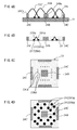
- the conventional example 1 discloses an interposer substrate 200 in which wires are used. An outline of the interposer substrate 200 is described referring to FIG. 9 .
- the interpose substrate 200 comprises a double-surfaced wiring board 100 and an insulation resin layer 141 .
- a land 121 and a terminal 122 for solder bump are electrically connected to each other through a via hole 131 .
- the insulation resin layer 141 is formed on the double-surfaced wiring board 100 .
- An electrical conduction lead 151 a is extended from the land 121 in the insulation resin layer 141 toward a surface of the insulation resin layer 141 .
- a connection terminal 151 b is formed at the distal end of the electrical conduction lead 151 a.
- a double-surfaced wiring board 100 wherein the land 121 and the terminal 122 for solder bump are formed on both surfaces of an insulation substrate 111 , is prepared.
- a wire 151 a is extended from the land 121 of the double-surfaced wiring board 100 at a predetermined angle, and an insulation resin layer 141 is then formed. After the formation of the insulation resin layer 141 , the wire 151 a present on a surface of the insulation resin layer 141 is cut away, and the surface is polished.
- an interposer substrate (substrate for semiconductor package) 200 wherein the electrical conduction lead 151 a is formed in the insulation resin layer 141 and the connection terminal 151 b is formed on the surface of the insulation resin layer 141 , is obtained.
- an inter-land interval is approximately 300 microns at the very most, which fails to meet the level of the miniaturization currently demanded.
- the conventional example 1 is further disadvantageous in that any effective measures for heat release and denoising, which are requirements of an interposer substrate in addition to miniaturization, have not been adopted.
- a main object of the present invention is to provide a fine-pitched interposer substrate.
- an interposer substrate manufacturing process comprises:
- the interposer substrate obtained by the process according to the present invention since the metal wire is provided so as to penetrate the resin-cured material in its thickness direction, an end of the metal wire can be used as a connection electrode for connecting a semiconductor device thereto, while the other end thereof can be used as a land electrode for connecting a mother board thereto.
- a diameter of the metal wire is such an extremely small dimension as approximately 12-25 microns. Therefore, the interposer substrate obtained by the present invention is far more fine-pitched than a conventional interposer substrate.
- the interposer substrate manufacturing process further comprises a fifth step in which a projection, at least the surface of which is made of metal, is formed on the principal surface of the block prior to the first step, wherein
- one of the pair of discretionary points is set on the principal surface and the other is set on the upper surface of the projection in the first step
- the upper-surface portion of the resin-cured material is removed to such an extent that the projection is exposed in the third step
- the block excluding the projection is removed from the resin-cured material in the fourth step.
- the projection can be used as a heat-release path for releasing heat generated in the semiconductor device, so that a temperature of the semiconductor device can be lowered.
- a stable reference electrode can be obtained, which stabilizes electric characteristics, while a stable potential can be obtained when the projection is used as a power supply.
- the interposer substrate manufacturing process further comprises a fifth step in which a projection which is provided with a step portion and at least the surface of which is made of metal is formed on the principal surface of the block prior to the first step, wherein
- one of the pair of discretionary points is set on the uppermost surface of the projection and the other is set on the upper surface of the step portion of the projection or the principal surface in the first step,
- the upper-surface portion of the resin-cured material is removed to such an extent that the projection is exposed in the third step
- the block excluding the projection is removed from the resin-cured material in the fourth step.
- ground terminals or power-supply terminals of the semiconductor device can be intensively provided on the projection, and the number of pins can be thereby reduced.
- a pair of the projections are formed on the principal surface so as to be as close to each other as possible in the fifth step, and the pair of discretionary points are coupled to each other with the metal wire, and the gap between the pair of the projections is filled with a dielectric member in the first step.
- one of the projections can be used as a ground, while the other projection can be used as a power supply.
- a bypass capacitor also called a decoupling capacitor
- noises can be reduced.
- a chip-type electronic component for example, chip capacitor
- a similar effect can be obtained.
- the interposer substrate manufacturing process further comprises a sixth step in which electrodes connected to the metal wire are formed on the surface of the resin-cured material after the fourth step.
- the electrodes can be properly formed and capitad, which improves mountability.
- the used metallic material may seep into the melted solder. This problem, however, can be solved when the electrodes are made of barrier metal (Cr, Ni or the like) by electroless plating.
- a fine-pitched interposer substrate can be obtained.
- various pitches can be considered as a fine pitch, a fine pitch here means approximately 12-25 microns.
- connection electrode for connecting the semiconductor device and the land electrode for connecting the mother board can be connected to each other with a shortest distance therebetween.
- An interposer substrate whose ground potential is stabilized can be obtained.
- An interposer substrate superior in heat releasability can be obtained.
- a dielectric member can be easily provided in the interposer substrate, and the interposer substrate provided with the dielectric member can achieve superior noise characteristics.
- an interposer substrate which is far more fine-pitched than any conventional interposer substrate can be obtained. Moreover, an interposer substrate superior in heat releasability and electric characteristics can be obtained.
- FIGS. 1A-1E are sectional views respectively illustrating an interposer substrate manufacturing process according to a preferred embodiment 1 of the present invention.
- FIG. 2A is a plan view of an interposer substrate manufactured in the manufacturing process according to the preferred embodiment 1.
- FIG. 2B is a bottom view of the interposer substrate manufactured in the manufacturing process according to the preferred embodiment 1.
- FIGS. 3A-3D are sectional views respectively illustrating an interposer substrate manufacturing process according to a preferred embodiment 2 of the present invention.
- FIG. 3E is a plan view of an interposer substrate manufactured in the manufacturing process according to the preferred embodiment 2.
- FIG. 3F is a bottom view of the interposer substrate manufactured in the manufacturing process according to the preferred embodiment 2.
- FIGS. 4A-4B are sectional views respectively illustrating an interposer substrate manufacturing process according to a modified embodiment (1) of the preferred embodiment 2.
- FIG. 4C is a plan view of an interposer substrate manufactured in the manufacturing process according to the modified embodiment (1) of the preferred embodiment 2.
- FIG. 4D is a bottom view of the interposer substrate manufactured in the manufacturing process according to the modified embodiment (1) of the preferred embodiment 2.
- FIGS. 5A-5B are sectional views respectively illustrating an interposer substrate manufacturing process according to a modified embodiment (2) of the preferred embodiment 2.
- FIG. 5C is a plan view of an interposer substrate manufactured in the manufacturing process according to the modified embodiment (2) of the preferred embodiment 2.
- FIG. 5D is a bottom view of the interposer substrate manufactured in the manufacturing process according to the modified embodiment (2) of the preferred embodiment 2.
- FIGS. 6A-6D are sectional views respectively illustrating an interposer substrate manufacturing process according to a preferred embodiment 3 of the present invention.
- FIG. 6E is a plan view of an interposer substrate manufactured in the manufacturing process according to the preferred embodiment 3.
- FIG. 6F is a bottom view of the interposer substrate manufactured in the manufacturing process according to the preferred embodiment 3.
- FIGS. 7A-7C are sectional views respectively illustrating an interposer substrate manufacturing process according to a preferred embodiment 4 of the present invention.
- FIG. 7D is a plan view of an interposer substrate manufactured in the manufacturing process according to the preferred embodiment 4.
- FIG. 7E is a bottom view of the interposer substrate manufactured in the manufacturing process according to the preferred embodiment 4.
- FIG. 8A is a sectional view of an interposer substrate manufactured in a manufacturing process according to a modified embodiment of the preferred embodiment 4.
- FIG. 8B is a plan view of the interposer substrate manufactured in the manufacturing process according to the modified embodiment of the preferred embodiment 4.
- FIG. 8C is a bottom view of the interposer substrate manufactured in the manufacturing process according to the modified embodiment of the preferred embodiment 4.
- FIG. 9 is a sectional view of a conventional interposer substrate.
- a thin metal plate 11 which is an example of a block, is prepared.
- the metal plate 11 is described below using an aluminum plate (A 1 ) as an example.
- the metal plate 11 may be made of a different type of metal, or a plate configured such that the periphery of an insulation material is coated with metal or only a part of the insulation material is coated with metal may be used.
- the metal wire 12 may be an Au wire, an Al wire, a Cu wire or the like. In the present preferred embodiment, an Au wire having the diameter of 12 microns is used.
- One end of the metal wire 12 has a shape 12 a called “ball bond,” the other end has a shape 12 b called “stitch bond.”
- the metal wire 12 is coupled to the metal plate 11 via these shapes 12 a and 12 b (see FIG. 1A ).
- liquid resin (not shown) is applied by a dispenser (not shown) to the principal surface 11 a of the metal substrate 11 to such an extent that the metal wire 12 is dipped therein.
- the liquid resin used here is a material containing epoxy resin as its main ingredient in which silica powder, carbon black and the like are dispersed.
- resin for glob-top is applied; however, a method of the application and physical properties of the applied resin are not particularly limited.
- the applied liquid resin is heated, for example, at 150° C. for approximately one hour, so that a resin-cured material 13 is obtained.
- the resin is cured by the heat treatment; however, the irradiation of light and the heat treatment may be combined to cure the resin (see FIG. 1B ).
- the upper-surface portion of the resin-cured material 13 is polished. More specifically, a SiC sand paper having appropriate particle sizes (not shown) is prepared, and the upper-surface portion of the resin-cured material 13 is thereby polished to be removed so that the upper surface 13 a of the resin-cured material 13 will be in parallel with the metal plate 11 . In the polishing process, an intermediate portion 12 c of the metal wire 12 having a bow-like shape or any other curved shape is removed together with the upper-surface portion of the resin-cured material 13 (see FIG. 1C ).
- first and second wire portions 12 d and 12 e at both ends of the metal wire 12 remain in the post-polishing resin-cured material 13 .
- the ball bond shape 12 a is located at one end of the second wire portion 12 d (at the end portion on the side of the metal plate 11 ), while the stitch bond shape 12 b is located at one end of the second wire portion 12 e (at the end portion on the side of the metal plate 11 ).
- the other end of the first wire portion 12 d is exposed out of a polished surface 13 a ′ of the resin-cured material 13 .
- the other end of the second wire portion 12 e is exposed out of the polished surface 13 a ′ of the resin-cured material 13 .
- the polished surface 13 a ′ of the resin-cured material 13 is referred to as one principal surface 13 a ′ of the resin-cured material 13 .
- a cutting process may be adopted.
- the resin-cured material 13 is cut away together with the intermediate portion 12 c of the metal wire 12 by, for example, a diamond cutter so that the polished surface 13 a ′ of the resin-cured material 13 will be in parallel with the metal plate 11 .
- the metal plate 11 is removed from the resin-cured material 13 . Accordingly, the other ends of the first and second wire portions 12 d and 12 e on the other principal surface 13 b of the resin-cured material 13 (the ball bond shape 12 a and the stitch bond shape 12 b are provided at these other ends) are exposed out of the resin-cured material 13 .
- silicon grease is applied in advance to the metal plate 11 except for the sections where the metal wire 12 is bonded.
- the metal plate 11 is removed by inserting a metal plate having a thickness of approximately 20 microns into the interface between the metal plate 11 and the resin-cured material 13 .
- the metal plate 11 may be polished or cut away to be removed (see FIG. 1D ).
- electrodes 14 and 15 are properly formed and aligned.
- An example of the formation process is described below. Thin Cu plating is formed on the principal surfaces 13 a ′ and 13 b of the resin-cured material 13 by electroless plating, and the Cu plating is thickened by electroplating, so that electrode layers (not shown) are formed. Then, any unnecessary portions in the formed electrode layers are etched to be removed, so that the electrodes 14 and 15 are formed.
- the formation process can solve the problem that the electrodes are uneven in size or not aligned neatly when the metal wire alone is used. In the case where it is unnecessary for electrodes to be formed or aligned with a very high accuracy, the formation process adopted in this description can be omitted.
- the interposer substrate thus obtained is illustrated in FIG. 1E .
- the metal plate electrode 14 serves as a connection electrode for mounting a semiconductor device, while the metal plate electrode 15 serves as a land electrode for mounting a mother board.
- FIGS. 2A and 2B illustrate the layout of the electrodes viewed from the upper surface and the lower surface of the interposer substrate.
- a reference symbol 14 a (or 15 a ) is assigned to the metal plate electrode at a right-side upper end of the substrate, and then, reference symbols up to 14 t (or 15 t ) are assigned to the respective metal plate electrodes clockwise.
- One of routes through which the metal wire 12 extends is a route 15 a - 14 a - 14 k - 15 k . Below are listed the rest of the routes:
- Au is used as the metal wire 12 . Therefore, when the interposer substrate is connected to the semiconductor device or the mother board by means of solder, the used material seeps into the melted solder.
- barrier metal such as Ni or Cr is preferably formed on the electrodes the electroless plating.
- the interposer substrate thus obtained is approximately 20-micron-pitched, far more fine-pitched than any conventional interposer substrate.
- the interposer substrate when used in electronic devices, can greatly contribute to the miniaturization of the electronic devices.
- a preferred embodiment 2 of the present invention is described referring to FIGS. 3A-3F .
- a metal plate 21 which is an example of a block, is prepared.
- a projection 24 projecting in a thickness direction thereof and constituting a filler member is formed in advance.
- the metal plate 21 is made of, for example, aluminum (Al).
- the metal plate 21 provided with the projection may be separate metal blocks bonded to each other, or the projection 24 may be formed on the metal plate 21 when the metal plate 21 is formed.
- a discretionary point on a principal surface 21 a of the metal plate 21 and a discretionary point on the upper surface 24 a of the projection 24 are coupled to each other with a metal wire 22 having a length larger than a distance between the two discretionary points and having a bow-like shape or any other curved shape by an all-purpose wire boding device. It is preferable that the metal wire 22 is ball-bonded to the principal surface 21 a , and then stitch-bonded to the upper surface 24 a of the projection 24 . The metal wire 22 is thus bonded because the wire diameter at the bonding section is large when the metal wire 22 is ball-bonded to the principal surface 21 a and can be directly used as the land for the wide-pitched mother board (see FIG. 3A ).
- a shape 22 a called ball bond is formed at one end of the metal wire 22
- a shape 22 b called stitch bond is formed at the other end thereof.
- the metal wire 22 is coupled to the metal plate 21 and the projection 24 via the shapes 22 a and 22 b.
- liquid resin is applied to the principal surface 21 a of the metal plate 21 by a dispenser to such an extent that the metal wire 22 is dipped therein.
- the applied liquid resin is, for example, heated at 150° C. for one hour to be cured, so that a resin-cured material 23 is obtained (see FIG. 3B ).
- the upper-surface portion of the resin-cured material 23 is polished. More specifically, a SiC sand paper having appropriate particle sizes (not shown) is prepared, and the upper-surface portion of the resin-cured material 23 is thereby polished to be removed so that the upper surface 23 a of the resin-cured material 23 will be in parallel with the metal plate 21 .
- the resin-cured material 23 is removed until the upper surface 24 a of the projection 24 is exposed.
- an end portion 22 c of the metal wire 22 having a bow-like shape or any other curved shape is removed together with the upper-surface portion of the resin-cured material 23 (see FIG. 1C ).
- a wire portion 22 d at the other end of the metal wire 2 remains in the post-polishing resin-cured material 23 .
- the ball bond shape 22 a is located at one end of the wire portion 22 d (at the end portion on the side of the metal plate 21 ).
- the other end 22 b of the wire portion 22 d is exposed out of a polished surface 23 a ′ of the resin-cured material 23 .
- the polished surface 23 a ′ of the resin-cured material 23 is referred to as one principal surface 23 a ′ of the resin-cured material 23 .
- the metal plate 21 (not including the projection 24 ) is removed from the resin-cured material 23 according to a method similar to that of the preferred embodiment 1. Accordingly, the one end of the wire portion 22 d on the other principal surface 23 b of the resin-cured material 23 (where the ball bond shape 22 a is provided) is exposed out of the resin-cured material 23 , and a lower surface 24 b of the projection 24 is exposed out of the resin-cured material 23 . As a result of these steps, an interposer substrate can be obtained (see FIGS. 3D-3F ).
- the projection 24 is provided in the resin-cured material 23 so as to penetrate therethrough in a thickness direction thereof, and the upper and lower surfaces 24 a and 24 b of the projection 24 are exposed out of the resin-cured material 23 .
- the projection 24 can be used as a heat-release path.
- an interposer substrate having a high heat releasability can be obtained.
- the projection 24 is used not only for heat release but also, for example, as a ground, a semiconductor package having a high electric stability wherein a reference potential is stabilized can be provided.
- the projection 24 can be used as a power supply, in which case an effect similar to the effect obtained when the projection 24 is used as the ground can be obtained.
- the projection 24 when the projection 24 is used as the ground or power supply, it is necessary to connect the upper surface 24 a of the projection 24 (on which the semiconductor device is mounted) to power supply or ground pins of the semiconductor device. After that, the connection and land electrodes are formed and aligned on an as needed basis by, for example, electroless plating, electroplating, etching and the like.
- the land electrode for mounting the mother board can be provided at any discretionary position, which is described referring to FIGS. 4A-4D .
- a plurality of projections 24 C and 24 B are provided on the principal surface 21 a of the metal plate 21 .
- a first metal wire 22 c is provided so as to extend from the upper surface 21 a of the metal plate 21 to the upper surface 24 Ca of the projection 24 C, while a second metal wire 22 B is provided so as to extend from the upper surface 21 a to the upper surface 24 Ba of the projection 24 B.
- the first and second metal wires 22 C and 22 B are ball-bonded to the principal surface 21 a , and then stitch-bonded to the upper surfaces 24 Ca and 24 Ba of the projections 24 C and 24 B. It appears in the drawing that the first metal wiring 22 C and the second metal wire 22 B intersect; however, they are actually apart in a depth direction of the drawing.
- Ball bonding shapes 25 of the first and second metal wires 22 B and 22 C provided on the principal surface 21 a serve as land electrodes as a result of the subsequent steps.
- a formation pitch of the ball bonding shape 25 is arbitrarily set depending on a layout pitch of the land electrode.
- a layout pitch of the land electrode 25 of the interposer substrate can be set to either fan-in or fan-out depending on the formation pitch of the ball bonding shape.
- a reference symbol 22 Cd in the drawing denotes the first metal wire still remaining after the resin-cured material 23 is polished, while a reference symbol Bd denotes the second metal wire still remaining after the resin-cured material 23 is polished.
- a reference symbol 25 ( 22 Cd) denotes a land electrode connected to the first metal wire 22 Cd, while 25 (Bd) denotes a land electrode connected to the second metal wire Bd.
- first and second metal wires 22 D and 22 E respectively having different loop shapes (shapes having different lengths) are provided so as to extend from the principal surface 21 a of the metal plate 21 comprising the projection 24 to the upper surface 24 a of the projection 24 .
- the first metal wire 22 D is long and has an acutely bent shape.
- the second metal wire 22 E is short and has a moderately bent shape. It appears in the drawing that the first metal wire 22 D and the second metal wire 22 E intersect; however, they are actually apart in a depth direction of the drawing.
- a reference symbol 22 Dd denotes the first metal wire still remaining after the resin-cured material 23 is polished
- a reference symbol 22 Ed denotes the second metal wire still remaining after the resin-cured material 23 is polished
- a reference symbol 25 ( 22 Dd) denotes a land electrode connected to the first metal wire 22 Dd
- a reference symbol 25 ( 22 Ed) denotes a land electrode connected to the second metal wire 22 Ed.
- the metal wires 22 D and 22 E having the described shapes are provided, and liquid resin is applied to the metal plate 21 so as to cover the metal wires 22 D and 22 E and then cured. After that, the upper-surface portion of the resin-cured material 23 thereby obtained is polished, and the metal plate 21 (not including the projection 24 ) is removed from the resin-cured material 23 . As a result, an interposer substrate illustrated in FIGS. 5B-5D can be obtained.
- the land electrode 25 can be formed at any discretionary position as far as the position is on an outer side than the connection electrode for mounting the semiconductor device.
- the land electrodes for mounting the mother board can be provided at any discretionary positions of the interposer substrate.
- the interposer substrate thus obtained exerts, in addition to the effects described in the preferred embodiment 1, the following effects.
- Metal having a high thermal conductivity can constitute the projection (filler member) 24 embedded in the resin-cured material 23 . Therefore, heat generated in the semiconductor device can be efficiently transferred to the mother board.
- the projection (filler member) 24 When the projection (filler member) 24 is used as a ground, a reference potential is stabilized, and high electric stability can be obtained.
- the entire body of the projection (filler member) 24 is made of metal; however, a similar effect can be exerted as far as at least the surface thereof is made of metal.
- a preferred embodiment 3 of the present invention is described referring to FIGS. 6A-6F .
- a metal plate 31 which is an example of a block, is prepared.
- a projection 34 provided with a step portion 34 a in advance in a plate-thickness direction is formed on a principal surface 31 a of the metal plate 31 .
- the projection 34 which is provided with the step portion 34 a , comprises an uppermost surface 34 b and an upper surfaces 34 c of the step portion.
- the metal plate 21 is made of, for example, aluminum (Al).
- the uppermost surface 34 b and the upper surfaces 34 c of the step portions of the projection 34 on the metal plate 31 are coupled to each other, and the uppermost surface 34 b and a discretionary point of the principal surface 31 a of the metal plate 31 are coupled to each other with metal wires 32 having a bow-like shape or any other curved shape by an all-purpose wire boding device (see FIG. 6A ). It appears in the drawing that the metal wires 32 intersect; however, they are actually apart in a depth direction of the drawing.
- liquid resin is applied to the principal surface 31 b of the metal plate 31 by a dispenser to such an extent that the metal wires 32 are dipped therein.
- the applied liquid resin is, for example, heated at 150° C. for one hour to be cured, so that a resin-cured material 33 is obtained (see FIG. 6B ).
- the upper-surface portion of the resin-cured material 33 is polished. More specifically, the upper-surface portion of the resin-cured material 33 is polished to be removed so that the upper surface 33 a of the resin-cured material 33 will be in parallel with the principal surface 31 a of the metal plate 31 (see FIG. 6C ).
- the resin-cured material 33 is polished until the uppermost surface 34 b of the projection 34 is exposed.
- one-end portions 32 c of the metal wires 32 are removed together with the upper-surface portion of the resin-cured material 33 .
- a wire portion 32 d at the other end of the metal wire 32 remains in the post-polishing resin-cured material 33 .
- a ball bond shape 32 a is located at one end of the wire portion 32 d (end portion on the side of the metal plate 31 ).
- the other end 32 b of the wire portion 32 d is exposed out of a polished surface (one principal surface) 33 a ′ of the resin-cured material 33 .
- the ball bond shape 32 a serves as a land electrode for mounting a mother board, while the other end 32 b of the wire portion 32 d serves as a connection electrode for mounting a semiconductor device.
- the ball bond shape 32 a exposed out of the other principal surface 33 b of the resin-cured material 33 serves as a land electrode for receiving and transmitting a signal with respect to the mother board.
- Some of the plurality of ball bond shapes 32 a abut the upper surfaces 34 c of the step portions and are thereby connected to the projection 34 . Since the ball bond shapes 32 a are thus connected thereto, the projection 34 can serve as a land electrode for a power supply or ground of the semiconductor device.
- step portions 32 a are provided in the projection 34 when the ball bond shapes 32 a are provided on the projection 34 .
- the ball bond shapes 32 a can be formed in the projection 34 by the all-purpose wire bonding device.
- the metal plate 31 (not including the projection 34 ) is removed from the resin-cured material 33 according to a method similar to that of the preferred embodiments 1 and 2, and an interpose substrate can be obtained (see FIGS. 6D-6F ).
- the interposer substrate thus obtained exerts, in addition to the effects described in the preferred embodiments 1 and 2, the following effects.
- the power supply or ground can be intensively provided on the projection 34 on the interposer substrate, the number of pins can be reduced when the semiconductor device is packaged. Accordingly, a level of designing difficulty is significantly lessened, which reduces a designing period.
- a preferred embodiment 4 of the present invention is an application of the preferred embodiment 3.
- an interposer provided with a capacitor therein can be manufactured.
- FIGS. 7A-7E wherein the structural components and the constitutions already described in the preferred embodiments 1-3 will not be repeatedly described.
- a metal plate 41 which is an example of a block, is prepared.
- first and second projections 44 A and 44 B each having a step portion 44 a are formed in advance in a plate-thickness direction.
- the first and second projections 44 A and 44 B respectively have a side surface on which the step portion 44 a is formed, and a side surface opposite thereto on which the step portion 44 a is not formed.
- the first and second projections 44 A and 44 B are provided with each side surface on which the step portion 44 a is not formed facing each other with a distance therebetween; however, they are placed as close to each other as possible.
- a discretionary point on the uppermost surface 44 b of the first projection 44 A and a discretionary point on a principal surface 41 a of the metal plate 41 are coupled to each other with a metal wire 42 A; a discretionary point on the uppermost surface 44 b of the first projection 44 A and the upper surface 44 c of the step portion of the first projection 44 A are coupled to each other with a metal wire 42 B; and a discretionary point on the uppermost surface 44 b of the second projection 44 B and the upper surface 44 c of the step portion of the second projection 44 B are coupled to each other with a metal wire 42 C (see FIG. 6A ).
- an all-purpose wire bonding device is used. It appears in the drawing that the metal wire 42 A and the metal wire 42 B intersect; however, they are actually apart in a depth direction of the drawing.
- the first projection 44 A is connected to a power supply pin of a semiconductor device through the metal wire 42 B as a result of the processing described later, while the second projection 44 B is connected to a ground pin of the semiconductor device through the metal wire 42 C as a result of the processing described later.
- a dielectric paste is applied to the gap between the first projection 44 A and the second projection 44 B and heated at 150° C. for approximately one hour to be cured, so that a dielectric layer 46 is formed.
- the dielectric paste is used, for example, epoxy resin in which titanic acid barium particles are dispersed (see FIG. 7B ).
- liquid resin is applied to the metal plate 41 so as to cover the metal wires 42 A, 42 B and 42 C and thereafter cured. Then, the resin-cured material 43 thereby obtained is polished, and the metal plate 41 (not including the projections 44 ) is removed.
- polishing and removal processes which are similar to those described in the preferred embodiments 1 and 2, is omitted.
- an interposer substrate illustrated in FIG. 7C-7E can be obtained.
- the first projection 44 A, dielectric layer 46 and second projection 44 B constitute a capacitor.
- the surfaces may be polished to be roughened, or anodic oxidation adopted in an aluminum electrolytic capacitor or the like may be performed.
- an alternate current is applied using the metal plate 41 as a feeder layer, and the side surfaces of the first and second projections 44 A and 44 B are electrolytically etched in an electrolytic solution containing hydrochloric acid as a main ingredient thereof to be thereby roughened.
- a voltage is applied to the metal plate 41 (feeder layer) in a neutral electrolytic solution, so that the side surfaces of the first and second projections 44 A and 44 B are anodically oxidated.
- This anodic oxidation further roughens the side surfaces of the first and second projections 44 A and 44 B, and forms an oxide film on these side surfaces.
- the applied voltage is, for example, approximately 30-100 V, and a film thickness of the formed oxide film is, for example, approximately 20-120 nm.
- engaging step portions 44 e and 44 e are respectively formed on the side surfaces 44 d and 44 d of the first and second projections 44 A and 44 B facing each other, and a chip capacitor 47 is placed between the engaging step portions 44 e and 44 e as illustrated in FIGS. 8A-8C .
- a depth of the engaging step portions 44 e and 44 e is set to be larger than a height of the chip capacitor 47 . Accordingly, the chip capacitor 47 is housed therein without protruding upward from the engaging step portions 44 e and 44 e .
- the chip capacitor 47 is connected to the first and second projections 44 A and 44 B at bottom portions of the engaging step portions 44 e and 44 e.
- liquid resin is applied to the metal plate (not shown) so as to cover the metal wires 42 A, 42 B and 42 C and the chip capacitor 47 and thereafter cured. Then, a resin-cured material 43 thereby obtained is polished, and the metal plate (not including the projections 44 A and 44 B) is removed.
- the chip capacitor 47 can be used as a bypass capacitor.
- a bonding material used when the chip capacitor 47 is mounted on the first projection 44 A and the second projection 44 B may be solder or a conducive paste in which metal such as Ag is dispersed. It is, however, necessary to previously form a resist film on the metal plate 41 when solder is used.
- the interposer substrate thus obtained has the effect of removing high electromagnetic noise in addition to the effects described earlier.
Landscapes
- Engineering & Computer Science (AREA)
- Manufacturing & Machinery (AREA)
- Microelectronics & Electronic Packaging (AREA)
- Encapsulation Of And Coatings For Semiconductor Or Solid State Devices (AREA)
- Structures For Mounting Electric Components On Printed Circuit Boards (AREA)
- Insulated Metal Substrates For Printed Circuits (AREA)
Abstract
Description
Claims (7)
Applications Claiming Priority (2)
| Application Number | Priority Date | Filing Date | Title |
|---|---|---|---|
| JP2008165425A JP5511155B2 (en) | 2008-06-25 | 2008-06-25 | Interposer substrate and manufacturing method thereof |
| JP2008-165425 | 2008-06-25 |
Publications (2)
| Publication Number | Publication Date |
|---|---|
| US20090321124A1 US20090321124A1 (en) | 2009-12-31 |
| US8344264B2 true US8344264B2 (en) | 2013-01-01 |
Family
ID=41446037
Family Applications (1)
| Application Number | Title | Priority Date | Filing Date |
|---|---|---|---|
| US12/489,818 Expired - Fee Related US8344264B2 (en) | 2008-06-25 | 2009-06-23 | Semiconductor device and manufacturing process thereof |
Country Status (2)
| Country | Link |
|---|---|
| US (1) | US8344264B2 (en) |
| JP (1) | JP5511155B2 (en) |
Families Citing this family (5)
| Publication number | Priority date | Publication date | Assignee | Title |
|---|---|---|---|---|
| FR2957191B1 (en) * | 2010-03-04 | 2012-12-28 | Tronic S Microsystems | ELECTRIC INTERCONNECTION SUPPORT STRUCTURE FOR INTEGRATED CIRCUITS, AND METHOD FOR MANUFACTURING SAME |
| JP5928974B2 (en) * | 2011-10-19 | 2016-06-01 | 住友電気工業株式会社 | Reactor, converter, and power converter |
| US8835228B2 (en) * | 2012-05-22 | 2014-09-16 | Invensas Corporation | Substrate-less stackable package with wire-bond interconnect |
| JP6108164B2 (en) * | 2012-11-07 | 2017-04-05 | 日本電産株式会社 | Solder joint structure and solder joint method |
| JP2016139730A (en) * | 2015-01-28 | 2016-08-04 | 株式会社東芝 | Electronic device and method of manufacturing substrate |
Citations (4)
| Publication number | Priority date | Publication date | Assignee | Title |
|---|---|---|---|---|
| US5309324A (en) * | 1991-11-26 | 1994-05-03 | Herandez Jorge M | Device for interconnecting integrated circuit packages to circuit boards |
| US6265673B1 (en) * | 1996-07-09 | 2001-07-24 | Matsushita Electric Industrial Co., Ltd. | Semiconductor element-mounting board and semiconductor device |
| JP2003152133A (en) | 2001-11-12 | 2003-05-23 | Toppan Printing Co Ltd | Semiconductor package substrate and method of manufacturing the same |
| US6613979B1 (en) * | 1995-01-06 | 2003-09-02 | Quell Corporation | Electrical circuit suspension system |
Family Cites Families (3)
| Publication number | Priority date | Publication date | Assignee | Title |
|---|---|---|---|---|
| AU4160096A (en) * | 1994-11-15 | 1996-06-06 | Formfactor, Inc. | Probe card assembly and kit, and methods of using same |
| JP2809385B2 (en) * | 1994-11-29 | 1998-10-08 | 信越ポリマー株式会社 | Semiconductor element connection wiring board and semiconductor element connection structure |
| JPH11311655A (en) * | 1998-04-30 | 1999-11-09 | Mitsubishi Electric Corp | Semiconductor evaluation equipment |
-
2008
- 2008-06-25 JP JP2008165425A patent/JP5511155B2/en not_active Expired - Fee Related
-
2009
- 2009-06-23 US US12/489,818 patent/US8344264B2/en not_active Expired - Fee Related
Patent Citations (4)
| Publication number | Priority date | Publication date | Assignee | Title |
|---|---|---|---|---|
| US5309324A (en) * | 1991-11-26 | 1994-05-03 | Herandez Jorge M | Device for interconnecting integrated circuit packages to circuit boards |
| US6613979B1 (en) * | 1995-01-06 | 2003-09-02 | Quell Corporation | Electrical circuit suspension system |
| US6265673B1 (en) * | 1996-07-09 | 2001-07-24 | Matsushita Electric Industrial Co., Ltd. | Semiconductor element-mounting board and semiconductor device |
| JP2003152133A (en) | 2001-11-12 | 2003-05-23 | Toppan Printing Co Ltd | Semiconductor package substrate and method of manufacturing the same |
Also Published As
| Publication number | Publication date |
|---|---|
| JP2010010248A (en) | 2010-01-14 |
| JP5511155B2 (en) | 2014-06-04 |
| US20090321124A1 (en) | 2009-12-31 |
Similar Documents
| Publication | Publication Date | Title |
|---|---|---|
| TWI358973B (en) | ||
| TWI529832B (en) | Module and manufacturing method thereof | |
| US8178957B2 (en) | Electronic component device, and method of manufacturing the same | |
| JP2004343030A (en) | Printed circuit board, method of manufacturing the same, and circuit module provided with the printed circuit board | |
| KR20020022527A (en) | Semiconductor device and semiconductor module | |
| KR100551576B1 (en) | Semiconductor device and method of producing the same | |
| CN109390293B (en) | Semiconductor packaging device and manufacturing method thereof | |
| US8344264B2 (en) | Semiconductor device and manufacturing process thereof | |
| JP5272922B2 (en) | Semiconductor device and manufacturing method thereof | |
| JP4498378B2 (en) | Substrate and manufacturing method thereof, circuit device and manufacturing method thereof | |
| US10211119B2 (en) | Electronic component built-in substrate and electronic device | |
| US12494446B2 (en) | Package structures and methods of manufacturing the same | |
| JP5173758B2 (en) | Manufacturing method of semiconductor package | |
| JP2016039290A (en) | Printed wiring board and semiconductor package | |
| JP6397313B2 (en) | Printed wiring board and semiconductor package | |
| US20160211239A1 (en) | Package Having Substrate With Embedded Metal Trace Overlapped by Landing Pad | |
| CN100437959C (en) | Component mounting method and body with component mounted | |
| CN1791311B (en) | Method of manufacturing a circuit substrate and method of manufacturing an electronic parts packaging structure | |
| JP2016039302A (en) | Printed wiring board and manufacturing method of the same, and semiconductor package | |
| CN104637913A (en) | Electronic component module and manufacturing method thereof | |
| JP4494249B2 (en) | Semiconductor device | |
| CN117641723A (en) | A printed circuit board | |
| KR101128999B1 (en) | Manufacturing method for chip package and chip package produced by the method | |
| JP4168494B2 (en) | Manufacturing method of semiconductor device | |
| CN100446244C (en) | Semiconductor chip package and manufacturing method thereof |
Legal Events
| Date | Code | Title | Description |
|---|---|---|---|
| AS | Assignment |
Owner name: PANASONIC CORPORATION, JAPAN Free format text: ASSIGNMENT OF ASSIGNORS INTEREST;ASSIGNORS:KUMANO, YUTAKA;IWAKI, HIDEKI;OGURA, TETSUYOSHI;AND OTHERS;REEL/FRAME:022922/0707 Effective date: 20090619 |
|
| STCF | Information on status: patent grant |
Free format text: PATENTED CASE |
|
| FEPP | Fee payment procedure |
Free format text: PAYOR NUMBER ASSIGNED (ORIGINAL EVENT CODE: ASPN); ENTITY STATUS OF PATENT OWNER: LARGE ENTITY |
|
| FEPP | Fee payment procedure |
Free format text: PAYER NUMBER DE-ASSIGNED (ORIGINAL EVENT CODE: RMPN); ENTITY STATUS OF PATENT OWNER: LARGE ENTITY Free format text: PAYOR NUMBER ASSIGNED (ORIGINAL EVENT CODE: ASPN); ENTITY STATUS OF PATENT OWNER: LARGE ENTITY |
|
| FPAY | Fee payment |
Year of fee payment: 4 |
|
| FEPP | Fee payment procedure |
Free format text: MAINTENANCE FEE REMINDER MAILED (ORIGINAL EVENT CODE: REM.); ENTITY STATUS OF PATENT OWNER: LARGE ENTITY |
|
| LAPS | Lapse for failure to pay maintenance fees |
Free format text: PATENT EXPIRED FOR FAILURE TO PAY MAINTENANCE FEES (ORIGINAL EVENT CODE: EXP.); ENTITY STATUS OF PATENT OWNER: LARGE ENTITY |
|
| STCH | Information on status: patent discontinuation |
Free format text: PATENT EXPIRED DUE TO NONPAYMENT OF MAINTENANCE FEES UNDER 37 CFR 1.362 |
|
| FP | Lapsed due to failure to pay maintenance fee |
Effective date: 20210101 |