US8339424B2 - Emission driver and organic light emitting display using the same - Google Patents
Emission driver and organic light emitting display using the same Download PDFInfo
- Publication number
- US8339424B2 US8339424B2 US12/380,464 US38046409A US8339424B2 US 8339424 B2 US8339424 B2 US 8339424B2 US 38046409 A US38046409 A US 38046409A US 8339424 B2 US8339424 B2 US 8339424B2
- Authority
- US
- United States
- Prior art keywords
- transistor
- power supply
- light emitting
- coupled
- input terminal
- Prior art date
- Legal status (The legal status is an assumption and is not a legal conclusion. Google has not performed a legal analysis and makes no representation as to the accuracy of the status listed.)
- Active, expires
Links
Images


Classifications
-
- G—PHYSICS
- G09—EDUCATION; CRYPTOGRAPHY; DISPLAY; ADVERTISING; SEALS
- G09G—ARRANGEMENTS OR CIRCUITS FOR CONTROL OF INDICATING DEVICES USING STATIC MEANS TO PRESENT VARIABLE INFORMATION
- G09G3/00—Control arrangements or circuits, of interest only in connection with visual indicators other than cathode-ray tubes
- G09G3/20—Control arrangements or circuits, of interest only in connection with visual indicators other than cathode-ray tubes for presentation of an assembly of a number of characters, e.g. a page, by composing the assembly by combination of individual elements arranged in a matrix no fixed position being assigned to or needed to be assigned to the individual characters or partial characters
- G09G3/22—Control arrangements or circuits, of interest only in connection with visual indicators other than cathode-ray tubes for presentation of an assembly of a number of characters, e.g. a page, by composing the assembly by combination of individual elements arranged in a matrix no fixed position being assigned to or needed to be assigned to the individual characters or partial characters using controlled light sources
- G09G3/30—Control arrangements or circuits, of interest only in connection with visual indicators other than cathode-ray tubes for presentation of an assembly of a number of characters, e.g. a page, by composing the assembly by combination of individual elements arranged in a matrix no fixed position being assigned to or needed to be assigned to the individual characters or partial characters using controlled light sources using electroluminescent panels
- G09G3/32—Control arrangements or circuits, of interest only in connection with visual indicators other than cathode-ray tubes for presentation of an assembly of a number of characters, e.g. a page, by composing the assembly by combination of individual elements arranged in a matrix no fixed position being assigned to or needed to be assigned to the individual characters or partial characters using controlled light sources using electroluminescent panels semiconductive, e.g. using light-emitting diodes [LED]
- G09G3/3208—Control arrangements or circuits, of interest only in connection with visual indicators other than cathode-ray tubes for presentation of an assembly of a number of characters, e.g. a page, by composing the assembly by combination of individual elements arranged in a matrix no fixed position being assigned to or needed to be assigned to the individual characters or partial characters using controlled light sources using electroluminescent panels semiconductive, e.g. using light-emitting diodes [LED] organic, e.g. using organic light-emitting diodes [OLED]
- G09G3/3266—Details of drivers for scan electrodes
-
- G—PHYSICS
- G09—EDUCATION; CRYPTOGRAPHY; DISPLAY; ADVERTISING; SEALS
- G09G—ARRANGEMENTS OR CIRCUITS FOR CONTROL OF INDICATING DEVICES USING STATIC MEANS TO PRESENT VARIABLE INFORMATION
- G09G3/00—Control arrangements or circuits, of interest only in connection with visual indicators other than cathode-ray tubes
- G09G3/20—Control arrangements or circuits, of interest only in connection with visual indicators other than cathode-ray tubes for presentation of an assembly of a number of characters, e.g. a page, by composing the assembly by combination of individual elements arranged in a matrix no fixed position being assigned to or needed to be assigned to the individual characters or partial characters
- G09G3/22—Control arrangements or circuits, of interest only in connection with visual indicators other than cathode-ray tubes for presentation of an assembly of a number of characters, e.g. a page, by composing the assembly by combination of individual elements arranged in a matrix no fixed position being assigned to or needed to be assigned to the individual characters or partial characters using controlled light sources
- G09G3/30—Control arrangements or circuits, of interest only in connection with visual indicators other than cathode-ray tubes for presentation of an assembly of a number of characters, e.g. a page, by composing the assembly by combination of individual elements arranged in a matrix no fixed position being assigned to or needed to be assigned to the individual characters or partial characters using controlled light sources using electroluminescent panels
- G09G3/32—Control arrangements or circuits, of interest only in connection with visual indicators other than cathode-ray tubes for presentation of an assembly of a number of characters, e.g. a page, by composing the assembly by combination of individual elements arranged in a matrix no fixed position being assigned to or needed to be assigned to the individual characters or partial characters using controlled light sources using electroluminescent panels semiconductive, e.g. using light-emitting diodes [LED]
-
- G—PHYSICS
- G11—INFORMATION STORAGE
- G11C—STATIC STORES
- G11C19/00—Digital stores in which the information is moved stepwise, e.g. shift registers
- G11C19/18—Digital stores in which the information is moved stepwise, e.g. shift registers using capacitors as main elements of the stages
- G11C19/182—Digital stores in which the information is moved stepwise, e.g. shift registers using capacitors as main elements of the stages in combination with semiconductor elements, e.g. bipolar transistors, diodes
- G11C19/184—Digital stores in which the information is moved stepwise, e.g. shift registers using capacitors as main elements of the stages in combination with semiconductor elements, e.g. bipolar transistors, diodes with field-effect transistors, e.g. MOS-FET
-
- H—ELECTRICITY
- H05—ELECTRIC TECHNIQUES NOT OTHERWISE PROVIDED FOR
- H05B—ELECTRIC HEATING; ELECTRIC LIGHT SOURCES NOT OTHERWISE PROVIDED FOR; CIRCUIT ARRANGEMENTS FOR ELECTRIC LIGHT SOURCES, IN GENERAL
- H05B33/00—Electroluminescent light sources
- H05B33/12—Light sources with substantially two-dimensional radiating surfaces
-
- G—PHYSICS
- G09—EDUCATION; CRYPTOGRAPHY; DISPLAY; ADVERTISING; SEALS
- G09G—ARRANGEMENTS OR CIRCUITS FOR CONTROL OF INDICATING DEVICES USING STATIC MEANS TO PRESENT VARIABLE INFORMATION
- G09G2300/00—Aspects of the constitution of display devices
- G09G2300/08—Active matrix structure, i.e. with use of active elements, inclusive of non-linear two terminal elements, in the pixels together with light emitting or modulating elements
- G09G2300/0809—Several active elements per pixel in active matrix panels
- G09G2300/0842—Several active elements per pixel in active matrix panels forming a memory circuit, e.g. a dynamic memory with one capacitor
- G09G2300/0861—Several active elements per pixel in active matrix panels forming a memory circuit, e.g. a dynamic memory with one capacitor with additional control of the display period without amending the charge stored in a pixel memory, e.g. by means of additional select electrodes
-
- G—PHYSICS
- G09—EDUCATION; CRYPTOGRAPHY; DISPLAY; ADVERTISING; SEALS
- G09G—ARRANGEMENTS OR CIRCUITS FOR CONTROL OF INDICATING DEVICES USING STATIC MEANS TO PRESENT VARIABLE INFORMATION
- G09G2310/00—Command of the display device
- G09G2310/02—Addressing, scanning or driving the display screen or processing steps related thereto
- G09G2310/0243—Details of the generation of driving signals
- G09G2310/0245—Clearing or presetting the whole screen independently of waveforms, e.g. on power-on
-
- G—PHYSICS
- G09—EDUCATION; CRYPTOGRAPHY; DISPLAY; ADVERTISING; SEALS
- G09G—ARRANGEMENTS OR CIRCUITS FOR CONTROL OF INDICATING DEVICES USING STATIC MEANS TO PRESENT VARIABLE INFORMATION
- G09G2310/00—Command of the display device
- G09G2310/02—Addressing, scanning or driving the display screen or processing steps related thereto
- G09G2310/0264—Details of driving circuits
- G09G2310/0286—Details of a shift registers arranged for use in a driving circuit
-
- G—PHYSICS
- G09—EDUCATION; CRYPTOGRAPHY; DISPLAY; ADVERTISING; SEALS
- G09G—ARRANGEMENTS OR CIRCUITS FOR CONTROL OF INDICATING DEVICES USING STATIC MEANS TO PRESENT VARIABLE INFORMATION
- G09G2310/00—Command of the display device
- G09G2310/06—Details of flat display driving waveforms
- G09G2310/061—Details of flat display driving waveforms for resetting or blanking
- G09G2310/063—Waveforms for resetting the whole screen at once
-
- G—PHYSICS
- G09—EDUCATION; CRYPTOGRAPHY; DISPLAY; ADVERTISING; SEALS
- G09G—ARRANGEMENTS OR CIRCUITS FOR CONTROL OF INDICATING DEVICES USING STATIC MEANS TO PRESENT VARIABLE INFORMATION
- G09G2330/00—Aspects of power supply; Aspects of display protection and defect management
- G09G2330/02—Details of power systems and of start or stop of display operation
- G09G2330/026—Arrangements or methods related to booting a display
Definitions
- the field relates to an emission driver and an organic light emitting display using the same, and more particularly to an emission driver and an organic light emitting display using the same for supplying a light emitting control signal to a light emitting control line.
- the flat panel display can take the form of, for example, a liquid crystal display, a field emission display, a plasma display panel and an organic light emitting display, etc.
- the organic light emitting display displays an image using an organic light emitting diode (OLED) generating light by recombination of electrons and holes.
- OLED organic light emitting diode
- the organic light emitting display has quick response speed and is driven with low power consumption.
- a general organic light emitting display supplies current corresponding to data signals to an organic light emitting diode using driving transistors formed in pixels to allow the organic light emitting diode to generate light.
- Such a conventional organic light emitting display includes a data driver that supplies data signals to data lines, a scan driver that sequentially supplies scan signals to scan lines, an emission driver that supplies light emitting signals to light emitting control lines, and a pixel unit that includes a plurality of pixels coupled to the data lines, the scan lines, and the light emitting lines.
- the pixels included in the pixel unit are selected, when the scan signals are supplied to the scan lines, to be supplied with the data signals from the data lines.
- the pixels supplied with the data signals illuminate, while generating light having a predetermined brightness corresponding to the data signals.
- the light emitting time of the pixels is controlled by the light emitting control signals supplied from the light emitting control lines.
- the light emitting control signals are supplied while the data signals are supplied to the pixels, to set the pixels as a non-light emitting state.
- the light emitting control signals should be supplied for an initial driving period before the pixels of the pixel unit normally emits light to set the pixels as a non-light emitting state.
- an output of a conventional emission driver is set as an unknown state during an initial driving period thereof.
- the light emitting control signals are supplied to some light emitting control lines, and the light emitting control signals are not supplied to the other light emitting control lines.
- light emitting is generated in some pixels coupled to the light emitting control lines not supplied with the light emitting control signals, and a problem arises that quality is, accordingly, deteriorated.
- One aspect is an emission driver including a plurality of stages each coupled to one of a plurality of light emitting control lines.
- Each stage comprises an input unit configured to supply one of a first signal and a second signal to a first node, an output unit configured to output voltage at a first level when the second signal is input to the first node and to output voltage at a second level when the first signal is input to the first node and an initial driving controller that supplies the second signal to the first node during an initial driving period.
- the display includes a pixel unit including a plurality of pixels positioned near intersection portions of light emitting control lines, scan liens, and data lines, a scan driver configured to drive the scan lines, a data driver configured to drive the data lines, and an emission driver including a plurality of stages coupled to the light emitting control lines in order to drive the light emitting control lines.
- Each stage includes an input unit configured to supply one of a first signal and a second signal to a first node, an output unit configured to output a light emitting control signal at a first level when the second signal is input to the first node and to output the light emitting control signal at a second level when the first signal is input to the first node, and an initial driving controller configured to supply the second signal to the first node during an initial driving period.
- FIG. 1 illustrates an organic light emitting display according to an embodiment
- FIG. 2 illustrates the emission driver of FIG. 1 ;
- FIG. 3 is a waveform view showing a normal driving process of a stage of an emission driver
- FIG. 4 is a circuit view showing a stage of FIG. 2 in detail
- FIGS. 5 a to 5 d are circuit views showing an operation process of a stage by the waveform view of FIG. 3 ;
- FIG. 6 is a waveform view showing an initial control signal supplied during an initial driving period.
- FIG. 7 is a circuit view showing an operation process of a stage by the waveform view of FIG. 6 .
- first element when a first element is described as being coupled to a second element, the first element may be not only directed coupled to the second element but may be also be indirectly coupled to the second element via a third element. Further, some of the elements that are not essential to the complete understanding of the invention are omitted for clarity. Also, like reference numerals generally refer to like elements throughout.
- FIGS. 1 to 7 will be described with reference to the accompanying FIGS. 1 to 7 .
- FIG. 1 illustrates an organic light emitting display according to one embodiment.
- a scan driver 10 and an emission driver 30 are illustrated as separated from each other, the emission driver 30 may be included in the scan driver 10 .
- the organic light emitting display includes: a pixel unit 40 including a plurality of pixels coupled to scan lines S 1 to Sn, data lines D 1 to Dm, and light emitting control lines E 1 to En, a scan driver 10 that drivers the scan lines S 1 to Sn, a data driver 20 that drives the data lines D 1 to Dm, an emission driver 30 that drives the light emitting control lines E 1 to En, and a timing controller 60 that controls the scan driver 10 , the data driver 20 , and the emission driver 30 .
- the scan driver 10 sequentially supplies scan signals to the scan lines S 1 to Sn, while being controlled by the timing controller 60 . As a result, pixels 50 coupled to the scan lines S 1 to Sn are sequentially selected.
- the data driver 10 supplies data signals to the data lines D 1 to Dm, while being controlled by the timing controller 60 .
- the data driver 20 supplies the data signals to the data lines D 1 to Dm while the scan signals are supplied. As a result, the data signals are supplied to the selected pixels 50 by the scan signals, and the pixels 50 each are charged with voltage corresponding to the data signals supplied thereto.
- the emission driver 30 sequentially supplies light emitting control signals to the light emitting control lines E 1 to En, while being controlled by the timing controller 60 .
- the emission driver 30 supplies the light emitting control signals so that the pixels 50 do not emit light during the period that the data signals are being supplied to each pixel 50 .
- the emission driver 30 supplies the light emitting control signals to the light emitting control lines E 1 to En during an initial driving period that power is supplied to the emission driver 30 , to set the pixels 50 to a non-light-emitting state. If the pixels are set to a non-light-emitting state during the initial driving period, the deterioration of display quality due to abnormal light emitting can be prevented.
- the pixel unit 40 includes a plurality of pixels 50 arranged in a matrix.
- the respective pixels 50 supply current corresponding to the data signals to a second power supply ELVSS from a first power supply ELVDD via an organic light emitting diode (not shown) to generate light having a brightness corresponding to the current.
- Pixels 50 are set as a non-light-emitting state when the light emitting signals are supplied thereto.
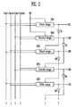
- FIG. 2 is a schematic view showing the emission driver of FIG. 1 .
- an emission driver 30 of the present invention includes stages 321 , 322 , . . . coupled to respective light emitting control signals E 1 to En.
- the respective stages 321 , 322 , . . . are driven by two clock signals.
- Timing controller 60 supplies four clock signals Clk 1 , Clk 1 b , Clk 2 , and Clk 2 b and starting signals SP to the emission driver 30 .
- the first clock signal Clk 1 and the inverted first clock signal Clk 1 b are supplied to odd stages 321 , 323 , 325 . . .
- the second clock signal Clk 2 and the inverted second clock signal Clk 2 b are supplied to even stages 322 , 324 , . . . .
- the starting signals SP are supplied to the first stage 321 and the second stage 322 .
- the first clock signal Clk 1 and the second clock signal Clk 2 have the same period and are supplied to be overlapped by 1 ⁇ 4 periods at their high levels (or low levels).
- An output of an i th (i is a natural number) stage 32 i is supplied to an i+2 nd stage 32 i+ 2 via an inverter IN.
- the output of a first stage 321 is supplied to the third stage 323 via the inverter IN
- the output of the third stage 323 is supplied to the fifth stage 325 via the inverter IN.
- the odd stages 323 , 325 , . . . are supplied with the output of odd stages.
- the output of the second stage 322 is supplied to the fourth stage 324 via the inverter IN
- the output of the fourth stage 324 is supplied to the sixth stage via the inverter IN. Accordingly, the even stages 324 , . . . are supplied with the output of even stages.
- FIG. 4 illustrates an embodiment of a circuit for the respective stages.
- a first stage 321 coupled to a first clock signal Clk 1 and an inverted first clock signal Clk 1 b will be described in FIG. 4 .
- a first stage 321 includes an input unit 34 that supplies any of a first signal and a second signal according to clock signals Clk 1 and Clk 1 b and stating signals SP, an output unit 36 that controls whether light emitting control signals are generated or not according to the first signal or the second signal supplied from the input unit 34 , and an initial driving controller 38 that controls the light emitting signals to be suppliable during an initial driving period.
- the input unit 34 includes a first transistor M 1 coupled to a third power supply VDD and a first input terminal, a third transistor M 3 coupled to the first input terminal and a second input terminal, a second transistor M 2 coupled to the third transistor M 3 and a third input terminal, and a first capacitor C 1 coupled between a gate electrode of the second transistor M 2 and a first electrode (source electrode) thereof.
- a first electrode of the first transistor M 1 is coupled to the third power supply VDD and a gate electrode thereof is coupled to the first input terminal.
- the first input terminal is a terminal supplied with the first clock signal clk 1 .
- a second electrode (drain electrode) of the first transistor M 1 is coupled to a first node N 1 .
- the first transistor M 1 is turned on when the first clock signal Clk 1 is at a low level, to supply voltage of the third power supply VDD to the first node N 1 .
- a first electrode of the second transistor M 2 is coupled to the first node N 1 , and a second electrode thereof is coupled to the third input terminal.
- the third input terminal is supplied with the inverted first clock signal clk 1 b .
- a gate electrode of the second transistor M 2 is coupled to a first electrode of the third transistor M 3 .
- the second transistor M 2 is turned on or turned off according to the voltage charged in the first capacitor C 1 .
- the first electrode of the third transistor M 3 is coupled to the gate electrode of the second transistor M 2 , and a second electrode thereof is coupled to the second input terminal.
- the second input terminal is supplied with the starting signals SP or light emitting control signals inverted from a previous stage.
- a gate electrode of the third transistor M 3 is coupled to the first input terminal.
- the third transistor M 3 is turned on when the first clock signal Clk 1 is at a low level.
- the first capacitor C 1 is coupled to the gate electrode of the second transistor M 2 and the first electrode thereof.
- the first capacitor C 1 is charged with voltage, which can turn on the second transistor M 2 when the third transistor M 3 is turned on and the starting signals SP are supplied to the second input terminal. It is not charged with voltage otherwise.
- the output unit 36 outputs the light emitting signals (high level) in the case where the second signals (low level) are supplied to the first node N 1 , and it does not output the light emitting signals in other case (that is, when the first signal (high level) is supplied to the first node N 1 ).
- the output unit 36 includes a fourth transistor M 4 coupled to the third power supply VDD, a sixth transistor M 6 , an eighth transistor M 8 , a fifth transistor M 5 coupled to a fourth power supply VSS, a seventh transistor M 7 , a ninth transistor M 9 , and a second capacitor C 2 coupled between a gate electrode of the ninth transistor M 9 and a first electrode thereof.
- a first electrode of the fourth transistor M 4 is coupled to the third power supply VDD, and a second electrode thereof is coupled to the second node N 2 .
- a gate electrode of the fourth transistor M 4 is coupled to the first node N 1 .
- a first electrode of the fifth transistor M 5 is coupled to the second node N 2 , and a second electrode thereof is coupled to the fourth power supply VSS.
- a gate electrode of the fifth transistor M 5 is coupled to the first input terminal.
- a first electrode of the sixth transistor M 6 is coupled to the third power supply VDD, and a second electrode thereof is coupled to a first electrode of the seventh transistor M 7 .
- a gate electrode of the sixth transistor M 6 is coupled to the second node N 2 .
- the first electrode of the seventh transistor M 7 is coupled to the second electrode of the sixth transistor M 6 , and a second electrode thereof is coupled to the fourth power supply VSS.
- a gate electrode of the seventh transistor M 7 is coupled to the first node N 1 .
- a first electrode of the eighth transistor M 8 is coupled to the third power supply VDD, and a second electrode thereof is coupled to the light emitting control line E 1 .
- a gate electrode of the eighth transistor M 8 is coupled to the second electrode of the sixth transistor M 6 .
- a first electrode of the ninth transistor M 9 is coupled to the light emitting control line E 1 , and a second electrode thereof is coupled to the fourth power supply VSS.
- the gate electrode of the ninth transistor M 9 is coupled to the second node N 2 .
- the second capacitor C 2 is coupled between the gate electrode of the ninth transistor M 9 and the first electrode thereof.
- the second capacitor C 2 controls a turn-on and a turn-off of the ninth transistor M 9 .
- the initial driving controller 38 controls the light emitting control signals to be supplied to the light emitting control line E 1 during an initial driving period.
- the initial driving controller 38 is driven during the initial driving period and not driven during a normal driving period that the pixels 50 are driven.
- the initial driving controller 38 includes a tenth transistor M 10 and an eleventh transistor M 11 .
- a first electrode of the tenth transistor M 10 is coupled to the third power supply VDD, and a second electrode thereof is coupled to the gate electrode of the second transistor M 2 .
- a gate electrode of the tenth transistor M 10 is coupled to a fourth input terminal input with initial control signals RS (active low level signal).
- the a tenth transistor M 10 is turned on when the initial control signals RS are supplied, and is turned off when the initial control signals RS are not supplied.
- the input unit 34 , the output unit 36 , and the initial driving controller 38 use only the same type of transistors, pMOS transistors. In other embodiments other transistors may be used, or multiple types may be used.
- a first electrode of the eleventh transistor M 1 is coupled to the first node N 1 , and a second electrode thereof is coupled to the fourth power supply VSS.
- a gate electrode of the eleventh transistor M 1 is coupled to the fourth input terminal.
- the eleventh transistor M 11 is turned on when the initial control signals are supplied, and is turned off when the initial control signals are not supplied.
- FIG. 3 is a waveform view showing a normal driving process of a stage during a normal driving period. During the normal driving period, the tenth transistor M 10 and the eleventh transistor M 11 maintain in a turn-off state.
- first a clock signal Clk 1 is set as a low level and an inverted first clock signal Clkb 1 is set as a high level during a first period T 1 .
- a first transistor M 1 and a third transistor M 3 are turned on by the first clock signal Clk 1 .
- the first transistor M 1 Because the first transistor M 1 is on, the voltage of a first node N 1 rises to the voltage of a third power supply VDD. Accordingly, the voltage of a first signal (high level) is applied to the first node N 1 . Because the third transistor M 3 is turned on, the gate electrode voltage of the second transistor M 2 falls to a low level because of the starting signal SP supplied during the first period T 1 . In this case, the first capacitor C 1 is charged with a voltage of a difference between the voltage of the third power supply VDD applied to the first node N 1 and the low level voltage applied to a gate electrode of a second transistor M 2 .
- a voltage level of the inverted first clock signal Clk 1 b is set as a high level.
- the high level voltage of the inverted first clock signal Clk 1 b may be set to be the same as the voltage of the third power supply VDD. Then, even when the first transistor M 1 and the second transistor M 2 are simultaneously turned on, the voltage of the first node N 1 can be stably maintained at the same high level.
- a fourth transistor M 4 and a seventh transistor M 7 are turned off.
- the first clock signal Clk 1 maintains a low level
- a fifth transistor M 5 maintains a turn-off state because of the voltage stored in a second capacitor C 2 .
- the second capacitor C 2 is charged with voltage of more than VDD ⁇ (VSS+
- the sixth transistor M 6 is turned on by voltage applied to a second node N 2 (that is, voltage because of the second capacitor C 2 ), as shown in FIG. 5 b .
- the voltage of the third power supply VDD is supplied to the gate electrode of the eighth transistor M 8 . Accordingly, the eighth transistor M 8 is off.
- the ninth transistor M 9 maintains a turn-on state because of the voltage charged in the second capacitor C 2 and accordingly, the light emitting control line E maintains output voltage of a fourth power supply VSS.
- the second capacitor C 2 is charged with voltage of more than VDD ⁇ (VSS+
- the first clock signal Clk 1 is set as a high level and the inverted clock signal Clk 1 b is set as a low level.
- the first clock signal Clk 1 is set as a high level
- the first transistor M 1 , the third transistor M 3 , and the fifth transistor M 5 are turned off, as shown in FIG. 5 c .
- the second transistor M 2 is still on because of the voltage charged in the first capacitor C 1 during a previous period. Because the second transistor M 2 is on, the voltage of the first node N 1 falls to a level of the inverted first clock signal Clk 1 b (for example, the fourth power supply VSS), that is, a low level.
- the fourth transistor M 4 and the seventh transistor M 7 are turned on. Because the fourth transistor M 4 is turned on, the voltage of the second node N 2 rises to the voltage of the third power supply VDD. As a result, the sixth transistor M 6 and the ninth transistor M 9 are turned off. Because the seventh transistor M 7 is on, the voltage of the gate electrode of the eighth transistor M 8 falls to the voltage of the fourth power supply VSS so that the eighth transistor M 8 is turned on. Because the eighth transistor M 8 is on, the voltage of the third power supply VDD is supplied to the light emitting control line E 1 .
- the light emitting control signals are supplied to the light emitting control line E 1 .
- the voltage of the third power supply VDD is supplied across the second capacitor C 2 so that the second capacitor C 2 is not charged with voltage.
- the first clock signal Clk 1 is set as a low level, and the inverted first clock signal Clk 1 b is set as a high level.
- the first transistor M 1 , the third transistor M 3 , and the fifth transistor M 5 are turned on by the first clock signal Clk 1 , as shown in FIG. 5 d . Because the first transistor M 1 is turned on, the voltage of the first node N 1 rises to the voltage of the third power supply VDD. In other words, the voltage of the first signal (high level) is-applied to the first node N 1 .
- the third transistor M 3 is turned on, and the starting signals SP maintains voltage at high level (for example, the voltage of the third power supply VDD), the second transistor M 2 is off.
- the voltage at both terminals of the first capacitor C 1 are the voltage of the third power supply VDD so that the first capacitor C 1 is not charged.
- the first capacitor C 1 is charged with a predetermined voltage only in the period where the starting signals SP are set as a low level, and is not charged with voltage otherwise.
- the second transistor M 2 is turned off, the voltage of the first signal is applied to the first node N 1 , and the inverted first clock signal Clk 1 b maintains a high level. Therefore, although the first node N 1 maintains the voltage of the first signal, current is prevented from flowing via the second transistor M 2 and power consumption is therefore reduced.
- the fifth transistor M 5 When the fifth transistor M 5 is on, the voltage of the second node N 2 is pulled down to voltage of VSS+
- the fourth transistor M 4 and the seventh transistor M 7 are turned off by the voltage of the first signal applied to the first node N 1 , and the sixth transistor M 6 and the ninth transistor M 9 are turned on by the voltage charged in the second capacitor C 2 .
- the sixth transistor Because the sixth transistor is turned on, the voltage of the third power supply VDD is applied to the gate electrode of the eighth transistor M 8 so that the eighth transistor M 8 is turned off. Because the ninth transistor M 9 is on, the voltage of the light emitting control line D 1 , maintaining a high state during the second period T 2 , falls to the voltage of the fourth power supply VSS. At this time, the fifth transistor is set as a turn-off state (accordingly, N 2 is in a floating state) so that the voltage charged in the second capacitor C 2 is maintained and accordingly, the voltage of the light emitting control line E 1 is pulled down to the voltage of the fourth power supply VSS.
- the voltage of only the first signal (high level) is applied to the first node N 1 before the starting signals SP are supplied again.
- the first capacitor C 1 is not charged with voltage before the starting signals SP are supplied again, and accordingly the second transistor M 2 maintains a turn-off state.
- the ninth transistor M 9 supplies the voltage of the fourth power supply VSS to the light emitting control line E 1 during the remainder of the frame period, because of the voltage charged in the second capacitor C 2 .
- FIG. 6 illustrates an initial control signal supplied during an initial driving period.
- an initial control signal RS (low level) is supplied during an initial driving period and the initial control signal RS is not supplied during a normal driving period.
- the tenth transistor M 10 and the eleventh transistor M 11 are turned on, as shown in FIG. 7 . Because the tenth transistor M 10 is on, the voltage of a third power supply VDD is supplied to the gate electrode of the second transistor M 2 and accordingly, the second transistor M 2 is turned off.
- the eleventh transistor M 11 is on, the voltage of the fourth power supply VSS is supplied to the first node N 1 . In other words, a second signal is supplied to the first node N 1 . Because the second signal is supplied to the first node N 1 , the fourth transistor M 4 and the seventh transistor M 7 are turned on.
- the fourth transistor M 4 is turned on, the voltage of the third power supply VDD is supplied to a second node N 2 so that a sixth transistor M 6 is turned off. Because the seventh transistor M 7 is turned on, the voltage of the fourth power supply VSS is supplied to the gate electrode of the eighth transistor M 8 so that the eighth transistor M 8 is turned on. Because the eight transistor M 8 is turned on, the voltage of the third power supply VDD is supplied to the light emitting control line E 1 .
- the initial driving controller 38 is controlled to supply the light emitting control signals to the all light emitting control lines E 1 to En. Then, light emitting of the pixels 50 during the initial driving period can be prevented, making it possible to improve display quality.
Landscapes
- Engineering & Computer Science (AREA)
- Physics & Mathematics (AREA)
- Computer Hardware Design (AREA)
- General Physics & Mathematics (AREA)
- Theoretical Computer Science (AREA)
- Microelectronics & Electronic Packaging (AREA)
- Power Engineering (AREA)
- Control Of Indicators Other Than Cathode Ray Tubes (AREA)
- Electroluminescent Light Sources (AREA)
- Control Of El Displays (AREA)
Abstract
Description
Claims (20)
Applications Claiming Priority (2)
| Application Number | Priority Date | Filing Date | Title |
|---|---|---|---|
| KR1020080020021A KR100911982B1 (en) | 2008-03-04 | 2008-03-04 | Emission driver and organic light emitting display device using same |
| KR10-2008-0020021 | 2008-03-04 |
Publications (2)
| Publication Number | Publication Date |
|---|---|
| US20090225068A1 US20090225068A1 (en) | 2009-09-10 |
| US8339424B2 true US8339424B2 (en) | 2012-12-25 |
Family
ID=40483881
Family Applications (1)
| Application Number | Title | Priority Date | Filing Date |
|---|---|---|---|
| US12/380,464 Active 2030-08-24 US8339424B2 (en) | 2008-03-04 | 2009-02-27 | Emission driver and organic light emitting display using the same |
Country Status (5)
| Country | Link |
|---|---|
| US (1) | US8339424B2 (en) |
| EP (1) | EP2099018B1 (en) |
| JP (1) | JP4887334B2 (en) |
| KR (1) | KR100911982B1 (en) |
| CN (1) | CN101527110B (en) |
Cited By (9)
| Publication number | Priority date | Publication date | Assignee | Title |
|---|---|---|---|---|
| US20130135284A1 (en) * | 2011-11-30 | 2013-05-30 | Au Optronics Corporation | Display panel and gate driver therein |
| US20180096732A1 (en) * | 2016-10-04 | 2018-04-05 | Int Tech Co., Ltd. | High stability shift register with adjustable pulse width |
| US10043432B2 (en) * | 2015-07-02 | 2018-08-07 | Samsung Display Co., Ltd. | Emission driver and display device including the same |
| US20190066604A1 (en) * | 2017-08-31 | 2019-02-28 | Lg Display Co., Ltd. | Gate driving circuit and electroluminescent display using the same |
| US10614732B2 (en) | 2017-02-20 | 2020-04-07 | Samsung Display Co., Ltd. | Stage circuit and scan driver using the same |
| USRE48358E1 (en) | 2012-08-21 | 2020-12-15 | Samsung Display Co., Ltd. | Emission control driver and organic light emitting display device having the same |
| US10937369B2 (en) | 2018-11-12 | 2021-03-02 | Samsung Display Co., Ltd. | Stage and emission control driver having the same |
| US11100856B2 (en) * | 2016-06-17 | 2021-08-24 | Samsung Display Co., Ltd. | Stage and organic light emitting display device using the same |
| US11727885B2 (en) | 2021-12-09 | 2023-08-15 | Samsung Display Co., Ltd. | Scan driver and display device including the same |
Families Citing this family (34)
| Publication number | Priority date | Publication date | Assignee | Title |
|---|---|---|---|---|
| KR101581401B1 (en) * | 2009-11-06 | 2015-12-31 | 삼성디스플레이 주식회사 | Scan drive |
| US8054935B2 (en) | 2009-11-13 | 2011-11-08 | Au Optronics Corporation | Shift register with low power consumption |
| KR101790705B1 (en) * | 2010-08-25 | 2017-10-27 | 삼성디스플레이 주식회사 | Bi-directional scan driver and display device using the same |
| KR101479297B1 (en) * | 2010-09-14 | 2015-01-05 | 삼성디스플레이 주식회사 | Scan driver and organic light emitting display using the same |
| KR101719187B1 (en) * | 2010-09-14 | 2017-03-24 | 삼성디스플레이 주식회사 | Emission driver and organic light emitting display using the same |
| KR101735804B1 (en) * | 2010-12-13 | 2017-05-16 | 삼성디스플레이 주식회사 | Stereopsis display device and driving method thereof |
| KR101748743B1 (en) | 2010-12-27 | 2017-06-20 | 삼성디스플레이 주식회사 | Pixel and Organic Light Emitting Display Device Using the same |
| KR101986708B1 (en) * | 2011-01-05 | 2019-06-11 | 삼성디스플레이 주식회사 | Organic Light Emitting Display Device |
| KR101944465B1 (en) * | 2011-01-06 | 2019-02-07 | 삼성디스플레이 주식회사 | Emission Driver and Organic Light Emitting Display Device Using the same |
| KR101871188B1 (en) * | 2011-02-17 | 2018-06-28 | 삼성디스플레이 주식회사 | Organic Light Emitting Display and Driving Method Thereof |
| KR20130000020A (en) * | 2011-06-22 | 2013-01-02 | 삼성디스플레이 주식회사 | Stage circuit and emission driver using the same |
| KR101972018B1 (en) | 2012-11-14 | 2019-04-25 | 삼성디스플레이 주식회사 | Display device and emitting driver for the same |
| CN103268749B (en) * | 2012-11-21 | 2015-04-15 | 上海天马微电子有限公司 | Inverter, AMOLED compensation circuit and display panel |
| CN103000151B (en) * | 2012-11-29 | 2014-09-10 | 京东方科技集团股份有限公司 | Gate drive device and display device |
| KR102050581B1 (en) * | 2013-06-21 | 2019-12-02 | 삼성디스플레이 주식회사 | Stage Circuit and Organic Light Emitting Display Device Using the same |
| KR102238640B1 (en) * | 2014-11-10 | 2021-04-12 | 엘지디스플레이 주식회사 | Organic Light Emitting diode Display |
| KR102299155B1 (en) * | 2014-12-09 | 2021-09-08 | 엘지디스플레이 주식회사 | Organic Light Emitting Diode |
| WO2016154909A1 (en) * | 2015-03-31 | 2016-10-06 | 上海和辉光电有限公司 | Transmitting control line driver, oled panel having same, and display device |
| KR102425574B1 (en) * | 2015-06-29 | 2022-07-27 | 삼성디스플레이 주식회사 | Emission driver and organic light emitting display device having the same |
| KR102431435B1 (en) * | 2015-10-26 | 2022-08-12 | 삼성디스플레이 주식회사 | Emissioin driver and display device including the same |
| KR102613407B1 (en) * | 2015-12-31 | 2023-12-13 | 엘지디스플레이 주식회사 | display apparatus, gate driving circuit and driving method thereof |
| KR102566782B1 (en) * | 2016-03-09 | 2023-08-16 | 삼성디스플레이 주식회사 | Scan driver and display apparatus having the same |
| CN106448580A (en) * | 2016-05-25 | 2017-02-22 | 深圳市华星光电技术有限公司 | Level shift circuit and display panel having level shift circuit |
| CN108806588B (en) * | 2017-04-28 | 2020-06-12 | 昆山国显光电有限公司 | Light-emitting control circuit, light-emitting control method and shift register |
| KR102511046B1 (en) * | 2017-11-20 | 2023-03-16 | 엘지디스플레이 주식회사 | Gate driver and electroluminescence display device using the same |
| KR102585515B1 (en) * | 2018-07-19 | 2023-10-05 | 엘지디스플레이 주식회사 | Organic light emitting display apparatus |
| WO2020206593A1 (en) * | 2019-04-08 | 2020-10-15 | 深圳市柔宇科技有限公司 | Display panel and display device |
| KR102098331B1 (en) * | 2019-04-29 | 2020-04-08 | 삼성디스플레이 주식회사 | Emission driver and organic light emitting display deivce including the same |
| CN110619852B (en) * | 2019-09-26 | 2020-11-13 | 昆山工研院新型平板显示技术中心有限公司 | Scanning circuit, display panel and display device |
| US11005475B1 (en) * | 2020-01-06 | 2021-05-11 | Innolux Corporation | Emission driver and pump unit |
| KR102186759B1 (en) * | 2020-04-01 | 2020-12-07 | 삼성디스플레이 주식회사 | Emission driver and organic light emitting display deivce including the same |
| KR102763628B1 (en) * | 2020-05-22 | 2025-02-10 | 삼성디스플레이 주식회사 | Emission driver, display apparatus including the same, method of driving display apparatus |
| CN111627372B (en) * | 2020-06-30 | 2022-07-26 | 武汉天马微电子有限公司 | Shift register and circuit thereof, display panel and electronic equipment |
| KR20240100591A (en) * | 2022-12-22 | 2024-07-02 | 삼성디스플레이 주식회사 | Shift register and display apparatus having the same |
Citations (15)
| Publication number | Priority date | Publication date | Assignee | Title |
|---|---|---|---|---|
| US5454018A (en) | 1993-12-30 | 1995-09-26 | Sgs-Thomson Microelectronics, Inc. | Counter circuit with automatic reset |
| KR20040078437A (en) | 2003-03-04 | 2004-09-10 | 엘지전자 주식회사 | Method and apparatus for driving active matrix type electro-luminescence display device |
| KR20050085414A (en) | 2002-12-05 | 2005-08-29 | 파브리스틸 프로덕트 인코포레이티드 | Self-threading female fastener elements and method of forming same |
| US20060044230A1 (en) * | 2004-08-30 | 2006-03-02 | Ki-Myeong Eom | Signal driving method and apparatus for a light emitting display |
| KR20060031547A (en) | 2004-10-08 | 2006-04-12 | 삼성에스디아이 주식회사 | Pixel and light emitting display device and driving method thereof |
| JP2006243174A (en) | 2005-03-01 | 2006-09-14 | Sony Corp | Power-on method |
| JP2006243175A (en) | 2005-03-01 | 2006-09-14 | Sony Corp | Power-on method |
| KR100646992B1 (en) | 2005-09-13 | 2006-11-23 | 삼성에스디아이 주식회사 | Light emission control line driver and organic light emitting display device using the same |
| WO2007013010A2 (en) | 2005-07-26 | 2007-02-01 | Koninklijke Philips Electronics N.V. | A multiple input circuit |
| JP2007035188A (en) | 2005-07-28 | 2007-02-08 | Toshiba Matsushita Display Technology Co Ltd | Shift register and flat display device |
| KR20070019463A (en) | 2005-08-12 | 2007-02-15 | 삼성에스디아이 주식회사 | Organic electroluminescent display |
| US20070046608A1 (en) | 2005-08-26 | 2007-03-01 | Bo-Yong Chung | Emission driving device of organic light emitting display device |
| US20070057877A1 (en) | 2005-09-15 | 2007-03-15 | Sang-Moo Choi | Organic light emitting display device and method of operating the same |
| JP2007114476A (en) | 2005-10-20 | 2007-05-10 | Toshiba Matsushita Display Technology Co Ltd | Driving method of active matrix display device |
| KR20070100545A (en) | 2006-04-07 | 2007-10-11 | 엘지.필립스 엘시디 주식회사 | Organic light emitting diode display device and driving method thereof |
Family Cites Families (1)
| Publication number | Priority date | Publication date | Assignee | Title |
|---|---|---|---|---|
| KR101240645B1 (en) * | 2005-08-29 | 2013-03-08 | 삼성디스플레이 주식회사 | Display device and driving method thereof |
-
2008
- 2008-03-04 KR KR1020080020021A patent/KR100911982B1/en active Active
- 2008-06-13 JP JP2008155153A patent/JP4887334B2/en active Active
-
2009
- 2009-02-27 US US12/380,464 patent/US8339424B2/en active Active
- 2009-03-03 CN CN2009100080791A patent/CN101527110B/en active Active
- 2009-03-04 EP EP09154276A patent/EP2099018B1/en active Active
Patent Citations (16)
| Publication number | Priority date | Publication date | Assignee | Title |
|---|---|---|---|---|
| US5454018A (en) | 1993-12-30 | 1995-09-26 | Sgs-Thomson Microelectronics, Inc. | Counter circuit with automatic reset |
| KR20050085414A (en) | 2002-12-05 | 2005-08-29 | 파브리스틸 프로덕트 인코포레이티드 | Self-threading female fastener elements and method of forming same |
| KR20040078437A (en) | 2003-03-04 | 2004-09-10 | 엘지전자 주식회사 | Method and apparatus for driving active matrix type electro-luminescence display device |
| US20060044230A1 (en) * | 2004-08-30 | 2006-03-02 | Ki-Myeong Eom | Signal driving method and apparatus for a light emitting display |
| KR20060031547A (en) | 2004-10-08 | 2006-04-12 | 삼성에스디아이 주식회사 | Pixel and light emitting display device and driving method thereof |
| JP2006243174A (en) | 2005-03-01 | 2006-09-14 | Sony Corp | Power-on method |
| JP2006243175A (en) | 2005-03-01 | 2006-09-14 | Sony Corp | Power-on method |
| WO2007013010A2 (en) | 2005-07-26 | 2007-02-01 | Koninklijke Philips Electronics N.V. | A multiple input circuit |
| JP2007035188A (en) | 2005-07-28 | 2007-02-08 | Toshiba Matsushita Display Technology Co Ltd | Shift register and flat display device |
| KR20070019463A (en) | 2005-08-12 | 2007-02-15 | 삼성에스디아이 주식회사 | Organic electroluminescent display |
| US20070046608A1 (en) | 2005-08-26 | 2007-03-01 | Bo-Yong Chung | Emission driving device of organic light emitting display device |
| KR100646992B1 (en) | 2005-09-13 | 2006-11-23 | 삼성에스디아이 주식회사 | Light emission control line driver and organic light emitting display device using the same |
| EP1763003A2 (en) | 2005-09-13 | 2007-03-14 | Samsung SDI Co., Ltd. | Emission control line driver and organic light emitting display using the emission control line driver |
| US20070057877A1 (en) | 2005-09-15 | 2007-03-15 | Sang-Moo Choi | Organic light emitting display device and method of operating the same |
| JP2007114476A (en) | 2005-10-20 | 2007-05-10 | Toshiba Matsushita Display Technology Co Ltd | Driving method of active matrix display device |
| KR20070100545A (en) | 2006-04-07 | 2007-10-11 | 엘지.필립스 엘시디 주식회사 | Organic light emitting diode display device and driving method thereof |
Non-Patent Citations (2)
| Title |
|---|
| Certificate of Patent for Invention dated Jun. 15, 2011 for Chinese Patent No. ZL200910008079.1 which shares priority of Korean Patent Application No. KR 10-2008-0020021 with captioned U.S. Appl. No. 12/380,464. |
| European Search Report for corresponding European Patent Application No. 09154276.1 dated May 4, 2009. |
Cited By (14)
| Publication number | Priority date | Publication date | Assignee | Title |
|---|---|---|---|---|
| US8860651B2 (en) * | 2011-11-30 | 2014-10-14 | Au Optronics Corporation | Display panel and gate driver therein |
| US20130135284A1 (en) * | 2011-11-30 | 2013-05-30 | Au Optronics Corporation | Display panel and gate driver therein |
| USRE48358E1 (en) | 2012-08-21 | 2020-12-15 | Samsung Display Co., Ltd. | Emission control driver and organic light emitting display device having the same |
| US10043432B2 (en) * | 2015-07-02 | 2018-08-07 | Samsung Display Co., Ltd. | Emission driver and display device including the same |
| US11100856B2 (en) * | 2016-06-17 | 2021-08-24 | Samsung Display Co., Ltd. | Stage and organic light emitting display device using the same |
| US12315439B2 (en) | 2016-06-17 | 2025-05-27 | Samsung Display Co., Ltd. | Stage and organic light emitting display device using the same |
| US11640788B2 (en) | 2016-06-17 | 2023-05-02 | Samsung Display Co., Ltd. | Stage and organic light emitting display device using the same |
| US20180096732A1 (en) * | 2016-10-04 | 2018-04-05 | Int Tech Co., Ltd. | High stability shift register with adjustable pulse width |
| US10600492B2 (en) * | 2016-10-04 | 2020-03-24 | Int Tech Co., Ltd. | High stability shift register with adjustable pulse width |
| US10614732B2 (en) | 2017-02-20 | 2020-04-07 | Samsung Display Co., Ltd. | Stage circuit and scan driver using the same |
| US10762853B2 (en) * | 2017-08-31 | 2020-09-01 | Lg Display Co., Ltd. | Gate driving circuit and electroluminescent display using the same |
| US20190066604A1 (en) * | 2017-08-31 | 2019-02-28 | Lg Display Co., Ltd. | Gate driving circuit and electroluminescent display using the same |
| US10937369B2 (en) | 2018-11-12 | 2021-03-02 | Samsung Display Co., Ltd. | Stage and emission control driver having the same |
| US11727885B2 (en) | 2021-12-09 | 2023-08-15 | Samsung Display Co., Ltd. | Scan driver and display device including the same |
Also Published As
| Publication number | Publication date |
|---|---|
| EP2099018A1 (en) | 2009-09-09 |
| JP2009211028A (en) | 2009-09-17 |
| EP2099018B1 (en) | 2012-02-22 |
| KR100911982B1 (en) | 2009-08-13 |
| CN101527110B (en) | 2011-06-15 |
| JP4887334B2 (en) | 2012-02-29 |
| CN101527110A (en) | 2009-09-09 |
| US20090225068A1 (en) | 2009-09-10 |
Similar Documents
| Publication | Publication Date | Title |
|---|---|---|
| US8339424B2 (en) | Emission driver and organic light emitting display using the same | |
| US8299982B2 (en) | Emission control line driver and organic light emitting display using the emission control line driver | |
| CN1312651C (en) | Luminous display, driving method and its picture element circuit and display device | |
| US8665182B2 (en) | Emission control driver and organic light emitting display device using the same | |
| EP2128848A1 (en) | Pixel and organic light emiting display using the same | |
| US8717257B2 (en) | Scan driver and organic light emitting display using the same | |
| US8937489B2 (en) | Inverter and scan driver using the same | |
| US20060151745A1 (en) | Organic light emitting display and driving method thereof | |
| US8970458B2 (en) | Organic light emitting display and method of driving the same | |
| US9384692B2 (en) | Organic light emitting display having a reduced number of signal lines | |
| US8400377B2 (en) | Pixel and organic light emitting display device using the same | |
| US9549450B2 (en) | Pixel and organic light emitting display device using the same | |
| US8743024B2 (en) | Emission control driver and organic light emitting display using the same | |
| US8432342B2 (en) | Pixel and organic light emitting display using the same | |
| US20080055304A1 (en) | Organic light emitting display and driving method thereof | |
| US8314788B2 (en) | Organic light emitting display device | |
| US8723765B2 (en) | Stage circuit and scan driver using the same | |
| US9269296B2 (en) | Pixel and organic light emitting display device using the same | |
| US20110227908A1 (en) | Organic light emitting display | |
| CN116863874B (en) | Scan driving circuit, scan driving method and display device | |
| CN105448235A (en) | AMOLED (Active Matrix/Organic Light Emitting Diode) pixel unit and driving method thereof, and AMOLED display device | |
| KR100836431B1 (en) | Pixel and organic light emitting display device using same | |
| KR100821040B1 (en) | Organic light emitting display |
Legal Events
| Date | Code | Title | Description |
|---|---|---|---|
| AS | Assignment |
Owner name: SAMSUNG MOBILE DISPLAY CO., LTD., KOREA, REPUBLIC Free format text: ASSIGNMENT OF ASSIGNORS INTEREST;ASSIGNORS:JEONG, SEON-I;KIM, MI-HAE;EOM, KI-MYEONG;AND OTHERS;REEL/FRAME:022396/0894 Effective date: 20090223 |
|
| FEPP | Fee payment procedure |
Free format text: PAYOR NUMBER ASSIGNED (ORIGINAL EVENT CODE: ASPN); ENTITY STATUS OF PATENT OWNER: LARGE ENTITY |
|
| AS | Assignment |
Owner name: SAMSUNG DISPLAY CO., LTD., KOREA, REPUBLIC OF Free format text: MERGER;ASSIGNOR:SAMSUNG MOBILE DISPLAY CO., LTD.;REEL/FRAME:028921/0334 Effective date: 20120702 |
|
| FEPP | Fee payment procedure |
Free format text: PAYER NUMBER DE-ASSIGNED (ORIGINAL EVENT CODE: RMPN); ENTITY STATUS OF PATENT OWNER: LARGE ENTITY Free format text: PAYOR NUMBER ASSIGNED (ORIGINAL EVENT CODE: ASPN); ENTITY STATUS OF PATENT OWNER: LARGE ENTITY |
|
| STCF | Information on status: patent grant |
Free format text: PATENTED CASE |
|
| FPAY | Fee payment |
Year of fee payment: 4 |
|
| MAFP | Maintenance fee payment |
Free format text: PAYMENT OF MAINTENANCE FEE, 8TH YEAR, LARGE ENTITY (ORIGINAL EVENT CODE: M1552); ENTITY STATUS OF PATENT OWNER: LARGE ENTITY Year of fee payment: 8 |
|
| MAFP | Maintenance fee payment |
Free format text: PAYMENT OF MAINTENANCE FEE, 12TH YEAR, LARGE ENTITY (ORIGINAL EVENT CODE: M1553); ENTITY STATUS OF PATENT OWNER: LARGE ENTITY Year of fee payment: 12 |