US8330637B2 - Time-to-digital converter and operation method thereof - Google Patents
Time-to-digital converter and operation method thereof Download PDFInfo
- Publication number
- US8330637B2 US8330637B2 US13/089,558 US201113089558A US8330637B2 US 8330637 B2 US8330637 B2 US 8330637B2 US 201113089558 A US201113089558 A US 201113089558A US 8330637 B2 US8330637 B2 US 8330637B2
- Authority
- US
- United States
- Prior art keywords
- phase
- tdc
- input signal
- delay
- signals
- Prior art date
- Legal status (The legal status is an assumption and is not a legal conclusion. Google has not performed a legal analysis and makes no representation as to the accuracy of the status listed.)
- Active, expires
Links
Images


Classifications
-
- G—PHYSICS
- G04—HOROLOGY
- G04F—TIME-INTERVAL MEASURING
- G04F10/00—Apparatus for measuring unknown time intervals by electric means
- G04F10/005—Time-to-digital converters [TDC]
Definitions
- the present invention relates to a Time-to-Digital Converter (TDC) and an operation method thereof. More particularly, the present invention relates to a TDC having a high resolution at a Radio Frequency (RF) input frequency by using a Phase-Interpolation (PI) technique and a Time Amplifier (TA), and an operation method thereof.
- TDC Time-to-Digital Converter
- PI Phase-Interpolation
- TA Time Amplifier
- a wireless communication transceiver and the like include a phase-locked loop to provide a Local Oscillator (LO) frequency.
- an analog phase-locked loop is used, which may cause a reduction in process scale.
- the analog phase-locked loop may be digitally constructed. In this case, however, the analog phase-locked loop may be insensitive to process variations.
- a digital phase-locked loop is used.
- a Time-to-Digital Converter (TDC) is used to detect a phase difference between an output frequency of a digital oscillator and a reference frequency, and the performance of the digital phase looked loop depends on a resolution of the TDC.
- TDC Time-to-Digital Converter
- the TDC receives two input signals, and delays one of the input signals through a delay line step by step.
- the TDC compares a waveform of the input signal delayed step by step with a waveform of the other input signal in terms of the rising edge, and outputs the comparison results in a digital code.
- a phase difference between the two input signals may be identified based on the output digital code.
- FIG. 1 schematically illustrates a TDC with a single delay line according to the related art.
- a TDC 100 includes two input signal lines, L inverters 106 - 1 ⁇ 106 -L for signal delay, and (L+1) comparators 108 - 0 ⁇ 108 -L, which are implemented with their associated flip-flops.
- the TDC 100 receives two input signals: a Digital Controlled Oscillator (DCO) frequency F DCO 102 and a reference frequency F REF 104 .
- the F DCO 102 is delayed by each of the L inverters 106 - 1 ⁇ 106 -L and then input to each of the (L+1) comparators 108 - 0 ⁇ 108 -L.
- Each of the (L+1) comparators 108 - 0 ⁇ 108 -L compares a rising edge of the F DCO delayed by each of the inverters 106 - 1 ⁇ 106 -L with a rising edge of the F REF 104 , and outputs the comparison results in a digital code.
- a phase difference between the input signals may be identified based on the output digital code.
- a resolution of the TDC 100 is determined by a delay time of the inverters 106 - 1 ⁇ 106 -L. Since a delay time of an inverter is determined by a size of a transistor constituting the inverter, a resolution of the TDC may be limited to a specific value in a specific process.
- RF Radio Frequency
- PI Phase-Interpolation
- TA Time Amplifier
- an aspect of the present invention is to provide a Time-to-Digital Converter (TDC) using a Phase-Interpolation (PI) technique and a Time Amplifier (TA), and an operation method thereof.
- TDC Time-to-Digital Converter
- PI Phase-Interpolation
- TA Time Amplifier
- Another aspect of the present invention is to provide a TDC using a PI technique that uses a resistor auto-tuning scheme, and a TA that increases its gain with a time difference caused by the use of additional inverters, and an operation method thereof.
- Another aspect of the present invention is to provide a TDC having a high resolution at a Radio Frequency (RF) input frequency, and an operation method thereof.
- RF Radio Frequency
- a TDC includes a first TDC unit for receiving a first input signal and a second input signal, delaying the first input signal on a specific time basis using each of first delay blocks, generating first phase-divided signals by performing first phase division on signals of input/output nodes for each of the first delay blocks on a predefined PI delay time basis, and outputting the second input signal and a phase-divided signal closest to the second input signal, among the first phase-divided signals, a time amplifier for independently time-amplifying the second input signal and the phase-divided signal closest to the second input signal, and a second TDC unit for delaying a phase-divided signal closest to the time-amplified second input signal on a specific time basis using each of second delay blocks, and generating second phase-divided signals by performing second phase division on signals of input/output nodes for each of the second delay blocks on a predefined PI delay time basis.
- a method for operating a TDC includes receiving a first input signal and a second input signal, delaying the first input signal on a specific time basis using each of first delay blocks, generating first phase-divided signals by performing first phase division on signals of input/output nodes for each of the first delay bocks on a predefined PI delay time basis, and outputting the second input signal and a phase-divided signal closest to the second input signal, among the first phase-divided signals, independently time-amplifying the second input signal and the phase-divided signal closest to the second input signal, delaying the phase-divided signal closest to the time-amplified second input signal on a specific time basis using each of the second delay blocks, and generating second phase-divided signals by performing second phase division on signals of input/output nodes for each of the second delay blocks on a predefined PI delay time basis.
- FIG. 1 is a schematic diagram illustrating a Time-to-Digital Converter (TDC) with a single delay line according to the related art
- FIG. 2 is a flowchart illustrating a flow of an input signal in a TDC according to an exemplary embodiment of the present invention
- FIG. 3 is a schematic diagram illustrating a structure of a TDC according to an exemplary embodiment of the present invention
- FIG. 4 is a block diagram illustrating an overall structure of a TDC according to an exemplary embodiment of the present invention.
- FIG. 5 is a block diagram illustrating a structure of a Phase-Interpolation (PI) block to which resistor auto-tuning is applied according to an exemplary embodiment of the present invention
- FIGS. 6A through 6C are block diagrams illustrating a structure of a PI block according to an exemplary embodiment of the present invention.
- FIG. 7 is a block diagram illustrating a structure of a Time Amplifier (TA) according to an exemplary embodiment of the present invention.
- TA Time Amplifier
- Exemplary embodiments of the present invention provide a Time-to-Digital Converter (TDC) having a high resolution at a Radio Frequency (RF) input frequency by using a Phase-Interpolation (PI) technique and a Time Amplifier (TA), and an operation method thereof.
- TDC Time-to-Digital Converter
- RF Radio Frequency
- PI Phase-Interpolation
- TA Time Amplifier
- FIGS. 2 through 7 discussed below, and the various exemplary embodiments used to describe the principles of the present disclosure in this patent document are by way of illustration only and should not be construed in any way that would limit the scope of the disclosure. Those skilled in the art will understand that the principles of the present disclosure may be implemented in any suitably arranged communications system.
- the terms used to describe various embodiments are exemplary. It should be understood that these are provided to merely aid the understanding of the description, and that their use and definitions in no way limit the scope of the invention. Terms first, second, and the like are used to differentiate between objects having the same terminology and are in no way intended to represent a chronological order, unless where explicitly state otherwise.
- a set is defined as a non-empty set including at least one element.
- FIG. 2 is a flowchart illustrating a flow of an input signal in a TDC according to an exemplary embodiment of the present invention.
- a TDC determines in step 200 whether F DCO is input. If it is determined in step 200 that the F DCO is input, the TDC proceeds to step 205 . However, if it is determined in step 200 that no F DCO is input, the TDC waits until the F DCO is input. In step 205 , the TDC delays the F DCO on a specific time basis step by step using each of its inverters, which are assumed to be identical in delay time.
- step 210 the TDC phase-divides the delayed F DCO in units of a predefined PI delay time, which is less than a delay time of each of the inverters.
- step 215 the TDC compares a rising edge of each F DCO delayed by each of the inverters with a rising edge of the other input signal F REF , and outputs the comparison results in a digital code.
- the F REF is an original signal that is not time-delayed.
- step 217 the TDC time-amplifies each of the F REF and the time-delayed F DCO which is closest to the F REF , among the F DCO values time-delayed on a specific time basis by the inverters.
- step 218 the TDC time-delays again the time-amplified F DCO ‘TA_F DCO ’ on a specific time basis using each of the inverters.
- the delay time of each of the inverters, used in step 218 is also assumed to be identical.
- step 220 the TDC phase-divides the TA_F DCO in units of a predefined PI delay time, which is less than a delay time of each of the inverters.
- step 225 the TDC compares each TA_F DCO phase-divided by each of the inverters with the time-amplified F REF ‘TA_F REF ’ in terms of the rising edge, and outputs the comparison results in a digital code.
- FIG. 3 is a schematic diagram illustrating a structure of a TDC according to an exemplary embodiment of the present invention.
- a TDC includes a coarse TDC 300 , a TA 310 , and a fine TDC 320 .
- the coarse TDC 300 includes a PI block 302 , a resistor auto-tuning unit # 1 304 , a comparator # 1 306 , and a multiplexer (MUX) 308 .
- the resistor auto-tuning unit # 1 304 includes resistors for tuning resistances used in a voltage dividing operation involved in phase division so that the PI block 302 may not operate sensitively to process variations. An operation of the resistor auto-tuning unit # 1 304 will be described below.
- Two input signals F DCO and F REF are input to the coarse TDC 300 .
- the F DCO is delayed on a specific time basis by multiple delays each of which is implemented with an inverter as illustrated in FIG. 1 , and each of the delays delivers its delayed input signal to the PI block 302 .
- the F REF is delivered to the comparator # 1 306 and the MUX 308 without any signal distortion.
- the PI block 302 divides the delayed F DCO on a predefined PI delay time basis. For example, it is assumed in a block 330 that if the PI delay time is 5 ps, a delay range of the F DCO is 155 ps. In this case, the delayed F DCO is divided into a total of 32 5-ps PI waves PI( 0 ), . . . , PI( 31 ), and then input to the comparator # 1 306 and the MUX 308 .
- the comparator # 1 306 compares each of the PI( 0 ), . . . , PI( 31 ) with the F REF in terms of the rising edge, and outputs a thermometer code CTDC_O (31:0).
- the MUX 308 selects a PI(n) which is closest to the rising edge of the F REF , from among the 31 PI waveforms, and outputs it to the TA 310 together with the F REF .
- the TA 310 time-amplifies each of the PI(n) and the F REF , and outputs each of the time-amplified PI TA_PI(n) and the time-amplified F REF TA_F REF as an input to the fine TDC 320 .
- the fine TDC 320 includes a PI block 322 , a resistor auto-tuning unit # 2 324 , and a comparator # 2 326 .
- the resistor auto-tuning unit # 2 324 includes resistors for tuning resistances used in a voltage dividing operation involved in phase division so that the PI block 322 may not operate sensitively to process variations. An operation of the resistor auto-tuning unit # 2 324 will be described below.
- the TA_PI(n) is delayed on a specific time basis by multiple delays each of which is implemented with an inverter as illustrated in FIG. 1 , and each of the delays delivers its delayed input signal to the PI block 322 .
- the TA_F REF is delivered to the comparator # 2 326 without any signal distortion.
- the PI block 322 divides the delayed TA_PI(n) on a predefined PI delay time basis. For example, it is assumed in a block 340 that if the PI delay time is 5 ps, a delay range of the TA_PI(n) is 60 ps. In this case, the delayed TA_PI(n) is divided into a total of 16 5-ps PI waves PI( 0 ), . . . , PI( 15 ), and then input to the comparator # 2 326 .
- the comparator # 2 326 compares each of the PI( 0 ), . . . , PI( 15 ) with the TA_F REF in terms of the rising edge, and outputs a thermometer code FTDC_O(15:0).
- T2B Thermometer-to-Binary
- FIG. 4 is a block diagram illustrating an overall structure of a TDC according to an exemplary embodiment of the present invention.
- a TDC includes a coarse TDC 400 , a TA 418 , and a fine TDC 420 .
- the coarse TDC 400 includes delay blocks 402 and 404 each including 2 inverters, a resistor auto-tuning unit 406 , a total of 4 8-PI blocks 408 each outputting 8 PIs, comparators 412 each including a flip-flop, an edge detector 414 , and a MUX 416 .
- the coarse TDC 400 receives F DCO and F REF as its input signals.
- the F REF is a reference frequency provided from a crystal Oscillator (OSC).
- the F DCO is output after being delayed by the delay blocks 402 and 404 .
- Output signals generated by delaying the F DCO on a specific time basis are D( 0 ), D( 1 ), . . . , D( 4 ), and for example, a delay time in each of the D( 0 ), D( 1 ), . . . , D( 4 ), i.e., a delay time in each of the delay blocks 402 and 404 is assumed to be 40 ps. Signals output from the D( 0 ), D( 1 ), . . .
- D( 4 ) are input to each of the 8-PI blocks 408 two by two. More particularly, each of the 8-PI blocks 408 phase-divides two input signals, for example, D( 0 ) and D( 1 ) into a total of 8 signals PI( 0 ) to PI( 7 ). A delay time of each PI is assumed to be 5 ps, which is less than the delay time of each of the delay blocks 402 and 404 .
- the coarse TDC 400 outputs PI( 0 ) to PI( 31 ) by phase-dividing the delayed F DCO on a 5 ps basis using the total of 4 8-PI blocks 408 .
- each of the total of 4 8-PI blocks 408 needs a voltage dividing procedure to output phase-divided PI(n), and resistors are used in the voltage dividing procedure.
- the resistors have error values by process variations. Therefore, each of the total of 4 8-PI blocks 408 receives R TUNE (3:0) output from the resistor auto-tuning unit 406 and automatically recovers errors caused by process variations for the voltage used in voltage division, to their original values.
- each of the comparators 412 compares a rising edge of each of PI( 0 ) to PI( 31 ) output from each of the total of 4 8-PI blocks 408 with a rising edge of the F REF , and outputs the comparison results in a thermometer code CTDC_O(31:0).
- the edge detector 414 detects a PI(n) closest to the rising edge of the F REF , and outputs it to the MUX 416 . For example, two signals having been input to a comparator having output ‘10’ from CTDC_O(31:0) are assumed to be a PI(n) closest to the rising edge of the F REF .
- the TA 418 amplifies a time difference between the PI(n) output from the coarse TDC 400 and the F REF in the time domain, and outputs the time-amplified TA_PI(n) and TA_F REF .
- the fine TDC 420 includes delay blocks 422 and 424 each including 2 inverters, a resistor auto-tuning unit 426 , a total of 2 8-PI blocks 428 and 430 each outputting 8 PIs, and comparators 432 each including a flip-flop.
- the TA_PI(n) is time-delayed by each of the delay blocks 422 and 424 .
- the output signals generated by delaying the TA_PI(n) are D( 0 ), D( 1 ), . . . , D( 4 ), and for example, a delay time in each of the D( 0 ), D( 1 ), . . . , D( 4 ), i.e., a delay time of each of the delay blocks 422 and 424 is assumed to be 40 ps.
- Signals output from the D( 0 ), D( 1 ), . . . , D( 4 ) are input to each of the 8-PI blocks 428 and 430 two by two.
- the 8-PI block 428 phase-divides two input signals, for example, D( 0 ) and D( 1 ) into a total of 8 signals PI( 0 ) to PI( 7 ).
- a delay time of each PI is assumed to be 5 ps, which is less than the delay time of each of the delay blocks 422 and 424 .
- the 8-PI block 430 phase-divides two input signals, for example, D( 3 ) and D( 4 ) into a total of 8 signals PI( 8 ) to PI( 15 ).
- the fine TDC 420 outputs a total of 16 phase-shifted signals PI( 0 ) to PI( 15 ) using the total of 2 8-PI blocks 428 and 430 .
- Each of the 8-PI blocks 428 and 430 receives R TUNE (3:0) output from the resistor auto-tuning unit 426 and automatically recovers resistances changed by process variations to their original values. Specific operations of the resistor auto-tuning units 406 and 426 will be described below with reference to FIG. 7 .
- each of the comparators 432 compares a rising edge of each of the PI( 0 ) to the PI( 15 ) output from each of the 8-PI blocks 428 and 430 with a rising edge of the TA_F REF , and outputs the comparison results in a thermometer code FTDC_O (15:0).
- FIG. 5 is a block diagram illustrating a structure of a PI block to which resistor auto-tuning is applied according to an exemplary embodiment of the present invention.
- a PI block includes 8 resistor tuning arrays # 0 through # 7 ( 500 through 507 ), and their associated buffers 508 through 512 .
- the PI block receives 2 delay signals, for example, D( 0 ) and D( 1 ) generated by delaying an input F DCO on a specific time basis in the previous step by a delay block including two inverters, and voltage-divides a voltage difference between the D( 0 ) and the D( 1 ) by resistors.
- a time difference between the D( 0 ) and the D( 1 ) is T D .
- the D( 0 ) and the D( 1 ) undergo voltage division by the 8 resistor tuning arrays # 0 through # 7 ( 500 through 507 ), and then are delivered to the buffers 508 through 512 .
- the buffers 508 through 512 output 8 signals PI( 0 ) to PI( 7 ), respectively, by phase-dividing a time interval between the voltage-divided D( 0 ) and D( 1 ) on a predefined PI delay time basis.
- a time difference among the PI( 0 ) to the PI( 7 ) is T D /8.
- an exemplary embodiment of the present invention employs a resistor auto-tuning scheme in which even though resistances of resistors used for voltage division for PI are changed due to process variations, the resistances of resistors may be automatically recovered to their original resistances. That is, a resistor auto-tuning unit 514 automatically tunes errors of the resistor tuning arrays # 0 through # 7 using control bits of a tuning resistance R TUNE (3:0).
- FIGS. 6A through 6C are block diagrams illustrating a structure of a PI block according to an exemplary embodiment of the present invention.
- a block 600 includes a resistor auto-tuning unit and resistor tuning arrays # 0 through # 7 connected to thereto.
- Each of the resistor tuning arrays # 0 through # 7 may tune its resistance according to the control bits of R TUNE (3:0) output from the resistor auto-tuning unit.
- a block 610 represents a structure of each of the resistor tuning arrays # 0 through # 7 .
- R 0 represents a main resistor used for voltage division in a PI operation of a TDC
- R 1 , R 2 , R 3 and R 4 represent sub resistors capable of tuning an error of ⁇ 15%, which may occur in the R 0 .
- the ⁇ 15% error of the R 0 may be tuned.
- each of the resistor tuning arrays # 0 through # 7 may include the main resistor R 0 and the sub resistors R 1 , R 2 , R 3 and R 4 , which are connected in parallel, or in series.
- a block 620 represents a structure of the resistor auto-tuning unit.
- the resistor auto-tuning unit includes a band-gap reference block 622 , a comparator 624 , a digital controller 626 , and a duplicated-resistor unit 628 .
- the band-gap reference block 622 As the band-gap reference block 622 generates a reference current I REF having a specific level and applies it to duplicated resistors created in the same connection form as that of the sub resistors connected to the main resistor in the block 610 , a specific voltage V TUNE is formed on the duplicated resistors.
- the comparator 624 compares the formed V TUNE and a reference voltage V REF to calculate a difference there between, and generates a compensation resistance R TUNE (3:0) by means of the digital controller 626 .
- the R TUNE (3:0) is connected to switches in the duplicated-resistor unit 628 , and applies control bits for turning on/off the switches, thereby compensating for an error of the R 0 .
- a resistance of the main resistor R 0 in the resistor tuning array 610 becomes lower than its original value due to process variations
- a resistance of the R 0 in the duplicated-resistor unit 628 also becomes lower than its original value because the duplicated-resistor unit 628 has the same connection structure as that of the resistor tuning array 610 , for example, because the R 0 and the sub resistors are connected in parallel.
- the V TUNE is also reduced.
- the digital controller 626 compares the lowered V TUNE with the V REF , and increases resistances of the duplicated resistors by increasing the R TUNE (3:0) because the resistance of the R 0 became lower than its original value.
- the resistor auto-tuning unit 620 generates R TUNE (3:0) that serves as a negative feedback and compensates the main resistor R 0 .
- R TUNE (3:0) is applied to the resistor tuning array 610 , output waveforms for PI are finally output at regular phase intervals regardless of the process variations.
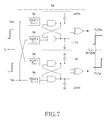
- FIG. 7 is a block diagram illustrating a structure of a TA according to an exemplary embodiment of the present invention.
- a TA 700 receives, as input signals, F REF and PI(n) which is selected by a MUX in a coarse TDC, amplifies a time interval T D between the PI(n) and the F REF widely in the time domain, and multiplies the time interval T D by a gain TA of the TA 700 (T D ⁇ TA).
- the TA 700 includes two latches 710 and 720 , and delay units # 1 through # 4 ( 702 through 708 ) having different delay times.
- the delay unit # 1 ( 702 ) and the delay unit # 4 ( 708 ) have a delay time T off+ ⁇
- the delay unit # 2 ( 704 ) and the delay unit # 3 ( 706 ) have a delay time T off .
- As ( ⁇ ) may be realized by a delay time caused by an inverter, i.e., a value much smaller than T off , a gain of the TA 700 may be increased. This will be described below.
- a gain of the TA 700 is represented as shown in Equation (1) below. That is, the gain of the TA 700 is inversely proportional to a transconductance (g m ) of NAND gates and a time difference ( ⁇ ) between two inputs to the latches 710 and 720 , and is proportional to output Capacitances (C) of the latches 710 and 720 .
- a capacitance of the C is reduced as much as possible and the time difference ⁇ between two inputs to the latches 710 and 720 is set to its minimum value to increase the gain of the TA.
- the time difference ⁇ between two inputs to the latches 710 and 720 is set to its minimum value to increase the gain of the TA.
- one of the two input signals is additionally delayed. For the delay, a delay time of an inverter is commonly used.
- exemplary embodiments of the present invention provide a TDC using a PI technique that uses a resistor auto-tuning scheme, and a TA that increases its gain with a time difference caused by the use of additional inverters.
- the TDC may have a high resolution at an RF input frequency.
Landscapes
- Physics & Mathematics (AREA)
- General Physics & Mathematics (AREA)
- Manipulation Of Pulses (AREA)
- Pulse Circuits (AREA)
- Stabilization Of Oscillater, Synchronisation, Frequency Synthesizers (AREA)
Abstract
Description
Claims (16)
Applications Claiming Priority (2)
| Application Number | Priority Date | Filing Date | Title |
|---|---|---|---|
| KR10-2010-0038067 | 2010-04-23 | ||
| KR1020100038067A KR101629970B1 (en) | 2010-04-23 | 2010-04-23 | A time to digital converter and proceesing method of the time to converter |
Publications (2)
| Publication Number | Publication Date |
|---|---|
| US20110260902A1 US20110260902A1 (en) | 2011-10-27 |
| US8330637B2 true US8330637B2 (en) | 2012-12-11 |
Family
ID=44815347
Family Applications (1)
| Application Number | Title | Priority Date | Filing Date |
|---|---|---|---|
| US13/089,558 Active 2031-07-28 US8330637B2 (en) | 2010-04-23 | 2011-04-19 | Time-to-digital converter and operation method thereof |
Country Status (2)
| Country | Link |
|---|---|
| US (1) | US8330637B2 (en) |
| KR (1) | KR101629970B1 (en) |
Cited By (6)
| Publication number | Priority date | Publication date | Assignee | Title |
|---|---|---|---|---|
| US20140062735A1 (en) * | 2012-08-30 | 2014-03-06 | Texas Instruments Incorporated | Asynchronous analog-to-digital converter having adapative reference control |
| US8754797B2 (en) * | 2012-08-30 | 2014-06-17 | Texas Instruments Incorporated | Asynchronous analog-to-digital converter having rate control |
| US20140210532A1 (en) * | 2013-01-29 | 2014-07-31 | Perceptia Devices Australia Pty Ltd. | Phase-Locked Loop Apparatus and Method |
| US20140247173A1 (en) * | 2013-03-01 | 2014-09-04 | Texas Instruments Incorporated | Asynchronous to synchronous sampling using akima algorithm |
| US9188961B1 (en) * | 2015-02-18 | 2015-11-17 | Micrel, Inc. | Time-to-digital converter |
| US20190111892A1 (en) * | 2017-10-13 | 2019-04-18 | Kabushiki Kaisha Tokai Rika Denki Seisakusho | Start switch device |
Families Citing this family (19)
| Publication number | Priority date | Publication date | Assignee | Title |
|---|---|---|---|---|
| KR101300828B1 (en) * | 2010-12-23 | 2013-08-29 | 건국대학교 산학협력단 | Time to digital converter using Successive Approximation and the method thereof |
| JP5703324B2 (en) * | 2013-03-13 | 2015-04-15 | 株式会社半導体理工学研究センター | Time amplification circuit and program for executing characteristic test thereof |
| US8957712B2 (en) | 2013-03-15 | 2015-02-17 | Qualcomm Incorporated | Mixed signal TDC with embedded T2V ADC |
| KR102013840B1 (en) | 2013-03-15 | 2019-08-23 | 삼성전자주식회사 | multi-phase generator |
| KR101506661B1 (en) | 2013-04-19 | 2015-03-31 | 연세대학교 산학협력단 | Time amplifier and method for controlling the same |
| CN103634010B (en) * | 2013-05-14 | 2016-09-21 | 中国科学院电子学研究所 | A kind of High-precision large-range time-to-digital converter based on difference charging |
| KR101624509B1 (en) * | 2014-03-27 | 2016-06-07 | 한국과학기술원 | Time to digital convertor and method of converting time to digital |
| KR101636610B1 (en) * | 2014-06-17 | 2016-07-06 | 인하대학교 산학협력단 | Method and Apparatus for Time Amplifier using Voltage Controlled Delay Line |
| US9746832B1 (en) * | 2016-09-09 | 2017-08-29 | Samsung Electronics Co., Ltd | System and method for time-to-digital converter fine-conversion using analog-to-digital converter (ADC) |
| US10108148B1 (en) * | 2017-04-14 | 2018-10-23 | Innophase Inc. | Time to digital converter with increased range and sensitivity |
| KR102029551B1 (en) * | 2017-12-19 | 2019-10-07 | 인하대학교 산학협력단 | Two-step time-to-digital converter using nand-gate ring oscillator time-amplifier |
| CN108549205B (en) * | 2018-04-12 | 2020-08-04 | 中国科学院微电子研究所 | A Two-Step Time-to-Digital Converter Based on Time Amplifier |
| CN109450398B (en) * | 2018-09-30 | 2022-11-29 | 南京邮电大学 | A Programmable Time Amplifier |
| KR102655132B1 (en) * | 2018-10-22 | 2024-04-04 | 이노페이즈 인크. | Time-to-digital converter with increased range and sensitivity |
| CN110515292B (en) * | 2019-08-12 | 2021-04-27 | 南京理工大学 | TDC circuit and measurement method based on bidirectional running ring carry chain |
| CN110824889B (en) * | 2019-11-08 | 2021-05-28 | 中山大学 | A Time-to-Digital Converter Based on a Novel Time Amplifier |
| EP4140039A1 (en) | 2020-04-24 | 2023-03-01 | Telefonaktiebolaget LM ERICSSON (PUBL) | Time to digital converter arrangement with increased detection range |
| TWI809918B (en) * | 2022-06-06 | 2023-07-21 | 國立中山大學 | Time amplifier |
| US12476780B2 (en) * | 2023-04-28 | 2025-11-18 | Analog Devices International Unlimited Company | Passive phase interpolator |
Citations (6)
| Publication number | Priority date | Publication date | Assignee | Title |
|---|---|---|---|---|
| US20090153377A1 (en) * | 2007-10-16 | 2009-06-18 | Mediatek Inc. | Time to digital converter with error protection |
| US7928888B1 (en) * | 2009-10-09 | 2011-04-19 | Industrial Technology Research Institute | Pipeline time-to-digital converter |
| US7932847B1 (en) * | 2009-12-04 | 2011-04-26 | Realtek Semiconductor Corp. | Hybrid coarse-fine time-to-digital converter |
| US7973578B2 (en) * | 2008-12-01 | 2011-07-05 | Samsung Electronics Co., Ltd. | Time-to-digital converter and all-digital phase-locked loop |
| US7978111B2 (en) * | 2008-03-03 | 2011-07-12 | Qualcomm Incorporated | High resolution time-to-digital converter |
| US8219343B2 (en) * | 2008-04-24 | 2012-07-10 | Realtek Semiconductor Corp. | Method and apparatus for calibrating a delay chain |
Family Cites Families (3)
| Publication number | Priority date | Publication date | Assignee | Title |
|---|---|---|---|---|
| KR100738236B1 (en) * | 2005-07-11 | 2007-07-12 | 엘지전자 주식회사 | Phase interpolation circuit. |
| JP5231068B2 (en) | 2008-03-31 | 2013-07-10 | 株式会社ダイヘン | High frequency power supply |
| KR100998475B1 (en) * | 2008-06-04 | 2010-12-06 | 에스케이텔레콤 주식회사 | Local wireless signal transmission apparatus and method using digital high frequency processing technology |
-
2010
- 2010-04-23 KR KR1020100038067A patent/KR101629970B1/en active Active
-
2011
- 2011-04-19 US US13/089,558 patent/US8330637B2/en active Active
Patent Citations (6)
| Publication number | Priority date | Publication date | Assignee | Title |
|---|---|---|---|---|
| US20090153377A1 (en) * | 2007-10-16 | 2009-06-18 | Mediatek Inc. | Time to digital converter with error protection |
| US7978111B2 (en) * | 2008-03-03 | 2011-07-12 | Qualcomm Incorporated | High resolution time-to-digital converter |
| US8219343B2 (en) * | 2008-04-24 | 2012-07-10 | Realtek Semiconductor Corp. | Method and apparatus for calibrating a delay chain |
| US7973578B2 (en) * | 2008-12-01 | 2011-07-05 | Samsung Electronics Co., Ltd. | Time-to-digital converter and all-digital phase-locked loop |
| US7928888B1 (en) * | 2009-10-09 | 2011-04-19 | Industrial Technology Research Institute | Pipeline time-to-digital converter |
| US7932847B1 (en) * | 2009-12-04 | 2011-04-26 | Realtek Semiconductor Corp. | Hybrid coarse-fine time-to-digital converter |
Cited By (14)
| Publication number | Priority date | Publication date | Assignee | Title |
|---|---|---|---|---|
| US8754797B2 (en) * | 2012-08-30 | 2014-06-17 | Texas Instruments Incorporated | Asynchronous analog-to-digital converter having rate control |
| US20140062735A1 (en) * | 2012-08-30 | 2014-03-06 | Texas Instruments Incorporated | Asynchronous analog-to-digital converter having adapative reference control |
| US8830106B2 (en) * | 2012-08-30 | 2014-09-09 | Texas Instruments Incorporated | Asynchronous analog-to-digital converter having adapative reference control |
| US8994423B2 (en) * | 2013-01-29 | 2015-03-31 | Perceptia Devices Australia, Pty Ltd. | Phase-locked loop apparatus and method |
| US20140210532A1 (en) * | 2013-01-29 | 2014-07-31 | Perceptia Devices Australia Pty Ltd. | Phase-Locked Loop Apparatus and Method |
| US9184761B2 (en) * | 2013-03-01 | 2015-11-10 | Texas Instruments Incorporated | Asynchronous to synchronous sampling using Akima algorithm |
| US20140247173A1 (en) * | 2013-03-01 | 2014-09-04 | Texas Instruments Incorporated | Asynchronous to synchronous sampling using akima algorithm |
| US9188961B1 (en) * | 2015-02-18 | 2015-11-17 | Micrel, Inc. | Time-to-digital converter |
| WO2016133566A1 (en) * | 2015-02-18 | 2016-08-25 | Micrel, Inc. | Time-to-digital converter |
| TWI568195B (en) * | 2015-02-18 | 2017-01-21 | 麥奎爾股份有限公司 | Time-to-digital converter |
| US20190111892A1 (en) * | 2017-10-13 | 2019-04-18 | Kabushiki Kaisha Tokai Rika Denki Seisakusho | Start switch device |
| US10518749B2 (en) * | 2017-10-13 | 2019-12-31 | Kabushiki Kaisha Tokai Rika Denki Seisakusho | Start switch device |
| US11161478B2 (en) | 2017-10-13 | 2021-11-02 | Kabushiki Kaisha Tokai Rika Denki Seisakusho | Start switch device |
| US11679739B2 (en) | 2017-10-13 | 2023-06-20 | Kabushiki Kaisha Tokai Rika Denki Seisakusho | Start switch device |
Also Published As
| Publication number | Publication date |
|---|---|
| KR101629970B1 (en) | 2016-06-13 |
| KR20110118458A (en) | 2011-10-31 |
| US20110260902A1 (en) | 2011-10-27 |
Similar Documents
| Publication | Publication Date | Title |
|---|---|---|
| US8330637B2 (en) | Time-to-digital converter and operation method thereof | |
| US10523219B2 (en) | Phase locked loop and control method therefor | |
| US7973578B2 (en) | Time-to-digital converter and all-digital phase-locked loop | |
| US9178497B2 (en) | Precision oscillator with temperature compensation | |
| US8264260B2 (en) | Delay locked loop and method of driving delay locked loop | |
| US10164574B2 (en) | Method for generating a plurality of oscillating signals with different phases and associated circuit and local oscillator | |
| WO2011001652A1 (en) | Pll circuit, and radio communication device equipped therewith | |
| EP2264902A1 (en) | Analogue/digital delay locked loop | |
| US11841738B2 (en) | Multi-phase clock signal phase difference detection and calculation circuit and method and digital phase modulation system | |
| US8085071B2 (en) | Phase-locked loop circuit and delay-locked loop circuit | |
| US9698807B1 (en) | Time signal conversion using dual time-based digital-to-analog converters | |
| US20170201259A1 (en) | Digital phase locked loop and method of driving the same | |
| US10447253B2 (en) | High performance PLL based on PVT independent stable oscillator | |
| US6348823B1 (en) | Digital controlled oscillating circuit of digital phase lock loops | |
| US20140347109A1 (en) | Hybrid phase-locked loops | |
| US20150229318A1 (en) | Oscillator circuit and frequency synthesizer | |
| JP2010021686A (en) | Digital phase detector and digital phase-locked loop circuit | |
| US8872558B1 (en) | Hybrid phase-locked loops | |
| US9614535B2 (en) | PLL circuit, method, and electronic apparatus | |
| Buhr et al. | A 10 bit phase-interpolator-based digital-to-phase converter for accurate time synchronization in Ethernet applications | |
| Huang et al. | A time-to-digital converter based AFC for wideband frequency synthesizer | |
| KR100905836B1 (en) | Phase locked loop with improved loop stability | |
| US10177752B2 (en) | Frequency comparator and early-late detector | |
| US12537533B2 (en) | Asynchronous successive approximation register with asynchronous clock control | |
| Toi et al. | Tracking PVT variations of Pulse Width Controlled PLL using variable-length ring oscillator |
Legal Events
| Date | Code | Title | Description |
|---|---|---|---|
| AS | Assignment |
Owner name: KONKUK UNIVERSITY INDUSTRY COOPERATION CORP., KORE Free format text: ASSIGNMENT OF ASSIGNORS INTEREST;ASSIGNORS:LEE, JAE-SUP;LEE, KANG-YOON;PARK, AN-SOO;AND OTHERS;REEL/FRAME:026149/0566 Effective date: 20110419 Owner name: SAMSUNG ELECTRONICS CO., LTD., KOREA, REPUBLIC OF Free format text: ASSIGNMENT OF ASSIGNORS INTEREST;ASSIGNORS:LEE, JAE-SUP;LEE, KANG-YOON;PARK, AN-SOO;AND OTHERS;REEL/FRAME:026149/0566 Effective date: 20110419 |
|
| STCF | Information on status: patent grant |
Free format text: PATENTED CASE |
|
| FEPP | Fee payment procedure |
Free format text: PAYOR NUMBER ASSIGNED (ORIGINAL EVENT CODE: ASPN); ENTITY STATUS OF PATENT OWNER: LARGE ENTITY |
|
| FPAY | Fee payment |
Year of fee payment: 4 |
|
| MAFP | Maintenance fee payment |
Free format text: PAYMENT OF MAINTENANCE FEE, 8TH YEAR, LARGE ENTITY (ORIGINAL EVENT CODE: M1552); ENTITY STATUS OF PATENT OWNER: LARGE ENTITY Year of fee payment: 8 |
|
| MAFP | Maintenance fee payment |
Free format text: PAYMENT OF MAINTENANCE FEE, 12TH YEAR, LARGE ENTITY (ORIGINAL EVENT CODE: M1553); ENTITY STATUS OF PATENT OWNER: LARGE ENTITY Year of fee payment: 12 |