US8324071B2 - Method for forming silicon film, method for forming pn junction and pn junction formed using the same - Google Patents
Method for forming silicon film, method for forming pn junction and pn junction formed using the same Download PDFInfo
- Publication number
- US8324071B2 US8324071B2 US12/458,665 US45866509A US8324071B2 US 8324071 B2 US8324071 B2 US 8324071B2 US 45866509 A US45866509 A US 45866509A US 8324071 B2 US8324071 B2 US 8324071B2
- Authority
- US
- United States
- Prior art keywords
- metal pattern
- doped layer
- substrate
- forming
- layer
- Prior art date
- Legal status (The legal status is an assumption and is not a legal conclusion. Google has not performed a legal analysis and makes no representation as to the accuracy of the status listed.)
- Expired - Fee Related, expires
Links
- 238000000034 method Methods 0.000 title claims abstract description 64
- XUIMIQQOPSSXEZ-UHFFFAOYSA-N Silicon Chemical compound [Si] XUIMIQQOPSSXEZ-UHFFFAOYSA-N 0.000 title claims abstract description 50
- 229910052710 silicon Inorganic materials 0.000 title claims abstract description 48
- 239000010703 silicon Substances 0.000 title claims abstract description 48
- 229910052751 metal Inorganic materials 0.000 claims abstract description 145
- 239000002184 metal Substances 0.000 claims abstract description 145
- 239000000758 substrate Substances 0.000 claims abstract description 95
- 229910021417 amorphous silicon Inorganic materials 0.000 claims description 22
- 238000005229 chemical vapour deposition Methods 0.000 claims description 13
- 238000010438 heat treatment Methods 0.000 claims description 11
- 229910021420 polycrystalline silicon Inorganic materials 0.000 abstract description 21
- 239000000463 material Substances 0.000 description 12
- 239000011521 glass Substances 0.000 description 5
- BLRPTPMANUNPDV-UHFFFAOYSA-N Silane Chemical compound [SiH4] BLRPTPMANUNPDV-UHFFFAOYSA-N 0.000 description 4
- 230000015572 biosynthetic process Effects 0.000 description 4
- 238000004519 manufacturing process Methods 0.000 description 4
- 238000002513 implantation Methods 0.000 description 3
- 229910052581 Si3N4 Inorganic materials 0.000 description 2
- VYPSYNLAJGMNEJ-UHFFFAOYSA-N Silicium dioxide Chemical compound O=[Si]=O VYPSYNLAJGMNEJ-UHFFFAOYSA-N 0.000 description 2
- XLOMVQKBTHCTTD-UHFFFAOYSA-N Zinc monoxide Chemical compound [Zn]=O XLOMVQKBTHCTTD-UHFFFAOYSA-N 0.000 description 2
- 238000002425 crystallisation Methods 0.000 description 2
- -1 e.g. Chemical compound 0.000 description 2
- 238000000623 plasma-assisted chemical vapour deposition Methods 0.000 description 2
- 238000004151 rapid thermal annealing Methods 0.000 description 2
- 229910052814 silicon oxide Inorganic materials 0.000 description 2
- XYFCBTPGUUZFHI-UHFFFAOYSA-N Phosphine Chemical compound P XYFCBTPGUUZFHI-UHFFFAOYSA-N 0.000 description 1
- 239000004020 conductor Substances 0.000 description 1
- 239000013078 crystal Substances 0.000 description 1
- ZOCHARZZJNPSEU-UHFFFAOYSA-N diboron Chemical compound B#B ZOCHARZZJNPSEU-UHFFFAOYSA-N 0.000 description 1
- 238000004050 hot filament vapor deposition Methods 0.000 description 1
- 239000007943 implant Substances 0.000 description 1
- AMGQUBHHOARCQH-UHFFFAOYSA-N indium;oxotin Chemical compound [In].[Sn]=O AMGQUBHHOARCQH-UHFFFAOYSA-N 0.000 description 1
- 239000011810 insulating material Substances 0.000 description 1
- 238000005224 laser annealing Methods 0.000 description 1
- 229910021424 microcrystalline silicon Inorganic materials 0.000 description 1
- 238000012986 modification Methods 0.000 description 1
- 230000004048 modification Effects 0.000 description 1
- 229910003465 moissanite Inorganic materials 0.000 description 1
- 229910052750 molybdenum Inorganic materials 0.000 description 1
- 229910021421 monocrystalline silicon Inorganic materials 0.000 description 1
- 229910000077 silane Inorganic materials 0.000 description 1
- 229910010271 silicon carbide Inorganic materials 0.000 description 1
- HQVNEWCFYHHQES-UHFFFAOYSA-N silicon nitride Chemical compound N12[Si]34N5[Si]62N3[Si]51N64 HQVNEWCFYHHQES-UHFFFAOYSA-N 0.000 description 1
- 239000013589 supplement Substances 0.000 description 1
- 238000002230 thermal chemical vapour deposition Methods 0.000 description 1
- 229910052721 tungsten Inorganic materials 0.000 description 1
- 239000011787 zinc oxide Substances 0.000 description 1
Images


Classifications
-
- H—ELECTRICITY
- H01—ELECTRIC ELEMENTS
- H01L—SEMICONDUCTOR DEVICES NOT COVERED BY CLASS H10
- H01L21/00—Processes or apparatus adapted for the manufacture or treatment of semiconductor or solid state devices or of parts thereof
- H01L21/02—Manufacture or treatment of semiconductor devices or of parts thereof
- H01L21/02104—Forming layers
- H01L21/02365—Forming inorganic semiconducting materials on a substrate
- H01L21/02518—Deposited layers
- H01L21/0257—Doping during depositing
- H01L21/02573—Conductivity type
-
- C—CHEMISTRY; METALLURGY
- C23—COATING METALLIC MATERIAL; COATING MATERIAL WITH METALLIC MATERIAL; CHEMICAL SURFACE TREATMENT; DIFFUSION TREATMENT OF METALLIC MATERIAL; COATING BY VACUUM EVAPORATION, BY SPUTTERING, BY ION IMPLANTATION OR BY CHEMICAL VAPOUR DEPOSITION, IN GENERAL; INHIBITING CORROSION OF METALLIC MATERIAL OR INCRUSTATION IN GENERAL
- C23C—COATING METALLIC MATERIAL; COATING MATERIAL WITH METALLIC MATERIAL; SURFACE TREATMENT OF METALLIC MATERIAL BY DIFFUSION INTO THE SURFACE, BY CHEMICAL CONVERSION OR SUBSTITUTION; COATING BY VACUUM EVAPORATION, BY SPUTTERING, BY ION IMPLANTATION OR BY CHEMICAL VAPOUR DEPOSITION, IN GENERAL
- C23C16/00—Chemical coating by decomposition of gaseous compounds, without leaving reaction products of surface material in the coating, i.e. chemical vapour deposition [CVD] processes
- C23C16/22—Chemical coating by decomposition of gaseous compounds, without leaving reaction products of surface material in the coating, i.e. chemical vapour deposition [CVD] processes characterised by the deposition of inorganic material, other than metallic material
- C23C16/24—Deposition of silicon only
-
- H—ELECTRICITY
- H01—ELECTRIC ELEMENTS
- H01L—SEMICONDUCTOR DEVICES NOT COVERED BY CLASS H10
- H01L21/00—Processes or apparatus adapted for the manufacture or treatment of semiconductor or solid state devices or of parts thereof
- H01L21/02—Manufacture or treatment of semiconductor devices or of parts thereof
- H01L21/02104—Forming layers
- H01L21/02365—Forming inorganic semiconducting materials on a substrate
- H01L21/02367—Substrates
- H01L21/0237—Materials
- H01L21/02422—Non-crystalline insulating materials, e.g. glass, polymers
-
- H—ELECTRICITY
- H01—ELECTRIC ELEMENTS
- H01L—SEMICONDUCTOR DEVICES NOT COVERED BY CLASS H10
- H01L21/00—Processes or apparatus adapted for the manufacture or treatment of semiconductor or solid state devices or of parts thereof
- H01L21/02—Manufacture or treatment of semiconductor devices or of parts thereof
- H01L21/02104—Forming layers
- H01L21/02365—Forming inorganic semiconducting materials on a substrate
- H01L21/02367—Substrates
- H01L21/0237—Materials
- H01L21/02425—Conductive materials, e.g. metallic silicides
-
- H—ELECTRICITY
- H01—ELECTRIC ELEMENTS
- H01L—SEMICONDUCTOR DEVICES NOT COVERED BY CLASS H10
- H01L21/00—Processes or apparatus adapted for the manufacture or treatment of semiconductor or solid state devices or of parts thereof
- H01L21/02—Manufacture or treatment of semiconductor devices or of parts thereof
- H01L21/02104—Forming layers
- H01L21/02365—Forming inorganic semiconducting materials on a substrate
- H01L21/02518—Deposited layers
- H01L21/02521—Materials
- H01L21/02524—Group 14 semiconducting materials
- H01L21/02532—Silicon, silicon germanium, germanium
-
- H—ELECTRICITY
- H01—ELECTRIC ELEMENTS
- H01L—SEMICONDUCTOR DEVICES NOT COVERED BY CLASS H10
- H01L21/00—Processes or apparatus adapted for the manufacture or treatment of semiconductor or solid state devices or of parts thereof
- H01L21/02—Manufacture or treatment of semiconductor devices or of parts thereof
- H01L21/02104—Forming layers
- H01L21/02365—Forming inorganic semiconducting materials on a substrate
- H01L21/02612—Formation types
- H01L21/02617—Deposition types
- H01L21/0262—Reduction or decomposition of gaseous compounds, e.g. CVD
Definitions
- Embodiments of the present invention relate to a method for forming a silicon film, a method for forming a pn junction, and a pn junction formed using the same.
- a silicon structure can be classified into amorphous silicon, single crystal silicon, and polycrystalline silicon depending on the crystal structure.
- Methods for forming polycrystalline silicon include a crystallization method and a direct growth method.
- amorphous silicon is changed into polycrystalline silicon by excimer laser annealing (ELA) or rapid thermal annealing (RTA).
- polycrystalline silicon is directly grown on a substrate by a chemical vapor deposition (CVD) method.
- CVD chemical vapor deposition
- Polycrystalline silicon may be grown on a glass substrate using a thermal CVD method, a hot filament CVD method, or a very high frequency CVD method.
- Embodiments of the present invention provide a method for forming a silicon film made of polycrystalline silicon using a microheater, a method for forming a pn junction, and a pn junction formed using the same.
- a method for forming a silicon film may include providing a microheater including a substrate and a metal pattern spaced apart from the substrate; applying a voltage to the metal pattern to heat the metal pattern; and exposing the microheater to a source gas containing silicon to form a silicon film on the metal pattern.
- a method for forming a pn junction may include providing a microheater including a substrate, a conductive layer on the substrate, and a metal pattern spaced apart from the substrate; and forming a pn junction between the metal pattern and the conductive layer by applying a voltage to the metal pattern to heat the metal pattern.
- a pn junction may include a microheater including a substrate, a conductive layer on the substrate, and a metal pattern spaced apart from the substrate; and a first doped layer and a second doped layer between the conductive layer and the metal pattern. At least one of the first doped layer and the second doped layer may be grown on the metal pattern.
- FIGS. 1-8E represent non-limiting, embodiments of the present invention as described herein.
- FIG. 1 is a perspective view illustrating a microheater according to an embodiment of the present invention
- FIGS. 2A to 2C are sectional views illustrating a method for forming a silicon film according to an embodiment of the present invention
- FIGS. 3A to 3C are sectional views illustrating a method for forming a pn junction according to an embodiment of the present invention
- FIGS. 4A to 4C are sectional views illustrating a method for forming a pn junction according to an embodiment of the present invention
- FIGS. 5A to 5C are sectional views illustrating a method for forming a pn junction according to an embodiment of the present invention
- FIGS. 6A to 6C are sectional views illustrating a method for forming a pn junction according to an embodiment of the present invention
- FIGS. 7A to 7C are sectional views illustrating a method for forming a pn junction according to an embodiment of the present invention.
- FIGS. 8A to 8E are sectional views illustrating a method for forming a pn junction according to an embodiment of the present invention.
- first, second, third etc. may be used herein to describe various elements, components, regions, layers and/or sections, these elements, components, regions, layers and/or sections should not be limited by these terms. These terms are only used to distinguish one element, component, region, layer or section from another region, layer or section. Thus, a first element, component, region, layer or section discussed below could be termed a second element, component, region, layer or section without departing from the teachings of embodiments.
- spatially relative terms e.g., “beneath,” “below,” “lower,” “above,” “upper” and the like, may be used herein for ease of description to describe one element or feature's relationship to another element(s) or feature(s) as illustrated in the figures. It will be understood that the spatially relative terms are intended to encompass different orientations of the device in use or operation in addition to the orientation depicted in the figures. For example, if the device in the figures is turned over, elements described as “below” or “beneath” other elements or features would be oriented “above” the other elements or features. Thus, the exemplary term “below” may encompass both an orientation of above and below. The device may be otherwise oriented (rotated 90 degrees or at other orientations) and the spatially relative descriptors used herein interpreted accordingly.
- Embodiments are described herein with reference to cross-sectional illustrations that are schematic illustrations of idealized embodiments (and intermediate structures). As such, variations from the shapes of the illustrations as a result, for example, of manufacturing techniques and/or tolerances, are to be expected. Thus, embodiments should not be construed as limited to the particular shapes of regions illustrated herein but are to include deviations in shapes that result, for example, from manufacturing. For example, an implanted region illustrated as a rectangle may, typically, have rounded or curved features and/or a gradient of implant concentration at its edges rather than a binary change from implanted to non-implanted region. Likewise, a buried region formed by implantation may result in some implantation in the region between the buried region and the surface through which the implantation takes place. Thus, the regions illustrated in the figures are schematic in nature and their shapes are not intended to illustrate the actual shape of a region of a device and are not intended to limit the scope of example.
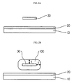
- FIG. 1 is a perspective view illustrating a microheater according to an embodiment of the present invention.
- the microheater may include a substrate 10 and a metal pattern 30 spaced apart from the substrate 10 .
- the substrate 10 may be made of a glass material.
- radiant heat for example, visible rays or infrared rays
- the substrate 10 may be manufactured to have a relatively large area.
- the metal pattern 30 may be formed above the substrate 10 to be spaced apart from the substrate 10 .
- the metal pattern 30 may be linear to extend on the substrate 10 in a direction.
- the shape of the metal pattern 30 is not limited to the above but may be different polygons or closed surfaces.
- the metal pattern 30 may be made of Mo, W, or SiC. When a voltage is applied to the metal pattern 30 , the metal pattern 30 may emit light and heat.
- each of the substrate 10 and the metal pattern 30 may include at least one material layer (not shown) formed on the surface thereof.
- formation of a silicon film on the substrate 10 may mean that the silicon film is formed on at least one material layer previously formed on the substrate 10 .
- At least one supporting unit 40 positioned between the metal pattern 30 and the substrate 10 may support the metal pattern 30 with the metal pattern 30 spaced apart from the substrate 10 .
- the supporting unit 40 may be made of a material having a relatively small heat conduction rate in order to prevent or reduce the loss of heat generated by the metal pattern 30 .
- the supporting unit 40 may be formed of an insulating material, e.g., silicon oxide (SiO x ) or silicon nitride (for example, Si 3 N 4 ).
- a conductive layer 20 may be formed on the substrate 10 .
- the metal pattern 30 and the conductive layer 20 may be used as an upper electrode and a lower electrode, respectively, when the microheater is applied to a device.
- the conductive layer 20 may be made of a transparent conductive material.
- the conductive layer 20 may be made of indium tin oxide (ITO), zinc oxide, or other suitable materials.
- FIGS. 2A to 2C are sectional views illustrating a method for forming a silicon film according to an embodiment of the present invention.
- a microheater including a substrate 10 and a metal pattern 30 spaced apart from the substrate 10 may be provided.
- a conductive layer 20 may be formed on the substrate 10 .
- a silicon film 100 may be formed on the metal pattern 30 .
- the silicon film 100 may be formed by applying a voltage to the metal pattern 30 to heat the metal pattern 30 and by exposing the heated metal pattern 30 to a source gas.
- the microheater including the metal pattern 30 may be positioned in a vacuum chamber and the source gas may be injected into the chamber so that the metal pattern 30 may be exposed to the source gas.
- the source gas may be a material including silicon, e.g., silane (SiH 4 ).
- the heating temperature of the metal pattern 30 may be equal to or above a first temperature.
- the first temperature may refer to the minimum temperature at which the metal pattern 30 is heated so that the silicon film 100 may be grown on the metal pattern 30 .
- the first temperature may be about 600° C.
- the source gas When the source gas contacts the surface of the metal pattern 30 heated at a temperature equal to or above the first temperature, the source gas may be decomposed on the surface of the metal pattern 30 so that the silicon film 100 may be grown on the metal pattern 30 .
- the silicon film 100 may be formed to an equal thickness t in all directions on the surface of the metal pattern 30 .
- the silicon film 100 may be grown on the metal pattern 30 at a speed of about 3 ⁇ m/min.
- the silicon film 100 may be made of polycrystalline silicon.
- polycrystalline silicon may mean an arbitrary silicon structure consisting of grains having a size no less than a predetermined or given size, including microcrystalline silicon.
- the silicon film 100 may consist of grains having a size no less than about 0.1 ⁇ m.
- the silicon film 100 is formed on the surface of the metal pattern 30 , even when a substrate made of glass is used, the silicon film 100 may be formed at a relatively high temperature. Therefore, the silicon film 100 consisting grains having a relatively large size may be obtained.
- the silicon film 100 on the metal pattern 30 may contact the conductive layer 20 .
- the metal pattern 30 and the conductive layer 20 may be used as an upper electrode and a lower electrode for applying power to the silicon film 100 , respectively.
- a silicon film 100 ′ may be formed on the substrate 10 at the same time as the silicon film 100 is formed on the surface of the metal pattern 30 .
- the heating temperature of the metal pattern 30 may be equal to or above a second temperature.
- the second temperature may refer to the minimum temperature at which the metal pattern 30 is exposed to the source gas so that a layer made of silicon may be formed on the substrate 10 as well as on the metal pattern 30 .
- the second temperature may be higher than the first temperature.
- the second temperature may be about 900° C.
- the silicon film 100 may be formed only on the metal pattern 30 .
- the source gas may be decomposed on the surface of the metal pattern 30 , so that the silicon film 100 may be formed on the metal pattern 30 and, at the same time, the silicon film 100 ′ may be formed on the substrate 10 by the silicon molecules that constitute the source gas.
- the silicon film 100 on the metal pattern 30 is made of polycrystalline silicon
- the silicon film 100 ′ on the substrate 10 may be made of amorphous silicon.
- FIGS. 3A to 3C are sectional views illustrating a method for forming a pn junction according to an embodiment of the present invention.
- the pn junction may mean various structures in which pn junction characteristics are used, e.g., p/i (intrinsic Si)/n, n/p/n, p/n/p/n, and p/i/n/p/i/n, as well as a p/n or n/p structure consisting of one p-type doped layer and one n-type doped layer.
- the microheater including the substrate 10 , the conductive layer 20 on the substrate, and the metal pattern 30 spaced apart from the substrate 10 is provided.
- a first doped layer 201 may be grown on the metal pattern 30 .
- the first doped layer 201 may be made of n-type or p-type doped silicon.
- the first doped layer 201 may be formed by applying a voltage to the metal pattern 30 to heat the metal pattern 30 and by exposing the heated metal pattern 30 to the source gas and a first doping gas.
- the metal pattern 30 may be heated at a temperature no less than the first temperature.
- the source gas may be a material including silicon, e.g., SiH 4 .
- the first doping gas may be a material for doping the first doped layer 201 as p-type or n-type.
- the first doping gas may be phosphine (PH 3 ) when the first doped layer 201 is an n-type doped layer.
- an intrinsic layer 202 may be grown on the first doped layer 201 .
- the intrinsic layer 202 may be formed by exposing the metal pattern 30 on which the first doped layer 201 is formed to the source gas.
- the metal pattern 30 may be maintained at a temperature no less than the first temperature. Because the intrinsic layer 202 is formed using only the source gas without the doping gas, the intrinsic layer 202 may be made of intrinsic silicon.
- a second doped layer 203 may be grown on the metal pattern 30 on which the intrinsic layer 202 is formed.
- the second doped layer 203 may be grown until the second doped layer 203 contacts the conductive layer 20 on the substrate 10 .
- the second doped layer 203 may be formed by exposing the heated metal pattern 30 to the source gas and a second doping gas.
- the second doping gas may be a material for doping the second doped layer 203 as p-type or n-type.
- the second doping gas may be diborane (B 2 H 6 ) when the second doped layer 203 is a p-type doped layer.
- the first doped layer 201 and the second doped layer 203 may be doped as different types. As a result, a pn junction having a p/i/n or n/i/p structure consisting of the first doped layer 201 , the intrinsic layer 202 , and the second doped layer 203 may be formed.
- formation of the intrinsic layer 202 described above with reference to FIG. 3B may be omitted.
- the second doped layer 203 is directly grown on the first doped layer 201 , a pn junction of a p/n or n/p structure may be formed.
- the first and second doped layer 201 , 203 may be made of polycrystalline silicon. Therefore, a relatively higher quality pn junction may be obtained as compared to when the pn junction is formed on a glass substrate. Further, the pn junction may be formed at a relatively high speed.
- the pn junction may be used for a device, e.g., a light emitting diode (LED), a solar cell, and a photodiode.
- FIGS. 4A to 4C are sectional views illustrating a method for forming a pn junction according to an embodiment of the present invention.
- the microheater including the substrate 10 , the conductive layer 20 on the substrate 10 , and the metal pattern 30 spaced apart from the substrate 10 may be provided and a first doped layer 301 may be formed on the substrate 10 .
- the first doped layer 301 may be made of amorphous silicon.
- the first doped layer 301 may be formed by a chemical vapor deposition (CVD) method or other suitable methods.
- the first doped layer 301 may be formed by a plasma enhanced CVD (PECVD) method.
- PECVD plasma enhanced CVD
- a second doped layer 302 may be grown on the metal pattern 30 .
- the second doped layer 302 may be formed by applying a voltage to the metal pattern 30 to heat the metal pattern 30 and by exposing the heated metal pattern 30 to the source gas and a second doping gas.
- the second doped layer 302 may be doped to be of a different type from the first doped layer 301 .
- an intrinsic layer 303 may be grown on the second doped layer 302 .
- the intrinsic layer 303 may be formed by exposing the metal pattern 30 on which the second doped layer 302 is formed to the source gas.
- the intrinsic layer 303 may be grown until the intrinsic layer 303 contacts the first doped layer 301 on the substrate 10 .
- a pn junction of a p/i/n or n/i/p structure consisting of the first doped layer 301 , the intrinsic layer 303 , and the second doped layer 302 may be formed.
- the first doped layer 301 may be made of amorphous silicon and the intrinsic layer 303 and the second doped layer 302 may be made of polycrystalline silicon.
- formation of the above-described intrinsic layer 302 may be omitted and the second doped layer 302 may be grown on the metal pattern 30 to contact the first doped layer 301 so that the pn junction of the n/p or p/n structure may be formed.
- FIGS. 5A to 5C are sectional views illustrating a method for forming a pn junction according to an embodiment of the present invention.
- the microheater including the substrate 10 , the conductive layer 20 on the substrate 10 , and the metal pattern 30 spaced apart from the substrate 10 may be provided and a first doped layer 401 may be formed on the substrate 10 .
- the first doped layer 401 may be made of n-type or p-type doped amorphous silicon.
- an intrinsic layer 402 may be grown on the substrate 10 on which the first doped layer 401 is formed.
- the first doped layer 401 and the intrinsic layer 402 may be formed by a CVD method or other suitable methods.
- a second doped layer 403 may be grown on the metal pattern 30 .
- the second doped layer 403 may be formed by applying a voltage to the metal pattern 30 to heat the metal pattern 30 and by exposing the heated metal pattern 30 to the source gas and the second doping gas.
- the metal pattern 30 may be heated at a temperature no less than the first temperature.
- the second doped layer 403 may be grown until the second doped layer 403 contacts the intrinsic layer 402 on the substrate 10 .
- the second doped layer 403 may be doped to be of a different type from the first doped layer 401 .
- a pn junction of a p/i/n or n/i/p structure consisting of the first doped layer 401 , the intrinsic layer 402 , and the second doped layer 403 may be formed.
- the first doped layer 401 and the intrinsic layer 402 may be made of amorphous silicon and the second doped layer 403 may be made of polycrystalline silicon.
- the layer made of amorphous silicon is combined with the layer made of polycrystalline silicon to form the pn junction.
- FIGS. 6A to 6C are sectional views illustrating a method for forming a pn junction according to an embodiment of the present invention.
- the microheater including the substrate 10 , the conductive layer 20 on the substrate 10 , and the metal pattern 30 spaced apart from the substrate 10 may be provided.
- a first doped layer 501 may be formed on the substrate 10 .
- the first doped layer 501 may be made of n-type or p-type doped amorphous silicon.
- the first doped layer 501 may be formed by a CVD method or other suitable methods.
- a second doped layer 502 may be formed on the metal pattern 30 .
- a layer made of polycrystalline silicon may be formed on the metal pattern 30 and, at the same time, a layer made of amorphous silicon may be formed on the substrate 10 . Therefore, by controlling the temperature of the metal pattern 30 to be between the first temperature and the second temperature or to be no less than the second temperature, a silicon film may be selectively formed on the substrate 10 .
- the metal pattern 30 may be heated at a temperature no less than the second temperature so that the second doped layer 502 may be formed on the metal pattern 30 and, at the same time, a second doped layer 502 ′ may be formed on the substrate 10 .
- the second doped layer 502 on the metal pattern 30 is made of polycrystalline silicon
- the second doped layer 502 ′ on the substrate 10 may be made of amorphous silicon.
- first doped layers 503 and 503 ′ may be formed on the substrate 10 and the metal pattern 30 , respectively.
- the first doped layers 503 and 503 ′ may be formed by exposing the heated metal pattern 30 to the source gas and the first doping gas.
- the metal pattern 30 may be maintained at a temperature no less than the second temperature.
- the first doped layers 503 and 503 ′ may be grown until the first doped layers 503 and 503 ′ contact each other.
- the temperature of the metal pattern 30 may be controlled to be between the first temperature and the second temperature so that the first doped layer 503 may be grown only on the metal pattern 30 .
- the grown first doped layer 503 may contact the second doped layer 502 ′ on the substrate 10 .
- a pn junction of a p/n-p/n or n/p-n/p structure consisting of the first doped layer 501 , the second doped layer 502 ′, the first doped layer 503 , and the second doped layer 502 may be formed.
- the first doped layer 501 and the second doped layer 502 ′ are made of amorphous silicon
- the first doped layer 503 and the second doped layer 502 may be made of polycrystalline silicon.
- the pn junction of the above structure may be used for manufacturing a tandem solar cell.
- FIGS. 7A to 7C are sectional views illustrating a method for forming a pn junction according to an embodiment of the present invention.
- the microheater including the substrate 10 , the conductive layer 20 on the substrate 10 , and the metal pattern 30 spaced apart from the substrate 10 may be provided and first doped layers 601 and 601 ′ may be grown on the substrate 10 and the metal pattern 30 , respectively.
- the heating temperature of the metal pattern 30 may be no less than the second temperature.
- intrinsic layers 602 and 602 ′ may be grown on the substrate 10 and the metal pattern 30 , respectively.
- the intrinsic layers 602 and 602 ′ may be formed by exposing the heated metal pattern 30 to the source gas.
- second doped layers 603 and 603 ′ may be grown on the substrate 10 and the metal pattern 30 , respectively.
- the second doped layers 603 and 603 ′ may be formed by exposing the heated metal pattern 30 to the source gas and the second doping gas.
- the second doped layers 603 and 603 ′ may be grown until the second doped layers 603 and 603 ′ contact each other.
- the metal pattern 30 may be maintained at a temperature no less than the second temperature.
- the heating temperature of the metal pattern 30 may be controlled to be between the first temperature and the second temperature so that the second doped layer 603 may be grown only on the metal pattern 30 .
- the second doped layer 603 may be grown until the second doped layer 603 contacts the intrinsic layer 602 ′ on the substrate 10 .
- a pn junction of an n/i/p/i/n or p/i/n/i/p structure consisting of the first doped layer 601 ′, the intrinsic layer 602 ′, the second doped layers 603 ′ and 603 , the intrinsic layer 602 , and the first doped layer 601 may be formed.
- the first doped layer 601 ′, the intrinsic layer 602 ′, and the second doped layer 603 ′ are made of amorphous silicon
- the second doped layer 603 , the intrinsic layer 602 , and the first doped layer 601 may be made of polycrystalline silicon.
- formation of the intrinsic layers 602 and 602 ′ described above with reference to FIG. 7B may be omitted.
- the second doped layers 603 and 603 ′ are directly grown on the first doped layers 601 and 601 ′, a pn junction of a p/n/p or n/p/n structure may be formed.
- FIGS. 8A to 8E are sectional views illustrating a method for forming a pn junction according to an embodiment of the present invention.
- the microheater including the substrate 10 , the conductive layer 20 on the substrate 10 , and the metal pattern 30 spaced apart from the substrate 10 may be provided and a first doped layer 701 may be formed on the substrate 10 .
- the first doped layer 701 may be made of n-type or p-type doped amorphous silicon and may be formed by a CVD method or other suitable methods.
- a second doped layer 702 may be grown on the metal pattern 30 .
- the second doped layer 702 may be doped to be of a different type from the first doped layer 701 .
- the second doped layer 702 may be grown by exposing the heated metal pattern 30 to the source gas and the second doping gas. The heating temperature of the metal pattern 30 may be between the first temperature and the second temperature.
- an intrinsic layer 703 may be grown on the metal pattern 30 by heating the metal pattern 30 at a temperature no less than the second temperature and by exposing the heated metal pattern 30 to the source gas.
- an intrinsic layer 703 ′ may be grown on the substrate 10 .
- the intrinsic layer 703 on the metal pattern 30 may be made of polycrystalline silicon and the intrinsic layer 703 ′ on the substrate 10 may be made of amorphous silicon.
- a first doped layer 704 may be grown on the metal pattern 30 .
- the first doped layer 704 may be grown by reducing the voltage applied to the metal pattern 30 to control the heating temperature of the metal pattern 30 to be between the first temperature and the second temperature and by exposing the metal pattern 30 to the source gas and the first doping gas.
- a second doped layer 705 may be formed on the substrate 10 .
- the second doped layer 705 may be made of amorphous silicon and may be formed by a CVD method or other suitable methods.
- the second doped layer 705 may be grown until the second doped layer 705 contacts the intrinsic layer 703 ′ on the metal pattern 30 .
- a pn junction of a p/i/n-p/i/n or n/i/p-n/i/p structure consisting of the first doped layer 701 , the intrinsic layer 703 ′, the second doped layer 705 , the first doped layer 704 , the intrinsic layer 703 , and the second doped layer 702 may be formed.
- the first doped layer 701 , the intrinsic layer 703 ′, and the second doped layer 705 may be made of amorphous silicon, and the first doped layer 704 , the intrinsic layer 703 , and the second doped layer 702 may be made of polycrystalline silicon.
- the pn junction of the above structure may be used for manufacturing the tandem solar cell.
Abstract
A method for forming a silicon film may be performed using a microheater including a substrate and a metal pattern spaced apart from the substrate. The silicon film may be formed on the metal pattern by applying a voltage to the metal pattern of the microheater to heat the metal pattern and by exposing the microheater to a source gas containing silicon. The silicon film may be made of polycrystalline silicon. A method for forming a pn junction may be performed using a microheater including a substrate, a conductive layer on the substrate, and a metal pattern spaced apart from the substrate. The pn junction may be formed between the metal pattern and the conductive layer by applying a voltage to the metal pattern of the microheater to heat the metal pattern. The pn junction may be made of polycrystalline silicon.
Description
This application claims priority under 35 U.S.C. §119 to Korean Patent Application No. 10-2009-0006118, filed on Jan. 23, 2009, in the Korean Intellectual Property Office (KIPO), the entire contents of which are herein incorporated by reference.
1. Field
Embodiments of the present invention relate to a method for forming a silicon film, a method for forming a pn junction, and a pn junction formed using the same.
2. Description of the Related Art
A silicon structure can be classified into amorphous silicon, single crystal silicon, and polycrystalline silicon depending on the crystal structure. Methods for forming polycrystalline silicon include a crystallization method and a direct growth method.
In the crystallization method, after forming amorphous silicon, amorphous silicon is changed into polycrystalline silicon by excimer laser annealing (ELA) or rapid thermal annealing (RTA).
In the direct growth method, polycrystalline silicon is directly grown on a substrate by a chemical vapor deposition (CVD) method. Polycrystalline silicon may be grown on a glass substrate using a thermal CVD method, a hot filament CVD method, or a very high frequency CVD method.
Embodiments of the present invention provide a method for forming a silicon film made of polycrystalline silicon using a microheater, a method for forming a pn junction, and a pn junction formed using the same.
According to an embodiment of the present invention, a method for forming a silicon film may include providing a microheater including a substrate and a metal pattern spaced apart from the substrate; applying a voltage to the metal pattern to heat the metal pattern; and exposing the microheater to a source gas containing silicon to form a silicon film on the metal pattern.
According to an embodiment of the present invention, a method for forming a pn junction may include providing a microheater including a substrate, a conductive layer on the substrate, and a metal pattern spaced apart from the substrate; and forming a pn junction between the metal pattern and the conductive layer by applying a voltage to the metal pattern to heat the metal pattern.
According to an embodiment of the present invention, a pn junction may include a microheater including a substrate, a conductive layer on the substrate, and a metal pattern spaced apart from the substrate; and a first doped layer and a second doped layer between the conductive layer and the metal pattern. At least one of the first doped layer and the second doped layer may be grown on the metal pattern.
Embodiments of the present invention will be more clearly understood from the following detailed description taken in conjunction with the accompanying drawings. FIGS. 1-8E represent non-limiting, embodiments of the present invention as described herein.
It should be noted that these Figures are intended to illustrate the general characteristics of methods, structure and/or materials utilized in certain embodiments and to supplement the written description provided below. These drawings are not, however, to scale and may not precisely reflect the precise structural or performance characteristics of any given embodiment, and should not be interpreted as defining or limiting the range of values or properties encompassed by embodiments. For example, the relative thicknesses and positioning of molecules, layers, regions and/or structural elements may be reduced or exaggerated for clarity. The use of similar or identical reference numbers in the various drawings is intended to indicate the presence of a similar or identical element or feature.
Embodiments now will be described more fully hereinafter with reference to the accompanying drawings, in which embodiments are shown. This disclosure may, however, be embodied in many different forms and should not be construed as limited to embodiments set forth therein. Rather, these embodiments are provided so that this disclosure will be thorough and complete, and will fully convey the scope of this disclosure to those skilled in the art. In the description, details of well-known features and techniques may be omitted to avoid unnecessarily obscuring the presented embodiments.
It will be understood that when an element or layer is referred to as being “on,” “connected to” or “coupled to” another element or layer, it may be directly on, connected or coupled to the other element or layer or intervening elements or layers may be present. In contrast, when an element is referred to as being “directly on,” “directly connected to” or “directly coupled to” another element or layer, there are no intervening elements or layers present. As used herein, the term “and/or” includes any and all combinations of one or more of the associated listed items.
It will be understood that, although the terms first, second, third etc. may be used herein to describe various elements, components, regions, layers and/or sections, these elements, components, regions, layers and/or sections should not be limited by these terms. These terms are only used to distinguish one element, component, region, layer or section from another region, layer or section. Thus, a first element, component, region, layer or section discussed below could be termed a second element, component, region, layer or section without departing from the teachings of embodiments.
Spatially relative terms, e.g., “beneath,” “below,” “lower,” “above,” “upper” and the like, may be used herein for ease of description to describe one element or feature's relationship to another element(s) or feature(s) as illustrated in the figures. It will be understood that the spatially relative terms are intended to encompass different orientations of the device in use or operation in addition to the orientation depicted in the figures. For example, if the device in the figures is turned over, elements described as “below” or “beneath” other elements or features would be oriented “above” the other elements or features. Thus, the exemplary term “below” may encompass both an orientation of above and below. The device may be otherwise oriented (rotated 90 degrees or at other orientations) and the spatially relative descriptors used herein interpreted accordingly.
Embodiments are described herein with reference to cross-sectional illustrations that are schematic illustrations of idealized embodiments (and intermediate structures). As such, variations from the shapes of the illustrations as a result, for example, of manufacturing techniques and/or tolerances, are to be expected. Thus, embodiments should not be construed as limited to the particular shapes of regions illustrated herein but are to include deviations in shapes that result, for example, from manufacturing. For example, an implanted region illustrated as a rectangle may, typically, have rounded or curved features and/or a gradient of implant concentration at its edges rather than a binary change from implanted to non-implanted region. Likewise, a buried region formed by implantation may result in some implantation in the region between the buried region and the surface through which the implantation takes place. Thus, the regions illustrated in the figures are schematic in nature and their shapes are not intended to illustrate the actual shape of a region of a device and are not intended to limit the scope of example.
The terminology used herein is for the purpose of describing particular embodiments only and is not intended to be limiting of this disclosure. As used herein, the singular forms “a”, “an” and “the” are intended to include the plural forms as well, unless the context clearly indicates otherwise. Furthermore, the use of the terms a, an, etc. does not denote a limitation of quantity, but rather denotes the presence of at least one of the referenced item. The use of the terms “first”, “second”, and the like does not imply any particular order, but they are included to identify individual elements. Moreover, the use of the terms first, second, etc. does not denote any order or importance, but rather the terms first, second, etc. are used to distinguish one element from another. It will be further understood that the terms “comprises” and/or “comprising”, or “includes” and/or “including” when used in this specification, specify the presence of stated features, regions, integers, steps, operations, elements, and/or components, but do not preclude the presence or addition of one or more other features, regions, integers, steps, operations, elements, components, and/or groups thereof.
Unless otherwise defined, all terms (including technical and scientific terms) used herein have the same meaning as commonly understood by one of ordinary skill in the art. It will be further understood that terms, such as those defined in commonly used dictionaries, should be interpreted as having a meaning that is consistent with their meaning in the context of the relevant art and the present disclosure, and will not be interpreted in an idealized or overly formal sense unless expressly so defined herein.
In the drawings, like reference numerals in the drawings denote like elements. The shape, size and regions, and the like, of the drawing may be exaggerated for clarity.
The metal pattern 30 may be formed above the substrate 10 to be spaced apart from the substrate 10. The metal pattern 30 may be linear to extend on the substrate 10 in a direction. However, the shape of the metal pattern 30 is not limited to the above but may be different polygons or closed surfaces. The metal pattern 30 may be made of Mo, W, or SiC. When a voltage is applied to the metal pattern 30, the metal pattern 30 may emit light and heat.
As used herein, each of the substrate 10 and the metal pattern 30 may include at least one material layer (not shown) formed on the surface thereof. For example, formation of a silicon film on the substrate 10 may mean that the silicon film is formed on at least one material layer previously formed on the substrate 10.
At least one supporting unit 40 positioned between the metal pattern 30 and the substrate 10 may support the metal pattern 30 with the metal pattern 30 spaced apart from the substrate 10. The supporting unit 40 may be made of a material having a relatively small heat conduction rate in order to prevent or reduce the loss of heat generated by the metal pattern 30. For example, the supporting unit 40 may be formed of an insulating material, e.g., silicon oxide (SiOx) or silicon nitride (for example, Si3N4).
A conductive layer 20 may be formed on the substrate 10. The metal pattern 30 and the conductive layer 20 may be used as an upper electrode and a lower electrode, respectively, when the microheater is applied to a device. The conductive layer 20 may be made of a transparent conductive material. For example, the conductive layer 20 may be made of indium tin oxide (ITO), zinc oxide, or other suitable materials.
Referring to FIG. 2B , a silicon film 100 may be formed on the metal pattern 30. The silicon film 100 may be formed by applying a voltage to the metal pattern 30 to heat the metal pattern 30 and by exposing the heated metal pattern 30 to a source gas. For example, the microheater including the metal pattern 30 may be positioned in a vacuum chamber and the source gas may be injected into the chamber so that the metal pattern 30 may be exposed to the source gas. The source gas may be a material including silicon, e.g., silane (SiH4).
The heating temperature of the metal pattern 30 may be equal to or above a first temperature. As used herein, the first temperature may refer to the minimum temperature at which the metal pattern 30 is heated so that the silicon film 100 may be grown on the metal pattern 30. For example, the first temperature may be about 600° C.
When the source gas contacts the surface of the metal pattern 30 heated at a temperature equal to or above the first temperature, the source gas may be decomposed on the surface of the metal pattern 30 so that the silicon film 100 may be grown on the metal pattern 30. The silicon film 100 may be formed to an equal thickness t in all directions on the surface of the metal pattern 30.
For example, when the metal pattern 30 is heated at a temperature of about 750° C. under a pressure of about 0.75 Torr using SiH4 of about 100 sccm as the source gas, the silicon film 100 may be grown on the metal pattern 30 at a speed of about 3 μm/min.
On the other hand, the silicon film 100 may be made of polycrystalline silicon. As used herein, polycrystalline silicon may mean an arbitrary silicon structure consisting of grains having a size no less than a predetermined or given size, including microcrystalline silicon. For example, the silicon film 100 may consist of grains having a size no less than about 0.1 μm.
Because the silicon film 100 is formed on the surface of the metal pattern 30, even when a substrate made of glass is used, the silicon film 100 may be formed at a relatively high temperature. Therefore, the silicon film 100 consisting grains having a relatively large size may be obtained.
The silicon film 100 on the metal pattern 30 may contact the conductive layer 20. When the silicon film 100 is applied to a device, the metal pattern 30 and the conductive layer 20 may be used as an upper electrode and a lower electrode for applying power to the silicon film 100, respectively.
Referring to FIG. 2 c, according to an embodiment of the present invention, a silicon film 100′ may be formed on the substrate 10 at the same time as the silicon film 100 is formed on the surface of the metal pattern 30.
The heating temperature of the metal pattern 30 may be equal to or above a second temperature. As used herein, the second temperature may refer to the minimum temperature at which the metal pattern 30 is exposed to the source gas so that a layer made of silicon may be formed on the substrate 10 as well as on the metal pattern 30. The second temperature may be higher than the first temperature. For example, the second temperature may be about 900° C.
That is, when the heating temperature of the metal pattern 30 is between the first temperature and the second temperature, as described above with reference to FIG. 2B , the silicon film 100 may be formed only on the metal pattern 30.
However, when the metal pattern 30 is heated at a temperature equal to or above the second temperature, the source gas may be decomposed on the surface of the metal pattern 30, so that the silicon film 100 may be formed on the metal pattern 30 and, at the same time, the silicon film 100′ may be formed on the substrate 10 by the silicon molecules that constitute the source gas. In an embodiment of the present invention, whereas the silicon film 100 on the metal pattern 30 is made of polycrystalline silicon, the silicon film 100′ on the substrate 10 may be made of amorphous silicon.
Referring to FIG. 3A , the microheater including the substrate 10, the conductive layer 20 on the substrate, and the metal pattern 30 spaced apart from the substrate 10 is provided. A first doped layer 201 may be grown on the metal pattern 30. The first doped layer 201 may be made of n-type or p-type doped silicon.
The first doped layer 201 may be formed by applying a voltage to the metal pattern 30 to heat the metal pattern 30 and by exposing the heated metal pattern 30 to the source gas and a first doping gas. The metal pattern 30 may be heated at a temperature no less than the first temperature.
The source gas may be a material including silicon, e.g., SiH4. The first doping gas may be a material for doping the first doped layer 201 as p-type or n-type. For example, the first doping gas may be phosphine (PH3) when the first doped layer 201 is an n-type doped layer.
Referring to FIG. 3B , an intrinsic layer 202 may be grown on the first doped layer 201. The intrinsic layer 202 may be formed by exposing the metal pattern 30 on which the first doped layer 201 is formed to the source gas. The metal pattern 30 may be maintained at a temperature no less than the first temperature. Because the intrinsic layer 202 is formed using only the source gas without the doping gas, the intrinsic layer 202 may be made of intrinsic silicon.
Referring to FIG. 3C , a second doped layer 203 may be grown on the metal pattern 30 on which the intrinsic layer 202 is formed. The second doped layer 203 may be grown until the second doped layer 203 contacts the conductive layer 20 on the substrate 10. The second doped layer 203 may be formed by exposing the heated metal pattern 30 to the source gas and a second doping gas. The second doping gas may be a material for doping the second doped layer 203 as p-type or n-type. For example, the second doping gas may be diborane (B2H6) when the second doped layer 203 is a p-type doped layer.
The first doped layer 201 and the second doped layer 203 may be doped as different types. As a result, a pn junction having a p/i/n or n/i/p structure consisting of the first doped layer 201, the intrinsic layer 202, and the second doped layer 203 may be formed.
According to another example embodiment of the present invention, formation of the intrinsic layer 202 described above with reference to FIG. 3B may be omitted. In embodiments, because the second doped layer 203 is directly grown on the first doped layer 201, a pn junction of a p/n or n/p structure may be formed.
According to the above-described method for forming the pn junction, because the first doped layer 201 and the second doped layer 203 are formed on the metal pattern 30 at a relatively high temperature, the first and second doped layer 201, 203 may be made of polycrystalline silicon. Therefore, a relatively higher quality pn junction may be obtained as compared to when the pn junction is formed on a glass substrate. Further, the pn junction may be formed at a relatively high speed. The pn junction may be used for a device, e.g., a light emitting diode (LED), a solar cell, and a photodiode.
Referring to FIG. 4B , a second doped layer 302 may be grown on the metal pattern 30. The second doped layer 302 may be formed by applying a voltage to the metal pattern 30 to heat the metal pattern 30 and by exposing the heated metal pattern 30 to the source gas and a second doping gas. The second doped layer 302 may be doped to be of a different type from the first doped layer 301.
Referring to FIG. 4C , an intrinsic layer 303 may be grown on the second doped layer 302. The intrinsic layer 303 may be formed by exposing the metal pattern 30 on which the second doped layer 302 is formed to the source gas. The intrinsic layer 303 may be grown until the intrinsic layer 303 contacts the first doped layer 301 on the substrate 10.
As a result, a pn junction of a p/i/n or n/i/p structure consisting of the first doped layer 301, the intrinsic layer 303, and the second doped layer 302 may be formed. The first doped layer 301 may be made of amorphous silicon and the intrinsic layer 303 and the second doped layer 302 may be made of polycrystalline silicon.
On the other hand, according to another embodiment of the present invention, referring to FIG. 4C , formation of the above-described intrinsic layer 302 may be omitted and the second doped layer 302 may be grown on the metal pattern 30 to contact the first doped layer 301 so that the pn junction of the n/p or p/n structure may be formed.
Referring to FIG. 5B , an intrinsic layer 402 may be grown on the substrate 10 on which the first doped layer 401 is formed. The first doped layer 401 and the intrinsic layer 402 may be formed by a CVD method or other suitable methods.
Referring to FIG. 5C , a second doped layer 403 may be grown on the metal pattern 30. The second doped layer 403 may be formed by applying a voltage to the metal pattern 30 to heat the metal pattern 30 and by exposing the heated metal pattern 30 to the source gas and the second doping gas. The metal pattern 30 may be heated at a temperature no less than the first temperature. The second doped layer 403 may be grown until the second doped layer 403 contacts the intrinsic layer 402 on the substrate 10.
The second doped layer 403 may be doped to be of a different type from the first doped layer 401. As a result, a pn junction of a p/i/n or n/i/p structure consisting of the first doped layer 401, the intrinsic layer 402, and the second doped layer 403 may be formed. The first doped layer 401 and the intrinsic layer 402 may be made of amorphous silicon and the second doped layer 403 may be made of polycrystalline silicon.
According to the methods for forming a pn junction described above with reference to FIGS. 4 and 5 , the layer made of amorphous silicon is combined with the layer made of polycrystalline silicon to form the pn junction.
Referring to FIG. 6B , a second doped layer 502 may be formed on the metal pattern 30. Meanwhile, when the metal pattern 30 is heated at a temperature no less than the second temperature, a layer made of polycrystalline silicon may be formed on the metal pattern 30 and, at the same time, a layer made of amorphous silicon may be formed on the substrate 10. Therefore, by controlling the temperature of the metal pattern 30 to be between the first temperature and the second temperature or to be no less than the second temperature, a silicon film may be selectively formed on the substrate 10.
Referring to FIG. 6B , the metal pattern 30 may be heated at a temperature no less than the second temperature so that the second doped layer 502 may be formed on the metal pattern 30 and, at the same time, a second doped layer 502′ may be formed on the substrate 10. Whereas the second doped layer 502 on the metal pattern 30 is made of polycrystalline silicon, the second doped layer 502′ on the substrate 10 may be made of amorphous silicon.
Referring to FIG. 6C , first doped layers 503 and 503′ may be formed on the substrate 10 and the metal pattern 30, respectively. The first doped layers 503 and 503′ may be formed by exposing the heated metal pattern 30 to the source gas and the first doping gas. The metal pattern 30 may be maintained at a temperature no less than the second temperature. The first doped layers 503 and 503′ may be grown until the first doped layers 503 and 503′ contact each other.
On the other hand, according to another embodiment of the present invention, after forming the second doped layers 502 and 502′, the temperature of the metal pattern 30 may be controlled to be between the first temperature and the second temperature so that the first doped layer 503 may be grown only on the metal pattern 30. In embodiments, the grown first doped layer 503 may contact the second doped layer 502′ on the substrate 10.
Through the processes described above with reference to FIGS. 6A to 6C , a pn junction of a p/n-p/n or n/p-n/p structure consisting of the first doped layer 501, the second doped layer 502′, the first doped layer 503, and the second doped layer 502 may be formed. Whereas the first doped layer 501 and the second doped layer 502′ are made of amorphous silicon, the first doped layer 503 and the second doped layer 502 may be made of polycrystalline silicon. The pn junction of the above structure may be used for manufacturing a tandem solar cell.
Referring to FIG. 7B , intrinsic layers 602 and 602′ may be grown on the substrate 10 and the metal pattern 30, respectively. The intrinsic layers 602 and 602′ may be formed by exposing the heated metal pattern 30 to the source gas.
Referring to FIG. 7C , second doped layers 603 and 603′ may be grown on the substrate 10 and the metal pattern 30, respectively. The second doped layers 603 and 603′ may be formed by exposing the heated metal pattern 30 to the source gas and the second doping gas. The second doped layers 603 and 603′ may be grown until the second doped layers 603 and 603′ contact each other.
Through the processes described above with reference to FIGS. 7B and 7C , the metal pattern 30 may be maintained at a temperature no less than the second temperature. On the other hand, according to another embodiment of the present invention, after forming the intrinsic layers 602 and 602′, the heating temperature of the metal pattern 30 may be controlled to be between the first temperature and the second temperature so that the second doped layer 603 may be grown only on the metal pattern 30. In an embodiment of the present invention, the second doped layer 603 may be grown until the second doped layer 603 contacts the intrinsic layer 602′ on the substrate 10.
Through the processes described above with reference to FIGS. 7A to 7C , a pn junction of an n/i/p/i/n or p/i/n/i/p structure consisting of the first doped layer 601′, the intrinsic layer 602′, the second doped layers 603′ and 603, the intrinsic layer 602, and the first doped layer 601 may be formed. Whereas the first doped layer 601′, the intrinsic layer 602′, and the second doped layer 603′ are made of amorphous silicon, the second doped layer 603, the intrinsic layer 602, and the first doped layer 601 may be made of polycrystalline silicon.
On the other hand, according to another embodiment of the present invention, formation of the intrinsic layers 602 and 602′ described above with reference to FIG. 7B may be omitted. In embodiments, because the second doped layers 603 and 603′ are directly grown on the first doped layers 601 and 601′, a pn junction of a p/n/p or n/p/n structure may be formed.
Referring to FIG. 8B , a second doped layer 702 may be grown on the metal pattern 30. The second doped layer 702 may be doped to be of a different type from the first doped layer 701. The second doped layer 702 may be grown by exposing the heated metal pattern 30 to the source gas and the second doping gas. The heating temperature of the metal pattern 30 may be between the first temperature and the second temperature.
Referring to FIG. 8C , an intrinsic layer 703 may be grown on the metal pattern 30 by heating the metal pattern 30 at a temperature no less than the second temperature and by exposing the heated metal pattern 30 to the source gas. In addition, at the same time, an intrinsic layer 703′ may be grown on the substrate 10. The intrinsic layer 703 on the metal pattern 30 may be made of polycrystalline silicon and the intrinsic layer 703′ on the substrate 10 may be made of amorphous silicon.
Referring to FIG. 8D , a first doped layer 704 may be grown on the metal pattern 30. The first doped layer 704 may be grown by reducing the voltage applied to the metal pattern 30 to control the heating temperature of the metal pattern 30 to be between the first temperature and the second temperature and by exposing the metal pattern 30 to the source gas and the first doping gas.
Referring to FIG. 8E , a second doped layer 705 may be formed on the substrate 10. The second doped layer 705 may be made of amorphous silicon and may be formed by a CVD method or other suitable methods. The second doped layer 705 may be grown until the second doped layer 705 contacts the intrinsic layer 703′ on the metal pattern 30.
As a result, a pn junction of a p/i/n-p/i/n or n/i/p-n/i/p structure consisting of the first doped layer 701, the intrinsic layer 703′, the second doped layer 705, the first doped layer 704, the intrinsic layer 703, and the second doped layer 702 may be formed. The first doped layer 701, the intrinsic layer 703′, and the second doped layer 705 may be made of amorphous silicon, and the first doped layer 704, the intrinsic layer 703, and the second doped layer 702 may be made of polycrystalline silicon. The pn junction of the above structure may be used for manufacturing the tandem solar cell.
While embodiments have been shown and described, it will be understood by those skilled in the art that various changes in form and details may be made thereto without departing from the spirit and scope of this disclosure as defined by the appended claims.
In addition, many modifications can be made to adapt a particular situation or material to the teachings of this disclosure without departing from the essential scope thereof. Therefore, it is intended that this disclosure not be limited to the particular embodiments disclosed as the best mode contemplated for carrying out this disclosure, but that this disclosure will include all embodiments falling within the scope of the appended claims.
Claims (18)
1. A method for forming a silicon film, comprising:
providing a microheater including a substrate and a metal pattern spaced apart from the substrate;
applying a voltage to the metal pattern to heat the metal pattern; and
exposing the microheater to a source gas containing silicon to form a silicon film on the metal pattern.
2. The method according to claim 1 , wherein a heating temperature of the metal pattern is no less than a first temperature.
3. The method according to claim 2 , wherein the heating temperature of the metal pattern is no less than a second temperature, and forming the silicon film on the metal pattern includes forming an amorphous silicon film on the substrate.
4. The method according to claim 1 , wherein the silicon film consists of grains having a size of no less than about 0.1 μm.
5. A method for forming a pn junction, comprising:
providing a microheater including a substrate, a conductive layer on the substrate, and a metal pattern spaced apart from the substrate; and
forming a pn junction between the metal pattern and the conductive layer by applying a voltage to the metal pattern to heat the metal pattern.
6. The method according to claim 5 , wherein a heating temperature of the metal pattern is no less than a first temperature.
7. The method according to claim 5 , wherein forming the pn junction comprises:
growing a first doped layer on the metal pattern; and
growing a second doped layer on the metal pattern.
8. The method according to claim 7 , wherein forming the pn junction further comprises:
growing an intrinsic layer between the first doped layer and the second doped layer.
9. The method according to claim 7 , wherein
growing the first doped layer on the metal pattern includes growing the first doped layer on the substrate, and
growing the second doped layer on the metal pattern includes growing the second doped layer on the substrate.
10. The method according to claim 5 , wherein forming the pn junction comprises:
forming a first doped layer on the substrate; and
growing a second doped layer on the metal pattern.
11. The method according to claim 10 , wherein forming the pn junction further comprises:
forming an intrinsic layer between the first doped layer and the second doped layer.
12. The method according to claim 10 , wherein the first doped layer is made of amorphous silicon and is formed by a chemical vapor deposition (CVD) method.
13. The method according to claim 5 , wherein forming the pn junction comprises:
forming a first doped layer on the substrate;
growing second doped layers on the substrate and the metal pattern, respectively; and
growing another first doped layer on the metal pattern.
14. The method according to claim 13 , wherein growing the other first doped layer on the metal pattern includes growing the other first doped layer on the substrate.
15. The method according to claim 13 , wherein the first doped layer on the substrate is made of amorphous silicon and is formed by a CVD method.
16. The method according to claim 5 , wherein forming the pn junction comprises:
forming a first doped layer on the substrate;
growing a second doped layer on the metal pattern;
growing intrinsic layers on the substrate and the metal pattern, respectively;
growing another first doped layer on the metal pattern; and
forming another second doped layer on the substrate.
17. The method according to claim 16 , wherein the first doped layer and the other second doped layer on the substrate are made of amorphous silicon and are formed by a CVD method.
18. The method according to claim 1 , wherein the silicon film is formed to an equal thickness in all directions on the surface of the metal pattern.
Priority Applications (1)
| Application Number | Priority Date | Filing Date | Title |
|---|---|---|---|
| US13/658,132 US20130043567A1 (en) | 2009-01-23 | 2012-10-23 | Method For Forming Silicon Film, Method For Forming PN Junction And PN Junction Formed Using The Same |
Applications Claiming Priority (2)
| Application Number | Priority Date | Filing Date | Title |
|---|---|---|---|
| KR1020090006118A KR20100086735A (en) | 2009-01-23 | 2009-01-23 | Method for forming silicon film, method for forming pn junction and pn junction formed using the same |
| KR10-2009-0006118 | 2009-01-23 |
Related Child Applications (1)
| Application Number | Title | Priority Date | Filing Date |
|---|---|---|---|
| US13/658,132 Division US20130043567A1 (en) | 2009-01-23 | 2012-10-23 | Method For Forming Silicon Film, Method For Forming PN Junction And PN Junction Formed Using The Same |
Publications (2)
| Publication Number | Publication Date |
|---|---|
| US20100187662A1 US20100187662A1 (en) | 2010-07-29 |
| US8324071B2 true US8324071B2 (en) | 2012-12-04 |
Family
ID=42353492
Family Applications (2)
| Application Number | Title | Priority Date | Filing Date |
|---|---|---|---|
| US12/458,665 Expired - Fee Related US8324071B2 (en) | 2009-01-23 | 2009-07-20 | Method for forming silicon film, method for forming pn junction and pn junction formed using the same |
| US13/658,132 Abandoned US20130043567A1 (en) | 2009-01-23 | 2012-10-23 | Method For Forming Silicon Film, Method For Forming PN Junction And PN Junction Formed Using The Same |
Family Applications After (1)
| Application Number | Title | Priority Date | Filing Date |
|---|---|---|---|
| US13/658,132 Abandoned US20130043567A1 (en) | 2009-01-23 | 2012-10-23 | Method For Forming Silicon Film, Method For Forming PN Junction And PN Junction Formed Using The Same |
Country Status (3)
| Country | Link |
|---|---|
| US (2) | US8324071B2 (en) |
| JP (1) | JP5591486B2 (en) |
| KR (1) | KR20100086735A (en) |
Families Citing this family (8)
| Publication number | Priority date | Publication date | Assignee | Title |
|---|---|---|---|---|
| KR101338350B1 (en) * | 2007-07-16 | 2013-12-31 | 삼성전자주식회사 | Method for forming nanostructure or poly silicone using microheater, nanostructure or poly silicone formed by the method and electronic device using the same |
| KR101318292B1 (en) * | 2007-11-30 | 2013-10-18 | 삼성전자주식회사 | Microheater, microheater array, method for manufacturing the same and electronic device using the same |
| KR20090095314A (en) | 2008-03-05 | 2009-09-09 | 삼성전자주식회사 | Crystallization method of amorphous layer and thin film solar cell and fabrication method of the cell adopting the crystallization method |
| KR20090102031A (en) * | 2008-03-25 | 2009-09-30 | 삼성전자주식회사 | Micro-heater array, method for fabricating pn-junction using the same, and pn-junction device having micro-heater array and pn-junction |
| KR20090122083A (en) * | 2008-05-23 | 2009-11-26 | 삼성전자주식회사 | Microheater, microheater array, method for manufacturing the same and electronic device using the same |
| KR20090128006A (en) * | 2008-06-10 | 2009-12-15 | 삼성전자주식회사 | Micro-heaters, micro-heater arrays, method for manufacturing the same and method for forming patterns using the same |
| JP5749043B2 (en) * | 2011-03-11 | 2015-07-15 | 京セラ株式会社 | Electronics |
| KR102554847B1 (en) * | 2018-02-13 | 2023-07-13 | 한국전자통신연구원 | Thermal-based infra-red source |
Citations (8)
| Publication number | Priority date | Publication date | Assignee | Title |
|---|---|---|---|---|
| JPH06204142A (en) | 1992-12-28 | 1994-07-22 | Tonen Corp | Manufacture of silicon crystal film by thermal cvd |
| JPH07106611A (en) | 1993-09-29 | 1995-04-21 | Tonen Corp | Fabrication of bsf solar cell |
| JPH11150283A (en) | 1997-11-19 | 1999-06-02 | Tdk Corp | Manufacture of polycrystalline silicon thin film |
| JP2001068422A (en) | 1999-08-24 | 2001-03-16 | Junichi Hanna | Manufacture of semiconductor base material |
| US6896780B2 (en) * | 2001-09-12 | 2005-05-24 | Electronics And Telecommunications Research Institute | Microelectrode, microelectrode array and method for manufacturing the microelectrode |
| US7329361B2 (en) * | 2003-10-29 | 2008-02-12 | International Business Machines Corporation | Method and apparatus for fabricating or altering microstructures using local chemical alterations |
| US20090020760A1 (en) * | 2007-07-16 | 2009-01-22 | Samsung Electronics Co., Ltd. | Methods for forming materials using micro-heaters and electronic devices including such materials |
| US20090223557A1 (en) * | 2008-03-05 | 2009-09-10 | Samsung Electronics Co., Ltd. | Method of forming crystalline layer, and thin film solar cell and method of fabricating the solar cell adopting the method of forming crystalline layer |
Family Cites Families (3)
| Publication number | Priority date | Publication date | Assignee | Title |
|---|---|---|---|---|
| JPS6084886A (en) * | 1983-10-14 | 1985-05-14 | Sumitomo Electric Ind Ltd | Linear amorphous solar battery |
| WO2005029657A1 (en) * | 2003-09-19 | 2005-03-31 | The Furukawa Electric Co., Ltd. | Solar cell module and its element |
| KR100818287B1 (en) * | 2007-01-10 | 2008-03-31 | 삼성전자주식회사 | Method of manufacturing poly silicon, thin film transistor having the poly silicon and mathod of manufacturing the thin film transistor |
-
2009
- 2009-01-23 KR KR1020090006118A patent/KR20100086735A/en not_active Application Discontinuation
- 2009-04-24 JP JP2009106262A patent/JP5591486B2/en not_active Expired - Fee Related
- 2009-07-20 US US12/458,665 patent/US8324071B2/en not_active Expired - Fee Related
-
2012
- 2012-10-23 US US13/658,132 patent/US20130043567A1/en not_active Abandoned
Patent Citations (8)
| Publication number | Priority date | Publication date | Assignee | Title |
|---|---|---|---|---|
| JPH06204142A (en) | 1992-12-28 | 1994-07-22 | Tonen Corp | Manufacture of silicon crystal film by thermal cvd |
| JPH07106611A (en) | 1993-09-29 | 1995-04-21 | Tonen Corp | Fabrication of bsf solar cell |
| JPH11150283A (en) | 1997-11-19 | 1999-06-02 | Tdk Corp | Manufacture of polycrystalline silicon thin film |
| JP2001068422A (en) | 1999-08-24 | 2001-03-16 | Junichi Hanna | Manufacture of semiconductor base material |
| US6896780B2 (en) * | 2001-09-12 | 2005-05-24 | Electronics And Telecommunications Research Institute | Microelectrode, microelectrode array and method for manufacturing the microelectrode |
| US7329361B2 (en) * | 2003-10-29 | 2008-02-12 | International Business Machines Corporation | Method and apparatus for fabricating or altering microstructures using local chemical alterations |
| US20090020760A1 (en) * | 2007-07-16 | 2009-01-22 | Samsung Electronics Co., Ltd. | Methods for forming materials using micro-heaters and electronic devices including such materials |
| US20090223557A1 (en) * | 2008-03-05 | 2009-09-10 | Samsung Electronics Co., Ltd. | Method of forming crystalline layer, and thin film solar cell and method of fabricating the solar cell adopting the method of forming crystalline layer |
Non-Patent Citations (3)
| Title |
|---|
| An English language abstract of Japanese Publication No. JP 1994-204142, published Jul. 22, 1994. |
| An English language abstract of Japanese Publication No. JP 1995-106611, published Apr. 21, 1995. |
| An English language abstract of Japanese Publication No. JP 1999-150283, published Jun. 2, 1999. |
Also Published As
| Publication number | Publication date |
|---|---|
| US20100187662A1 (en) | 2010-07-29 |
| JP5591486B2 (en) | 2014-09-17 |
| JP2010171364A (en) | 2010-08-05 |
| KR20100086735A (en) | 2010-08-02 |
| US20130043567A1 (en) | 2013-02-21 |
Similar Documents
| Publication | Publication Date | Title |
|---|---|---|
| US20130043567A1 (en) | Method For Forming Silicon Film, Method For Forming PN Junction And PN Junction Formed Using The Same | |
| US8629436B2 (en) | Backside only contact thin-film solar cells and devices, systems and methods of fabricating same, and products produced by processes thereof | |
| CN100423302C (en) | Silicon light emitting device and method of manufacturing the same | |
| KR100749010B1 (en) | POLY CRYSTALLINE Si THIN FILM FABRICATION METHOD AND APPARATUS USING TRANSPARENT SUBSTRATE | |
| US8383452B2 (en) | Semiconductor device and method for manufacturing the same | |
| CN102197497A (en) | Semiconductor device manufacturing method, semiconductor device and semiconductor device manufacturing installation | |
| US20140159042A1 (en) | Top down aluminum induced crystallization for high efficiency photovoltaics | |
| US20120018733A1 (en) | Thin Film Solar Cells And Other Devices, Systems And Methods Of Fabricating Same, And Products Produced By Processes Thereof | |
| US20110089429A1 (en) | Systems, methods and materials involving crystallization of substrates using a seed layer, as well as products produced by such processes | |
| CN103283031A (en) | Photovoltaic device containing an n-ype dopant source | |
| US20130200386A1 (en) | Crystallization of multi-layered amorphous films | |
| US20120108001A1 (en) | Method for manufacturing solar cell | |
| US8614394B2 (en) | P-n zinc oxide nanowires and methods of manufacturing the same | |
| US8859403B2 (en) | Systems, methods and materials including crystallization of substrates via sub-melt laser anneal, as well as products produced by such processes | |
| US20100187220A1 (en) | Micro-heaters and methods for manufacturing the same | |
| CN103594541A (en) | Polycrystalline silicon/monocrystalline silicon heterojunction structure applied to solar cell and preparation method thereof | |
| US20100093126A1 (en) | Method for manufacturing a poly-crystal silicon photovoltaic device using horizontal metal induced crystallization | |
| CN101764054B (en) | Compound semiconductor epi-wafer and preparation method thereof | |
| JP2004137135A (en) | Quartz substrate with thin film | |
| CN207021280U (en) | Light emitting diode based on ledge structure | |
| KR20130022438A (en) | The method of forming silicon carbide film comprising silicon nano-crystals | |
| US8053854B2 (en) | Micro-heater arrays and pn-junction devices having micro-heater arrays, and methods for fabricating the same | |
| KR101120045B1 (en) | Method for manufacturing poly crystalline silicon layer | |
| KR20120040434A (en) | Manufacturing device for crystallization silicon and method for manufacturing the solar cell using the same | |
| KR101789512B1 (en) | Method for manufacturing silicon carbide solar cell |
Legal Events
| Date | Code | Title | Description |
|---|---|---|---|
| AS | Assignment |
Owner name: SAMSUNG ELECTRONICS CO., LTD., KOREA, REPUBLIC OF Free format text: ASSIGNMENT OF ASSIGNORS INTEREST;ASSIGNORS:CHOI, JUNHEE;ZOULKARNEEV, ANDREI;REEL/FRAME:023029/0809 Effective date: 20090420 |
|
| FEPP | Fee payment procedure |
Free format text: PAYOR NUMBER ASSIGNED (ORIGINAL EVENT CODE: ASPN); ENTITY STATUS OF PATENT OWNER: LARGE ENTITY |
|
| REMI | Maintenance fee reminder mailed | ||
| LAPS | Lapse for failure to pay maintenance fees | ||
| STCH | Information on status: patent discontinuation |
Free format text: PATENT EXPIRED DUE TO NONPAYMENT OF MAINTENANCE FEES UNDER 37 CFR 1.362 |
|
| FP | Lapsed due to failure to pay maintenance fee |
Effective date: 20161204 |