US8310413B2 - Electroluminescent display devices - Google Patents
Electroluminescent display devices Download PDFInfo
- Publication number
- US8310413B2 US8310413B2 US10/598,822 US59882205A US8310413B2 US 8310413 B2 US8310413 B2 US 8310413B2 US 59882205 A US59882205 A US 59882205A US 8310413 B2 US8310413 B2 US 8310413B2
- Authority
- US
- United States
- Prior art keywords
- light
- light emitting
- display element
- dependent
- emitting material
- Prior art date
- Legal status (The legal status is an assumption and is not a legal conclusion. Google has not performed a legal analysis and makes no representation as to the accuracy of the status listed.)
- Active, expires
Links
- 230000001419 dependent effect Effects 0.000 claims abstract description 42
- 239000000463 material Substances 0.000 claims abstract description 39
- 239000011159 matrix material Substances 0.000 claims abstract description 14
- 230000004044 response Effects 0.000 claims abstract description 4
- 229910052751 metal Inorganic materials 0.000 claims description 44
- 239000002184 metal Substances 0.000 claims description 44
- 230000032683 aging Effects 0.000 abstract description 9
- 239000003990 capacitor Substances 0.000 description 22
- 229910021417 amorphous silicon Inorganic materials 0.000 description 14
- 238000003860 storage Methods 0.000 description 14
- 239000004020 conductor Substances 0.000 description 13
- 230000003287 optical effect Effects 0.000 description 12
- 239000004065 semiconductor Substances 0.000 description 8
- 238000005286 illumination Methods 0.000 description 6
- 229910021420 polycrystalline silicon Inorganic materials 0.000 description 6
- 229920000642 polymer Polymers 0.000 description 6
- 229920005591 polysilicon Polymers 0.000 description 6
- 238000000034 method Methods 0.000 description 5
- VYPSYNLAJGMNEJ-UHFFFAOYSA-N Silicium dioxide Chemical compound O=[Si]=O VYPSYNLAJGMNEJ-UHFFFAOYSA-N 0.000 description 4
- 238000013459 approach Methods 0.000 description 4
- 238000013461 design Methods 0.000 description 4
- 230000004048 modification Effects 0.000 description 4
- 238000012986 modification Methods 0.000 description 4
- 239000000758 substrate Substances 0.000 description 4
- 230000009467 reduction Effects 0.000 description 3
- 239000010409 thin film Substances 0.000 description 3
- 229910052581 Si3N4 Inorganic materials 0.000 description 2
- 239000003086 colorant Substances 0.000 description 2
- 238000012937 correction Methods 0.000 description 2
- 238000007599 discharging Methods 0.000 description 2
- 239000012769 display material Substances 0.000 description 2
- 230000000694 effects Effects 0.000 description 2
- 238000005516 engineering process Methods 0.000 description 2
- 239000012212 insulator Substances 0.000 description 2
- 150000002739 metals Chemical class 0.000 description 2
- 230000008569 process Effects 0.000 description 2
- 230000035945 sensitivity Effects 0.000 description 2
- 238000000926 separation method Methods 0.000 description 2
- 235000012239 silicon dioxide Nutrition 0.000 description 2
- 239000000377 silicon dioxide Substances 0.000 description 2
- HQVNEWCFYHHQES-UHFFFAOYSA-N silicon nitride Chemical compound N12[Si]34N5[Si]62N3[Si]51N64 HQVNEWCFYHHQES-UHFFFAOYSA-N 0.000 description 2
- 230000035882 stress Effects 0.000 description 2
- 239000012780 transparent material Substances 0.000 description 2
- -1 Bg/Ag) Chemical class 0.000 description 1
- 230000010748 Photoabsorption Effects 0.000 description 1
- 206010034960 Photophobia Diseases 0.000 description 1
- 238000010521 absorption reaction Methods 0.000 description 1
- 238000000149 argon plasma sintering Methods 0.000 description 1
- 229910052788 barium Inorganic materials 0.000 description 1
- DSAJWYNOEDNPEQ-UHFFFAOYSA-N barium atom Chemical compound [Ba] DSAJWYNOEDNPEQ-UHFFFAOYSA-N 0.000 description 1
- 230000004888 barrier function Effects 0.000 description 1
- 230000009286 beneficial effect Effects 0.000 description 1
- 230000015556 catabolic process Effects 0.000 description 1
- 230000008859 change Effects 0.000 description 1
- 238000006243 chemical reaction Methods 0.000 description 1
- 239000011248 coating agent Substances 0.000 description 1
- 238000000576 coating method Methods 0.000 description 1
- 229920000547 conjugated polymer Polymers 0.000 description 1
- 238000006731 degradation reaction Methods 0.000 description 1
- 238000010586 diagram Methods 0.000 description 1
- 238000009826 distribution Methods 0.000 description 1
- 238000005538 encapsulation Methods 0.000 description 1
- 238000005530 etching Methods 0.000 description 1
- 239000011521 glass Substances 0.000 description 1
- 238000002347 injection Methods 0.000 description 1
- 239000007924 injection Substances 0.000 description 1
- 230000010354 integration Effects 0.000 description 1
- 208000013469 light sensitivity Diseases 0.000 description 1
- 238000004519 manufacturing process Methods 0.000 description 1
- 229910021424 microcrystalline silicon Inorganic materials 0.000 description 1
- 230000003071 parasitic effect Effects 0.000 description 1
- 230000000149 penetrating effect Effects 0.000 description 1
- 230000002093 peripheral effect Effects 0.000 description 1
- 230000000704 physical effect Effects 0.000 description 1
- 239000002861 polymer material Substances 0.000 description 1
- 238000012545 processing Methods 0.000 description 1
- 238000012216 screening Methods 0.000 description 1
- 229910021332 silicide Inorganic materials 0.000 description 1
- FVBUAEGBCNSCDD-UHFFFAOYSA-N silicide(4-) Chemical compound [Si-4] FVBUAEGBCNSCDD-UHFFFAOYSA-N 0.000 description 1
- 229910052709 silver Inorganic materials 0.000 description 1
- 239000004332 silver Substances 0.000 description 1
- 239000000243 solution Substances 0.000 description 1
- 125000006850 spacer group Chemical group 0.000 description 1
- 230000003746 surface roughness Effects 0.000 description 1
- 230000036962 time dependent Effects 0.000 description 1
- 238000009736 wetting Methods 0.000 description 1
Images


Classifications
-
- H—ELECTRICITY
- H01—ELECTRIC ELEMENTS
- H01L—SEMICONDUCTOR DEVICES NOT COVERED BY CLASS H10
- H01L27/00—Devices consisting of a plurality of semiconductor or other solid-state components formed in or on a common substrate
- H01L27/02—Devices consisting of a plurality of semiconductor or other solid-state components formed in or on a common substrate including semiconductor components specially adapted for rectifying, oscillating, amplifying or switching and having potential barriers; including integrated passive circuit elements having potential barriers
- H01L27/12—Devices consisting of a plurality of semiconductor or other solid-state components formed in or on a common substrate including semiconductor components specially adapted for rectifying, oscillating, amplifying or switching and having potential barriers; including integrated passive circuit elements having potential barriers the substrate being other than a semiconductor body, e.g. an insulating body
- H01L27/1214—Devices consisting of a plurality of semiconductor or other solid-state components formed in or on a common substrate including semiconductor components specially adapted for rectifying, oscillating, amplifying or switching and having potential barriers; including integrated passive circuit elements having potential barriers the substrate being other than a semiconductor body, e.g. an insulating body comprising a plurality of TFTs formed on a non-semiconducting substrate, e.g. driving circuits for AMLCDs
-
- H—ELECTRICITY
- H05—ELECTRIC TECHNIQUES NOT OTHERWISE PROVIDED FOR
- H05B—ELECTRIC HEATING; ELECTRIC LIGHT SOURCES NOT OTHERWISE PROVIDED FOR; CIRCUIT ARRANGEMENTS FOR ELECTRIC LIGHT SOURCES, IN GENERAL
- H05B33/00—Electroluminescent light sources
- H05B33/02—Details
-
- G—PHYSICS
- G09—EDUCATION; CRYPTOGRAPHY; DISPLAY; ADVERTISING; SEALS
- G09G—ARRANGEMENTS OR CIRCUITS FOR CONTROL OF INDICATING DEVICES USING STATIC MEANS TO PRESENT VARIABLE INFORMATION
- G09G3/00—Control arrangements or circuits, of interest only in connection with visual indicators other than cathode-ray tubes
- G09G3/20—Control arrangements or circuits, of interest only in connection with visual indicators other than cathode-ray tubes for presentation of an assembly of a number of characters, e.g. a page, by composing the assembly by combination of individual elements arranged in a matrix no fixed position being assigned to or needed to be assigned to the individual characters or partial characters
- G09G3/22—Control arrangements or circuits, of interest only in connection with visual indicators other than cathode-ray tubes for presentation of an assembly of a number of characters, e.g. a page, by composing the assembly by combination of individual elements arranged in a matrix no fixed position being assigned to or needed to be assigned to the individual characters or partial characters using controlled light sources
- G09G3/30—Control arrangements or circuits, of interest only in connection with visual indicators other than cathode-ray tubes for presentation of an assembly of a number of characters, e.g. a page, by composing the assembly by combination of individual elements arranged in a matrix no fixed position being assigned to or needed to be assigned to the individual characters or partial characters using controlled light sources using electroluminescent panels
- G09G3/32—Control arrangements or circuits, of interest only in connection with visual indicators other than cathode-ray tubes for presentation of an assembly of a number of characters, e.g. a page, by composing the assembly by combination of individual elements arranged in a matrix no fixed position being assigned to or needed to be assigned to the individual characters or partial characters using controlled light sources using electroluminescent panels semiconductive, e.g. using light-emitting diodes [LED]
- G09G3/3208—Control arrangements or circuits, of interest only in connection with visual indicators other than cathode-ray tubes for presentation of an assembly of a number of characters, e.g. a page, by composing the assembly by combination of individual elements arranged in a matrix no fixed position being assigned to or needed to be assigned to the individual characters or partial characters using controlled light sources using electroluminescent panels semiconductive, e.g. using light-emitting diodes [LED] organic, e.g. using organic light-emitting diodes [OLED]
- G09G3/3225—Control arrangements or circuits, of interest only in connection with visual indicators other than cathode-ray tubes for presentation of an assembly of a number of characters, e.g. a page, by composing the assembly by combination of individual elements arranged in a matrix no fixed position being assigned to or needed to be assigned to the individual characters or partial characters using controlled light sources using electroluminescent panels semiconductive, e.g. using light-emitting diodes [LED] organic, e.g. using organic light-emitting diodes [OLED] using an active matrix
- G09G3/3233—Control arrangements or circuits, of interest only in connection with visual indicators other than cathode-ray tubes for presentation of an assembly of a number of characters, e.g. a page, by composing the assembly by combination of individual elements arranged in a matrix no fixed position being assigned to or needed to be assigned to the individual characters or partial characters using controlled light sources using electroluminescent panels semiconductive, e.g. using light-emitting diodes [LED] organic, e.g. using organic light-emitting diodes [OLED] using an active matrix with pixel circuitry controlling the current through the light-emitting element
-
- H—ELECTRICITY
- H10—SEMICONDUCTOR DEVICES; ELECTRIC SOLID-STATE DEVICES NOT OTHERWISE PROVIDED FOR
- H10K—ORGANIC ELECTRIC SOLID-STATE DEVICES
- H10K50/00—Organic light-emitting devices
- H10K50/80—Constructional details
- H10K50/805—Electrodes
- H10K50/82—Cathodes
- H10K50/824—Cathodes combined with auxiliary electrodes
-
- H—ELECTRICITY
- H10—SEMICONDUCTOR DEVICES; ELECTRIC SOLID-STATE DEVICES NOT OTHERWISE PROVIDED FOR
- H10K—ORGANIC ELECTRIC SOLID-STATE DEVICES
- H10K59/00—Integrated devices, or assemblies of multiple devices, comprising at least one organic light-emitting element covered by group H10K50/00
- H10K59/10—OLED displays
- H10K59/12—Active-matrix OLED [AMOLED] displays
- H10K59/121—Active-matrix OLED [AMOLED] displays characterised by the geometry or disposition of pixel elements
- H10K59/1213—Active-matrix OLED [AMOLED] displays characterised by the geometry or disposition of pixel elements the pixel elements being TFTs
-
- H—ELECTRICITY
- H10—SEMICONDUCTOR DEVICES; ELECTRIC SOLID-STATE DEVICES NOT OTHERWISE PROVIDED FOR
- H10K—ORGANIC ELECTRIC SOLID-STATE DEVICES
- H10K59/00—Integrated devices, or assemblies of multiple devices, comprising at least one organic light-emitting element covered by group H10K50/00
- H10K59/10—OLED displays
- H10K59/12—Active-matrix OLED [AMOLED] displays
- H10K59/13—Active-matrix OLED [AMOLED] displays comprising photosensors that control luminance
-
- G—PHYSICS
- G09—EDUCATION; CRYPTOGRAPHY; DISPLAY; ADVERTISING; SEALS
- G09G—ARRANGEMENTS OR CIRCUITS FOR CONTROL OF INDICATING DEVICES USING STATIC MEANS TO PRESENT VARIABLE INFORMATION
- G09G2300/00—Aspects of the constitution of display devices
- G09G2300/08—Active matrix structure, i.e. with use of active elements, inclusive of non-linear two terminal elements, in the pixels together with light emitting or modulating elements
- G09G2300/0809—Several active elements per pixel in active matrix panels
- G09G2300/0819—Several active elements per pixel in active matrix panels used for counteracting undesired variations, e.g. feedback or autozeroing
-
- G—PHYSICS
- G09—EDUCATION; CRYPTOGRAPHY; DISPLAY; ADVERTISING; SEALS
- G09G—ARRANGEMENTS OR CIRCUITS FOR CONTROL OF INDICATING DEVICES USING STATIC MEANS TO PRESENT VARIABLE INFORMATION
- G09G2300/00—Aspects of the constitution of display devices
- G09G2300/08—Active matrix structure, i.e. with use of active elements, inclusive of non-linear two terminal elements, in the pixels together with light emitting or modulating elements
- G09G2300/0809—Several active elements per pixel in active matrix panels
- G09G2300/0842—Several active elements per pixel in active matrix panels forming a memory circuit, e.g. a dynamic memory with one capacitor
- G09G2300/0852—Several active elements per pixel in active matrix panels forming a memory circuit, e.g. a dynamic memory with one capacitor being a dynamic memory with more than one capacitor
-
- G—PHYSICS
- G09—EDUCATION; CRYPTOGRAPHY; DISPLAY; ADVERTISING; SEALS
- G09G—ARRANGEMENTS OR CIRCUITS FOR CONTROL OF INDICATING DEVICES USING STATIC MEANS TO PRESENT VARIABLE INFORMATION
- G09G2310/00—Command of the display device
- G09G2310/02—Addressing, scanning or driving the display screen or processing steps related thereto
- G09G2310/0262—The addressing of the pixel, in a display other than an active matrix LCD, involving the control of two or more scan electrodes or two or more data electrodes, e.g. pixel voltage dependent on signals of two data electrodes
-
- G—PHYSICS
- G09—EDUCATION; CRYPTOGRAPHY; DISPLAY; ADVERTISING; SEALS
- G09G—ARRANGEMENTS OR CIRCUITS FOR CONTROL OF INDICATING DEVICES USING STATIC MEANS TO PRESENT VARIABLE INFORMATION
- G09G2320/00—Control of display operating conditions
- G09G2320/04—Maintaining the quality of display appearance
- G09G2320/043—Preventing or counteracting the effects of ageing
- G09G2320/045—Compensation of drifts in the characteristics of light emitting or modulating elements
-
- G—PHYSICS
- G09—EDUCATION; CRYPTOGRAPHY; DISPLAY; ADVERTISING; SEALS
- G09G—ARRANGEMENTS OR CIRCUITS FOR CONTROL OF INDICATING DEVICES USING STATIC MEANS TO PRESENT VARIABLE INFORMATION
- G09G2360/00—Aspects of the architecture of display systems
- G09G2360/14—Detecting light within display terminals, e.g. using a single or a plurality of photosensors
- G09G2360/145—Detecting light within display terminals, e.g. using a single or a plurality of photosensors the light originating from the display screen
- G09G2360/147—Detecting light within display terminals, e.g. using a single or a plurality of photosensors the light originating from the display screen the originated light output being determined for each pixel
- G09G2360/148—Detecting light within display terminals, e.g. using a single or a plurality of photosensors the light originating from the display screen the originated light output being determined for each pixel the light being detected by light detection means within each pixel
-
- G—PHYSICS
- G09—EDUCATION; CRYPTOGRAPHY; DISPLAY; ADVERTISING; SEALS
- G09G—ARRANGEMENTS OR CIRCUITS FOR CONTROL OF INDICATING DEVICES USING STATIC MEANS TO PRESENT VARIABLE INFORMATION
- G09G3/00—Control arrangements or circuits, of interest only in connection with visual indicators other than cathode-ray tubes
- G09G3/20—Control arrangements or circuits, of interest only in connection with visual indicators other than cathode-ray tubes for presentation of an assembly of a number of characters, e.g. a page, by composing the assembly by combination of individual elements arranged in a matrix no fixed position being assigned to or needed to be assigned to the individual characters or partial characters
- G09G3/2007—Display of intermediate tones
- G09G3/2014—Display of intermediate tones by modulation of the duration of a single pulse during which the logic level remains constant
-
- H—ELECTRICITY
- H01—ELECTRIC ELEMENTS
- H01L—SEMICONDUCTOR DEVICES NOT COVERED BY CLASS H10
- H01L23/00—Details of semiconductor or other solid state devices
- H01L23/552—Protection against radiation, e.g. light or electromagnetic waves
-
- H—ELECTRICITY
- H01—ELECTRIC ELEMENTS
- H01L—SEMICONDUCTOR DEVICES NOT COVERED BY CLASS H10
- H01L2924/00—Indexing scheme for arrangements or methods for connecting or disconnecting semiconductor or solid-state bodies as covered by H01L24/00
- H01L2924/0001—Technical content checked by a classifier
- H01L2924/0002—Not covered by any one of groups H01L24/00, H01L24/00 and H01L2224/00
-
- H—ELECTRICITY
- H10—SEMICONDUCTOR DEVICES; ELECTRIC SOLID-STATE DEVICES NOT OTHERWISE PROVIDED FOR
- H10K—ORGANIC ELECTRIC SOLID-STATE DEVICES
- H10K2102/00—Constructional details relating to the organic devices covered by this subclass
- H10K2102/301—Details of OLEDs
- H10K2102/302—Details of OLEDs of OLED structures
- H10K2102/3023—Direction of light emission
- H10K2102/3026—Top emission
-
- H—ELECTRICITY
- H10—SEMICONDUCTOR DEVICES; ELECTRIC SOLID-STATE DEVICES NOT OTHERWISE PROVIDED FOR
- H10K—ORGANIC ELECTRIC SOLID-STATE DEVICES
- H10K50/00—Organic light-emitting devices
- H10K50/80—Constructional details
- H10K50/85—Arrangements for extracting light from the devices
- H10K50/856—Arrangements for extracting light from the devices comprising reflective means
-
- H—ELECTRICITY
- H10—SEMICONDUCTOR DEVICES; ELECTRIC SOLID-STATE DEVICES NOT OTHERWISE PROVIDED FOR
- H10K—ORGANIC ELECTRIC SOLID-STATE DEVICES
- H10K59/00—Integrated devices, or assemblies of multiple devices, comprising at least one organic light-emitting element covered by group H10K50/00
- H10K59/80—Constructional details
- H10K59/875—Arrangements for extracting light from the devices
- H10K59/878—Arrangements for extracting light from the devices comprising reflective means
Definitions
- This invention relates to electroluminescent display devices, particularly active matrix display devices having an array of pixels comprising light-emitting electroluminescent display elements and thin film transistors. More particularly, but not exclusively, the invention is concerned with an active matrix electroluminescent display device whose pixels include light sensing elements which are responsive to light emitted by the display elements and used in the control of energisation of the display elements.
- Matrix display devices employing electroluminescent, light-emitting, display elements are well known.
- the display elements commonly comprise organic thin film electroluminescent elements, (OLEDs), including polymer materials (PLEDs), or else light emitting diodes (LEDs).
- OLEDs organic thin film electroluminescent elements
- PLEDs polymer materials
- LEDs light emitting diodes
- These materials typically comprise one or more layers of a semiconducting conjugated polymer sandwiched between a pair of electrodes, one of which is transparent and the other of which is of a material suitable for injecting holes or electrons into the polymer layer.
- the display elements in such display devices are current driven and a conventional, analogue, drive scheme involves supplying a controllable current to the display element.
- a current source transistor is provided as part of the pixel configuration, with the gate voltage supplied to the current source transistor determining the current through the electroluminescent (EL) display element.
- EL electroluminescent
- a storage capacitor holds the gate voltage after the addressing phase.
- Each pixel thus comprises the EL display element and associated driver circuitry.
- the driver circuitry has an address transistor which is turned on by a row address pulse on a row conductor. When the address transistor is turned on, a data voltage on a column conductor can pass to the remainder of the pixel.
- the address transistor supplies the column conductor voltage to the current source, comprising the drive transistor and the storage capacitor connected to the gate of the drive transistor.
- the column, data, voltage is provided to the gate of the drive transistor and the gate is held at this voltage by the storage capacitor even after the row address pulse has ended.
- the drive transistor in this circuit is implemented as a p-channel TFT, (Thin Film Transistor) so that the storage capacitor holds the gate-source voltage fixed. This results in a fixed source-drain current through the transistor, which therefore provides the desired current source operation of the pixel.
- the brightness of the EL display element is approximately proportional to the current flowing through it.
- differential ageing, or degradation, of the LED material leading to a reduction in the brightness level of a pixel for a given drive current, can give rise to variations in image quality across a display.
- a display element that has been used extensively will be much dimmer than a display element that has been used rarely.
- display non-uniformity problems can arise due to the variability in the characteristics of the drive transistors, particularly the threshold voltage level.
- Improved voltage-addressed pixel circuits which can compensate for the ageing of the LED material and variation in transistor characteristics have been proposed. These include a light sensing element which is responsive to the light output of the display element and acts to leak stored charge on the storage capacitor in response to the light output so as to control the integrated light output of the display element during the drive period which follows the initial addressing of the pixel. Examples of this type of pixel configuration are described in detail in WO 01/20591 and EP 1 096 466.
- a photodiode in the pixel discharges the gate voltage stored on the storage capacitor and the EL display element ceases to emit when the gate voltage on the drive transistor reaches the threshold voltage, at which time the storage capacitor stops discharging.
- the rate at which charge is leaked from the photodiode is a function of the display element output, so that the photodiode serves as a light-sensitive feedback device.
- the optical feedback system is used to change the duty cycle with which the display element is operated.
- the display element is driven to a fixed brightness, and the optical feedback is used to trigger a transistor switch which turns off the drive transistor rapidly. This avoids the need for high instantaneous brightness levels, but introduces additional complexity to the pixel.
- optical feedback systems is considered as an effective way of overcoming differential ageing of the LED display elements.
- Another problem relates to the efficiency and implementation of the optical feedback element.
- Two types of optical sensor have been considered.
- One approach is that a low temperature polysilicon (LTPS) TFT can be used as a light sensitive element, gated with the ITO LED anode.
- LTPS low temperature polysilicon
- an extra transparent ITO level can be added into the technology to provide a gate for the photo TFT instead of the LED anode.
- a difficulty is that the conversion efficiency from photons to electrons is very low in the green and red bands (e.g. 2% and 1% respectively). Therefore, large devices that fill the aperture are required. These large devices also present other difficulties such as large dark currents and high parasitic capacitance.
- a second approach is to integrate an amorphous silicon PIN/NIP photodiode with the LTPS process.
- RGB efficiencies 80%, 70% and 40% respectively.
- edge non-uniformities that occur when defining the device will be important and will create differences across the display.
- a small device will only sample a small area of the LED pixel aperture, and this may not be representative of the whole aperture leading to poor corrections.
- a further difficulty with both approaches is that the photo-sensitive devices conventionally sit under the aperture of the LED and due to step coverage problems, the photo sensors may induce non-uniformity in the pixel aperture, again leading to poor differential aging correction.
- the photodiode may create a vertical step of around 0.2-1.5 ⁇ m, and this is difficult to planarise. Thus, even for bottom emitting structures, the location of the photodiode beneath the pixel layer can cause problems.
- an active matrix display device comprising an array of display pixels, each pixel comprising:
- a current-driven light emitting display element comprising an area of light emitting material sandwiched between electrodes;
- a drive transistor circuit for driving a current through the display element, wherein the drive transistor is controlled in response to the light-dependent device output, wherein
- the light-dependent device is located laterally of the area of light emitting material.
- the device By locating the light-dependent device to the side of the light emitting layer, the device does not cause step coverage problems in the light emitting material layer. Furthermore, the position of the light-dependent device to the side of the pixel aperture area enables the device to be integrated into the pixel layout without affecting the pixel aperture. Furthermore, the light dependent device can extend alongside the full length of the area of light emitting material so that it receives light input from a large part of the display element area.
- the light-dependent device preferably comprises a photodiode, for example having a PIN or NIP diode stack and top and bottom contact terminals.
- the efficiency of the light-dependent device can be improved, as losses through the top (or bottom) doped layers can be avoided, with light penetrating directly into the intrinsic layer.
- the top contact terminal of the diode preferably extends over the top of the stack and down one side of the stack and acts as a light shield to pixels on that side of the photodiode. In this way, the diode configuration receives light laterally from one side, and provides shielding for light received laterally from the other side.
- the display element electrodes may comprise a top substantially transparent electrode and a bottom substantially non-transparent, reflective electrode. This defines a top emitting configuration.
- the invention enables in-pixel photosensing to take place without requiring a reduction in pixel aperture in such a device.
- the bottom electrode can be used not only for the display function, but also for reflecting light from the display element to the light dependent device.
- the bottom electrode can reflect light emitted at an angle to the normal greater than a first angle to the light dependent device. Light emitted at an angle less than the first angle is then display light, and the light at greater than the first angle is essentially lateral illumination.
- a further reflecting layer can be provided above the light dependent device and for reflecting reflected light from the reflecting bottom electrode to the light dependent device.
- a double reflection is provided to direct light laterally from the display element to the light-dependent device.
- the device may further comprise a plurality of printing dams, and the light emitting material then comprises a printable material.
- the reflecting layer can be formed at the base of the printing dams.
- the light sensitive devices are then formed beneath the printing dams.
- the printing dams may comprise an insulating body and a conducting metal layer over the insulating body.
- the conducting metal layer can then provide a lower resistance shunt connecting the top substantially transparent electrodes and it can also define the reflecting layer.
- the electrodes may comprise a top substantially transparent electrode and a bottom substantially transparent electrode, and the device further comprises an additional reflective layer beneath the bottom electrode.
- This provides a space between the display material layer and the bottom reflective electrode, which enables more laterally directed light to be captured by the light-dependent device.
- a top reflecting layer may again be provided above the light dependent device and for reflecting light from the bottom reflective layer to the light dependent device. This top reflecting layer can be formed at the level of the bottom electrode of the light emitting display element.
- FIG. 2 illustrates a known form of pixel circuit
- FIG. 3 shows a first known optical feedback pixel design
- FIG. 4 shows a second known optical feedback pixel design
- FIG. 5 shows schematically pixels of a display device of the invention
- FIG. 6 shows a known structure of a bottom emitting display pixel
- FIG. 8 shows a known structure of a bottom emitting display pixel incorporating a light sensitive element
- FIG. 9 shows a first example of a top emitting display pixel structure incorporating a light sensitive element in accordance with the invention.
- FIG. 10 shows a second example of a top emitting display pixel structure incorporating a light sensitive element in accordance with the invention.
- FIG. 11 shows a third example of a top emitting display pixel structure incorporating a light sensitive element in accordance with the invention.
- FIG. 12 shows a fourth example of a top emitting display pixel structure incorporating a light sensitive element in accordance with the invention.
- FIG. 13 shows one way in which the invention can be applied to a triplet of display sub-pixels
- FIG. 14 is a cross section from FIG. 13 ;
- FIG. 15 shows a second way in which the invention can be applied to a triplet of display sub-pixels.
- FIG. 16 shows a fifth example of a top emitting display pixel structure incorporating a light sensitive element in accordance with the invention and using a photosensitive transistor.
- FIG. 1 shows a known active matrix electroluminescent display device.
- the display device comprises a panel having a row and column matrix array of regularly-spaced pixels, denoted by the blocks 1 and comprising electroluminescent display elements 2 together with associated switching means, located at the intersections between crossing sets of row (selection) and column (data) address conductors 4 and 6 . Only a few pixels are shown in the Figure for simplicity. In practice there may be several hundred rows and columns of pixels.
- the pixels 1 are addressed via the sets of row and column address conductors by a peripheral drive circuit comprising a row, scanning, driver circuit 8 and a column, data, driver circuit 9 connected to the ends of the respective sets of conductors.
- the electroluminescent display element 2 comprises an organic light emitting diode, represented here as a diode element (LED) and comprising a pair of electrodes between which one or more active layers of organic electroluminescent material is sandwiched.
- the display elements of the array are carried together with the associated active matrix circuitry on one side of an insulating support. Either the cathodes or the anodes of the display elements are formed of transparent conductive material.
- the support is of transparent material such as glass and the electrodes of the display elements 2 closest to the substrate may consist of a transparent conductive material such as ITO so that light generated by the electroluminescent layer is transmitted through these electrodes and the support so as to be visible to a viewer at the other side of the support.
- FIG. 2 shows in simplified schematic form the most basic pixel and drive circuitry arrangement for providing voltage-addressed operation.
- Each pixel 1 comprises the EL display element 2 and associated driver circuitry.
- the driver circuitry has an address transistor 16 which is turned on by a row address pulse on the row conductor 4 .
- a voltage on the column conductor 6 can pass to the remainder of the pixel.
- the address transistor 16 supplies the column conductor voltage to a current source 20 , which comprises a drive transistor 22 and a storage capacitor 24 .
- the column voltage is provided to the gate of the drive transistor 22 , and the gate is held at this voltage by the storage capacitor 24 even after the row address pulse has ended.
- the drive transistor 22 in this circuit is implemented as a p-type TFT, so that the storage capacitor 24 holds the gate-source voltage fixed. This results in a fixed source-drain current through the transistor, which therefore provides the desired current source operation of the pixel.
- the variation in threshold voltage is small in amorphous silicon transistors, at least over short ranges over the substrate, but the threshold voltage is very sensitive to voltage stress.
- Application of the high voltages above threshold needed for the drive transistor causes large changes in threshold voltage, which changes are dependent on the information content of the displayed image. There will therefore be a large difference in the threshold voltage of an amorphous silicon transistor that is always on compared with one that is not. This differential ageing is a serious problem in LED displays driven with amorphous silicon transistors.
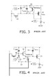
- FIGS. 3 and 4 show examples of pixel layout with optical feedback to provide ageing compensation.
- a photodiode 27 discharges the gate voltage stored on the capacitor 24 (C data ), causing the brightness to reduce.
- the display element 2 will no longer emit when the gate voltage on the drive transistor 22 (T drive ) reaches the threshold voltage, and the storage capacitor 24 will then stop discharging.
- the rate at which charge is leaked from the photodiode 27 is a function of the display element output, so that the photodiode 27 functions as a light-sensitive feedback device.
- the display element anode voltage reduces causing the discharge transistor 29 (T discharge ) to turn on, so that the remaining charge on the storage capacitor 24 is rapidly lost and the luminance is switched off.
- FIG. 4 shows a circuit which has been proposed by the applicant, and which has a constant light output and then switches off at a time dependent on the light output.
- the gate-source voltage for the drive transistor 22 is again held on a storage capacitor 24 (C store ). However, in this circuit, this capacitor 24 is charged to a fixed voltage from a charging line 32 , by means of a charging transistor 34 . Thus, the drive transistor 22 is driven to a constant level which is independent of the data input to the pixel when the display element is to be illuminated.
- the brightness is controlled by varying the duty cycle, in particular by varying the time when the drive transistor is turned off.
- the drive transistor 22 is turned off by means of a discharge transistor 36 which discharges the storage capacitor 24 .
- a discharge transistor 36 which discharges the storage capacitor 24 .
- the discharge transistor 36 is turned on when the gate voltage reaches a sufficient voltage.
- a photodiode 27 is illuminated by the display element 2 and again generates a photocurrent in dependence on the light output of the display element 2 .
- This photocurrent charges a discharge capacitor 40 (C data ), and at a certain point in time, the voltage across the capacitor 40 will reach the threshold voltage of the discharge transistor 36 and thereby switch it on. This time will depend on the charge originally stored on the capacitor 40 and on the photocurrent, which in turn depends on the light output of the display element.
- the discharge capacitor initially stores a data voltage, so that both the initial data and the optical feedback influence the duty cycle of the circuit.
- FIGS. 3 and 4 show p-type implementations, and there are also n-type implementations, for example for amorphous silicon transistors.
- the photodiode 52 is constructed outside the pixel apertures.
- the lateral illumination allows the NIP/PIN device to have its top window covered with metal, so that the passage of ambient light to the sensor can also be reduced.
- the efficiency of the NIP/PIN photodiode used in this manner will be good across all wavelengths, as absorption losses in the N and P layers of the device are no longer seen as light can enter through the side of the device.
- the light level will be lower than if the device were directly under the aperture so a large photodiode is preferred as shown in FIG. 5 . This removes the non-uniformity effects of very small devices.
- the laterally positioned photodiode can still receive light from above using reflecting paths.
- the arrangement of the invention is particularly suitable for display devices which emit light through the cathode (top emission) rather than devices that emit light through the anode (bottom emission). The reason for this will become apparent from the discussion below of the conventional pixel layouts for top and bottom emission.
- FIG. 6 shows the known basic bottom emission structure including the active matrix.
- the device comprises a substrate 60 over which the drive transistor semiconductor body 62 is deposited.
- a gate oxide dielectric layer 64 covers the semiconductor body, and a top gate electrode 66 is provided over the gate dielectric layer 64 .
- a first insulating layer 68 (typically silicon dioxide or silicon nitride) provides spacing between the gate electrode (which typically also forms row conductors) and the source and drain electrodes. These source and drain electrodes are defined by a metal layer 70 over the insulator layer 68 , and the electrodes connect to the semiconductor body through vias as shown.
- a second insulating layer 72 (again typically silicon dioxide or silicon nitride) provides spacing between the source and drain electrodes (which typically also form column conductors) and the LED anode.
- the LED anode 74 is provided over the second insulating layer 72 .
- this bottom anode needs to be at least partially transparent, and ITO is typically used.
- the EL material 76 is formed in a well over the anode, and is preferably deposited by printing. Separate sub-pixels are formed for the three primary colours, and a print dam 78 assists in the accurate printing of the different EL materials.
- the print dam 78 enables printing of separate pixels.
- This dam layer is generally made of an insulating polymer and has a height of several microns.
- a common cathode 80 is provided over the display, and this is reflective and at a common potential for all pixels (ground in FIG. 2 ).
- FIG. 7 shows the basic known top emission structure including the active matrix.
- the structure is essentially the same as in FIG. 6 , but the anode 74 a is reflective and the cathode 80 a is transmissive.
- the cathode may again be formed from ITO, but may have a thin metal, combination of several metals (e.g. Bg/Ag), or silicide coating between the ITO and polymer to control the barrier for electron injection. For example, this may be a thin 5 nm layer of Barium/20 nm layer of Silver. Protection and encapsulation layers 82 cover the display.
- a transparent cathode In a top-emission display, a transparent cathode is needed.
- the cathode does, however, have to be highly conductive, and at present highly conductive transparent metals are not readily available. Therefore the cathode of top-emission displays comprises a (semi-) transparent layer on top of the emissive pixel part and shunted with a lower resistance conducting (non-transparent) metal 79 . By placing this highly conductive metal 79 on top of the dam 78 as shown, there is no loss in pixel aperture.
- the anode metal can be a high work function metal, and it is known to provide a layer of ITO on top of a reflective metal to achieve a high work function into the LED stack.
- the anode electrode can also satisfy requirements relating to the physical properties of the electroluminescent materials, for example the wetting of the polymers.
- FIG. 8 shows the integration of an amorphous silicon PIN/NIP photo-diode 84 in a bottom emitting structure, in conventional manner.
- This type of photo-sensor is preferred as the amorphous silicon has high quantum efficiency for photo absorption.
- This type of photo-sensor is ideal for bottom emission as the gate metal which is used to form the bottom electrode 86 of the diode stack screens the photo-sensor from external light 87 .
- An open top aperture of the diode stack shown schematically in FIG. 8 , allows in light from the LED as shown by arrow 88 .
- the positioning of the sensor, beneath the anode layer is clearly not appropriate for top emission where the anode is a reflective and opaque metal. Furthermore, the diode can give rise to step coverage problems in the electroluminescent material layer, giving non-uniformity of pixel characteristics.
- FIG. 9 shows in more detail a first implementation of the invention for use in a top emission structure. Where the components in FIG. 9 correspond to those in FIGS. 6 and 7 , the same references are used and the description is not repeated.
- the photodiode 90 is positioned at the side of the EL material area of the display, and comprises an NIP/PIN stack for example of height approximately 1.5 ⁇ m.
- the photodiode is illuminated by light emitted from the side of the LED aperture as shown by arrow 92 .
- the diode stack is sandwiched between top and bottom electrodes 93 , 94 , and in the structure shown, the bottom electrode is formed from the source/drain metal layer 70 and the top electrode 93 is formed from the anode metal layer 74 a .
- the top electrode covers the top of the diode stack so that the device is illuminated laterally only.
- the top electrode 93 also shields the diode stack from illumination from one side as well as from above.
- FIG. 9 gives example layer thickness for the insulator layer 72 above the source/drain and for the anode metal. These heights allow vertical adjustment of the LED layer 76 with respect to the diode stack. A diode of 1.5 ⁇ m height is sufficient to gather light from the LED. Thinning the anode metal can enable the diode to gather more light as the LED will emit upwardly, so the more of the photodiode above the plane of the electroluminescent layer, the more light it will gather.
- a thick amorphous silicon photodiode presents no extra planarisation issues because the diode is not under the LED aperture.
- the layer 72 planarises the TFTs under the pixel aperture.
- the diode should be made as long as possible, preferably the same length as a dimension of the aperture, to gather as much light as possible. Its width can be limited to a few microns because the wall width is simply required to absorb red photons. This is also advantageous because the dam width is likely to be narrow in pixel designs at high resolution.
- the screening of the photodiode from external light is achieved by the top diode contact formed using the anode metal, as mentioned above. Even light entering the display at a very shallow angle will be refracted strongly towards the display normal (as the materials used have a high refractive index e.g. n>1.8) so that the top contact anode metal still blocks this light.
- the diode should also be screened from light from neighbouring pixels by making sure the metal anode making the top contact on the diode of acts as a light block as shown in FIG. 9 .
- FIG. 10 shows (more schematically) a modification in which a reflective path is defined between the display material 76 and the photodiode 90 . This enables the photodiode to collect light over an area rather than an edge, and allows more flexibility in the vertical positioning of the photodiode within the layer structure.
- FIG. 10 shows only the layers relevant to the modification, and is a partial representation of the device.
- the column metal 70 is used to reflect the downwardly directed light, rather than a reflective anode.
- the LED anode 74 is transparent and connects to the column metal layer 70 through a via, as shown.
- the photodiode 90 is now positioned out of the direct line of sight of the LED layer 76 , and it is placed at the level of the gate metal 62 instead of at the column metal level as in FIG. 9 . Direct light collected may cause non-uniformity due to sensitivity to the precise vertical position, and the embodiment of FIG. 10 reduces this sensitivity.
- the reflector under the pixel should ideally be as deep as possible under the ITO anode 74 , and should also extend laterally beyond the ITO anode 74 as shown in FIG. 10 , to increase the angle of collection.
- This reflector 102 directs light to the top of the photodiode but also acts as a light shield for ambient light.
- FIG. 11 shows a variation to FIG. 10 , in which the top mirror 110 is added at the level of the ITO anode 74 . Again, the first reflection is provided by the column metal layer 70 .
- FIG. 11 also shows more clearly the photodiode 90 formed on the gate metal layer 62 , and also shows the TFT semiconductor layer 66 and gate dielectric layer 64 .
- the processing stage for connecting the ITO anode 74 to the column metal layer using vias can also be used to form an angled mirror 110 for higher efficiency, as shown in FIG. 11 .
- the other levels under the LED (such as the gate metal 62 and semiconductor layers 66 ) can also be used to adjust the height of the pixel with respect to the photodiode, as necessary to control light angles.
- the LED and top layers, as well as the printing dam, are not shown in FIG. 11 .
- FIG. 12 shows a further modification in which the height difference between the two mirrors is further increased to improve light collection efficiency.
- the dam polymer is again used to define the mirror 102 at the higher level, but the gate metal layer 62 rather than the column metal is used to define the bottom mirror.
- the top mirror metal can also be etched under the dam 78 to provide an angled profile, and this can reduce any pixel to pixel leakage.
- the semiconductor layer 66 can also be removed from under the gate metal portion forming the bottom reflector to give increased separation, or left in place as shown. This semiconductor layer has high surface roughness, which propagates up through to the gate metal layer, and this roughness may enhance light scattering to the shallow angles.
- FIG. 12 With the gate metal used as a reflector, gives giving maximum ITO layer 74 to reflector separation. Having the top reflector as high up the structure as possible also enables light to be collected over a wider range of angles.
- FIG. 13 shows for completeness a top view of a triplet of three active matrix LED pixels 50 (R, G, B), the dams 78 and the photo-sensors 90 at one side of the pixel underneath the dam.
- FIG. 14 shows a cross section of the combination of the pixel and dam.
- the diode it is important to reduce the leakage current. This can be provided for by placing isolating spacers 130 at both sides of the diode to decrease current leakage at the sidewalls.
- FIG. 14 also shows a further method of reducing optical crosstalk, in which the cathode shunt metal 79 on top of the dam is asymmetric. At the right side of the dam, the metal 79 shields the photo-sensor from light emitted by the neighbouring pixel, and this can be used in combination with the use of the top electrode as discussed above (for example as shown by contact 132 ).
- the area of the photodiode that receives light is given by the area of the sidewall facing the LED layer. Since the height of the diode stack may be 1.5 ⁇ m or less, the area may be very small. As mentioned above, although the height of the diodes is preferably relatively low, the width can be as large as the pixel length, as shown in FIG. 13 .
- the length of the exposed side wall of the diode stack can be increased further as shown in FIG. 15 .
- most of the circumference of the pixel active area is used to illuminate a photodiode, excluding one edge (the left edge in FIG. 15 ). At this edge, the photodiode of the neighbouring pixel is positioned.
- This configuration increases further the amount of light sensed by the photo diode.
- the metal dam can in this case be used both as the gate of the amorphous silicon photo TFT and the shunt 79 between cathodes. Light emitted at a slight angle to the substrate may again be reflected by the inside of the metal 79 towards the photo TFT, increasing the size of the photocurrent.
- the embodiment of FIG. 15 uses a dam formed from an insulating transparent material covered by the shunt metal 79 .
- a low temperature polysilicon photo TFT can also be used as the photosensitive device, with a resulting geometry similar to FIG. 16 .
- Display devices of the invention will find particular application as flat panel displays in mobile applications (Phone, PDA, digital camera), in (laptop) monitors, and in televisions.
- the invention also provides a solution to avoid ambient light sensitivity in trans-emissive displays, for example for use in window or head mounted displays. In the case of a trans-emissive display, daylight from the other side can be shielded for example by the power supply line.
- Amorphous silicon, polysilicon, microcrystalline silicon or other semiconductor transistor technologies may be employed.
- the invention can be applied to any pixel circuit in which a photosensitive device is used as a feedback element for each pixel.
- the invention provides particular advantages for top emission device structures.
- the invention can also be used to improve light collection efficiency and remove step coverage problems in bottom emission display structures.
Landscapes
- Engineering & Computer Science (AREA)
- Physics & Mathematics (AREA)
- Microelectronics & Electronic Packaging (AREA)
- Computer Hardware Design (AREA)
- General Physics & Mathematics (AREA)
- Power Engineering (AREA)
- Theoretical Computer Science (AREA)
- Condensed Matter Physics & Semiconductors (AREA)
- Geometry (AREA)
- Optics & Photonics (AREA)
- Electroluminescent Light Sources (AREA)
- Devices For Indicating Variable Information By Combining Individual Elements (AREA)
- Control Of Indicators Other Than Cathode Ray Tubes (AREA)
Abstract
Description
Claims (21)
Applications Claiming Priority (3)
| Application Number | Priority Date | Filing Date | Title |
|---|---|---|---|
| GB0406107.3 | 2004-03-17 | ||
| GBGB0406107.3A GB0406107D0 (en) | 2004-03-17 | 2004-03-17 | Electroluminescent display devices |
| PCT/IB2005/050768 WO2005091262A1 (en) | 2004-03-17 | 2005-03-02 | Electroluminescent display devices |
Publications (2)
| Publication Number | Publication Date |
|---|---|
| US20070241998A1 US20070241998A1 (en) | 2007-10-18 |
| US8310413B2 true US8310413B2 (en) | 2012-11-13 |
Family
ID=32117952
Family Applications (1)
| Application Number | Title | Priority Date | Filing Date |
|---|---|---|---|
| US10/598,822 Active 2027-10-25 US8310413B2 (en) | 2004-03-17 | 2005-03-02 | Electroluminescent display devices |
Country Status (8)
| Country | Link |
|---|---|
| US (1) | US8310413B2 (en) |
| EP (1) | EP1728234A1 (en) |
| JP (1) | JP2007529775A (en) |
| KR (1) | KR20070004718A (en) |
| CN (1) | CN1934605A (en) |
| GB (1) | GB0406107D0 (en) |
| TW (1) | TW200603672A (en) |
| WO (1) | WO2005091262A1 (en) |
Cited By (18)
| Publication number | Priority date | Publication date | Assignee | Title |
|---|---|---|---|---|
| DE102012222461A1 (en) * | 2012-12-06 | 2014-06-12 | Osram Opto Semiconductors Gmbh | Organic optoelectronic component |
| US8994625B2 (en) * | 2004-12-15 | 2015-03-31 | Ignis Innovation Inc. | Method and system for programming, calibrating and driving a light emitting device display |
| US9739938B2 (en) | 2015-12-09 | 2017-08-22 | Elenion Technologies, Llc | Shielded photonic integrated circuit |
| US10325537B2 (en) | 2011-05-20 | 2019-06-18 | Ignis Innovation Inc. | System and methods for extraction of threshold and mobility parameters in AMOLED displays |
| US10339860B2 (en) | 2015-08-07 | 2019-07-02 | Ignis Innovation, Inc. | Systems and methods of pixel calibration based on improved reference values |
| US10380944B2 (en) | 2011-11-29 | 2019-08-13 | Ignis Innovation Inc. | Structural and low-frequency non-uniformity compensation |
| US10615231B2 (en) | 2017-09-20 | 2020-04-07 | Boe Technology Group Co., Ltd. | Organic light emitting diode substrate, method for manufacturing the same, and display panel |
| US20200127220A1 (en) * | 2018-10-23 | 2020-04-23 | Samsung Display Co., Ltd. | Display apparatus and mask for manufacturing the same |
| US10699624B2 (en) | 2004-12-15 | 2020-06-30 | Ignis Innovation Inc. | Method and system for programming, calibrating and/or compensating, and driving an LED display |
| US11133367B2 (en) | 2018-05-21 | 2021-09-28 | Boe Technology Group Co., Ltd. | Thin film transistor and fabricating method thereof, array substrate and display device |
| US11200839B2 (en) | 2010-02-04 | 2021-12-14 | Ignis Innovation Inc. | System and methods for extracting correlation curves for an organic light emitting device |
| US11257425B2 (en) | 2018-11-30 | 2022-02-22 | Boe Technology Group Co., Ltd. | Display panel and method for manufacturing the same, pixel light emitting compensation method and display apparatus |
| US11487859B2 (en) | 2020-07-31 | 2022-11-01 | Apple Inc. | Behind display polarized optical transceiver |
| US11527582B1 (en) | 2019-09-24 | 2022-12-13 | Apple Inc. | Display stack with integrated photodetectors |
| US11611058B2 (en) | 2019-09-24 | 2023-03-21 | Apple Inc. | Devices and systems for under display image sensor |
| US11839133B2 (en) | 2021-03-12 | 2023-12-05 | Apple Inc. | Organic photodetectors for in-cell optical sensing |
| US12063802B2 (en) | 2019-10-17 | 2024-08-13 | Semiconductor Energy Laboratory Co., Ltd. | Display apparatus, display module, and electronic device |
| US12096670B2 (en) | 2019-07-17 | 2024-09-17 | Semiconductor Energy Laboratory Co., Ltd. | Display apparatus, display module, and electronic device |
Families Citing this family (49)
| Publication number | Priority date | Publication date | Assignee | Title |
|---|---|---|---|---|
| JP4822437B2 (en) * | 2006-01-07 | 2011-11-24 | 株式会社半導体エネルギー研究所 | Display device and manufacturing method thereof |
| KR101238721B1 (en) * | 2006-01-07 | 2013-03-06 | 가부시키가이샤 한도오따이 에네루기 켄큐쇼 | Display device and manufacturing method of the same |
| US20070236428A1 (en) * | 2006-03-28 | 2007-10-11 | Toppoly Optoelectronics Corp. | Organic electroluminescent device and fabrication methods thereof |
| US20070236429A1 (en) * | 2006-03-28 | 2007-10-11 | Toppoly Optoelectronics Corp. | Organic electroluminescent device and fabrication methods thereof |
| KR100759681B1 (en) * | 2006-03-29 | 2007-09-17 | 삼성에스디아이 주식회사 | Organic light emitting diode |
| KR100762682B1 (en) * | 2006-05-03 | 2007-10-01 | 삼성에스디아이 주식회사 | Organic light emitting display device and method for fabricating the same |
| GB2439584A (en) * | 2006-06-30 | 2008-01-02 | Cambridge Display Tech Ltd | Active Matrix Organic Electro-Optic Devices |
| JP4356026B2 (en) | 2006-10-10 | 2009-11-04 | ソニー株式会社 | Display device, light receiving method, and information processing device |
| US7932879B2 (en) * | 2007-05-08 | 2011-04-26 | Sony Ericsson Mobile Communications Ab | Controlling electroluminescent panels in response to cumulative utilization |
| JP4840304B2 (en) * | 2007-09-12 | 2011-12-21 | カシオ計算機株式会社 | Light emitting device and image forming apparatus having the same |
| TWI371223B (en) * | 2008-02-20 | 2012-08-21 | Chimei Innolux Corp | Organic light emitting display device and fabrications thereof and electronic device |
| US9570004B1 (en) * | 2008-03-16 | 2017-02-14 | Nongqiang Fan | Method of driving pixel element in active matrix display |
| JP2009238833A (en) * | 2008-03-26 | 2009-10-15 | Sony Corp | Image display device |
| JP5195071B2 (en) * | 2008-06-25 | 2013-05-08 | セイコーエプソン株式会社 | LIGHT EMITTING DEVICE AND ELECTRONIC DEVICE |
| KR101534006B1 (en) | 2008-07-29 | 2015-07-06 | 삼성디스플레이 주식회사 | Organic light emitting device |
| JP5217859B2 (en) * | 2008-09-30 | 2013-06-19 | カシオ計算機株式会社 | Light emitting device, light emitting device manufacturing method, and image forming apparatus |
| JP4688229B2 (en) * | 2008-10-03 | 2011-05-25 | 東芝モバイルディスプレイ株式会社 | Display device |
| ES2386657B1 (en) * | 2011-01-27 | 2013-07-05 | Senia Technologies, S.L. | LED'S VIDEO SCREEN. |
| US9129578B2 (en) * | 2012-09-28 | 2015-09-08 | Innocom Technology (Shenzhen) Co., Ltd. | Shift register circuit and display device using the same |
| DE102012220045A1 (en) * | 2012-11-02 | 2014-05-08 | Osram Opto Semiconductors Gmbh | Method for operating an organic optoelectronic component |
| DE102012220053A1 (en) * | 2012-11-02 | 2014-05-22 | Osram Opto Semiconductors Gmbh | METHOD FOR OPERATING AN ORGANIC OPTOELECTRONIC COMPONENT |
| CN103268921B (en) * | 2012-12-31 | 2016-04-20 | 上海天马微电子有限公司 | method for manufacturing WOLED, WOLED and display device |
| JP2014194517A (en) * | 2013-02-27 | 2014-10-09 | Sony Corp | Display device, manufacturing method of the display device, drive method of the display device and electronic apparatus |
| CN104733644A (en) * | 2013-12-24 | 2015-06-24 | 昆山国显光电有限公司 | Organic light-emitting display device and manufacturing method thereof |
| US10910350B2 (en) * | 2014-05-24 | 2021-02-02 | Hiphoton Co., Ltd. | Structure of a semiconductor array |
| KR102357505B1 (en) * | 2014-07-25 | 2022-02-04 | 삼성디스플레이 주식회사 | Display device |
| CN105449107B (en) * | 2014-08-15 | 2018-08-10 | 北京维信诺科技有限公司 | A kind of top-illuminating OLED device and preparation method thereof |
| CN104659072B (en) * | 2015-03-16 | 2017-07-28 | 京东方科技集团股份有限公司 | Array base palte and array substrate manufacturing method |
| KR20160117817A (en) * | 2015-03-31 | 2016-10-11 | 삼성디스플레이 주식회사 | Pixel and display device using the same |
| JP2017026973A (en) | 2015-07-28 | 2017-02-02 | ソニー株式会社 | Display panel, display device and electronic apparatus |
| JP2017168397A (en) * | 2016-03-18 | 2017-09-21 | 株式会社ジャパンディスプレイ | Display device |
| US9961178B2 (en) | 2016-03-24 | 2018-05-01 | Motorola Mobility Llc | Embedded active matrix organic light emitting diode (AMOLED) fingerprint sensor |
| US20170289805A1 (en) * | 2016-03-30 | 2017-10-05 | Motorola Mobility Llc | Embedded active matrix organic light emitting diode (amoled) fingerprint sensor and self-compensating amoled |
| US10431164B2 (en) * | 2016-06-16 | 2019-10-01 | Semiconductor Energy Laboratory Co., Ltd. | Display device, display module, and electronic device |
| CN106229330B (en) * | 2016-08-24 | 2019-04-02 | 昆山工研院新型平板显示技术中心有限公司 | OLED display panel |
| CN107331793B (en) * | 2017-07-25 | 2019-06-14 | 南京迈智芯微光电科技有限公司 | A kind of silicon-based organic light-emitting device bottom electrode structural and its manufacturing method |
| JP2019160621A (en) * | 2018-03-14 | 2019-09-19 | パイオニア株式会社 | Optical device |
| CN108615826B (en) * | 2018-05-04 | 2019-10-25 | 京东方科技集团股份有限公司 | A kind of organic light-emitting diode display substrate and preparation method thereof, display device |
| CN108878503B (en) * | 2018-07-26 | 2021-01-05 | 京东方科技集团股份有限公司 | OLED display substrate, manufacturing method thereof, OLED display panel and display device |
| CN109166865B (en) * | 2018-08-08 | 2020-11-10 | 深圳市华星光电技术有限公司 | Array substrate, manufacturing method thereof and display panel |
| CN110970466B (en) * | 2018-09-28 | 2023-12-26 | 乐金显示有限公司 | Display apparatus including light receiving device |
| CN110164384B (en) * | 2018-09-29 | 2022-06-10 | 京东方科技集团股份有限公司 | Brightness compensation method and device |
| KR102687203B1 (en) * | 2018-10-01 | 2024-07-19 | 엘지디스플레이 주식회사 | Display apparatus including light rpceving pixel area |
| EP3874546B1 (en) * | 2018-11-01 | 2023-08-02 | Boe Technology Group Co., Ltd. | Light emitting diode and fabrication method thereof, array substrate and display panel |
| CN109638047B (en) * | 2018-12-13 | 2020-12-22 | 京东方科技集团股份有限公司 | Display panel, manufacturing method thereof and method for driving display panel |
| US20210050385A1 (en) * | 2019-08-13 | 2021-02-18 | Apple Inc. | Photodetectors Integrated into Thin-Film Transistor Backplanes |
| CN111653602B (en) * | 2020-06-17 | 2023-04-07 | 京东方科技集团股份有限公司 | Organic electroluminescent display panel, manufacturing method thereof and display device |
| CN112201684B (en) * | 2020-10-30 | 2024-04-19 | 京东方科技集团股份有限公司 | Display panel, display device and preparation method of display panel |
| WO2024190878A1 (en) * | 2023-03-16 | 2024-09-19 | Kepler株式会社 | Display with incorporated two-dimensional photosensor and method for manufacturing display with built-in two-dimensional photosensor |
Citations (13)
| Publication number | Priority date | Publication date | Assignee | Title |
|---|---|---|---|---|
| EP0717446A2 (en) | 1994-12-14 | 1996-06-19 | Eastman Kodak Company | TFT-EL display panel using organic electroluminiscent media |
| US5751261A (en) * | 1990-12-31 | 1998-05-12 | Kopin Corporation | Control system for display panels |
| WO2001020591A1 (en) | 1999-09-11 | 2001-03-22 | Koninklijke Philips Electronics N.V. | Active matrix electroluminescent display device |
| EP1096466A1 (en) | 1999-10-27 | 2001-05-02 | Agilent Technologies Inc. | Active matrix electroluminescent display |
| US20010026125A1 (en) * | 2000-03-27 | 2001-10-04 | Shunpei Yamazaki | Light emitting device and a method of manufacturing the same |
| US6320325B1 (en) | 2000-11-06 | 2001-11-20 | Eastman Kodak Company | Emissive display with luminance feedback from a representative pixel |
| US20020027229A1 (en) * | 2000-06-12 | 2002-03-07 | Semiconductor Energy Laboratory Co., Ltd. | Light emitting module and method of driving the same, and optical sensor |
| US20020079512A1 (en) * | 2000-12-12 | 2002-06-27 | Shunpei Yamazaki | Information device |
| US6424326B2 (en) * | 2000-01-11 | 2002-07-23 | Semiconductor Energy Laboratory Co., Ltd. | Semiconductor display device having a display portion and a sensor portion |
| US20030047736A1 (en) * | 2001-02-27 | 2003-03-13 | Nec Corporation | Light emitting device and light emitting system |
| US20040031965A1 (en) * | 2002-08-16 | 2004-02-19 | Forrest Stephen R. | Organic photonic integrated circuit using an organic photodetector and a transparent organic light emitting device |
| US6774578B2 (en) * | 2000-09-19 | 2004-08-10 | Semiconductor Energy Laboratory Co., Ltd. | Self light emitting device and method of driving thereof |
| US20050253790A1 (en) * | 2002-07-10 | 2005-11-17 | Sharp Kabushiki Kaisha | Display apparatus and image reading/displaying system incorporating the same |
-
2004
- 2004-03-17 GB GBGB0406107.3A patent/GB0406107D0/en not_active Ceased
-
2005
- 2005-03-02 JP JP2007503456A patent/JP2007529775A/en not_active Withdrawn
- 2005-03-02 CN CNA2005800084383A patent/CN1934605A/en active Pending
- 2005-03-02 WO PCT/IB2005/050768 patent/WO2005091262A1/en not_active Application Discontinuation
- 2005-03-02 EP EP05708906A patent/EP1728234A1/en not_active Ceased
- 2005-03-02 KR KR1020067018786A patent/KR20070004718A/en not_active Application Discontinuation
- 2005-03-02 US US10/598,822 patent/US8310413B2/en active Active
- 2005-03-14 TW TW094107625A patent/TW200603672A/en unknown
Patent Citations (17)
| Publication number | Priority date | Publication date | Assignee | Title |
|---|---|---|---|---|
| US5751261A (en) * | 1990-12-31 | 1998-05-12 | Kopin Corporation | Control system for display panels |
| EP0717446A2 (en) | 1994-12-14 | 1996-06-19 | Eastman Kodak Company | TFT-EL display panel using organic electroluminiscent media |
| WO2001020591A1 (en) | 1999-09-11 | 2001-03-22 | Koninklijke Philips Electronics N.V. | Active matrix electroluminescent display device |
| EP1096466A1 (en) | 1999-10-27 | 2001-05-02 | Agilent Technologies Inc. | Active matrix electroluminescent display |
| US6424326B2 (en) * | 2000-01-11 | 2002-07-23 | Semiconductor Energy Laboratory Co., Ltd. | Semiconductor display device having a display portion and a sensor portion |
| US20020180672A1 (en) * | 2000-01-11 | 2002-12-05 | Semiconductor Energy Laboratory Co., Ltd., A Japan Corporation | Semiconductor display device |
| US20010026125A1 (en) * | 2000-03-27 | 2001-10-04 | Shunpei Yamazaki | Light emitting device and a method of manufacturing the same |
| US20020027229A1 (en) * | 2000-06-12 | 2002-03-07 | Semiconductor Energy Laboratory Co., Ltd. | Light emitting module and method of driving the same, and optical sensor |
| US20060132401A1 (en) * | 2000-06-12 | 2006-06-22 | Semiconductor Energy Laboratory Co., Ltd. | Light emitting module and method of driving the same, and optical sensor |
| US7068246B2 (en) * | 2000-06-12 | 2006-06-27 | Semiconductor Energy Laboratory Co., Ltd. | Light emitting module and method of driving the same, and optical sensor |
| US6774578B2 (en) * | 2000-09-19 | 2004-08-10 | Semiconductor Energy Laboratory Co., Ltd. | Self light emitting device and method of driving thereof |
| US20080170007A1 (en) * | 2000-09-19 | 2008-07-17 | Semiconductor Energy Laboratory Co., Ltd. | Self Light Emitting Device and Method of Driving Thereof |
| US6320325B1 (en) | 2000-11-06 | 2001-11-20 | Eastman Kodak Company | Emissive display with luminance feedback from a representative pixel |
| US20020079512A1 (en) * | 2000-12-12 | 2002-06-27 | Shunpei Yamazaki | Information device |
| US20030047736A1 (en) * | 2001-02-27 | 2003-03-13 | Nec Corporation | Light emitting device and light emitting system |
| US20050253790A1 (en) * | 2002-07-10 | 2005-11-17 | Sharp Kabushiki Kaisha | Display apparatus and image reading/displaying system incorporating the same |
| US20040031965A1 (en) * | 2002-08-16 | 2004-02-19 | Forrest Stephen R. | Organic photonic integrated circuit using an organic photodetector and a transparent organic light emitting device |
Non-Patent Citations (2)
| Title |
|---|
| ISR: PCT/IB05/050768. |
| Written Opinion: PCT/IB05/050768. |
Cited By (23)
| Publication number | Priority date | Publication date | Assignee | Title |
|---|---|---|---|---|
| US8994625B2 (en) * | 2004-12-15 | 2015-03-31 | Ignis Innovation Inc. | Method and system for programming, calibrating and driving a light emitting device display |
| US10699624B2 (en) | 2004-12-15 | 2020-06-30 | Ignis Innovation Inc. | Method and system for programming, calibrating and/or compensating, and driving an LED display |
| US11200839B2 (en) | 2010-02-04 | 2021-12-14 | Ignis Innovation Inc. | System and methods for extracting correlation curves for an organic light emitting device |
| US10325537B2 (en) | 2011-05-20 | 2019-06-18 | Ignis Innovation Inc. | System and methods for extraction of threshold and mobility parameters in AMOLED displays |
| US10380944B2 (en) | 2011-11-29 | 2019-08-13 | Ignis Innovation Inc. | Structural and low-frequency non-uniformity compensation |
| DE102012222461A1 (en) * | 2012-12-06 | 2014-06-12 | Osram Opto Semiconductors Gmbh | Organic optoelectronic component |
| US9299748B2 (en) | 2012-12-06 | 2016-03-29 | Osram Oled Gmbh | Organic optoelectronic component |
| US10339860B2 (en) | 2015-08-07 | 2019-07-02 | Ignis Innovation, Inc. | Systems and methods of pixel calibration based on improved reference values |
| US9739938B2 (en) | 2015-12-09 | 2017-08-22 | Elenion Technologies, Llc | Shielded photonic integrated circuit |
| US10444451B2 (en) | 2015-12-09 | 2019-10-15 | Elenion Technologies, Llc | Shielded photonic integrated circuit |
| US10209465B2 (en) | 2015-12-09 | 2019-02-19 | Elenion Technologies, Llc | Shielded photonic integrated circuit |
| US10615231B2 (en) | 2017-09-20 | 2020-04-07 | Boe Technology Group Co., Ltd. | Organic light emitting diode substrate, method for manufacturing the same, and display panel |
| US11133367B2 (en) | 2018-05-21 | 2021-09-28 | Boe Technology Group Co., Ltd. | Thin film transistor and fabricating method thereof, array substrate and display device |
| US20200127220A1 (en) * | 2018-10-23 | 2020-04-23 | Samsung Display Co., Ltd. | Display apparatus and mask for manufacturing the same |
| US12075640B2 (en) * | 2018-10-23 | 2024-08-27 | Samsung Display Co., Ltd. | Display apparatus and mask for manufacturing the same |
| US11257425B2 (en) | 2018-11-30 | 2022-02-22 | Boe Technology Group Co., Ltd. | Display panel and method for manufacturing the same, pixel light emitting compensation method and display apparatus |
| US12096670B2 (en) | 2019-07-17 | 2024-09-17 | Semiconductor Energy Laboratory Co., Ltd. | Display apparatus, display module, and electronic device |
| US11527582B1 (en) | 2019-09-24 | 2022-12-13 | Apple Inc. | Display stack with integrated photodetectors |
| US11611058B2 (en) | 2019-09-24 | 2023-03-21 | Apple Inc. | Devices and systems for under display image sensor |
| US12016237B2 (en) | 2019-09-24 | 2024-06-18 | Apple Inc. | Display stack with integrated photodetectors |
| US12063802B2 (en) | 2019-10-17 | 2024-08-13 | Semiconductor Energy Laboratory Co., Ltd. | Display apparatus, display module, and electronic device |
| US11487859B2 (en) | 2020-07-31 | 2022-11-01 | Apple Inc. | Behind display polarized optical transceiver |
| US11839133B2 (en) | 2021-03-12 | 2023-12-05 | Apple Inc. | Organic photodetectors for in-cell optical sensing |
Also Published As
| Publication number | Publication date |
|---|---|
| WO2005091262A1 (en) | 2005-09-29 |
| US20070241998A1 (en) | 2007-10-18 |
| TW200603672A (en) | 2006-01-16 |
| GB0406107D0 (en) | 2004-04-21 |
| JP2007529775A (en) | 2007-10-25 |
| CN1934605A (en) | 2007-03-21 |
| KR20070004718A (en) | 2007-01-09 |
| EP1728234A1 (en) | 2006-12-06 |
Similar Documents
| Publication | Publication Date | Title |
|---|---|---|
| US8310413B2 (en) | Electroluminescent display devices | |
| US7859189B2 (en) | Electroluminescent display having a drive transistor controlled by a light sensitive device and a light blocking structure to prevent cross talk | |
| US20070205420A1 (en) | Electroluminescent display devices | |
| CN108831912B (en) | OLED array substrate, method for manufacturing OLED array substrate, OLED pixel circuit and display device | |
| CN107464529B (en) | Display base plate and preparation method thereof, display panel and its driving method | |
| US7242145B2 (en) | Color electroluminescent display devices | |
| US6489631B2 (en) | Light-emitting matrix array display devices with light sensing elements | |
| US6738031B2 (en) | Matrix array display devices with light sensing elements and associated storage capacitors | |
| US7602387B2 (en) | Electroluminescent display devices | |
| US20040257352A1 (en) | Method and apparatus for controlling | |
| CN111599825B (en) | Display substrate, display panel and manufacturing method of display substrate | |
| WO2001099190A1 (en) | Matrix array display devices with light sensing elements | |
| US20070236429A1 (en) | Organic electroluminescent device and fabrication methods thereof | |
| JP2001085160A (en) | Light emitting element with function of correcting light emission output | |
| EP1837912A1 (en) | Organic electroluminescent device and fabrication methods thereof | |
| US20230247880A1 (en) | Electro-optical device and electronic apparatus | |
| EP4161238A1 (en) | Display device |
Legal Events
| Date | Code | Title | Description |
|---|---|---|---|
| AS | Assignment |
Owner name: KONINKLIJKE PHILIPS ELECTRONICS N V, NETHERLANDS Free format text: ASSIGNMENT OF ASSIGNORS INTEREST;ASSIGNORS:FISH, DAVID A.;YOUNG, NIGEL D.;LIFKA, HERBERT;AND OTHERS;REEL/FRAME:018236/0446 Effective date: 20060801 |
|
| STCF | Information on status: patent grant |
Free format text: PATENTED CASE |
|
| FPAY | Fee payment |
Year of fee payment: 4 |
|
| AS | Assignment |
Owner name: KONINKLIJKE PHILIPS ELECTRONICS N.V., NETHERLANDS Free format text: CHANGE OF ADDRESS;ASSIGNOR:KONINKLIJKE PHILIPS ELECTRONICS N.V.;REEL/FRAME:046703/0202 Effective date: 20091201 Owner name: KONINKLIJKE PHILIPS N.V., NETHERLANDS Free format text: CHANGE OF NAME;ASSIGNOR:KONINKLIJKE PHILIPS ELECTRONICS N.V.;REEL/FRAME:047407/0258 Effective date: 20130515 |
|
| AS | Assignment |
Owner name: BEIJING XIAOMI MOBILE SOFTWARE CO., LTD., CHINA Free format text: ASSIGNMENT OF ASSIGNORS INTEREST;ASSIGNOR:KONINKLIJKE PHILIPS N.V.;REEL/FRAME:046633/0913 Effective date: 20180309 |
|
| MAFP | Maintenance fee payment |
Free format text: PAYMENT OF MAINTENANCE FEE, 8TH YEAR, LARGE ENTITY (ORIGINAL EVENT CODE: M1552); ENTITY STATUS OF PATENT OWNER: LARGE ENTITY Year of fee payment: 8 |
|
| MAFP | Maintenance fee payment |
Free format text: PAYMENT OF MAINTENANCE FEE, 12TH YEAR, LARGE ENTITY (ORIGINAL EVENT CODE: M1553); ENTITY STATUS OF PATENT OWNER: LARGE ENTITY Year of fee payment: 12 |