JP2014194517A - Display device, manufacturing method of the display device, drive method of the display device and electronic apparatus - Google Patents
Display device, manufacturing method of the display device, drive method of the display device and electronic apparatus Download PDFInfo
- Publication number
- JP2014194517A JP2014194517A JP2013159320A JP2013159320A JP2014194517A JP 2014194517 A JP2014194517 A JP 2014194517A JP 2013159320 A JP2013159320 A JP 2013159320A JP 2013159320 A JP2013159320 A JP 2013159320A JP 2014194517 A JP2014194517 A JP 2014194517A
- Authority
- JP
- Japan
- Prior art keywords
- display device
- light
- light emitting
- light receiving
- substrate
- Prior art date
- Legal status (The legal status is an assumption and is not a legal conclusion. Google has not performed a legal analysis and makes no representation as to the accuracy of the status listed.)
- Pending
Links
- 238000000034 method Methods 0.000 title claims description 51
- 238000004519 manufacturing process Methods 0.000 title claims description 14
- 239000000758 substrate Substances 0.000 claims abstract description 112
- 238000012937 correction Methods 0.000 claims description 36
- 229910052751 metal Inorganic materials 0.000 claims description 16
- 239000002184 metal Substances 0.000 claims description 16
- 238000006243 chemical reaction Methods 0.000 claims description 12
- XUIMIQQOPSSXEZ-UHFFFAOYSA-N Silicon Chemical compound [Si] XUIMIQQOPSSXEZ-UHFFFAOYSA-N 0.000 claims description 10
- 229910052710 silicon Inorganic materials 0.000 claims description 10
- 239000010703 silicon Substances 0.000 claims description 10
- 239000010949 copper Substances 0.000 claims description 7
- RYGMFSIKBFXOCR-UHFFFAOYSA-N Copper Chemical compound [Cu] RYGMFSIKBFXOCR-UHFFFAOYSA-N 0.000 claims description 5
- 229910052802 copper Inorganic materials 0.000 claims description 5
- 230000035945 sensitivity Effects 0.000 abstract description 4
- 239000010410 layer Substances 0.000 description 134
- 239000010408 film Substances 0.000 description 52
- 239000000463 material Substances 0.000 description 23
- 238000002955 isolation Methods 0.000 description 17
- 238000005516 engineering process Methods 0.000 description 14
- 238000012986 modification Methods 0.000 description 12
- 230000004048 modification Effects 0.000 description 12
- 239000012044 organic layer Substances 0.000 description 12
- 238000002347 injection Methods 0.000 description 11
- 239000007924 injection Substances 0.000 description 11
- 229910052782 aluminium Inorganic materials 0.000 description 10
- XAGFODPZIPBFFR-UHFFFAOYSA-N aluminium Chemical compound [Al] XAGFODPZIPBFFR-UHFFFAOYSA-N 0.000 description 10
- 238000010586 diagram Methods 0.000 description 9
- 230000015572 biosynthetic process Effects 0.000 description 8
- 125000004432 carbon atom Chemical group C* 0.000 description 7
- 239000011241 protective layer Substances 0.000 description 7
- 239000010936 titanium Substances 0.000 description 7
- WFKWXMTUELFFGS-UHFFFAOYSA-N tungsten Chemical compound [W] WFKWXMTUELFFGS-UHFFFAOYSA-N 0.000 description 7
- 229910052721 tungsten Inorganic materials 0.000 description 7
- 239000010937 tungsten Substances 0.000 description 7
- PXHVJJICTQNCMI-UHFFFAOYSA-N Nickel Chemical compound [Ni] PXHVJJICTQNCMI-UHFFFAOYSA-N 0.000 description 6
- 229910052581 Si3N4 Inorganic materials 0.000 description 6
- 239000003990 capacitor Substances 0.000 description 6
- 230000000694 effects Effects 0.000 description 6
- BASFCYQUMIYNBI-UHFFFAOYSA-N platinum Chemical compound [Pt] BASFCYQUMIYNBI-UHFFFAOYSA-N 0.000 description 6
- HQVNEWCFYHHQES-UHFFFAOYSA-N silicon nitride Chemical compound N12[Si]34N5[Si]62N3[Si]51N64 HQVNEWCFYHHQES-UHFFFAOYSA-N 0.000 description 6
- VYPSYNLAJGMNEJ-UHFFFAOYSA-N Silicium dioxide Chemical compound O=[Si]=O VYPSYNLAJGMNEJ-UHFFFAOYSA-N 0.000 description 5
- BQCADISMDOOEFD-UHFFFAOYSA-N Silver Chemical compound [Ag] BQCADISMDOOEFD-UHFFFAOYSA-N 0.000 description 5
- RTAQQCXQSZGOHL-UHFFFAOYSA-N Titanium Chemical compound [Ti] RTAQQCXQSZGOHL-UHFFFAOYSA-N 0.000 description 5
- NRTOMJZYCJJWKI-UHFFFAOYSA-N Titanium nitride Chemical compound [Ti]#N NRTOMJZYCJJWKI-UHFFFAOYSA-N 0.000 description 5
- XLOMVQKBTHCTTD-UHFFFAOYSA-N Zinc monoxide Chemical compound [Zn]=O XLOMVQKBTHCTTD-UHFFFAOYSA-N 0.000 description 5
- 229910045601 alloy Inorganic materials 0.000 description 5
- 239000000956 alloy Substances 0.000 description 5
- 238000007667 floating Methods 0.000 description 5
- 230000000149 penetrating effect Effects 0.000 description 5
- 239000004332 silver Substances 0.000 description 5
- 239000000126 substance Substances 0.000 description 5
- 229910052719 titanium Inorganic materials 0.000 description 5
- 239000004020 conductor Substances 0.000 description 4
- 230000005525 hole transport Effects 0.000 description 4
- 239000011777 magnesium Substances 0.000 description 4
- 238000005498 polishing Methods 0.000 description 4
- 229910052814 silicon oxide Inorganic materials 0.000 description 4
- 229910052709 silver Inorganic materials 0.000 description 4
- 238000004544 sputter deposition Methods 0.000 description 4
- UHXOHPVVEHBKKT-UHFFFAOYSA-N 1-(2,2-diphenylethenyl)-4-[4-(2,2-diphenylethenyl)phenyl]benzene Chemical compound C=1C=C(C=2C=CC(C=C(C=3C=CC=CC=3)C=3C=CC=CC=3)=CC=2)C=CC=1C=C(C=1C=CC=CC=1)C1=CC=CC=C1 UHXOHPVVEHBKKT-UHFFFAOYSA-N 0.000 description 3
- 238000005229 chemical vapour deposition Methods 0.000 description 3
- 239000011521 glass Substances 0.000 description 3
- 239000011347 resin Substances 0.000 description 3
- 229920005989 resin Polymers 0.000 description 3
- OKTJSMMVPCPJKN-UHFFFAOYSA-N Carbon Chemical group [C] OKTJSMMVPCPJKN-UHFFFAOYSA-N 0.000 description 2
- FYYHWMGAXLPEAU-UHFFFAOYSA-N Magnesium Chemical compound [Mg] FYYHWMGAXLPEAU-UHFFFAOYSA-N 0.000 description 2
- 229910019015 Mg-Ag Inorganic materials 0.000 description 2
- ZOKXTWBITQBERF-UHFFFAOYSA-N Molybdenum Chemical compound [Mo] ZOKXTWBITQBERF-UHFFFAOYSA-N 0.000 description 2
- NBIIXXVUZAFLBC-UHFFFAOYSA-N Phosphoric acid Chemical compound OP(O)(O)=O NBIIXXVUZAFLBC-UHFFFAOYSA-N 0.000 description 2
- 239000004642 Polyimide Substances 0.000 description 2
- KTSFMFGEAAANTF-UHFFFAOYSA-N [Cu].[Se].[Se].[In] Chemical compound [Cu].[Se].[Se].[In] KTSFMFGEAAANTF-UHFFFAOYSA-N 0.000 description 2
- 239000012790 adhesive layer Substances 0.000 description 2
- 239000011575 calcium Substances 0.000 description 2
- 125000002915 carbonyl group Chemical group [*:2]C([*:1])=O 0.000 description 2
- 239000011651 chromium Substances 0.000 description 2
- 230000000052 comparative effect Effects 0.000 description 2
- 230000006866 deterioration Effects 0.000 description 2
- ZUOUZKKEUPVFJK-UHFFFAOYSA-N diphenyl Chemical compound C1=CC=CC=C1C1=CC=CC=C1 ZUOUZKKEUPVFJK-UHFFFAOYSA-N 0.000 description 2
- 238000001312 dry etching Methods 0.000 description 2
- 238000005401 electroluminescence Methods 0.000 description 2
- 239000010931 gold Substances 0.000 description 2
- 238000009413 insulation Methods 0.000 description 2
- 238000010030 laminating Methods 0.000 description 2
- 229910052749 magnesium Inorganic materials 0.000 description 2
- 239000000203 mixture Substances 0.000 description 2
- 229910052750 molybdenum Inorganic materials 0.000 description 2
- 239000011733 molybdenum Substances 0.000 description 2
- 229910052759 nickel Inorganic materials 0.000 description 2
- 238000000206 photolithography Methods 0.000 description 2
- 238000001020 plasma etching Methods 0.000 description 2
- 229910052697 platinum Inorganic materials 0.000 description 2
- 229920001721 polyimide Polymers 0.000 description 2
- 238000002310 reflectometry Methods 0.000 description 2
- 239000004065 semiconductor Substances 0.000 description 2
- 239000011734 sodium Substances 0.000 description 2
- 238000003860 storage Methods 0.000 description 2
- 229910052715 tantalum Inorganic materials 0.000 description 2
- GUVRBAGPIYLISA-UHFFFAOYSA-N tantalum atom Chemical compound [Ta] GUVRBAGPIYLISA-UHFFFAOYSA-N 0.000 description 2
- 239000010409 thin film Substances 0.000 description 2
- TVIVIEFSHFOWTE-UHFFFAOYSA-K tri(quinolin-8-yloxy)alumane Chemical compound [Al+3].C1=CN=C2C([O-])=CC=CC2=C1.C1=CN=C2C([O-])=CC=CC2=C1.C1=CN=C2C([O-])=CC=CC2=C1 TVIVIEFSHFOWTE-UHFFFAOYSA-K 0.000 description 2
- 238000001039 wet etching Methods 0.000 description 2
- 239000011787 zinc oxide Substances 0.000 description 2
- DMEVMYSQZPJFOK-UHFFFAOYSA-N 3,4,5,6,9,10-hexazatetracyclo[12.4.0.02,7.08,13]octadeca-1(18),2(7),3,5,8(13),9,11,14,16-nonaene Chemical group N1=NN=C2C3=CC=CC=C3C3=CC=NN=C3C2=N1 DMEVMYSQZPJFOK-UHFFFAOYSA-N 0.000 description 1
- DIVZFUBWFAOMCW-UHFFFAOYSA-N 4-n-(3-methylphenyl)-1-n,1-n-bis[4-(n-(3-methylphenyl)anilino)phenyl]-4-n-phenylbenzene-1,4-diamine Chemical compound CC1=CC=CC(N(C=2C=CC=CC=2)C=2C=CC(=CC=2)N(C=2C=CC(=CC=2)N(C=2C=CC=CC=2)C=2C=C(C)C=CC=2)C=2C=CC(=CC=2)N(C=2C=CC=CC=2)C=2C=C(C)C=CC=2)=C1 DIVZFUBWFAOMCW-UHFFFAOYSA-N 0.000 description 1
- 229910001316 Ag alloy Inorganic materials 0.000 description 1
- 229910001148 Al-Li alloy Inorganic materials 0.000 description 1
- OYPRJOBELJOOCE-UHFFFAOYSA-N Calcium Chemical compound [Ca] OYPRJOBELJOOCE-UHFFFAOYSA-N 0.000 description 1
- VYZAMTAEIAYCRO-UHFFFAOYSA-N Chromium Chemical compound [Cr] VYZAMTAEIAYCRO-UHFFFAOYSA-N 0.000 description 1
- DGAQECJNVWCQMB-PUAWFVPOSA-M Ilexoside XXIX Chemical compound C[C@@H]1CC[C@@]2(CC[C@@]3(C(=CC[C@H]4[C@]3(CC[C@@H]5[C@@]4(CC[C@@H](C5(C)C)OS(=O)(=O)[O-])C)C)[C@@H]2[C@]1(C)O)C)C(=O)O[C@H]6[C@@H]([C@H]([C@@H]([C@H](O6)CO)O)O)O.[Na+] DGAQECJNVWCQMB-PUAWFVPOSA-M 0.000 description 1
- 229910018068 Li 2 O Inorganic materials 0.000 description 1
- WHXSMMKQMYFTQS-UHFFFAOYSA-N Lithium Chemical compound [Li] WHXSMMKQMYFTQS-UHFFFAOYSA-N 0.000 description 1
- 229910000861 Mg alloy Inorganic materials 0.000 description 1
- KJTLSVCANCCWHF-UHFFFAOYSA-N Ruthenium Chemical compound [Ru] KJTLSVCANCCWHF-UHFFFAOYSA-N 0.000 description 1
- 229910004205 SiNX Inorganic materials 0.000 description 1
- 229910004298 SiO 2 Inorganic materials 0.000 description 1
- 238000010521 absorption reaction Methods 0.000 description 1
- 125000003342 alkenyl group Chemical group 0.000 description 1
- 125000003545 alkoxy group Chemical group 0.000 description 1
- 125000000217 alkyl group Chemical group 0.000 description 1
- 229910000147 aluminium phosphate Inorganic materials 0.000 description 1
- 125000003277 amino group Chemical group 0.000 description 1
- 125000001769 aryl amino group Chemical group 0.000 description 1
- 235000010290 biphenyl Nutrition 0.000 description 1
- 239000004305 biphenyl Substances 0.000 description 1
- 239000000872 buffer Substances 0.000 description 1
- 229910052791 calcium Inorganic materials 0.000 description 1
- 229910052799 carbon Inorganic materials 0.000 description 1
- 239000000969 carrier Substances 0.000 description 1
- 239000003795 chemical substances by application Substances 0.000 description 1
- 229910052804 chromium Inorganic materials 0.000 description 1
- 239000003086 colorant Substances 0.000 description 1
- VBVAVBCYMYWNOU-UHFFFAOYSA-N coumarin 6 Chemical compound C1=CC=C2SC(C3=CC4=CC=C(C=C4OC3=O)N(CC)CC)=NC2=C1 VBVAVBCYMYWNOU-UHFFFAOYSA-N 0.000 description 1
- 125000004093 cyano group Chemical group *C#N 0.000 description 1
- 125000004122 cyclic group Chemical group 0.000 description 1
- 238000009792 diffusion process Methods 0.000 description 1
- 238000007599 discharging Methods 0.000 description 1
- 230000005684 electric field Effects 0.000 description 1
- 125000004185 ester group Chemical group 0.000 description 1
- 238000005530 etching Methods 0.000 description 1
- 238000000605 extraction Methods 0.000 description 1
- 239000000945 filler Substances 0.000 description 1
- 239000011888 foil Substances 0.000 description 1
- PCHJSUWPFVWCPO-UHFFFAOYSA-N gold Chemical compound [Au] PCHJSUWPFVWCPO-UHFFFAOYSA-N 0.000 description 1
- 229910052737 gold Inorganic materials 0.000 description 1
- 229910052736 halogen Inorganic materials 0.000 description 1
- 150000002367 halogens Chemical group 0.000 description 1
- 125000000623 heterocyclic group Chemical group 0.000 description 1
- 229910052739 hydrogen Inorganic materials 0.000 description 1
- 150000002431 hydrogen Chemical group 0.000 description 1
- 239000001257 hydrogen Substances 0.000 description 1
- 125000002887 hydroxy group Chemical group [H]O* 0.000 description 1
- 238000003384 imaging method Methods 0.000 description 1
- 239000012535 impurity Substances 0.000 description 1
- BDVZHDCXCXJPSO-UHFFFAOYSA-N indium(3+) oxygen(2-) titanium(4+) Chemical compound [O-2].[Ti+4].[In+3] BDVZHDCXCXJPSO-UHFFFAOYSA-N 0.000 description 1
- AMGQUBHHOARCQH-UHFFFAOYSA-N indium;oxotin Chemical compound [In].[Sn]=O AMGQUBHHOARCQH-UHFFFAOYSA-N 0.000 description 1
- ATFCOADKYSRZES-UHFFFAOYSA-N indium;oxotungsten Chemical compound [In].[W]=O ATFCOADKYSRZES-UHFFFAOYSA-N 0.000 description 1
- 229910010272 inorganic material Inorganic materials 0.000 description 1
- 239000011147 inorganic material Substances 0.000 description 1
- 239000012212 insulator Substances 0.000 description 1
- 238000005468 ion implantation Methods 0.000 description 1
- 229910052744 lithium Inorganic materials 0.000 description 1
- 238000004020 luminiscence type Methods 0.000 description 1
- 239000011159 matrix material Substances 0.000 description 1
- 239000012528 membrane Substances 0.000 description 1
- 238000002156 mixing Methods 0.000 description 1
- YPJRZWDWVBNDIW-MBALSZOMSA-N n,n-diphenyl-4-[(e)-2-[4-[4-[(e)-2-[4-(n-phenylanilino)phenyl]ethenyl]phenyl]phenyl]ethenyl]aniline Chemical group C=1C=C(N(C=2C=CC=CC=2)C=2C=CC=CC=2)C=CC=1/C=C/C(C=C1)=CC=C1C(C=C1)=CC=C1\C=C\C(C=C1)=CC=C1N(C=1C=CC=CC=1)C1=CC=CC=C1 YPJRZWDWVBNDIW-MBALSZOMSA-N 0.000 description 1
- IBHBKWKFFTZAHE-UHFFFAOYSA-N n-[4-[4-(n-naphthalen-1-ylanilino)phenyl]phenyl]-n-phenylnaphthalen-1-amine Chemical compound C1=CC=CC=C1N(C=1C2=CC=CC=C2C=CC=1)C1=CC=C(C=2C=CC(=CC=2)N(C=2C=CC=CC=2)C=2C3=CC=CC=C3C=CC=2)C=C1 IBHBKWKFFTZAHE-UHFFFAOYSA-N 0.000 description 1
- WNDSQRGJJHSKCQ-UHFFFAOYSA-N naphthalene-1,5-dicarbonitrile Chemical compound C1=CC=C2C(C#N)=CC=CC2=C1C#N WNDSQRGJJHSKCQ-UHFFFAOYSA-N 0.000 description 1
- 150000004767 nitrides Chemical class 0.000 description 1
- 125000002560 nitrile group Chemical group 0.000 description 1
- 125000000449 nitro group Chemical group [O-][N+](*)=O 0.000 description 1
- 229910052757 nitrogen Inorganic materials 0.000 description 1
- 125000004433 nitrogen atom Chemical group N* 0.000 description 1
- 230000003287 optical effect Effects 0.000 description 1
- 239000011368 organic material Substances 0.000 description 1
- 230000035515 penetration Effects 0.000 description 1
- 238000005268 plasma chemical vapour deposition Methods 0.000 description 1
- 239000004033 plastic Substances 0.000 description 1
- 229920003023 plastic Polymers 0.000 description 1
- 229910021420 polycrystalline silicon Inorganic materials 0.000 description 1
- 229920005591 polysilicon Polymers 0.000 description 1
- 238000012545 processing Methods 0.000 description 1
- 239000010453 quartz Substances 0.000 description 1
- 230000004043 responsiveness Effects 0.000 description 1
- 229910052707 ruthenium Inorganic materials 0.000 description 1
- 238000007789 sealing Methods 0.000 description 1
- 125000003808 silyl group Chemical group [H][Si]([H])([H])[*] 0.000 description 1
- 229910052708 sodium Inorganic materials 0.000 description 1
- 125000005504 styryl group Chemical group 0.000 description 1
- 125000003107 substituted aryl group Chemical group 0.000 description 1
- 229920001187 thermosetting polymer Polymers 0.000 description 1
- 239000012780 transparent material Substances 0.000 description 1
- 238000007740 vapor deposition Methods 0.000 description 1
- YVTHLONGBIQYBO-UHFFFAOYSA-N zinc indium(3+) oxygen(2-) Chemical compound [O--].[Zn++].[In+3] YVTHLONGBIQYBO-UHFFFAOYSA-N 0.000 description 1
Images


Classifications
-
- G—PHYSICS
- G09—EDUCATION; CRYPTOGRAPHY; DISPLAY; ADVERTISING; SEALS
- G09G—ARRANGEMENTS OR CIRCUITS FOR CONTROL OF INDICATING DEVICES USING STATIC MEANS TO PRESENT VARIABLE INFORMATION
- G09G3/00—Control arrangements or circuits, of interest only in connection with visual indicators other than cathode-ray tubes
- G09G3/20—Control arrangements or circuits, of interest only in connection with visual indicators other than cathode-ray tubes for presentation of an assembly of a number of characters, e.g. a page, by composing the assembly by combination of individual elements arranged in a matrix no fixed position being assigned to or needed to be assigned to the individual characters or partial characters
- G09G3/22—Control arrangements or circuits, of interest only in connection with visual indicators other than cathode-ray tubes for presentation of an assembly of a number of characters, e.g. a page, by composing the assembly by combination of individual elements arranged in a matrix no fixed position being assigned to or needed to be assigned to the individual characters or partial characters using controlled light sources
- G09G3/30—Control arrangements or circuits, of interest only in connection with visual indicators other than cathode-ray tubes for presentation of an assembly of a number of characters, e.g. a page, by composing the assembly by combination of individual elements arranged in a matrix no fixed position being assigned to or needed to be assigned to the individual characters or partial characters using controlled light sources using electroluminescent panels
- G09G3/32—Control arrangements or circuits, of interest only in connection with visual indicators other than cathode-ray tubes for presentation of an assembly of a number of characters, e.g. a page, by composing the assembly by combination of individual elements arranged in a matrix no fixed position being assigned to or needed to be assigned to the individual characters or partial characters using controlled light sources using electroluminescent panels semiconductive, e.g. using light-emitting diodes [LED]
- G09G3/3208—Control arrangements or circuits, of interest only in connection with visual indicators other than cathode-ray tubes for presentation of an assembly of a number of characters, e.g. a page, by composing the assembly by combination of individual elements arranged in a matrix no fixed position being assigned to or needed to be assigned to the individual characters or partial characters using controlled light sources using electroluminescent panels semiconductive, e.g. using light-emitting diodes [LED] organic, e.g. using organic light-emitting diodes [OLED]
- G09G3/3225—Control arrangements or circuits, of interest only in connection with visual indicators other than cathode-ray tubes for presentation of an assembly of a number of characters, e.g. a page, by composing the assembly by combination of individual elements arranged in a matrix no fixed position being assigned to or needed to be assigned to the individual characters or partial characters using controlled light sources using electroluminescent panels semiconductive, e.g. using light-emitting diodes [LED] organic, e.g. using organic light-emitting diodes [OLED] using an active matrix
-
- G—PHYSICS
- G09—EDUCATION; CRYPTOGRAPHY; DISPLAY; ADVERTISING; SEALS
- G09G—ARRANGEMENTS OR CIRCUITS FOR CONTROL OF INDICATING DEVICES USING STATIC MEANS TO PRESENT VARIABLE INFORMATION
- G09G2320/00—Control of display operating conditions
- G09G2320/02—Improving the quality of display appearance
- G09G2320/0233—Improving the luminance or brightness uniformity across the screen
-
- G—PHYSICS
- G09—EDUCATION; CRYPTOGRAPHY; DISPLAY; ADVERTISING; SEALS
- G09G—ARRANGEMENTS OR CIRCUITS FOR CONTROL OF INDICATING DEVICES USING STATIC MEANS TO PRESENT VARIABLE INFORMATION
- G09G2320/00—Control of display operating conditions
- G09G2320/04—Maintaining the quality of display appearance
- G09G2320/043—Preventing or counteracting the effects of ageing
- G09G2320/046—Dealing with screen burn-in prevention or compensation of the effects thereof
-
- G—PHYSICS
- G09—EDUCATION; CRYPTOGRAPHY; DISPLAY; ADVERTISING; SEALS
- G09G—ARRANGEMENTS OR CIRCUITS FOR CONTROL OF INDICATING DEVICES USING STATIC MEANS TO PRESENT VARIABLE INFORMATION
- G09G2360/00—Aspects of the architecture of display systems
- G09G2360/14—Detecting light within display terminals, e.g. using a single or a plurality of photosensors
- G09G2360/141—Detecting light within display terminals, e.g. using a single or a plurality of photosensors the light conveying information used for selecting or modulating the light emitting or modulating element
- G09G2360/142—Detecting light within display terminals, e.g. using a single or a plurality of photosensors the light conveying information used for selecting or modulating the light emitting or modulating element the light being detected by light detection means within each pixel
-
- G—PHYSICS
- G09—EDUCATION; CRYPTOGRAPHY; DISPLAY; ADVERTISING; SEALS
- G09G—ARRANGEMENTS OR CIRCUITS FOR CONTROL OF INDICATING DEVICES USING STATIC MEANS TO PRESENT VARIABLE INFORMATION
- G09G2360/00—Aspects of the architecture of display systems
- G09G2360/14—Detecting light within display terminals, e.g. using a single or a plurality of photosensors
- G09G2360/145—Detecting light within display terminals, e.g. using a single or a plurality of photosensors the light originating from the display screen
- G09G2360/147—Detecting light within display terminals, e.g. using a single or a plurality of photosensors the light originating from the display screen the originated light output being determined for each pixel
- G09G2360/148—Detecting light within display terminals, e.g. using a single or a plurality of photosensors the light originating from the display screen the originated light output being determined for each pixel the light being detected by light detection means within each pixel
-
- Y—GENERAL TAGGING OF NEW TECHNOLOGICAL DEVELOPMENTS; GENERAL TAGGING OF CROSS-SECTIONAL TECHNOLOGIES SPANNING OVER SEVERAL SECTIONS OF THE IPC; TECHNICAL SUBJECTS COVERED BY FORMER USPC CROSS-REFERENCE ART COLLECTIONS [XRACs] AND DIGESTS
- Y10—TECHNICAL SUBJECTS COVERED BY FORMER USPC
- Y10T—TECHNICAL SUBJECTS COVERED BY FORMER US CLASSIFICATION
- Y10T29/00—Metal working
- Y10T29/49—Method of mechanical manufacture
Abstract
Description
本技術は、有機EL(Electroluminescence)素子等により構成された発光部を有する表示装置、表示装置の製造方法、表示装置の駆動方法および電子機器に関する。 The present technology relates to a display device having a light emitting unit configured by an organic EL (Electroluminescence) element, a display device manufacturing method, a display device driving method, and an electronic apparatus.
近年、フラットパネルディスプレイの一つとして、有機EL(Electroluminescence)素子等を用いたディスプレイが注目されている。このような自発光型のディスプレイは、視野角が広く、消費電力が低いという特性を有している。また、有機EL素子は高精細度の高速ビデオ信号に対しても十分な応答性を有するものと考えられており、実用化に向けて開発が進められている。 In recent years, a display using an organic EL (Electroluminescence) element or the like has attracted attention as one of flat panel displays. Such a self-luminous display has characteristics such as a wide viewing angle and low power consumption. In addition, organic EL elements are considered to have sufficient responsiveness to high-definition high-speed video signals, and are being developed for practical use.
しかしながら、自発光型のディスプレイは画面内に輝度のムラが生じやすいという問題を抱えている。この輝度ムラの原因としては、主に以下の2つが挙げられる。一つは製造時に各素子を駆動するためのトランジスタの性能、即ち閾値電圧Vthがばらつくことによるものである。もう一つの原因としては、画面内の一部で長時間にわたり、白表示を行うことにより、この部分の素子が激しく劣化して焼付き現象が生じることが挙げられる。 However, the self-luminous display has a problem that uneven brightness tends to occur in the screen. There are mainly the following two causes of the luminance unevenness. One is due to variations in the performance of the transistor for driving each element during manufacturing, that is, the threshold voltage Vth. Another cause is that a white display is performed over a part of the screen for a long time, so that the element in this part is severely deteriorated to cause a burn-in phenomenon.
このような画面内の輝度ムラを抑える方法として、それぞれの素子の発光強度を調整するための回路(補正回路)を設けることが提案されている。例えば特許文献1には、画素が配置された表示領域の外側に受光部を設け、この受光部で発光素子からの光を検知することにより発光強度を補正することが記載されている。
As a method of suppressing such luminance unevenness in the screen, it has been proposed to provide a circuit (correction circuit) for adjusting the light emission intensity of each element. For example,
しかしながら、上記の方法では輝度ムラを十分に防ぐことができなかった。 However, the above method cannot sufficiently prevent luminance unevenness.
本技術はかかる問題点に鑑みてなされたもので、その目的は、より効果的に輝度ムラを抑えることができる表示装置、表示装置の製造方法、表示装置の駆動方法および電子機器を提供することにある。 The present technology has been made in view of such a problem, and an object thereof is to provide a display device, a display device manufacturing method, a display device driving method, and an electronic device that can more effectively suppress luminance unevenness. It is in.
本技術による表示装置は、表示領域内に、発光部と、発光部からの光を受光する受光部とを有するものである。 The display device according to the present technology includes a light emitting unit and a light receiving unit that receives light from the light emitting unit in a display region.
本技術の電子機器は、上記表示装置を備えたものである。 An electronic apparatus according to an embodiment of the present technology includes the display device.
本技術の表示装置または電子機器では、表示領域内に受光部が設けられているので、発光部と受光部との距離が短くなる。例えば画素毎に受光部を設けることもできる。 In the display device or the electronic apparatus according to the present technology, since the light receiving unit is provided in the display region, the distance between the light emitting unit and the light receiving unit is shortened. For example, a light receiving portion can be provided for each pixel.
本技術による表示装置の駆動方法は、上記表示装置の駆動方法であり、画素駆動回路により表示領域内の発光部を駆動し、発光部からの光を前記表示領域内の受光部で受光し、受光部の受光量に応じて補正回路から前記画素駆動回路に補正信号を送るものである。 A driving method of the display device according to the present technology is the driving method of the display device, wherein the pixel driving circuit drives the light emitting unit in the display region, receives light from the light emitting unit by the light receiving unit in the display region, A correction signal is sent from the correction circuit to the pixel drive circuit in accordance with the amount of light received by the light receiving unit.
本技術による表示装置の製造方法は、上記表示装置の製造方法であり、表示領域内に、発光部と前記発光部からの光を受光する受光部とを形成するものである。 A method for manufacturing a display device according to the present technology is a method for manufacturing the display device, in which a light emitting unit and a light receiving unit that receives light from the light emitting unit are formed in a display region.
本技術の表示装置、表示装置の製造方法、表示装置の駆動方法および電子機器によれば、表示領域内に受光部を設けるようにしたので、発光部と受光部との距離を近付けることができる。よって、受光部の感度が向上し、より効果的に輝度ムラを抑えることができる。 According to the display device, the display device manufacturing method, the display device driving method, and the electronic apparatus of the present technology, since the light receiving unit is provided in the display region, the distance between the light emitting unit and the light receiving unit can be reduced. . Therefore, the sensitivity of the light receiving unit is improved, and uneven brightness can be suppressed more effectively.
以下、本技術の実施の形態について、図面を参照して詳細に説明する。なお、説明は以下の順序で行う。
1.第1の実施の形態(基板の内部に受光部を有する表示装置)
2.変形例1(放物曲面の反射部を有する例)
3.第2の実施の形態(基板の内部の受光部とトランジスタとの間に遮蔽部を有する表示装置)
4.変形例2(遮光性の遮蔽部を有する例)
5.第3の実施の形態(基板の表面に受光部を有する表示装置)
Hereinafter, embodiments of the present technology will be described in detail with reference to the drawings. The description will be given in the following order.
1. 1st Embodiment (display apparatus which has a light-receiving part inside a board | substrate)
2. Modification 1 (example having a parabolic curved reflecting portion)
3. Second embodiment (display device having a shielding portion between a light receiving portion and a transistor inside a substrate)
4). Modification 2 (example having a light-shielding shielding part)
5. Third embodiment (display device having a light receiving portion on the surface of a substrate)
<第1の実施の形態>
[表示装置の全体構成]
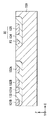
図1は、本技術の第1の実施の形態に係る表示装置(表示装置1)の断面構成を表したものである。この表示装置1は自発光型の表示装置であり、基板13の表面(面S1)に発光部20が設けられている。この発光部20は、基板13(面S1)と対向基板19との間に設けられている。対向基板19と基板13との間には、発光部20と共に、絶縁層14および素子分離層15が設けられている。これら発光部20、絶縁層14および素子分離層15は保護層16により覆われている。表示装置1は対向基板19側に光取り出し方向を有する、所謂トップエミッション型の表示装置であり、対向基板19の、基板13との対向面にはCF(カラーフィルタ)層17および反射部18が設けられている。基板13には、発光部20を駆動するためのトランジスタ(書込トランジスタTr1,駆動トランジスタTr2)が形成されている。基板13の裏面(面S2)側は支持部材11に固定されており、基板13と支持部材11との間には多層配線層12が設けられている。
<First Embodiment>
[Overall configuration of display device]
FIG. 1 illustrates a cross-sectional configuration of a display device (display device 1) according to a first embodiment of the present technology. The
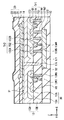
図2は、表示装置1の全体構成を表すものである。表示装置1は、基板13の中央部に表示領域110を有しており、例えば極薄型の有機発光カラーディスプレイ装置などとして用いられる。表示領域110の周辺には、例えば映像表示用のドライバである信号線駆動回路120、走査線駆動回路130および電源供給線駆動回路140が設けられている。
FIG. 2 shows the overall configuration of the
表示領域110には、マトリクス状に二次元配置された複数の画素10と、それらを駆動するための画素駆動回路150とが形成されている。一の画素10が例えば一の発光部20を有している。一の画素10が、例えば赤色、緑色、青色のうちいずれか一つを発光してもよく、あるいは一の画素10が赤色、緑色および青色を発光するようにしてもよい。画素駆動回路150において、列方向(Y方向)には複数の信号線120A(120A1,120A2,・・・,120Am,・・・)および複数の電源供給線140A(140A1,・・・,140An,・・・)が配置され、行方向(X方向)には複数の走査線130A(130A1,・・・,130An,・・・)が配置されている。信号線120Aと走査線130Aとの交差点に、一の画素10が設けられている。信号線120Aはその両端が信号線駆動回路120に接続され、走査線130Aはその両端が走査線駆動回路130に接続され、電源供給線140Aはその両端が電源供給線駆動回路140に接続されている。
In the
信号線駆動回路120は、信号供給源(図示せず)から供給される輝度情報に応じた映像信号の信号電圧を、信号線120Aを介して選択された画素10に供給するものである。走査線駆動回路130は、入力されるクロックパルスに同期してスタートパルスを順にシフト(転送)するシフトレジスタなどによって構成されている。走査線駆動回路130は、各画素10への映像信号の書き込みに際し行単位でそれらを走査し、各走査線130Aに走査信号を順次供給するものである。信号線120Aには信号線駆動回路120からの信号電圧が、走査線130Aには走査線駆動回路130からの走査信号がそれぞれ供給されるようになっている。
The signal
電源供給線駆動回路140は、入力されるクロックパルスに同期してスタートパルスを順にシフト(転送)するシフトレジスタなどによって構成されている。電源供給線駆動回路140は、信号線駆動回路120による列単位の走査と同期して、各電源供給線140Aに対し、各々の両端から、互いに異なる第1電位および第2電位のいずれかを適宜供給する。これにより、後述する駆動トランジスタTr2の導通状態または非導通状態の選択が行われる。
The power supply
画素駆動回路150は、基板13および多層配線層12に設けられている。図3に、画素駆動回路150の一構成例を表す。画素駆動回路150は、書込トランジスタTr1および駆動トランジスタTr2と、その間のキャパシタ(保持容量)Csと、発光部20とを有するアクティブ型の駆動回路である。発光部20は、電源供給線140Aおよび共通電源供給線(GND)の間において駆動トランジスタTr2と直列に接続されている。書込トランジスタTr1および駆動トランジスタTr2は、例えばシリコン薄膜トランジスタ(TFT(Thin Film Transistor))であり、その構成は例えば逆スタガ構造(いわゆるボトムゲート型)であってもスタガ構造(トップゲート型)であってもよい。
The
書込トランジスタTr1は、例えばドレイン電極が信号線120Aと接続されており、信号線駆動回路120からの映像信号が供給されるようになっている。また、書込トランジスタTr1のゲート電極は走査線130Aと接続されており、走査線駆動回路130からの走査信号が供給されるようになっている。さらに、書込トランジスタTr1のソース電極は、駆動トランジスタTr2のゲート電極と接続されている。
For example, the drain electrode of the writing transistor Tr1 is connected to the
駆動トランジスタTr2は、例えばドレイン電極が電源供給線140Aと接続されており、電源供給線駆動回路140による第1電位または第2電位のいずれかに設定される。駆動トランジスタTr2のソース電極は、発光部20と接続されている。
The drive transistor Tr2 has a drain electrode connected to the
保持容量Csは、駆動トランジスタTr2のゲート電極(書込トランジスタTr1のソース電極)と、駆動トランジスタTr2のドレイン電極との間に形成されるものである。 The storage capacitor Cs is formed between the gate electrode of the drive transistor Tr2 (source electrode of the write transistor Tr1) and the drain electrode of the drive transistor Tr2.
[表示装置の要部構成]
次に、再び図1を参照して、基板13、発光部20および対向基板19などの詳細な構成について説明する。
[Main components of the display device]
Next, with reference to FIG. 1 again, detailed configurations of the
基板13はシリコン層(Si層)13Aと絶縁層13Bとを含み、例えばSi層13Aが面S1、絶縁層13Bが面S2をそれぞれ構成している。基板13を保持する支持部材11は、例えばシリコンにより構成されている。基板13のSi層13Aには、書込トランジスタTr1のソース・ドレイン領域131A,131Bおよび駆動トランジスタTr2のソース・ドレイン領域132A,132Bが設けられている。ソース・ドレイン領域131A,131Bおよびソース・ドレイン領域132A,132Bは、例えばSi層13Aの裏面(基板13の面S2との対向面)近傍のN型半導体ウェル領域(以下、N型ウェル領域という。P型半導体領域についても同様。)133中に設けられた、P型領域である。Si層13Aの裏面には、ゲート絶縁膜(図示せず)を介して、書込トランジスタTr1のゲート電極TG1、駆動トランジスタTr2のゲート電極TG2が設けられている。ゲート電極TG1,TG2は、例えば例えば白金(Pt),チタン(Ti),ルテニウム(Ru),モリブデン(Mo),銅(Cu),タングステン(W),ニッケル(Ni),アルミニウム(Al)およびタンタル(Ta)等の金属単体または合金等により構成されており、このような金属の周囲には絶縁性のサイドウォール(SW)が設けられている。
The
絶縁層13Bは導電性プラグ(導電性プラグ13W1,13W2,13W3,13W4,13W5)を有しており、この導電性プラグを介して、書込トランジスタTr1、駆動トランジスタTr2と多層配線層12の配線(配線121,122)とが電気的に接続されている。導電性プラグ13W1,13W2,13W3,13W4,13W5は、絶縁層13Bの接続孔に設けられた導電体である。配線122は例えば導電性プラグ13W2,13W4に接続されており、これにより、書込トランジスタTr1のソース・ドレイン領域131Aと駆動トランジスタTr2のゲート電極TG2とを電気的に接続している。駆動トランジスタTr2のソース・ドレイン領域132Bには導電性プラグ13W3が接続され、この導電性プラグ13W3は例えば電源供給線140Aに電気的に接続されている。駆動トランジスタTr2のソース・ドレイン領域132Aは導電性プラグ13W5を介して配線121に電気的に接続されている。N型ウェル領域133の外側には、基板13および絶縁層14を貫通する電極(貫通電極13V)が設けられており、この貫通電極13Vが配線121と発光部20(後述の第1電極21)、即ち駆動トランジスタTr2のソース・ドレイン領域132Aと発光部20とを電気的に接続している。貫通電極13Vは、例えば絶縁層14および基板13を貫通する孔にポリシリコン(Poly Si)またはタングステン(W)等の導電材を設けたものである。
The insulating
本実施の形態では、発光部20で発生した光の一部を受光するための受光部30が表示領域110(図2)内に設けられ、この受光部30は書込トランジスタTr1、駆動トランジスタTr2と隣り合う位置に配置されている。詳細は後述するが、これにより発光部20と受光部30とを近付けることができる。従って、発光部20から受光部30までの間の光量の減少を抑えることが可能となり、受光部30の感度を高めることができる。
In the present embodiment, a
受光部30は、例えばフォトダイオードにより構成されており、Si層13Aの裏面近傍のP型ウェル領域134およびP型ウェル領域134中のN型領域135を含んでいる。換言すれば、受光部30は基板13の内部に形成されている。この受光部30は、例えば画素10毎に設けられている。Si層13Aの裏面には、ゲート絶縁膜(図示せず)を介して、トランジスタTr3のゲート電極TG3が設けられ、このトランジスタTr3により受光部30の信号電荷がフローティング領域FDに転送されるようになっている。フローティング領域FDは、例えばP型ウェル領域134中のN型領域である。絶縁層13Bの導電性プラグ13W6,13W7は、それぞれフローティング領域FD、トランジスタTr3のゲート電極TG3に、接続されている。
The
この受光部30は、図4に示したように、各発光部20(画素10)からの光量の情報(発光情報20D)を検知すると共に外光の光量情報(外光情報LD)を取得し、光電変換した受光信号30Aを補正回路50に送るようになっている。補正回路50では、この受光信号30Aから外光の影響を除き、発光部20の発光状態のみに起因する発光強度を算出すると共に各画素10の光量に応じて補正信号50Aを画素駆動回路150に出力する。画素駆動回路150は、外部から入力される映像信号40Aにこの補正信号50Aを追加して処理を行い、補正映像信号41Aとして発光部20(画素10)に出力する。これにより、発光部20に印加される電圧および電流が制御されて、発光部20間の輝度ムラが抑えられる。
As shown in FIG. 4, the
発光部20は、基板13の面S1全面に設けられた絶縁層14上の所定の領域に配置されており、基板13(絶縁層14)側から、第1電極21、発光層を含む有機層22および第2電極23をこの順に有している。
The
第1電極21は画素10(発光部20)毎に設けられており、複数の第1電極21が絶縁層14上に互いに離間して配置されている。この第1電極21は陽極としての機能および反射層としての機能を備えたものであり、反射率が高く、かつ、正孔注入性も高い材料により構成されていることが望ましい。このような第1電極21としては、例えば、積層方向の厚み(以下、単に厚みと言う)が30nm以上1000nm以下であり、クロム(Cr),金(Au),白金(Pt),ニッケル(Ni),銅(Cu),モリブデン(Mo),タングステン(W),チタン(Ti),タンタル(Ta),アルミニウム(Al)あるいは銀(Ag)などの金属元素の単体または合金が挙げられる。第1電極21は、このような金属膜を積層して構成するようにしてもよい。第1電極21(発光部20)は、書込トランジスタTr1,駆動トランジスタTr2(基板13のN型ウェル領域133)の直上に、これと平面視で重なるように配置することが好ましい。このように第1電極21を配置することにより、書込トランジスタTr1,駆動トランジスタTr2に入射する外光が第1電極21で遮られるので、書込トランジスタTr1,駆動トランジスタTr2の動作点が光により変化するのを防ぐことができる。
The
第1電極21の表面(第2電極23との対向面)から側面は、素子分離層15で覆われており、この素子分離層15には発光部20の発光領域を規定するための開口が設けられている。即ち、この素子分離層15の開口により第1電極21の表面が露出する。素子分離層15は、発光領域を正確に所望の形状に制御すると共に、第1電極21と第2電極23との間の絶縁性および隣接する発光部20間の絶縁性を確保する役割を担っている。絶縁層14および素子分離層15には例えば、ポリイミド等の有機材料または酸化シリコン(SiO2),窒化シリコン(SiNx)および酸窒化シリコン(SiON)等の無機材料を用いることができる。絶縁層14の厚みは例えば100nm〜1000nm、素子分離層15の厚みは例えば50nm〜2500nmである。
The side surface from the surface of the first electrode 21 (the surface facing the second electrode 23) is covered with the
有機層22は、例えば、第1電極21側から、正孔注入層,正孔輸送層,発光層,電子輸送層および電子注入層(いずれも図示せず)をこの順に有している。全ての発光部20に共通して有機層22を設けるようにしてもよく、あるいは、発光部20毎に有機層22を設けるようにしてもよい。
The
正孔注入層は、正孔注入効率を高めるためのものであると共に、リークを防止するためのバッファ層である。正孔注入層は、例えば、厚みが1nm以上300nm以下であり、化1または化2に示したヘキサアザトリフェニレン誘導体により構成されている。
The hole injection layer is a buffer layer for improving hole injection efficiency and preventing leakage. The hole injection layer has, for example, a thickness of 1 nm to 300 nm and is made of the hexaazatriphenylene derivative shown in

正孔輸送層は、発光層への正孔輸送効率を高めるためのものである。正孔輸送層は、例えば、厚みが40nm程度であり、4,4′,4″−トリス(3−メチルフェニルフェニルアミノ)トリフェニルアミン(m−MTDATA)またはα−ナフチルフェニルジアミン(αNPD)により構成されている。 The hole transport layer is for increasing the efficiency of transporting holes to the light emitting layer. The hole transport layer has a thickness of about 40 nm, for example, and is made of 4,4 ′, 4 ″ -tris (3-methylphenylphenylamino) triphenylamine (m-MTDATA) or α-naphthylphenyldiamine (αNPD). It is configured.
発光層は例えば白色発光用の発光層であり、第1電極21と第2電極23との間に例えば赤色発光層,緑色発光層および青色発光層(いずれも図示せず)の積層体を有している。発光部20毎に、赤色発光層,緑色発光層および青色発光層のいずれか一つを設けるようにしてもよい。赤色発光層,緑色発光層および青色発光層は、電界をかけることにより、第1電極21から正孔注入層および正孔輸送層を介して注入された正孔の一部と、第2電極23から電子注入層および電子輸送層を介して注入された電子の一部とが再結合して、それぞれ赤色,緑色および青色の光を発生させるものである。
The light emitting layer is, for example, a light emitting layer for white light emission, and includes, for example, a laminate of a red light emitting layer, a green light emitting layer, and a blue light emitting layer (all not shown) between the
赤色発光層は、例えば、赤色発光材料,正孔輸送性材料,電子輸送性材料および両電荷輸送性材料のうち少なくとも1種を含んでいる。赤色発光材料は、蛍光性のものでも燐光性のものでもよい。赤色発光層は、例えば、厚みが5nm程度であり、4,4−ビス(2,2−ジフェニルビニン)ビフェニル(DPVBi)に2,6−ビス[(4’−メトキシジフェニルアミノ)スチリル]−1,5−ジシアノナフタレン(BSN)を30重量%混合したものにより構成されている。 The red light emitting layer includes, for example, at least one of a red light emitting material, a hole transporting material, an electron transporting material, and a both charge transporting material. The red light emitting material may be fluorescent or phosphorescent. The red light-emitting layer has, for example, a thickness of about 5 nm, and 2,4-bis [(4′-methoxydiphenylamino) styryl]-is added to 4,4-bis (2,2-diphenylbinine) biphenyl (DPVBi). It is composed of 30% by weight of 1,5-dicyanonaphthalene (BSN).
緑色発光層は、例えば、緑色発光材料,正孔輸送性材料,電子輸送性材料および両電荷輸送性材料のうち少なくとも1種を含んでいる。緑色発光材料は、蛍光性のものでも燐光性のものでもよい。緑色発光層は、例えば、厚みが10nm程度であり、DPVBiにクマリン6を5重量%混合したものにより構成されている。 The green light emitting layer includes, for example, at least one of a green light emitting material, a hole transporting material, an electron transporting material, and a charge transporting material. The green light emitting material may be fluorescent or phosphorescent. The green light emitting layer has a thickness of about 10 nm, for example, and is composed of DPVBi mixed with 5% by weight of coumarin 6.
青色発光層は、例えば、青色発光材料,正孔輸送性材料,電子輸送性材料および両電荷輸送性材料のうち少なくとも1種を含んでいる。青色発光材料は、蛍光性のものでも燐光性のものでもよい。青色発光層は、例えば、厚みが30nm程度であり、DPVBiに4,4’−ビス[2−{4−(N,N−ジフェニルアミノ)フェニル}ビニル]ビフェニル(DPAVBi)を2.5重量%混合したものにより構成されている。 The blue light emitting layer includes, for example, at least one of a blue light emitting material, a hole transporting material, an electron transporting material, and a charge transporting material. The blue light emitting material may be fluorescent or phosphorescent. For example, the blue light-emitting layer has a thickness of about 30 nm, and 2.5% by weight of 4,4′-bis [2- {4- (N, N-diphenylamino) phenyl} vinyl] biphenyl (DPAVBi) is added to DPVBi. It is composed of a mixture.
電子輸送層は、発光層への電子輸送効率を高めるためのものであり、例えば厚みが20nm程度の8−ヒドロキシキノリンアルミニウム(Alq3)により構成されている。電子注入層は、発光層への電子注入効率を高めるためのものであり、例えば厚みが0.3nm程度のLiFあるいはLi2O等により構成されている。 The electron transport layer is for increasing the efficiency of electron transport to the light emitting layer, and is made of, for example, 8-hydroxyquinoline aluminum (Alq3) having a thickness of about 20 nm. The electron injection layer is for increasing the efficiency of electron injection into the light emitting layer, and is made of, for example, LiF or Li 2 O having a thickness of about 0.3 nm.
第2電極23は、有機層22を間にして第1電極21と対をなし、第1電極21と絶縁された状態で例えば電子注入層の上に発光部20(画素10)に共通して設けられている。第2電極23は、光透過性の透明材料からなり、例えば、アルミニウム(Al),マグネシウム(Mg),銀(Ag),カルシウム(Ca)またはナトリウム(Na)の合金により構成されている。中でも、マグネシウムと銀との合金(Mg−Ag合金)は、薄膜での導電性と吸収の小ささとを兼ね備えているので好ましい。Mg−Ag合金におけるマグネシウムと銀との比率は特に限定されないが、膜厚比でMg:Ag=20:1〜1:1の範囲であることが望ましい。また、第2電極23の材料には、アルミニウム(Al)とリチウム(Li)との合金(Al−Li合金)を用いるようにしてもよく、インジウム錫酸化物(ITO),酸化亜鉛(ZnO),アルミナドープ酸化亜鉛(AZO),ガリウムドープ酸化亜鉛(GZO),インジウム亜鉛酸化物(IZO),インジウムチタン酸化物(ITiO)またはインジウムタングステン酸化物(IWO)等を用いてもよい。
The
保護層16は、第2電極23を覆うように基板13の全面に設けられ、例えば、ポリイミドなどの絶縁性樹脂材料により構成されている。対向基板19の一方の面(基板13との対向面)に設けられたCF層17は、赤色カラーフィルタ17R,緑色カラーフィルタ(図示せず)および青色カラーフィルタ17Bを有しており、これらがそれぞれの発光部20(画素10)に対応して順に配置されている。CF層17は、対向基板19のどちら側の面に設けられてもよいが、発光部20の側に設けられることが好ましい。カラーフィルタが表面に露出せず、保護層16(または接着層)により保護することができるからである。また、有機層22とカラーフィルタとの間の距離が狭くなることにより、有機層22から出射した光が隣接する他の色のカラーフィルタに入射して混色を生じることを避けることができるからである。
The
反射部18は、発光部20で発生した光のうち、対向基板19に向かう光を反射して基板13内の受光部30へ集めるためのものであり、例えば受光部30と対向する領域に画素10毎に設けられている。この反射部18には例えばアルミニウム,タングステン,銀またはチタン等の反射率の高い金属膜を用いることができる。このような金属に、窒化チタン(TiN)などの窒化物または酸化物を積層して反射部18を構成するようにしてもよい。例えば、対向基板19側から、窒化チタンおよびアルミニウムを積層させた反射部18は、表示面側での反射を抑えると共に、発光部20からの光を効率よく反射させて受光部30に入射させることができる。反射部18と共に、隣り合う画素10間での光漏れを防止するための遮光部(図示せず)を設けるようにしてもよく、例えばアルミニウムからなる反射部18と窒化チタンからなる遮光部とを積層するようにしてもよい。対向基板19は、熱硬化型樹脂などの接着層(図示せず)などと共に発光部20を封止するものであり、有機層22において発生した光を透過する透明なガラスまたはプラスチック材料により構成されている。
The
[表示装置の製造方法]
このような表示装置1は、例えば次のようにして製造することができる(図5A〜図6B)。
[Display device manufacturing method]
Such a
まず、基板13を形成する。具体的には、最初に、Si層13Aの一方の面の近傍に例えばイオン注入によりN型ウェル領域133、書込トランジスタTr1のソース・ドレイン領域131A,131B、駆動トランジスタTr2のソース・ドレイン領域132A,132B、P型ウェル領域134、N型領域135、フローティング領域FDを形成する(図5A)。Si層13Aには、例えば、SOI(Silicon On Insulator)基板を用いることができる。次いで、上記不純物拡散領域を設けたSi層13Aの面上にゲート絶縁膜(図示せず)を介して書込トランジスタTr1,駆動トランジスタTr2,トランジスタTr3のゲート電極TG1,TG2,TG3を形成する。このゲート電極TG1,TG2,TG3は、導電膜を例えばCVD(Chemical Vapor Deposition)法により成膜した後、これをドライエッチングすることにより形成することができる。この後、ゲート電極TG1,TG2,TG3を覆うように絶縁層13Bを成膜する。これにより基板13が形成される。このとき、絶縁層13Bには導電性プラグ13W1,13W2,13W3,13W4,13W5,13W6,13W7を設けておく。基板13を形成した後、基板13の絶縁層13B上(基板13の面S2上)に多層配線層12(配線121,配線122)を形成する(図5B)。
First, the
続いて、この多層配線層12に支持部材11(図1)を接合した後、支持部材11、多層配線層12および基板13を反転し、Si層13Aの他方の面(N型ウェル領域133およびP型ウェル領域134等の形成面とは反対側の面)側からSi層13Aが所望の厚さになるよう、例えばCMP(Chemical Mechanical Polishing)により研磨する(図5C)。この研磨された面が基板13の面S1となる。例えばCMP工程の前にグラインダーによる荒研磨、CMP工程後にホットリン酸等の薬液を用いたSi層13Aの平坦化を行う。Si層13Aの研磨は、次いで、この基板13の面S1上に絶縁層14を成膜した後、貫通電極13Vを形成する。貫通電極13Vは、例えば絶縁層14および基板13を貫通する孔を設けた後、この孔に導電材料を埋め込み、CMPを行って形成する。
Subsequently, after the support member 11 (FIG. 1) is joined to the
次いで、絶縁層14上に例えばアルミニウムをスパッタ法により成膜した後、これをフォトリソグラフィ工程を用いてパターニングし、第1電極21を形成する。続いて、第1電極21および絶縁層14上に例えばプラズマCVD法により例えば窒化シリコン膜を成膜した後、この窒化シリコン膜に開口を設けて素子分離層15を形成する。素子分離層15の形成にSTI(Shallow trench isolation)を用いるようにしてもよい。
Next, for example, aluminum is deposited on the insulating
素子分離層15を設けた後、例えば蒸着法により発光層を含む有機層22および第2電極13を形成する(図5D)。このようにして発光部20を設けた後、例えばCVD法またはスパッタ法により、発光部20の上に保護層16を形成する。
After providing the
一方、対向基板19の表面には反射部18およびCF層17を例えばこの順に形成する(図6A,図6B)。この後、CF層17を設けた対向基板19の周縁にシール剤を塗布し、これを保護層16を設けた基板13と貼り合わせる。最後に、基板13と対向基板19との間の間隙に充填剤を注入した後、これを封止して表示装置1を完成させる。
On the other hand, the
[表示装置の動作]
この表示装置1では、各画素10に対して走査線駆動回路130から書込トランジスタTr1のゲート電極TG1を介して走査信号が供給されると共に、信号線駆動回路120から画像信号が書込トランジスタTr1を介して保持容量Csに保持される。すなわち、この保持容量Csに保持された信号に応じて駆動トランジスタTr2がオンオフ制御され、これにより、各発光部20に駆動電流Idが注入されることにより、正孔と電子とが再結合して発光が起こる。図7に示したように、この光(光L1)は、第2電極23,CF層17および対向基板19を透過して取り出される。
[Operation of display device]
In the
一方、発光部20で発生した光の一部(光L2)は、反射部18で反射されて、基板13の受光部30に入射する。この受光部30からの受光信号30A(図4)を受け、補正回路50は例えば以下のようにして補正信号50Aを画素駆動回路150に送る(図8)。まず、発光部20の消光時、点灯時にそれぞれ受光部30を駆動して、外光情報LDおよび発光情報20Dを取得する。受光部30の駆動前には、受光部30を初期化しておく。この受光部30で検知された外光情報LDおよび発光情報20DはADC(Analog to Digital Converter)にてデジタル変換された後、保存される。このデジタル変換および保存の際には、例えば発光部20は消灯している。補正回路50では、発光情報20Dのデジタルデータから外光情報LDのデジタルデータを減算することにより、発光部20のみに起因した各画素10の発光強度を算出した後、各画素10の発光状態と対象画素の発光状態とを比較して各画素10の輝度に応じた補正信号50Aを生成する。例えばこのタイミングで補正回路50は新たな補正情報に更新される。画素駆動回路150は、DAC(Digital to Analog Converter)にて変換した映像信号40Aに補正信号50Aを追加し、補正映像信号41Aを発光部20に送る。このような補正信号50Aの取得と映像出力とは連続していなくてもよい。例えば映像出力60フレームに一度、補正信号50Aを取得するようにしてもよく、あるいは電源のオン、オフ時に補正信号50Aを取得するようにしてもよい。発光部20および補正回路50の動作は、補正情報の更新のタイミングによって適宜変更することが可能である。外光情報LDおよび発光情報20Dの光量が受光部30の受光量を超える場合にエラーとなるように設定してもよいし、あるいは、再度受光するように設定しておいてもよい。なお、ADCおよびDACは補正回路50に含まれていてもよく、補正回路50の外部に設けるようにしてもよい。
On the other hand, part of the light (light L <b> 2) generated by the
[表示装置の作用・効果]
ここでは、表示領域110内に受光部30が設けられているので、発光部20と受光部30との距離を短くして、発光部20からの光を感度よく、精確に検知することができる。よって、より効果的に輝度ムラを抑えることができる。以下、これについて説明する。
[Operation and effect of display device]
Here, since the
図9は比較例に係る表示装置(表示装置100)の平面構成を模式的に表したものである。この表示装置100の受光部300は表示領域110の外側の領域に配置されている。このため、それぞれの画素10(発光部)と受光部300との間の距離が長くなってしまう。また、各画素により受光部300との間の距離が異なるため、補正回路では発光部の劣化に加えて、各画素と受光部300との間の距離による光の減衰を考慮しなければならない。
FIG. 9 schematically shows a planar configuration of a display device (display device 100) according to a comparative example. The
輝度ムラを抑える方法として、表示装置の映像を外部の撮像装置に取り込む方法も提案されている(例えば、特開2011−77825号公報参照)。しかし、この方法では、映像の取り込みの精度が操作者によって左右されるため、発光部からの光を精確に検知することができない。この他、複数のトランジスタと容量素子とを組み合わせることにより、画素を駆動するためのトランジスタの性能のバラツキを調整することも可能である(例えば、特開2010−145579号公報参照)。しかしこの方法では、発光部の劣化に伴う各画素間の輝度ムラを補正することができない。また、画素のピッチが微細化すると、容量素子の面積が小さくなるため、十分な容量を得ることが困難となる。 As a method for suppressing luminance unevenness, a method of capturing an image of a display device into an external imaging device has also been proposed (see, for example, JP 2011-77825 A). However, this method cannot accurately detect light from the light emitting unit because the accuracy of capturing the image depends on the operator. In addition, by combining a plurality of transistors and a capacitor, variation in the performance of the transistors for driving the pixels can be adjusted (see, for example, Japanese Patent Application Laid-Open No. 2010-145579). However, this method cannot correct luminance unevenness between pixels due to deterioration of the light emitting section. Further, when the pixel pitch is miniaturized, it is difficult to obtain a sufficient capacitance because the area of the capacitive element is reduced.
これに対し表示装置1では、表示領域110(図2)内に受光部30が設けられているので、各発光部20(画素10)毎に基板13の内部に受光部30を配置して、発光部20と受光部30との間の距離を近付けることが可能となる。発光部20は、発光部20を駆動するためのトランジスタ(書込トランジスタTr1,駆動トランジスタTr2)の直上に設けられ、受光部30は、例えばこのトランジスタと隣り合う位置に画素10毎に配置される。よって、基板13の面内方向(XY平面)における発光部20と受光部30との距離が短くなり、例えばマイクロOLED(Organc Light Emitting Diode)等の画素ピッチの小さいディスプレイにも適用することが可能となる。
On the other hand, in the
図10に示したように、基板13の面S1上に多層配線層(多層配線層212)を設けることも可能であるが、このような構成では、基板13の面(面S1,S2)に対して垂直方向(Z方向の距離)における発光部20と受光部30との距離が遠くなってしまう。また、多層配線層212中に発光部20からの光を受光部30に導くための導波路構造が必要となる。このため、基板13の表面(面S1)に発光部20、裏面(面S2)に多層配線層12をそれぞれ設けて、基板13の面に対して垂直方向における発光部20と受光部30との距離も狭めることが好ましい。
As shown in FIG. 10, it is possible to provide a multilayer wiring layer (multilayer wiring layer 212) on the surface S1 of the
以上のように本実施の形態の表示装置1では、表示領域110内に受光部30を設けるようにしたので、発光部20と受光部30との間の距離を小さくすることができる。即ち、発光部20と受光部30との間での光量の減少を抑えることが可能となり、受光部30はより精確に受光信号30Aを補正回路50に送ることができる。よって、表示領域110内での各画素10間の輝度ムラを抑えることができる。
As described above, in the
以下、上記実施の形態の変形例および他の実施の形態について説明するが、以降の説明において上記実施の形態と同一構成部分については同一符号を付してその説明は適宜省略する。 Hereinafter, modifications of the above-described embodiment and other embodiments will be described. In the following description, the same components as those of the above-described embodiment will be denoted by the same reference numerals, and the description thereof will be omitted as appropriate.
<変形例1>
図11は、変形例1に係る表示装置(表示装置1A)の断面構成を表したものである。この表示装置1Aの反射部(反射部18A)は所謂パラボラ形状であり、基板13に対向して放物曲面を有している。この点を除き、表示装置1Aは表示装置1と同様の構成を有し、その作用および効果も同様である。
<
FIG. 11 illustrates a cross-sectional configuration of a display device (
反射部18Aの放物曲面は受光部30に焦点を有するものであり、図12に示したように、発光部20から反射部18Aに向かう光(光L2)は、反射部18Aから受光部30に効率よく集光される。従って、発光部20から反射部18Aにより受光部30に入射する光の光量を増やし、より高い精度で各画素10の輝度を補正することが可能となる。
The parabolic curved surface of the reflecting
反射部18Aは、例えば以下のようにして形成することができる。まず、対向基板19のうち、反射部18Aの形成予定領域に放物曲面を有する凹部19Cを形成する(図13)。具体的には、対向基板19の表面にレジストを設けた後、例えばフォトリソグラフィ工程により露光量を調整してレジストに放物曲面を形成する。即ち、レジストを中心部が薄く、かつ、周囲を厚くした形状に成形する。このレジストの放物曲面はハーフトーンマスクを用いて形成してもよく、あるはリフロー工程により形成することも可能である。この放物曲面を有するレジストを用いて例えばプラズマエッチングを行うことにより、対向基板19に凹部19Cが形成される。凹部19Cを設けた後、対向基板19の全面に例えば反射率の高い金属膜を成膜した後、反射部18Aの形成予定領域にレジストでマスクを形成してプラズマエッチングまたはウェットエッチングを行う。最後にレジストを除去して反射部18Aを形成する。図14に示したように、対向基板19の矩形状の凹部19Cに金属膜を成膜した後、例えばCMP等によりこの金属膜を削って反射部18Aを形成することも可能である。反射部18Aを形成する際には、対向基板19に、反射部18Aが設けられる凹部19C1と共に反射部18Aのアラインメント用の凹部19C2を設けておくことが好ましい(図15)。
The
<第2の実施の形態>
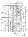
図16は、第2の実施の形態に係る表示装置(表示装置2)の断面構成を表したものである。この表示装置2は、書込トランジスタTr1,駆動トランジスタTr2と受光部30との間に遮蔽部(遮蔽部31)を有するものである。この点を除き、表示装置2は表示装置1と同様の構成を有し、その作用および効果も同様である。
<Second Embodiment>
FIG. 16 illustrates a cross-sectional configuration of a display device (display device 2) according to the second embodiment. This
遮蔽部31は、例えばSi層13Aの溝に設けたシリコン酸化膜およびシリコン窒化膜等の絶縁膜またはタングステン,チタンおよび窒化チタン等の金属膜である。絶縁膜および金属膜を重ねて遮蔽部31を構成するようにしてもよく、例えばSi層13Aの溝にシリコン酸化膜、シリコン窒化膜、チタンまたは窒化チタンおよびタングステンをこの順に積層するようにしてもよい。Si層13Aの溝は、書込トランジスタTr1,駆動トランジスタTr2および受光部30の形成領域の深さまで設けられていればよいが(図16)、Si層13Aを貫通していてもよい(図17A)。遮蔽部31の形状は、テーパ状(図16)であってもよく、柱状(図17B)であってもよい。遮蔽部31は、書込トランジスタTr1,駆動トランジスタTr2の設けられたN型ウェル領域133と受光部30の設けられたP型ウェル領域134との間に配置されており、受光部30(P型ウェル領域134)を囲んでいる(図18A,図18B)。遮蔽部31はN型ウェル領域133を囲むようにしてもよく(図18C)、あるいはP型ウェル領域134およびN型ウェル領域133を囲んでいてもよい(図18D)。
The shielding
このような遮蔽部31を設けることにより、より精確に発光部20からの光を受光部30で検知することができる。以下、これについて詳細に説明する。図19に示したように、発光部20で光が発生することにより、基板13(Si層13A)の温度が上昇し、余剰キャリア(キャリアC)が発生する。反射部18で反射されて基板13に入射した光のうち、受光部30以外の部分に入射した光もこのようなキャリアCの発生原因となる。遮蔽部31は、このような受光部30の外側で発生したキャリアCが受光部30内に浸入するのを防ぐためのものである。即ち、遮蔽部31を設けることにより、キャリアCの受光部30への浸入が遮断され、より精確に各発光部20からの光を受光部30が検知する。
By providing such a
遮蔽部31は、例えば、図20に示したように、Si層13Aに受光部30(Pウェル領域134およびN型領域135)およびフローティング領域FDを設けた後、例えば受光部30の周囲に溝を形成し、この溝に絶縁膜を埋め込んで形成する。絶縁膜を埋め込んだ後、例えばCMP等により研磨するようにしてもよい。遮蔽部31は、例えば基板13と対向基板19との位置合わせをおこなうためのマーク(例えばBSA(Back Side Alignment))と共に形成することも可能である。あるいは、Si層13Aを研磨した後(図5C)、貫通電極13Vと共に上記絶縁膜または金属膜からなる遮蔽部31を形成するようにしてもよい。貫通電極13Vと共に遮蔽部31を形成することで、エッチング加工工程を単純化することができる。
For example, as illustrated in FIG. 20, the shielding
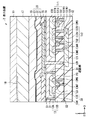
<変形例2>
図21に示したように、受光部30の周囲に例えば、銅,タングステンおよびアルミニウム等の遮光性の高い金属膜を含む遮蔽部(遮蔽部32)を設けるようにしてもよい(変形例2)。この遮蔽部32を有する表示装置2Aでは、受光部30から隣り合う画素10および書込トランジスタTr1,駆動トランジスタTr2の形成領域への光の漏れだしが抑えられ、受光部30に発光部20からの光をより効率よく集めることができる。遮蔽部32は、上記第2の実施の形態の遮蔽部31と同様に、Si層13Aの溝に設けられており、この溝に例えば絶縁膜および金属膜をこの順に埋め込んで形成する。この絶縁膜には、例えばシリコン酸化膜またはシリコン窒化膜等を用いることが可能である。
<
As shown in FIG. 21, for example, a shielding part (shielding part 32) including a highly light-shielding metal film such as copper, tungsten, and aluminum may be provided around the light receiving part 30 (Modification 2). . In the display device 2A having the shielding
<第3の実施の形態>
図22は、第3の実施の形態に係る表示装置(表示装置3)の要部の断面構成を表したものである。この表示装置3では、基板(基板43)の表面に発光部20と共に受光部(受光部50)が設けられている。この点を除き、表示装置2は表示装置1と同様の構成を有し、その作用および効果も同様である。図22では、保護層16、CF層17および対向基板19(図1等)を省略した。
<Third Embodiment>
FIG. 22 illustrates a cross-sectional configuration of a main part of a display device (display device 3) according to the third embodiment. In the
基板43は、例えば板状部材43AにTFT層43Bを積層したものにより構成されており、TFT層43B上に発光部20および受光部50が設けられている。板状部材43Aは、例えば、石英、ガラス、シリコン(Si)、金属箔、もしくは樹脂製のフィルムやシートなどにより構成されている。TFT層43Bには、発光部20を駆動するためのトランジスタ、例えば書込トランジスタTr1および駆動トランジスタTr2(図3)が設けられている。TFT層43Bには、発光部20および受光部50に接続された配線も設けられている。
The
受光部50は、平面視で発光部20と隣り合う位置に、例えば、画素10(図2)毎に配置されている。この受光部50は基板43側から、下部電極51、光電変換膜52および上部電極53を有するものであり、発光部20からの光を受けて信号電荷(例えば電子)を生成する。この信号電荷は、下部電極51から取り出され、受光信号30Aとして補正回路50に送られるようになっている(図4)。下部電極51、光電変換膜52および上部電極53は、受光部50毎にパターニングされている。
The
下部電極51は、例えば発光部20の第1電極21と同層に設けられており、例えばTFT層43Bの配線を介して補正回路50(図4)に電気的に接続されている。この下部電極51には、第1電極21と同様の材料、例えばアルミニウムを用いることができる。光電変換膜52は、発光部20で発生した波長の光(可視光)を吸収して、電子・ホール対を発生させるものであり、例えば、CIGS(Copper Indium Gallium Selenide)または有機光電変換材料などにより構成されている。上部電極53は、この光電変換膜52で発生した電子・ホール対の一方(例えばホール)を排出するためのものであり、例えば、TFT層43Bの配線を介してGNDに電気的に接続されている。上部電極53には、例えば発光部20の第2電極23と同様の光透過性導電材料を用いることができる。この上部電極53は素子分離層15に覆われており、更にこの素子分離層15は発光部20から延在する有機層22および第2電極23により覆われている。表示装置1と同様に、受光部50と対向する位置に反射部18を設けるようにしてもよい(図1)。
The
このような表示装置3は、例えば以下のようにして製造することができる(図23A〜図25C)。
Such a
まず、基板43の表面全面に例えばスパッタ法により導電膜51Mを成膜した後(図23A)、これをドライエッチングまたはウェットエッチングによりパターニングして、下部電極51を形成する(図23B)。導電膜51Mから、下部電極51と同時に第1電極21を形成するようにしてもよい。
First, a conductive film 51M is formed on the entire surface of the
次いで、基板43の全面に光電変換膜52Mを例えばスパッタリング法により成膜した後(図23C)、これをパターニングして下部電極51の上面および側面を覆う光電変換膜52を形成する(図24A)。続いて、例えば基板43の全面に光透過性の導電膜53Mを成膜した後(図24B)、この導電膜53Mをパターニングして光電変換膜52上に上部電極53を形成する(図24C)。上部電極53は、例えば光電変換膜52の上面および側面を覆っている。これにより、受光部50が形成される。受光部50を設けた後、基板43の全面に絶縁膜15Mを成膜する(図25A)。この絶縁膜15Mの一部に開口を設けて第1電極21の表面を露出させ、素子分離層15を形成する(図25B)。素子分離層15を設けた後、基板43の全面に有機層22および第2電極23をこの順に成膜して、発光部20を形成する(図25C)。以降の工程は表示装置1と同様に行い、表示装置3を完成させる。
Next, a
この表示装置3の受光部50は、表示装置1の受光部30(図1、図7)と同様にして発光部20で発生した光の一部を受光する。基板43の表面の受光部50は、基板13の内部の受光部30よりも発光部20により近い位置に設けられているので、反射部18を介さずに、発光部20で発生した光を直接受けることが可能となる。よって、発光部20から受光部50までの間の光量の減少を抑えて、より精確な受光信号30Aを補正回路50に送ることが可能となる。
The
(モジュール)
上記実施の形態および変形例の表示装置1,1A,2,2A,3(以下、単に表示装置と表す)は、例えば、図26に示したようなモジュールとして、後述する適用例1〜5などの種々の電子機器に組み込まれる。このモジュールは、例えば、基板13,43の一辺に、対向基板19から露出した領域210を設け、この露出した領域210に、信号線駆動回路120および走査線駆動回路130の配線を延長して外部接続端子(図示せず)を形成したものである。外部接続端子には、信号の入出力のためのフレキシブルプリント配線基板(FPC;Flexible Printed Circuit)220が設けられていてもよい。
(module)
The
(適用例1)
図27は、上記実施の形態の表示装置1が適用されるテレビジョン装置の外観を表したものである。このテレビジョン装置は、例えば、フロントパネル310およびフィルターガラス320を含む映像表示画面部300を有しており、この映像表示画面部300は、上記各実施の形態に係る表示装置により構成されている。
(Application example 1)
FIG. 27 illustrates an appearance of a television device to which the
(適用例2)
図28A,28Bは、上記実施の形態の表示装置が適用されるデジタルカメラの外観を表したものである。このデジタルカメラは、例えば、フラッシュ用の発光部410、表示部420、メニュースイッチ430およびシャッターボタン440を有しており、その表示部420は、上記各実施の形態に係る表示装置により構成されている。
(Application example 2)
28A and 28B show the appearance of a digital camera to which the display device of the above embodiment is applied. The digital camera includes, for example, a flash light emitting unit 410, a display unit 420, a menu switch 430, and a
(適用例3)
図29は、上記実施の形態の表示装置1が適用されるノート型パーソナルコンピュータの外観を表したものである。このノート型パーソナルコンピュータは、例えば、本体510,文字等の入力操作のためのキーボード520および画像を表示する表示部530を有しており、その表示部530は、上記各実施の形態に係る表示装置により構成されている。
(Application example 3)
FIG. 29 shows an appearance of a notebook personal computer to which the
(適用例4)
図30は、上記実施の形態の表示装置が適用されるビデオカメラの外観を表したものである。このビデオカメラは、例えば、本体部610,この本体部610の前方側面に設けられた被写体撮影用のレンズ620,撮影時のスタート/ストップスイッチ630および表示部640を有しており、その表示部640は、上記各実施の形態に係る表示装置により構成されている。
(Application example 4)
FIG. 30 shows the appearance of a video camera to which the display device of the above embodiment is applied. This video camera has, for example, a main body 610, a
(適用例5)
図31A,31Bは、上記実施の形態の表示装置が適用される携帯電話機の外観を表したものである。この携帯電話機は、例えば、上側筐体710と下側筐体720とを連結部(ヒンジ部)730で連結したものであり、ディスプレイ740,サブディスプレイ750,ピクチャーライト760およびカメラ770を有している。そのディスプレイ740またはサブディスプレイ750は、上記各実施の形態に係る表示装置により構成されている。
(Application example 5)
31A and 31B show the appearance of a mobile phone to which the display device of the above embodiment is applied. For example, the mobile phone is obtained by connecting an
以上、実施の形態および変形例を挙げて本技術を説明したが、本技術は上記実施の形態等に限定されるものではなく、種々変形が可能である。例えば、上記実施の形態等において説明した各層の材料および厚み、または成膜方法および成膜条件等は限定されるものではなく、他の材料および厚みとしてもよく、または他の成膜方法および成膜条件としてもよい。 Although the present technology has been described with the embodiment and the modification, the present technology is not limited to the above-described embodiment and the like, and various modifications can be made. For example, the material and thickness of each layer described in the above embodiment and the like, or the film formation method and film formation conditions are not limited, and other materials and thicknesses may be used. It is good also as film | membrane conditions.
また、上記実施の形態等では、第1電極21を陽極、第2電極23を陰極とする場合について説明したが、陽極および陰極を逆にして、第1電極21を陰極、第2電極23を陽極としてもよい。更に、本技術をボトムエミッション型の表示装置に適用してもよい。
In the above-described embodiment and the like, the case where the
加えて、本技術を例えば発光部20に無機層を有する無機EL表示装置等、有機EL表示装置以外の自発光型の表示装置に適用することも可能である。
In addition, the present technology can be applied to a self-luminous display device other than the organic EL display device, such as an inorganic EL display device having an inorganic layer in the
更にまた、上記実施の形態等では、書込トランジスタTr1,駆動トランジスタTr2の構成を具体的に説明したが、これらの配置は逆であってもよく、あるいは発光部20の直下に他のトランジスタを配置するようにしてもよい。加えて、上記実施の形態等では、書込トランジスタTr1,駆動トランジスタTr2のソース・ドレイン領域をN型ウェル領域内に、受光部30をP型ウェル領域内にそれぞれ設けるようにしたが、書込トランジスタTr1,駆動トランジスタTr2のソース・ドレイン領域P型ウェル領域内に、受光部30をN型ウェル領域内に設けることも可能である。
Furthermore, in the above-described embodiment and the like, the configuration of the write transistor Tr1 and the drive transistor Tr2 has been specifically described. However, these arrangements may be reversed, or another transistor may be provided directly under the
なお、本技術は以下のような構成も取ることができる。
(1)表示領域内に、発光部と、前記発光部からの光を受光する受光部とを有する表示装置。
(2)更に、前記発光部を駆動する画素駆動回路と、前記受光部の受光量に応じて前記画素駆動回路に補正信号を送る補正回路とを有する前記(1)に記載の表示装置。
(3)前記発光部および前記受光部は、基板の表面に設けられている前記(1)または(2)に記載の表示装置。
(4)前記受光部は、一対の電極の間に光電変換膜を有している前記(1)乃至(3)のうちいずれか1つに記載の表示装置。
(5)前記発光部は基板の表面に設けられ、前記受光部は前記基板の内部に設けられている前記(2)に記載の表示装置。
(6)前記受光部はフォトダイオードにより構成されている前記(5)に記載の表示装置。
(7)前記基板はシリコン層を有する前記(5)または(6)に記載の表示装置。
(8)前記シリコン層の裏面近傍に前記受光部が設けられている前記(7)に記載の表示装置。
(9)前記画素駆動回路はトランジスタを含み、前記トランジスタが前記発光部と平面視で重なる位置に設けられている前記(5)乃至(8)のうちいずれか1つに記載の表示装置。
(10)前記トランジスタおよび前記受光部を画素毎に有し、前記トランジスタと前記受光部とは互いに隣り合う位置に設けられている前記(9)に記載の表示装置。
(11)前記トランジスタと前記受光部との間に遮蔽部を有する前記(10)に記載の表示装置。
(12)前記遮蔽部は、前記基板の溝に埋設された絶縁膜である前記(11)に記載の表示装置。
(13)前記遮蔽部は、前記基板の溝に埋設された金属膜である前記(11)に記載の表示装置。
(14)前記遮蔽部は、前記基板の溝に埋設された銅である前記(11)に記載の表示装置。
(15)前記受光部を囲むように前記遮蔽部が設けられている前記(11)乃至(14)のうちいずれか1つに記載の表示装置。
(16)前記基板と対向する反射部を有し、前記反射部で反射された前記発光部からの光が前記受光部に入射する前記(5)乃至(15)のうちいずれか1つに記載の表示装置。
(17)前記反射部の前記基板との対向面は放物曲面である前記(16)に記載の表示装置。
(18)表示装置を備え、前記表示装置は、表示領域内に、発光部と、前記発光部からの光を受光する受光部とを有する電子機器。
(19)画素駆動回路により表示領域内の発光部を駆動し、前記発光部からの光を前記表示領域内の受光部で受光し、前記受光部の受光量に応じて補正回路から前記画素駆動回路に補正信号を送る表示装置の駆動方法。
(20)表示領域内に、発光部と前記発光部からの光を受光する受光部とを形成する表示装置の製造方法。
In addition, this technique can also take the following structures.
(1) A display device having a light emitting unit and a light receiving unit that receives light from the light emitting unit in a display area.
(2) The display device according to (1), further including: a pixel driving circuit that drives the light emitting unit; and a correction circuit that sends a correction signal to the pixel driving circuit in accordance with the amount of light received by the light receiving unit.
(3) The display device according to (1) or (2), wherein the light emitting unit and the light receiving unit are provided on a surface of a substrate.
(4) The display device according to any one of (1) to (3), wherein the light receiving unit includes a photoelectric conversion film between a pair of electrodes.
(5) The display device according to (2), wherein the light emitting unit is provided on a surface of the substrate, and the light receiving unit is provided inside the substrate.
(6) The display device according to (5), wherein the light receiving unit includes a photodiode.
(7) The display device according to (5) or (6), wherein the substrate has a silicon layer.
(8) The display device according to (7), wherein the light receiving unit is provided in the vicinity of the back surface of the silicon layer.
(9) The display device according to any one of (5) to (8), wherein the pixel driving circuit includes a transistor, and the transistor is provided at a position overlapping the light emitting unit in plan view.
(10) The display device according to (9), wherein the transistor and the light receiving unit are provided for each pixel, and the transistor and the light receiving unit are provided at positions adjacent to each other.
(11) The display device according to (10), further including a shielding portion between the transistor and the light receiving portion.
(12) The display device according to (11), wherein the shielding portion is an insulating film embedded in a groove of the substrate.
(13) The display device according to (11), wherein the shielding portion is a metal film embedded in a groove of the substrate.
(14) The display device according to (11), wherein the shielding portion is copper embedded in a groove of the substrate.
(15) The display device according to any one of (11) to (14), wherein the shielding portion is provided so as to surround the light receiving portion.
(16) The optical system according to any one of (5) to (15), further including a reflecting unit facing the substrate, wherein light from the light emitting unit reflected by the reflecting unit is incident on the light receiving unit. Display device.
(17) The display device according to (16), wherein a surface of the reflecting portion facing the substrate is a parabolic surface.
(18) An electronic apparatus including a display device, wherein the display device includes a light emitting unit and a light receiving unit that receives light from the light emitting unit in a display area.
(19) The pixel driving circuit drives the light emitting section in the display area, the light from the light emitting section is received by the light receiving section in the display area, and the pixel driving from the correction circuit according to the amount of light received by the light receiving section. A display device driving method for sending a correction signal to a circuit.
(20) A method for manufacturing a display device, wherein a light emitting portion and a light receiving portion that receives light from the light emitting portion are formed in a display area.
1,1A,2,2A,3・・・表示装置、10・・・画素、11・・・支持部材、12・・・多層配線層、13,43・・・基板、13A・・・Si層、13B・・・絶縁層、43A・・・板状部材、43B・・・TFT層、13V・・・貫通電極、13W1,13W2,13W3,13W4,13W5,13W6,13W7・・・導電性プラグ、Tr1,Tr2,Tr3・・・トランジスタ、TG1,TG2,TG3・・・ゲート電極、14・・・絶縁層、15・・・素子分離層、16・・・保護層、17・・・CF層、18,18A・・・反射部、19・・・対向基板、20・・・発光部、21・・・第1電極、22・・・有機層、23・・・第2電極、30,50・・・受光部、31,32・・・遮蔽部。
1, 1A, 2, 2A, 3 ... display device, 10 ... pixel, 11 ... support member, 12 ... multilayer wiring layer, 13, 43 ... substrate, 13A ... Si layer , 13B ... insulating layer, 43A ... plate member, 43B ... TFT layer, 13V ... through electrode, 13W1, 13W2, 13W3, 13W4, 13W5, 13W6, 13W7 ... conductive plug, Tr1, Tr2, Tr3 ... Transistor, TG1, TG2, TG3 ... Gate electrode, 14 ... Insulating layer, 15 ... Element isolation layer, 16 ... Protective layer, 17 ... CF layer, 18, 18A ... reflective part, 19 ... counter substrate, 20 ... light emitting part, 21 ... first electrode, 22 ... organic layer, 23 ... second electrode, 30, 50. ..
Claims (20)
発光部と、
前記発光部からの光を受光する受光部とを有する
表示装置。 In the display area,
A light emitting unit;
And a light receiving unit that receives light from the light emitting unit.
前記発光部を駆動する画素駆動回路と、
前記受光部の受光量に応じて前記画素駆動回路に補正信号を送る補正回路とを有する
請求項1に記載の表示装置。 Furthermore,
A pixel driving circuit for driving the light emitting unit;
The display device according to claim 1, further comprising: a correction circuit that sends a correction signal to the pixel drive circuit in accordance with the amount of light received by the light receiving unit.
請求項2に記載の表示装置。 The display device according to claim 2, wherein the light emitting unit and the light receiving unit are provided on a surface of a substrate.
請求項3に記載の表示装置。 The display device according to claim 3, wherein the light receiving unit includes a photoelectric conversion film between a pair of electrodes.
前記受光部は前記基板の内部に設けられている
請求項2に記載の表示装置。 The light emitting unit is provided on the surface of the substrate,
The display device according to claim 2, wherein the light receiving unit is provided inside the substrate.
請求項5に記載の表示装置。 The display device according to claim 5, wherein the light receiving unit includes a photodiode.
請求項5に記載の表示装置。 The display device according to claim 5, wherein the substrate has a silicon layer.
請求項7に記載の表示装置。 The display device according to claim 7, wherein the light receiving unit is provided in the vicinity of the back surface of the silicon layer.
請求項5に記載の表示装置。 The display device according to claim 5, wherein the pixel drive circuit includes a transistor, and the transistor is provided at a position overlapping the light emitting unit in plan view.
請求項9に記載の表示装置。 The display device according to claim 9, wherein the transistor and the light receiving portion are provided for each pixel, and the transistor and the light receiving portion are provided at positions adjacent to each other.
請求項10に記載の表示装置。 The display device according to claim 10, further comprising a shielding portion between the transistor and the light receiving portion.
請求項11に記載の表示装置。 The display device according to claim 11, wherein the shielding portion is an insulating film embedded in a groove of the substrate.
請求項11に記載の表示装置。 The display device according to claim 11, wherein the shielding portion is a metal film embedded in a groove of the substrate.
請求項11に記載の表示装置。 The display device according to claim 11, wherein the shielding portion is copper embedded in a groove of the substrate.
請求項11に記載の表示装置。 The display device according to claim 11, wherein the shielding portion is provided so as to surround the light receiving portion.
請求項5に記載の表示装置。 The display device according to claim 5, further comprising: a reflecting portion that faces the substrate, and light from the light emitting portion reflected by the reflecting portion is incident on the light receiving portion.
請求項16に記載の表示装置。 The display device according to claim 16, wherein a surface of the reflecting portion facing the substrate is a parabolic surface.
前記表示装置は、
表示領域内に、
発光部と、
前記発光部からの光を受光する受光部とを有する
電子機器。 A display device,
The display device
In the display area,
A light emitting unit;
An electronic device comprising: a light receiving portion that receives light from the light emitting portion.
前記発光部からの光を前記表示領域内の受光部で受光し、
前記受光部の受光量に応じて補正回路から前記画素駆動回路に補正信号を送る
表示装置の駆動方法。 Drive the light emitting part in the display area by the pixel drive circuit,
The light from the light emitting unit is received by the light receiving unit in the display area,
A method for driving a display device, wherein a correction signal is sent from a correction circuit to the pixel drive circuit according to the amount of light received by the light receiving unit.
表示装置の製造方法。 A method for manufacturing a display device, wherein a light emitting portion and a light receiving portion that receives light from the light emitting portion are formed in a display region.
Priority Applications (4)
| Application Number | Priority Date | Filing Date | Title |
|---|---|---|---|
| JP2013159320A JP2014194517A (en) | 2013-02-27 | 2013-07-31 | Display device, manufacturing method of the display device, drive method of the display device and electronic apparatus |
| US14/176,656 US20140240370A1 (en) | 2013-02-27 | 2014-02-10 | Display, method of manufacturing display, method of driving display, and electronic apparatus |
| KR1020140016591A KR20140107123A (en) | 2013-02-27 | 2014-02-13 | Display, method of manufacturing display, method of driving display, and electronic apparatus |
| CN201410058610.7A CN104009060A (en) | 2013-02-27 | 2014-02-20 | Display, method of manufacturing display, method of driving display, and electronic apparatus |
Applications Claiming Priority (3)
| Application Number | Priority Date | Filing Date | Title |
|---|---|---|---|
| JP2013037375 | 2013-02-27 | ||
| JP2013037375 | 2013-02-27 | ||
| JP2013159320A JP2014194517A (en) | 2013-02-27 | 2013-07-31 | Display device, manufacturing method of the display device, drive method of the display device and electronic apparatus |
Publications (1)
| Publication Number | Publication Date |
|---|---|
| JP2014194517A true JP2014194517A (en) | 2014-10-09 |
Family
ID=51369649
Family Applications (1)
| Application Number | Title | Priority Date | Filing Date |
|---|---|---|---|
| JP2013159320A Pending JP2014194517A (en) | 2013-02-27 | 2013-07-31 | Display device, manufacturing method of the display device, drive method of the display device and electronic apparatus |
Country Status (4)
| Country | Link |
|---|---|
| US (1) | US20140240370A1 (en) |
| JP (1) | JP2014194517A (en) |
| KR (1) | KR20140107123A (en) |
| CN (1) | CN104009060A (en) |
Cited By (1)
| Publication number | Priority date | Publication date | Assignee | Title |
|---|---|---|---|---|
| WO2021225139A1 (en) * | 2020-05-08 | 2021-11-11 | ソニーグループ株式会社 | Display device and electronic device |
Families Citing this family (13)
| Publication number | Priority date | Publication date | Assignee | Title |
|---|---|---|---|---|
| KR102363429B1 (en) * | 2015-02-02 | 2022-02-17 | 삼성디스플레이 주식회사 | Organic light-emitting device |
| JP2017174936A (en) * | 2016-03-23 | 2017-09-28 | ソニー株式会社 | Solid state imaging device and electronic apparatus |
| US9961178B2 (en) | 2016-03-24 | 2018-05-01 | Motorola Mobility Llc | Embedded active matrix organic light emitting diode (AMOLED) fingerprint sensor |
| US20170289805A1 (en) * | 2016-03-30 | 2017-10-05 | Motorola Mobility Llc | Embedded active matrix organic light emitting diode (amoled) fingerprint sensor and self-compensating amoled |
| CN107393863A (en) * | 2017-05-22 | 2017-11-24 | 茆胜 | OLED minitype displayer IC pieces and preparation method thereof |
| CN107342375B (en) * | 2017-08-21 | 2019-05-31 | 深圳市华星光电半导体显示技术有限公司 | The production method and flexible display panels of flexible display panels |
| CN111095387B (en) | 2017-09-22 | 2022-08-09 | 索尼公司 | Display element, display device, and electronic apparatus |
| KR102518132B1 (en) * | 2018-02-14 | 2023-04-06 | 삼성디스플레이 주식회사 | Display device |
| CN111261106A (en) | 2018-11-30 | 2020-06-09 | 京东方科技集团股份有限公司 | Display panel and manufacturing method thereof, pixel luminescence compensation method and display device |
| CN109638047B (en) | 2018-12-13 | 2020-12-22 | 京东方科技集团股份有限公司 | Display panel, manufacturing method thereof and method for driving display panel |
| CN110265442B (en) * | 2019-06-14 | 2021-04-02 | 京东方科技集团股份有限公司 | Display substrate and display panel comprising same |
| CN111524943A (en) * | 2020-04-27 | 2020-08-11 | 武汉华星光电半导体显示技术有限公司 | Display panel and display device |
| CN113725379B (en) * | 2020-05-25 | 2022-12-09 | 京东方科技集团股份有限公司 | Display module and display device |
Family Cites Families (4)
| Publication number | Priority date | Publication date | Assignee | Title |
|---|---|---|---|---|
| JP2005159137A (en) * | 2003-11-27 | 2005-06-16 | Sharp Corp | Optical semiconductor device and electronic apparatus using it |
| GB0406107D0 (en) * | 2004-03-17 | 2004-04-21 | Koninkl Philips Electronics Nv | Electroluminescent display devices |
| KR100759681B1 (en) * | 2006-03-29 | 2007-09-17 | 삼성에스디아이 주식회사 | Organic light emitting diode |
| JP5310372B2 (en) * | 2009-08-12 | 2013-10-09 | ソニー株式会社 | Display device, luminance degradation correction method, and electronic device |
-
2013
- 2013-07-31 JP JP2013159320A patent/JP2014194517A/en active Pending
-
2014
- 2014-02-10 US US14/176,656 patent/US20140240370A1/en not_active Abandoned
- 2014-02-13 KR KR1020140016591A patent/KR20140107123A/en not_active Application Discontinuation
- 2014-02-20 CN CN201410058610.7A patent/CN104009060A/en active Pending
Cited By (1)
| Publication number | Priority date | Publication date | Assignee | Title |
|---|---|---|---|---|
| WO2021225139A1 (en) * | 2020-05-08 | 2021-11-11 | ソニーグループ株式会社 | Display device and electronic device |
Also Published As
| Publication number | Publication date |
|---|---|
| CN104009060A (en) | 2014-08-27 |
| US20140240370A1 (en) | 2014-08-28 |
| KR20140107123A (en) | 2014-09-04 |
Similar Documents
| Publication | Publication Date | Title |
|---|---|---|
| JP2014194517A (en) | Display device, manufacturing method of the display device, drive method of the display device and electronic apparatus | |
| JP5919807B2 (en) | ORGANIC LIGHT EMITTING ELEMENT, METHOD FOR MANUFACTURING ORGANIC LIGHT EMITTING ELEMENT, AND DISPLAY DEVICE | |
| CN102969457B (en) | Organic el display, organic el display manufacture method and electronic installation | |
| CN109742113B (en) | Array substrate, preparation method thereof and related device | |
| US20200168683A1 (en) | Display Device | |
| CN102332535B (en) | Display unit | |
| US10332952B2 (en) | Display unit, method of manufacturing display unit, and electronic apparatus | |
| KR102504630B1 (en) | Organic light emitting display device and method of manufacturing the same | |
| KR102323630B1 (en) | Display unit, method of manufacturing the same, and method of manufacturing electronic apparatus | |
| CN101615624B (en) | Luminescence display panel and method for fabricating the same | |
| KR20140140484A (en) | Display unit, method of manufcturing display unit, and electronic apparatus | |
| KR20150037516A (en) | Display unit and electronic apparatus | |
| EP4068384A1 (en) | Display substrate and display apparatus | |
| US10312471B2 (en) | Method of manufacturing display device, display device, and electronic device | |
| CN109920923A (en) | Organic light emitting diode device and preparation method, display panel, display device | |
| US20170033170A1 (en) | Organic light emitting diode display | |
| WO2014038141A2 (en) | Display unit, method of manufacturing display unit, and electronic apparatus | |
| JP4639588B2 (en) | Electro-optical device and method for manufacturing electro-optical device | |
| CN111276628B (en) | Electroluminescent display device | |
| CN112703615B (en) | Display substrate and manufacturing method thereof | |
| KR20190042899A (en) | Flexible electroluminescent display device | |
| US20230006140A1 (en) | Manufacturing method of display device | |
| KR20060012197A (en) | Organic electro-luminescence display |