KR20140107123A - Display, method of manufacturing display, method of driving display, and electronic apparatus - Google Patents
Display, method of manufacturing display, method of driving display, and electronic apparatus Download PDFInfo
- Publication number
- KR20140107123A KR20140107123A KR1020140016591A KR20140016591A KR20140107123A KR 20140107123 A KR20140107123 A KR 20140107123A KR 1020140016591 A KR1020140016591 A KR 1020140016591A KR 20140016591 A KR20140016591 A KR 20140016591A KR 20140107123 A KR20140107123 A KR 20140107123A
- Authority
- KR
- South Korea
- Prior art keywords
- light
- light emitting
- display device
- light receiving
- substrate
- Prior art date
Links
Images


Classifications
-
- G—PHYSICS
- G09—EDUCATION; CRYPTOGRAPHY; DISPLAY; ADVERTISING; SEALS
- G09G—ARRANGEMENTS OR CIRCUITS FOR CONTROL OF INDICATING DEVICES USING STATIC MEANS TO PRESENT VARIABLE INFORMATION
- G09G3/00—Control arrangements or circuits, of interest only in connection with visual indicators other than cathode-ray tubes
- G09G3/20—Control arrangements or circuits, of interest only in connection with visual indicators other than cathode-ray tubes for presentation of an assembly of a number of characters, e.g. a page, by composing the assembly by combination of individual elements arranged in a matrix no fixed position being assigned to or needed to be assigned to the individual characters or partial characters
- G09G3/22—Control arrangements or circuits, of interest only in connection with visual indicators other than cathode-ray tubes for presentation of an assembly of a number of characters, e.g. a page, by composing the assembly by combination of individual elements arranged in a matrix no fixed position being assigned to or needed to be assigned to the individual characters or partial characters using controlled light sources
- G09G3/30—Control arrangements or circuits, of interest only in connection with visual indicators other than cathode-ray tubes for presentation of an assembly of a number of characters, e.g. a page, by composing the assembly by combination of individual elements arranged in a matrix no fixed position being assigned to or needed to be assigned to the individual characters or partial characters using controlled light sources using electroluminescent panels
- G09G3/32—Control arrangements or circuits, of interest only in connection with visual indicators other than cathode-ray tubes for presentation of an assembly of a number of characters, e.g. a page, by composing the assembly by combination of individual elements arranged in a matrix no fixed position being assigned to or needed to be assigned to the individual characters or partial characters using controlled light sources using electroluminescent panels semiconductive, e.g. using light-emitting diodes [LED]
- G09G3/3208—Control arrangements or circuits, of interest only in connection with visual indicators other than cathode-ray tubes for presentation of an assembly of a number of characters, e.g. a page, by composing the assembly by combination of individual elements arranged in a matrix no fixed position being assigned to or needed to be assigned to the individual characters or partial characters using controlled light sources using electroluminescent panels semiconductive, e.g. using light-emitting diodes [LED] organic, e.g. using organic light-emitting diodes [OLED]
- G09G3/3225—Control arrangements or circuits, of interest only in connection with visual indicators other than cathode-ray tubes for presentation of an assembly of a number of characters, e.g. a page, by composing the assembly by combination of individual elements arranged in a matrix no fixed position being assigned to or needed to be assigned to the individual characters or partial characters using controlled light sources using electroluminescent panels semiconductive, e.g. using light-emitting diodes [LED] organic, e.g. using organic light-emitting diodes [OLED] using an active matrix
-
- G—PHYSICS
- G09—EDUCATION; CRYPTOGRAPHY; DISPLAY; ADVERTISING; SEALS
- G09G—ARRANGEMENTS OR CIRCUITS FOR CONTROL OF INDICATING DEVICES USING STATIC MEANS TO PRESENT VARIABLE INFORMATION
- G09G2320/00—Control of display operating conditions
- G09G2320/02—Improving the quality of display appearance
- G09G2320/0233—Improving the luminance or brightness uniformity across the screen
-
- G—PHYSICS
- G09—EDUCATION; CRYPTOGRAPHY; DISPLAY; ADVERTISING; SEALS
- G09G—ARRANGEMENTS OR CIRCUITS FOR CONTROL OF INDICATING DEVICES USING STATIC MEANS TO PRESENT VARIABLE INFORMATION
- G09G2320/00—Control of display operating conditions
- G09G2320/04—Maintaining the quality of display appearance
- G09G2320/043—Preventing or counteracting the effects of ageing
- G09G2320/046—Dealing with screen burn-in prevention or compensation of the effects thereof
-
- G—PHYSICS
- G09—EDUCATION; CRYPTOGRAPHY; DISPLAY; ADVERTISING; SEALS
- G09G—ARRANGEMENTS OR CIRCUITS FOR CONTROL OF INDICATING DEVICES USING STATIC MEANS TO PRESENT VARIABLE INFORMATION
- G09G2360/00—Aspects of the architecture of display systems
- G09G2360/14—Detecting light within display terminals, e.g. using a single or a plurality of photosensors
- G09G2360/141—Detecting light within display terminals, e.g. using a single or a plurality of photosensors the light conveying information used for selecting or modulating the light emitting or modulating element
- G09G2360/142—Detecting light within display terminals, e.g. using a single or a plurality of photosensors the light conveying information used for selecting or modulating the light emitting or modulating element the light being detected by light detection means within each pixel
-
- G—PHYSICS
- G09—EDUCATION; CRYPTOGRAPHY; DISPLAY; ADVERTISING; SEALS
- G09G—ARRANGEMENTS OR CIRCUITS FOR CONTROL OF INDICATING DEVICES USING STATIC MEANS TO PRESENT VARIABLE INFORMATION
- G09G2360/00—Aspects of the architecture of display systems
- G09G2360/14—Detecting light within display terminals, e.g. using a single or a plurality of photosensors
- G09G2360/145—Detecting light within display terminals, e.g. using a single or a plurality of photosensors the light originating from the display screen
- G09G2360/147—Detecting light within display terminals, e.g. using a single or a plurality of photosensors the light originating from the display screen the originated light output being determined for each pixel
- G09G2360/148—Detecting light within display terminals, e.g. using a single or a plurality of photosensors the light originating from the display screen the originated light output being determined for each pixel the light being detected by light detection means within each pixel
-
- Y—GENERAL TAGGING OF NEW TECHNOLOGICAL DEVELOPMENTS; GENERAL TAGGING OF CROSS-SECTIONAL TECHNOLOGIES SPANNING OVER SEVERAL SECTIONS OF THE IPC; TECHNICAL SUBJECTS COVERED BY FORMER USPC CROSS-REFERENCE ART COLLECTIONS [XRACs] AND DIGESTS
- Y10—TECHNICAL SUBJECTS COVERED BY FORMER USPC
- Y10T—TECHNICAL SUBJECTS COVERED BY FORMER US CLASSIFICATION
- Y10T29/00—Metal working
- Y10T29/49—Method of mechanical manufacture
Abstract
Description
본 기술은, 유기 EL(Electroluminescence) 소자 등에 의해 구성된 발광부를 갖는 표시 장치, 표시 장치의 제조 방법, 표시 장치의 구동 방법 및 전자 기기에 관한 것이다.
The present technology relates to a display device having a light emitting portion constituted by an organic EL (Electroluminescence) device, a method of manufacturing a display device, a method of driving a display device, and an electronic device.
근래, 플랫 패널 디스플레이의 하나로서, 유기 EL(Electroluminescence) 소자 등을 이용한 디스플레이가 주목받고 있다. 이와 같은 자발광형의 디스플레이는, 시야각이 넓고, 소비 전력이 낮다는 특성을 갖고 있다. 또한, 유기 EL 소자는 고정밀도의 고속 비디오 신호에 대해서도 충분한 응답성을 갖는 것으로 생각되고 있고, 실용화를 향하여 개발이 진행되고 있다.In recent years, as one of flat panel displays, displays using organic EL (electroluminescence) elements have attracted attention. Such a self-luminous display has a characteristic that it has wide viewing angle and low power consumption. Further, the organic EL device is considered to have sufficient response to high-speed high-speed video signals, and development toward commercialization has been proceeding.
그러나, 자발광형의 디스플레이는 화면 내에 휘도의 얼룩이 생기기 쉽다는 문제를 안고 있다. 이 휘도 얼룩의 원인으로서는, 주로 이하의 2개를 들 수 있다. 하나는 제조시에 각 소자를 구동하기 위한 트랜지스터의 성능, 즉 임계치 전압(Vth)이 흐트러짐에 의한 것이다. 또 하나의 원인으로서는, 화면 내의 일부에서 장시간에 걸쳐서, 백 표시를 행함에 의해, 이 부분의 소자가 심하게 열화되어 눌러붙는 현상(burn-in phenomenon)이 생기는 것을 들 수 있다.However, the self-luminous type display has a problem that luminance unevenness easily occurs in the screen. The cause of the luminance unevenness is mainly the following two. One is that the performance of a transistor for driving each element at the time of manufacturing, that is, the threshold voltage (Vth) is disturbed. Another cause is a phenomenon in which a device in this portion is seriously deteriorated and a burn-in phenomenon occurs by performing white display for a long time in a part of the screen.
이와 같은 화면 내의 휘도 얼룩을 억제하는 방법으로서, 각각의 소자의 발광 강도를 조정하기 위한 회로(보정 회로)를 마련하는 것이 제안되어 있다. 예를 들면 특허 문헌 1(일본 특개2010-78853호 공보)에는, 화소가 배치된 표시 영역의 외측에 수광부를 마련하고, 이 수광부에서 발광 소자로부터의 광을 검지함에 의해 발광 강도를 보정하는 것이 기재되어 있다.
As a method for suppressing luminance unevenness in such a screen, it has been proposed to provide a circuit (correction circuit) for adjusting the light emission intensity of each element. For example, Japanese Unexamined Patent Publication (Kokai) No. 2010-78853 discloses a technique in which a light-receiving portion is provided outside a display area in which pixels are arranged, and light emission intensity is corrected by detecting light from the light- .
그러나, 상기한 방법에서는 휘도 얼룩을 충분히 막을 수가 없었다.However, in the above method, the luminance unevenness could not be sufficiently prevented.
본 기술은 이러한 문제점을 감안하여 이루어진 것으로, 그 목적은, 보다 효과적으로 휘도 얼룩을 억제할 수 있는 표시 장치, 표시 장치의 제조 방법, 표시 장치의 구동 방법 및 전자 기기를 제공하는 것에 있다.
The present invention has been made in view of such problems, and an object of the present invention is to provide a display device, a method of manufacturing a display device, a method of driving a display device, and an electronic device which can more effectively suppress luminance unevenness.
본 기술에 의한 표시 장치는, 표시 영역 내에, 발광부와, 발광부로부터의 광을 수광하는 수광부를 갖는 것이다.The display device according to the present technology has a light emitting portion and a light receiving portion that receives light from the light emitting portion in the display area.
본 기술의 전자 기기는, 상기 표시 장치를 구비한 것이다.The electronic apparatus of the present invention is equipped with the above-described display apparatus.
본 기술의 표시 장치 또는 전자 기기에서는, 표시 영역 내에 수광부가 마련되어 있기 때문에, 발광부와 수광부와의 거리가 짧아진다. 예를 들면 화소마다 수광부를 마련할 수도 있다.In the display device or the electronic device of the present invention, since the light receiving portion is provided in the display area, the distance between the light emitting portion and the light receiving portion is shortened. For example, a light-receiving unit may be provided for each pixel.
본 기술에 의한 표시 장치의 구동 방법은, 상기 표시 장치의 구동 방법이고, 화소 구동 회로에 의해 표시 영역 내의 발광부를 구동하고, 발광부로부터의 광을 상기 표시 영역 내의 수광부에서 수광하고, 수광부의 수광량에 응하여 보정 회로로부터 상기 화소 구동 회로에 보정 신호를 보내는 것이다.The driving method of the display device according to the present invention is a driving method of the display device, wherein the pixel driving circuit drives the light emitting portion in the display region, receives light from the light emitting portion in the light receiving portion in the display region, And sends a correction signal to the pixel driving circuit from the correction circuit in response to the correction signal.
본 기술에 의한 표시 장치의 제조 방법은, 상기 표시 장치의 제조 방법이고, 표시 영역 내에, 발광부와 상기 발광부로부터의 광을 수광하는 수광부를 형성하는 것이다.
A manufacturing method of a display device according to the present invention is a manufacturing method of the above display device, wherein a light emitting portion and a light receiving portion for receiving light from the light emitting portion are formed in the display region.
본 기술의 표시 장치, 표시 장치의 제조 방법, 표시 장치의 구동 방법 및 전자 기기에 의하면, 표시 영역 내에 수광부를 마련하도록 하였기 때문에, 발광부와 수광부와의 거리를 가깝게 할 수 있다. 따라서, 수광부의 감도가 향상하여, 보다 효과적으로 휘도 얼룩을 억제할 수 있다.
According to the display device, the display device manufacturing method, the display device driving method, and the electronic device of the present invention, since the light receiving portion is provided in the display area, the distance between the light emitting portion and the light receiving portion can be reduced. Therefore, the sensitivity of the light receiving portion is improved, and the luminance unevenness can be suppressed more effectively.
도 1은 본 기술의 제1의 실시의 형태에 관한 표시 장치의 구성을 도시하는 단면도.
도 2는 도 1에 도시한 표시 장치의 전체 구성을 도시하는 도면.
도 3은 도 2에 도시한 화소 구동 회로의 한 예를 도시하는 도면.
도 4는 도 1에 도시한 표시 장치의 보정 회로를 설명하기 위한 블록도.
도 5a는 도 1에 도시한 표시 장치의 제조 공정(기판측)을 도시하는 단면도.
도 5b는 도 5a에 계속된 공정을 도시하는 단면도.
도 5c는 도 5b에 계속된 공정을 도시하는 단면도.
도 5d는 도 5c에 계속된 공정을 도시하는 단면도.
도 6a는 도 1에 도시한 표시 장치의 제조 공정(대향 기판측)을 도시하는 단면도.
도 6b는 도 6a에 계속된 공정을 도시하는 단면도.
도 7은 도 1에 도시한 표시 장치의 동작을 도시하는 단면도.
도 8은 도 1에 도시한 표시 장치의 휘도 보정 동작에 관해 설명하기 위한 도면.
도 9는 비교예에 관한 표시 장치의 구성을 도시하는 단면도.
도 10은 도 1에 도시한 표시 장치의 다른 예를 도시하는 단면도.
도 11은 변형예 1에 관한 표시 장치의 구성을 도시하는 단면도.
도 12는 도 11에 도시한 반사부의 작용에 관해 설명하기 위한 단면도.
도 13은 도 11에 도시한 반사부의 형성 방법의 한 예를 도시하는 단면도.
도 14는 도 11에 도시한 반사부의 형성 방법의 다른 예를 도시하는 단면도.
도 15는 도 13, 도 14에 도시한 반사부의 형성 방법에 관해 설명하기 위한 단면도.
도 16은 본 기술의 제2의 실시의 형태에 관한 표시 장치의 구성을 도시하는 단면도.
도 17a는 도 16에 도시한 차폐부의 단면 구성의 다른 예를 도시하는 도면.
도 17b는 도 16에 도시한 차폐부의 단면 구성의 그 밖의 예를 도시하는 도면.
도 18a는 도 16에 도시한 차폐부의 평면 구성의 제1예를 도시하는 도면.
도 18b는 도 16에 도시한 차폐부의 제2예를 도시하는 평면도.
도 18c는 도 16에 도시한 차폐부의 제3예를 도시하는 평면도.
도 18d는 도 16에 도시한 차폐부의 제4예를 도시하는 평면도.
도 19는 도 16에 도시한 차폐부의 작용에 관해 설명하기 위한 단면도.
도 20은 도 16에 도시한 표시 장치의 제조 공정의 한 예를 도시하는 단면도.
도 21은 변형예 2에 관한 표시 장치의 구성을 도시하는 단면도.
도 22는 본 기술의 제3의 실시의 형태에 관한 표시 장치의 주요부의 구성을 도시하는 단면도.
도 23a는 도 22에 도시한 표시 장치의 제조 공정의 한 예를 도시하는 단면도.
도 23b는 도 23a에 계속된 공정을 도시하는 단면도.
도 23c는 도 23b에 계속된 공정을 도시하는 단면도.
도 24a는 도 23c에 계속된 공정을 도시하는 단면도.
도 24b는 도 24a에 계속된 공정을 도시하는 단면도.
도 24c는 도 24b에 계속된 공정을 도시하는 단면도.
도 25a는 도 24c에 계속된 공정을 도시하는 단면도.
도 25b는 도 25a에 계속된 공정을 도시하는 단면도.
도 25c는 도 25b에 계속된 공정을 도시하는 단면도.
도 26은 도 1 등에 도시한 표시 장치를 포함하는 모듈의 개략 구성을 도시하는 평면도.
도 27은 적용예 1의 외관을 도시하는 사시도.
도 28a는 적용예 2의 표측에서 본 외관을 도시하는 사시도.
도 28b는 적용예 2의 이측에서 본 외관을 도시하는 사시도.
도 29는 적용예 3의 외관을 도시하는 사시도.
도 30은 적용예 4의 외관을 도시하는 사시도.
도 31a는 적용예 5의 닫은 상태를 도시하는 도면.
도 31b는 적용예 5의 연 상태를 도시하는 도면.1 is a cross-sectional view showing a configuration of a display device according to a first embodiment of the present technology.
Fig. 2 is a diagram showing an overall configuration of the display device shown in Fig. 1. Fig.
Fig. 3 is a diagram showing an example of the pixel driving circuit shown in Fig. 2;
4 is a block diagram for explaining a correction circuit of the display device shown in Fig.
FIG. 5A is a cross-sectional view showing a manufacturing process (substrate side) of the display device shown in FIG. 1; FIG.
FIG. 5B is a cross-sectional view showing the process subsequent to FIG. 5A; FIG.
FIG. 5C is a sectional view showing a process subsequent to FIG. 5B; FIG.
FIG. 5D is a sectional view showing the process following FIG. 5C. FIG.
6A is a cross-sectional view showing a manufacturing process (opposing substrate side) of the display device shown in Fig.
FIG. 6B is a cross-sectional view showing a process subsequent to FIG. 6A; FIG.
7 is a sectional view showing the operation of the display device shown in Fig.
8 is a view for explaining a luminance correction operation of the display device shown in Fig.
9 is a sectional view showing a configuration of a display device according to a comparative example.
10 is a sectional view showing another example of the display device shown in Fig.
11 is a cross-sectional view showing a configuration of a display device according to a first modification;
12 is a cross-sectional view for explaining the action of the reflection portion shown in Fig.
13 is a cross-sectional view showing an example of a method of forming the reflection portion shown in Fig.
14 is a cross-sectional view showing another example of the method of forming the reflection portion shown in Fig.
15 is a cross-sectional view for explaining a method of forming the reflection portion shown in Figs. 13 and 14. Fig.
16 is a sectional view showing a configuration of a display device according to a second embodiment of the present technology;
Fig. 17A is a view showing another example of the sectional configuration of the shielding portion shown in Fig. 16;
Fig. 17B is a diagram showing another example of the sectional configuration of the shielding portion shown in Fig. 16;
18A is a diagram showing a first example of the planar configuration of the shielding portion shown in Fig. 16;
Fig. 18B is a plan view showing a second example of the shielding portion shown in Fig. 16;
Fig. 18C is a plan view showing a third example of the shielding portion shown in Fig. 16;
FIG. 18D is a plan view showing a fourth example of the shielding portion shown in FIG. 16; FIG.
19 is a cross-sectional view for explaining the action of the shielding portion shown in Fig. 16;
20 is a cross-sectional view showing an example of a manufacturing process of the display device shown in Fig. 16;
21 is a cross-sectional view showing a configuration of a display device according to
22 is a cross-sectional view showing a configuration of a main part of a display device according to a third embodiment of the present technology;
23A is a cross-sectional view showing an example of a manufacturing process of the display device shown in Fig. 22;
FIG. 23B is a sectional view showing a process subsequent to FIG. 23A; FIG.
23C is a cross-sectional view showing the process subsequent to FIG. 23B.
24A is a cross-sectional view showing a process subsequent to FIG. 23C;
FIG. 24B is a cross-sectional view showing a process subsequent to FIG. 24A; FIG.
24C is a cross-sectional view showing the process following FIG. 24B; FIG.
25A is a cross-sectional view showing the process subsequent to Fig. 24C. Fig.
25B is a cross-sectional view showing the process subsequent to Fig. 25A. Fig.
25C is a cross-sectional view showing the process following FIG. 25B; FIG.
26 is a plan view showing a schematic configuration of a module including the display device shown in Fig. 1 and others. Fig.
27 is a perspective view showing the appearance of Application Example 1;
28A is a perspective view showing the appearance of the second example of application example 2.
28B is a perspective view showing an outer appearance of the second example of application example 2;
29 is a perspective view showing the appearance of Application Example 3. Fig.
30 is a perspective view showing the appearance of Application Example 4;
31A is a diagram showing a closed state of application example 5. Fig.
31B is a diagram showing the open state of Application Example 5. Fig.
이하, 본 기술의 실시의 형태에 관해, 도면을 참조하여 상세히 설명한다. 또한, 설명은 이하의 순서로 행한다.Hereinafter, embodiments of the present technology will be described in detail with reference to the drawings. The description will be made in the following order.
1. 제1의 실시의 형태(기판의 내부에 수광부를 갖는 표시 장치)1. First embodiment (a display device having a light receiving portion inside a substrate)
2. 변형예 1(포물곡면의 반사부를 갖는 예)2. Modification Example 1 (Example having a reflective portion of a parabolic curved surface)
3. 제2의 실시의 형태(기판의 내부의 수광부와 트랜지스터와의 사이에 차폐부를 갖는 표시 장치)3. Second Embodiment (display device having a light-shielding portion and a light-receiving portion inside the substrate)
4. 변형예 2(차광성의 차폐부를 갖는 예)4. Modified Example 2 (Example having a light shielding shielding portion)
5. 제3의 실시의 형태(기판의 표면에 수광부를 갖는 표시 장치)5. Third Embodiment (display device having a light receiving portion on the surface of a substrate)
<제1의 실시의 형태>≪ First Embodiment >
[표시 장치의 전체 구성][Overall configuration of display device]
도 1은, 본 기술의 제1의 실시의 형태에 관한 표시 장치(표시 장치(1))의 단면 구성을 도시한 것이다. 이 표시 장치(1)는 자발광형의 표시 장치이고, 기판(13)의 표면(면(S1))에 발광부(20)가 마련되어 있다. 이 발광부(20)는, 기판(13)(면(S1))과 대향 기판(19)과의 사이에 마련되어 있다. 대향 기판(19)과 기판(13)과의 사이에는, 발광부(20)와 함께, 절연층(14) 및 소자 분리층(15)이 마련되어 있다. 이들 발광부(20), 절연층(14) 및 소자 분리층(15)은 보호층(16)에 의해 덮여 있다. 표시 장치(1)는 대향 기판(19)측으로 광 취출 방향을 갖는, 이른바 톱 이미션형의 표시 장치이고, 대향 기판(19)의, 기판(13)과의 대향면에는 CF(컬러 필터)층(17) 및 반사부(18)가 마련되어 있다. 기판(13)에는, 발광부(20)를 구동하기 위한 트랜지스터(기록 트랜지스터(Tr1), 구동 트랜지스터(Tr2))가 형성되어 있다. 기판(13)의 이면(면(S2))측은 지지 부재(11)에 고정되어 있고, 기판(13)과 지지 부재(11)와의 사이에는 다층 배선층(12)이 마련되어 있다.1 shows a sectional configuration of a display device (display device 1) according to a first embodiment of the present technology. The
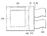
도 2는, 표시 장치(1)의 전체 구성을 도시하는 것이다. 표시 장치(1)는, 기판(13)의 중앙부에 표시 영역(110)을 갖고 있고, 예를 들면 극박형의 유기 발광 컬러 디스플레이 장치 등으로서 이용된다. 표시 영역(110)의 주변에는, 예를 들면 영상 표시용의 드라이버인 신호선 구동 회로(120), 주사선 구동 회로(130) 및 전원 공급선 구동 회로(140)가 마련되어 있다.Fig. 2 shows the entire configuration of the
표시 영역(110)에는, 매트릭스형상으로 2차원 배치된 복수의 화소(10)와, 그들을 구동하기 위한 화소 구동 회로(150)가 형성되어 있다. 하나의 화소(10)가 예를 들면 하나의 발광부(20)를 갖고 있다. 하나의 화소(10)가, 예를 들면 적색, 녹색, 청색 중 어느 하나를 발광하여도 좋고, 또는 하나의 화소(10)가 적색, 녹색 및 청색을 발광하도록 하여도 좋다. 화소 구동 회로(150)에서, 열방향(Y방향)으로는 복수의 신호선(120A)(120A1, 120A2, …, 120Am, …) 및 복수의 전원 공급선(140A)(140A1, …, 140An, …)이 배치되고, 행방향(X방향)으로는 복수의 주사선(130A)(130A1, …, 130An, …)이 배치되어 있다. 신호선(120A)과 주사선(130A)과의 교차점에, 하나의 화소(10)가 마련되어 있다. 신호선(120A)은 그 양단이 신호선 구동 회로(120)에 접속되고, 주사선(130A)은 그 양단이 주사선 구동 회로(130)에 접속되고, 전원 공급선(140A)은 그 양단이 전원 공급선 구동 회로(140)에 접속되어 있다.In the
신호선 구동 회로(120)는, 신호 공급원(도시 생략)으로부터 공급되는 휘도 정보에 응한 영상 신호의 신호 전압을, 신호선(120A)을 통하여 선택된 화소(10)에 공급하는 것이다. 주사선 구동 회로(130)는, 입력되는 클록 펄스에 동기하여 스타트 펄스를 차례로 시프트(전송)하는 시프트 레지스터 등에 의해 구성되어 있다. 주사선 구동 회로(130)는, 각 화소(10)에의 영상 신호의 기록에 즈음하여 행 단위로 그들을 주사하고, 각 주사선(130A)에 주사 신호를 순차적으로 공급하는 것이다. 신호선(120A)에는 신호선 구동 회로(120)로부터의 신호 전압이, 주사선(130A)에는 주사선 구동 회로(130)로부터의 주사 신호가 각각 공급되도록 되어 있다.The signal
전원 공급선 구동 회로(140)는, 입력되는 클록 펄스에 동기하여 스타트 펄스를 차례로 시프트(전송)하는 시프트 레지스터 등에 의해 구성되어 있다. 전원 공급선 구동 회로(140)는, 신호선 구동 회로(120)에 의한 열 단위의 주사와 동기하여, 각 전원 공급선(140A)에 대해, 각각의 양단부터, 서로 다른 제1 전위 및 제2 전위의 어느 하나를 적절히 공급한다. 이에 의해, 후술하는 구동 트랜지스터(Tr2)의 도통 상태 또는 비도통 상태의 선택이 행하여진다.The power supply
화소 구동 회로(150)는, 기판(13) 및 다층 배선층(12)에 마련되어 있다. 도 3에, 화소 구동 회로(150)의 한 구성예를 도시한다. 화소 구동 회로(150)는, 기록 트랜지스터(Tr1) 및 구동 트랜지스터(Tr2)와, 그 사이의 커패시터(유지 용량)(Cs)와, 발광부(20)를 갖는 액티브형의 구동 회로이다. 발광부(20)는, 전원 공급선(140A) 및 공통 전원 공급선(GND)의 사이에서 구동 트랜지스터(Tr2)와 직렬로 접속되어 있다. 기록 트랜지스터(Tr1) 및 구동 트랜지스터(Tr2)는, 예를 들면 실리콘 박막 트랜지스터(TFT(Thin Film Transistor))이고, 그 구성은 예를 들면 역스태거 구조(이른바 보텀 게이트형)라도 스태거 구조(톱 게이트형)라도 좋다.The
기록 트랜지스터(Tr1)는, 예를 들면 드레인 전극이 신호선(120A)과 접속되어 있고, 신호선 구동 회로(120)로부터의 영상 신호가 공급되도록 되어 있다. 또한, 기록 트랜지스터(Tr1)의 게이트 전극은 주사선(130A)과 접속되어 있고, 주사선 구동 회로(130)로부터의 주사 신호가 공급되도록 되어 있다. 또한, 기록 트랜지스터(Tr1)의 소스 전극은, 구동 트랜지스터(Tr2)의 게이트 전극과 접속되어 있다.In the writing transistor Tr1, for example, a drain electrode is connected to the
구동 트랜지스터(Tr2)는, 예를 들면 드레인 전극이 전원 공급선(140A)과 접속되어 있고, 전원 공급선 구동 회로(140)에 의한 제1 전위 또는 제2 전위의 어느 하나로 설정된다. 구동 트랜지스터(Tr2)의 소스 전극은, 발광부(20)와 접속되어 있다.The drain electrode of the driving transistor Tr2 is connected to the
유지 용량(Cs)은, 구동 트랜지스터(Tr2)의 게이트 전극(기록 트랜지스터(Tr1)의 소스 전극)과, 구동 트랜지스터(Tr2)의 드레인 전극과의 사이에 형성되는 것이다.The holding capacitor Cs is formed between the gate electrode (the source electrode of the writing transistor Tr1) of the driving transistor Tr2 and the drain electrode of the driving transistor Tr2.
[표시 장치의 주요부 구성][Main parts of display device]
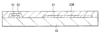
다음에, 재차 도 1을 참조하여, 기판(13), 발광부(20) 및 대향 기판(19) 등의 상세한 구성에 관해 설명한다.Next, with reference to Fig. 1 again, the detailed structure of the
기판(13)은 실리콘층(Si층)(13a)과 절연층(13b)을 포함하고, 예를 들면 Si층(13a)이 면(S1), 절연층(13b)이 면(S2)을 각각 구성하고 있다. 기판(13)을 지지하는 지지 부재(11)는, 예를 들면 실리콘에 의해 구성되어 있다. 기판(13)의 Si층(13a)에는, 기록 트랜지스터(Tr1)의 소스·드레인 영역(131a, 131b) 및 구동 트랜지스터(Tr2)의 소스·드레인 영역(132A, 132B)이 마련되어 있다. 소스·드레인 영역(131a, 131b) 및 소스·드레인 영역(132A, 132B)은, 예를 들면 Si층(13a)의 이면(기판(13)의 면(S2)과의 대향면) 부근의 N형 반도체웰 영역(이하, N형 웰 영역이라고 한다. P형 반도체 영역에 대해서도 마찬가지.)(133) 중에 마련된, P형 영역이다. Si층(13a)의 이면에는, 게이트 절연막(도시 생략)을 통하여, 기록 트랜지스터(Tr1)의 게이트 전극(TG1), 구동 트랜지스터(Tr2)의 게이트 전극(TG2)이 마련되어 있다. 게이트 전극(TG1, TG2)은, 예를 들면 백금(Pt), 티탄(Ti), 루테늄(Ru), 몰리브덴(Mo), 구리(Cu), 텅스텐(W), 니켈(Ni), 알루미늄(Al) 및 탄탈(Ta) 등의 금속 단체 또는 합금 등에 의해 구성되어 있고, 이와 같은 금속의 주위에는 절연성의 사이드-월(SW)이 마련되어 있다.The
절연층(13b)은 도전성 플러그(도전성 플러그(13W1, 13W2, 13W3, 13W4, 13W5))를 갖고 있고, 이 도전성 플러그를 통하여, 기록 트랜지스터(Tr1), 구동 트랜지스터(Tr2)와 다층 배선층(12)의 배선(배선(121, 122))이 전기적으로 접속되어 있다. 도전성 플러그(13W1, 13W2, 13W3, 13W4, 13W5)는, 절연층(13b)의 접속구멍에 마련된 도전체이다. 배선(122)은 예를 들면 도전성 플러그(13W2, 13W4)에 접속되어 있고, 이에 의해, 기록 트랜지스터(Tr1)의 소스·드레인 영역(131a)과 구동 트랜지스터(Tr2)의 게이트 전극(TG2)을 전기적으로 접속하고 있다. 구동 트랜지스터(Tr2)의 소스·드레인 영역(132B)에는 도전성 플러그(13W3)가 접속되고, 이 도전성 플러그(13W3)는 예를 들면 전원 공급선(140A)에 전기적으로 접속되어 있다. 구동 트랜지스터(Tr2)의 소스·드레인 영역(132A)은 도전성 플러그(13W5)를 통하여 배선(121)에 전기적으로 접속되어 있다. N형 웰 영역(133)의 외측에는, 기판(13) 및 절연층(14)을 관통하는 전극(관통 전극(13V))이 마련되어 있고, 이 관통 전극(13V)이 배선(121)과 발광부(20)(후술하는 제1 전극(21)), 즉 구동 트랜지스터(Tr2)의 소스·드레인 영역(132A)과 발광부(20)를 전기적으로 접속하고 있다. 관통 전극(13V)은, 예를 들면 절연층(14) 및 기판(13)을 관통하는 구멍에 폴리실리콘(Poly Si) 또는 텅스텐(W) 등의 도전재를 마련한 것이다.The insulating layer 13b has conductive plugs (conductive plugs 13W1, 13W2, 13W3, 13W4 and 13W5), and the recording transistor Tr1, the driving transistor Tr2 and the
본 실시의 형태에서는, 발광부(20)에서 발생한 광의 일부를 수광하기 위한 수광부(30)가 표시 영역(110)(도 2) 내에 마련되고, 이 수광부(30)는 기록 트랜지스터(Tr1), 구동 트랜지스터(Tr2)와 이웃하는 위치에 배치되어 있다. 상세는 후술하지만, 이에 의해 발광부(20)와 수광부(30)를 가깝게 할 수 있다. 따라서, 발광부(20)로부터 수광부(30)까지의 사이의 광량의 감소를 억제하는 것이 가능해지고, 수광부(30)의 감도를 높일 수 있다.In this embodiment, a
수광부(30)는, 예를 들면 포토 다이오드에 의해 구성되어 있고, Si층(13a)의 이면 부근의 P형 웰 영역(134) 및 P형 웰 영역(134) 중의 N형 영역(135)을 포함하고 있다. 환언하면, 수광부(30)는 기판(13)의 내부에 형성되어 있다. 이 수광부(30)는, 예를 들면 화소(10)마다 마련되어 있다. Si층(13a)의 이면에는, 게이트 절연막(도시 생략)을 통하여, 트랜지스터(Tr3)의 게이트 전극(TG3)이 마련되고, 이 트랜지스터(Tr3)에 의해 수광부(30)의 신호 전하가 플로팅 영역(FD)에 전송되도록 되어 있다. 플로팅 영역(FD)은, 예를 들면 P형 웰 영역(134) 중의 N형 영역이다. 절연층(13b)의 도전성 플러그(13W6, 13W7)는, 각각 플로팅 영역(FD), 트랜지스터(Tr3)의 게이트 전극(TG3)에, 접속되어 있다.The
이 수광부(30)는, 도 4에 도시한 바와 같이, 각 발광부(20)(화소(10))로부터의 광량의 정보(발광 정보(20D))를 검지함과 함께 외광의 광량 정보(외광 정보(LD))를 취득하고, 광전 변환한 수광 신호(30A)를 보정 회로(50)에 보내도록 되어 있다. 보정 회로(50)에서는, 이 수광 신호(30A)로부터 외광의 영향을 제거하여, 발광부(20)의 발광 상태만에 기인하는 발광 강도를 산출함과 함께 각 화소(10)의 광량에 응하여 보정 신호(50A)를 화소 구동 회로(150)에 출력한다. 화소 구동 회로(150)는, 외부로부터 입력되는 영상 신호(40A)에 이 보정 신호(50A)를 추가하여 처리를 행하고, 보정 영상 신호(41a)로서 발광부(20)(화소(10))에 출력한다. 이에 의해, 발광부(20)에 인가되는 전압 및 전류가 제어되어, 발광부(20) 사이의 휘도 얼룩이 억제된다.As shown in Fig. 4, the light-receiving
발광부(20)는, 기판(13)의 면(S1) 전면(全面)에 마련된 절연층(14)상의 소정의 영역에 배치되어 있고, 기판(13)(절연층(14))측부터, 제1 전극(21), 발광층을 포함하는 유기층(22) 및 제2 전극(23)을 이 순서로 갖고 있다.The
제1 전극(21)은 화소(10)(발광부(20))마다 마련되어 있고, 복수의 제1 전극(21)이 절연층(14)상에 서로 이간하여 배치되어 있다. 이 제1 전극(21)은 양극으로서의 기능 및 반사층으로서의 기능을 구비한 것이고, 반사율이 높고, 또한, 정공 주입성도 높은 재료에 의해 구성되어 있는 것이 바람직하다. 이와 같은 제1 전극(21)으로서는, 예를 들면, 적층 방향의 두께(이하, 단지 두께라고 말한다)가 30㎚ 이상 1000㎚ 이하이고, 크롬(Cr), 금(Au), 백금(Pt), 니켈(Ni), 구리(Cu), 몰리브덴(Mo), 텅스텐(W), 티탄(Ti), 탄탈(Ta), 알루미늄(Al) 또는 은(Ag) 등의 금속 원소의 단체 또는 합금을 들 수 있다. 제1 전극(21)은, 이와 같은 금속막을 적층하여 구성하도록 하여도 좋다. 제1 전극(21)(발광부(20))은, 기록 트랜지스터(Tr1), 구동 트랜지스터(Tr2)(기판(13)의 N형 웰 영역(133))의 바로 위에, 이것과 평면시(平面視)에서 겹쳐지도록 배치하는 것이 바람직하다. 이와 같이 제1 전극(21)을 배치함에 의해, 기록 트랜지스터(Tr1), 구동 트랜지스터(Tr2)에 입사한 외광이 제1 전극(21)에서 차단되기 때문에, 기록 트랜지스터(Tr1), 구동 트랜지스터(Tr2)의 동작점이 광에 의해 변화하는 것을 막을 수 있다.The
제1 전극(21)의 표면(제2 전극(23)과의 대향면)부터 측면은, 소자 분리층(15)으로 덮여 있고, 이 소자 분리층(15)에는 발광부(20)의 발광 영역을 규정하기 위한 개구가 마련되어 있다. 즉, 이 소자 분리층(15)의 개구에 의해 제1 전극(21)의 표면이 노출한다. 소자 분리층(15)은, 발광 영역을 정확하게 소망하는 형상으로 제어함과 함께, 제1 전극(21)과 제2 전극(23)과의 사이의 절연성 및 인접하는 발광부(20) 사이의 절연성을 확보하는 역할을 담당하고 있다. 절연층(14) 및 소자 분리층(15)에는 예를 들면, 폴리이미드 등의 유기 재료 또는 산화 실리콘(SiO2), 질화실리콘(SiNx) 및 산질화실리콘(SiON) 등의 무기 재료를 사용할 수 있다. 절연층(14)의 두께는 예를 들면 100㎚ 내지 1000㎚, 소자 분리층(15)의 두께는 예를 들면 50㎚ 내지 2500㎚이다.The side surface of the
유기층(22)은, 예를 들면, 제1 전극(21)측부터, 정공 주입층, 정공 수송층, 발광층, 전자 수송층 및 전자 주입층(모두 도시 생략)을 이 순서로 갖고 있다. 모든 발광부(20)에 공통되게 유기층(22)을 마련하도록 하여도 좋고, 또는, 발광부(20)마다 유기층(22)을 마련하도록 하여도 좋다.The
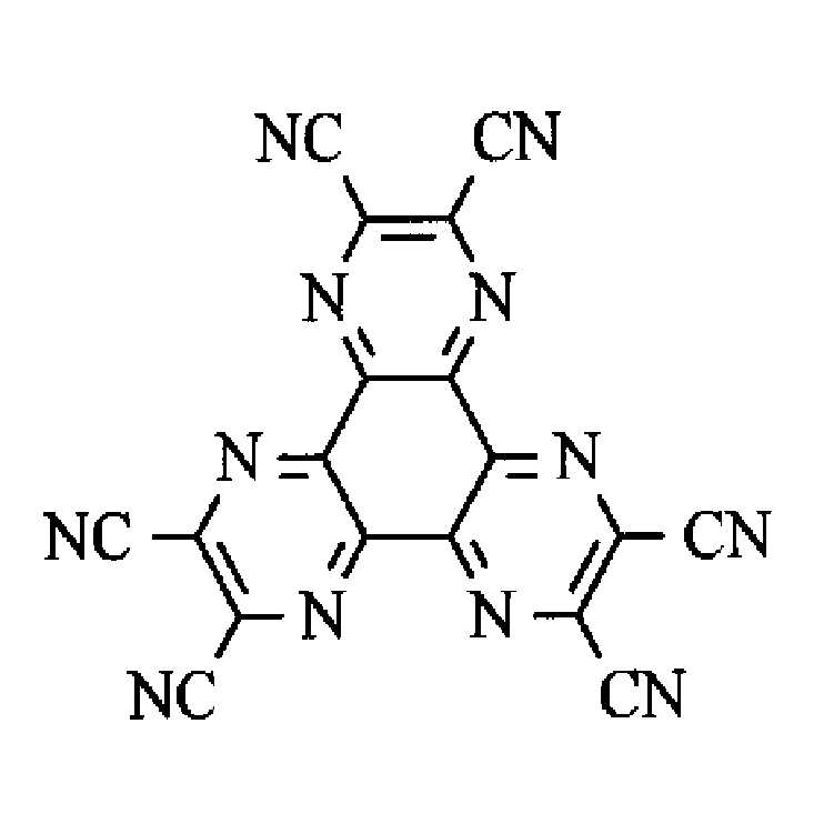
정공 주입층은, 정공 주입 효율을 높이기 위한 것임과 함께, 리크를 방지하기 위한 버퍼층이다. 정공 주입층은, 예를 들면, 두께가 1㎚ 이상 300㎚ 이하이고, 화학식 1 또는 화학식 2로 표시한 헥사아자트리페닐렌 유도체에 의해 구성되어 있다.The hole injection layer is for increasing hole injection efficiency and is a buffer layer for preventing leakage. The hole injection layer is composed of, for example, a hexaazatriphenylene derivative represented by the formula (1) or (2) with a thickness of 1 nm or more and 300 nm or less.

(화학식 1에서, R1 내지 R6 각각 독립하여, 수소, 할로겐, 하이드록실기, 아미노기, 아릴아미노기, 탄소수 20 이하의 치환 또는 무치환의 카르보닐기, 탄소수 20 이하의 치환 또는 무치환의 카르보닐에스테르기, 탄소수 20 이하의 치환 또는 무치환의 알킬기, 탄소수 20 이하의 치환 또는 무치환의 알켄일기, 탄소수 20 이하의 치환 또는 무치환의 알콕실기, 탄소수 30 이하의 치환 또는 무치환의 아릴기, 탄소수 30 이하의 치환 또는 무치환의 복소환기, 니트릴기, 시아노기, 니트로기, 또는 실릴기로부터 선택된 치환기이고, 인접하는 Rm(m=1 내지 6)은 환상 구조를 통하여 서로 결합하여도 좋다. 또한, X1 내지 X6은 각각 독립하여 탄소 또는 질소 원자이다.)A halogen atom, a hydroxyl group, an amino group, an arylamino group, a substituted or unsubstituted carbonyl group having a carbon number of 20 or less, a substituted or unsubstituted carbonyl ester group having a carbon number of 20 or less, A substituted or unsubstituted alkyl group having 20 or less carbon atoms, a substituted or unsubstituted alkenyl group having 20 or less carbon atoms, a substituted or unsubstituted alkoxyl group having 20 or less carbon atoms, a substituted or unsubstituted aryl group having 30 or less carbon atoms, A substituted or unsubstituted heterocyclic group, a nitrile group, a cyano group, a nitro group, or a silyl group, and adjacent Rm (m = 1 to 6) may be bonded to each other via a cyclic structure. To X < 6 > are each independently a carbon or nitrogen atom.
정공 수송층은, 발광층에의 정공 수송 효율을 높이기 위한 것이다. 정공 수송층은, 예를 들면, 두께가 40㎚ 정도이고, 4,4',4"-트리스(3-메틸페닐페닐아미노)트리페닐아민(m-MTDATA) 또는 α-나프틸페닐디아민(αNPD)에 의해 구성되어 있다.The hole transport layer is intended to enhance the hole transport efficiency to the light emitting layer. The hole transporting layer may be formed of, for example, a layer having a thickness of about 40 nm and doped with 4,4 ', 4 "-tris (3-methylphenylphenylamino) triphenylamine (m-MTDATA) .
발광층은 예를 들면 백색 발광용의 발광층이고, 제1 전극(21)과 제2 전극(23)과의 사이에 예를 들면 적색 발광층, 녹색 발광층 및 청색 발광층(모두 도시 생략)의 적층체를 갖고 있다. 발광부(20)마다, 적색 발광층, 녹색 발광층 및 청색 발광층의 어느 하나를 마련하도록 하여도 좋다. 적색 발광층, 녹색 발광층 및 청색 발광층은, 전계를 걸음에 의해, 제1 전극(21)으로부터 정공 주입층 및 정공 수송층을 통하여 주입된 정공의 일부와, 제2 전극(23)으로부터 전자 주입층 및 전자 수송층을 통하여 주입된 전자의 일부가 재결합하여, 각각 적색, 녹색 및 청색의 광을 발생시키는 것이다.The light emitting layer is, for example, a light emitting layer for emitting white light, and a layered body of, for example, a red light emitting layer, a green light emitting layer and a blue light emitting layer (both not shown) is provided between the
적색 발광층은, 예를 들면, 적색 발광 재료, 정공 수송성 재료, 전자 수송성 재료 및 양 전하 수송성 재료 중 적어도 1종을 포함하고 있다. 적색 발광 재료는, 형광성의 것이라도 인광성의 것이라도 좋다. 적색 발광층은, 예를 들면, 두께가 5㎚ 정도이고, 4,4-비스(2,2-디페닐비닐)비페닐(DPVBi)에 2,6-비스[(4'-메톡시 디페닐아미노)스티릴]-1,5-디시아노나프탈렌(BSN)을 30중량% 혼합한 것에 의해 구성되어 있다.The red luminescent layer includes, for example, at least one of a red light emitting material, a hole transporting material, an electron transporting material, and a positive charge transporting material. The red luminescent material may be either fluorescent or phosphorescent. The red luminescent layer is, for example, a layer having a thickness of about 5 nm and doped with 4,4-bis (2,2-diphenylvinyl) biphenyl DPVBi with 2,6-bis [(4'-methoxy diphenylamino ) Styryl] -1,5-dicyanonaphthalene (BSN) in an amount of 30% by weight.
녹색 발광층은, 예를 들면, 녹색 발광 재료, 정공 수송성 재료, 전자 수송성 재료 및 양 전하 수송성 재료 중 적어도 1종을 포함하고 있다. 녹색 발광 재료는, 형광성의 것이라도 인광성의 것이라도 좋다. 녹색 발광층은, 예를 들면, 두께가 10㎚ 정도이고, DPVBi에 쿠마린6을 5중량% 혼합한 것에 의해 구성되어 있다.The green light emitting layer includes at least one of, for example, a green light emitting material, a hole transporting material, an electron transporting material, and a positive charge transporting material. The green light emitting material may be either a fluorescent or a phosphorescent material. The green luminescent layer is formed by, for example, having a thickness of about 10 nm and mixing DPVBi with coumarin 6 in an amount of 5% by weight.
청색 발광층은, 예를 들면, 청색 발광 재료, 정공 수송성 재료, 전자 수송성 재료 및 양 전하 수송성 재료 중 적어도 1종을 포함하고 있다. 청색 발광 재료는, 형광성의 것이라도 인광성의 것이라도 좋다. 청색 발광층은, 예를 들면, 두께가 30㎚ 정도이고, DPVBi에 4,4'-비스[2-{4-(N,N-디페닐아미노)페닐}비닐]비페닐(DPAVBi)을 2.5중량% 혼합한 것에 의해 구성되어 있다.The blue light emitting layer includes at least one of, for example, a blue light emitting material, a hole transporting material, an electron transporting material, and a positive charge transporting material. The blue luminescent material may be either fluorescent or phosphorescent. The blue luminescent layer is, for example, a layer having a thickness of about 30 nm and doped with DPVBi in an amount of 2.5 wt% of 4,4'-bis [2- {4- (N, N-diphenylamino) phenyl} %.
전자 수송층은, 발광층에의 전자 수송 효율을 높이기 위한 것이고, 예를 들면 두께가 20㎚ 정도의 8-히드록시퀴놀린알루미늄(Alq3)에 의해 구성되어 있다. 전자 주입층은, 발광층에의 전자 주입 효율을 높이기 위한 것이고, 예를 들면 두께가 0.3㎚ 정도의 LiF 또는 Li2O 등에 의해 구성되어 있다.The electron transporting layer is for increasing the electron transport efficiency to the light emitting layer, and is made of, for example, 8-hydroxyquinoline aluminum (Alq3) having a thickness of about 20 nm. The electron injection layer is for increasing electron injection efficiency into the light emitting layer, and is made of, for example, LiF or Li 2 O with a thickness of about 0.3 nm.
제2 전극(23)은, 유기층(22)을 사이에 두고 제1 전극(21)과 쌍(對)을 이루고, 제1 전극(21)과 절연된 상태에서 예를 들면 전자 주입층의 위에 발광부(20)(화소(10))에 공통되게 마련되어 있다. 제2 전극(23)은, 광투과성의 투명 재료로 이루어지고, 예를 들면, 알루미늄(Al), 마그네슘(Mg), 은(Ag), 칼슘(Ca) 또는 나트륨(Na)의 합금에 의해 구성되어 있다. 그 중에서도, 마그네슘과 은과의 합금(Mg-Ag 합금)은, 박막에서의 도전성과 흡수의 작음을 겸비하고 있기 때문에 바람직하다. Mg-Ag 합금에서의 마그네슘과 은과의 비율은 특히 한정되지 않지만, 막두께비로 Mg:Ag=20:1 내지 1:1의 범위인 것이 바람직하다. 또한, 제2 전극(23)의 재료에는, 알루미늄(Al)과 리튬(Li)과의 합금(Al-Li 합금)을 사용하도록 하여도 좋고, 인듐주석 산화물(ITO), 산화아연(ZnO), 알루미나 도프 산화아연(AZO), 갈륨 도프 산화아연(GZO), 인듐아연 산화물(IZO), 인듐티탄 산화물(ITiO) 또는 인듐텅스텐 산화물(IWO) 등을 사용하여도 좋다.The
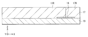
보호층(16)은, 제2 전극(23)을 덮도록 기판(13)의 전면에 마련되고, 예를 들면, 폴리이미드 등의 절연성 수지 재료에 의해 구성되어 있다. 대향 기판(19)의 일방의 면(기판(13)과의 대향면)에 마련된 CF층(17)은, 적색 컬러 필터(17R), 녹색 컬러 필터(도시 생략) 및 청색 컬러 필터(17b)를 갖고 있고, 이들이 각각의 발광부(20)(화소(10))에 대응하여 차례로 배치되어 있다. CF층(17)은, 대향 기판(19)의 어느 측의 면에 마련되어도 좋지만, 발광부(20)의 측에 마련되는 것이 바람직하다. 컬러 필터가 표면에 노출하지 않고, 보호층(16)(또는 접착층)에 의해 보호될 수 있기 때문이다. 또한, 유기층(22)과 컬러 필터와의 사이의 거리가 좁아짐에 의해, 유기층(22)에서 출사한 광이 인접하는 다른 색의 컬러 필터에 입사하여 혼색이 생기는 것을 피할 수 있기 때문이다.The
반사부(18)는, 발광부(20)에서 발생한 광 중, 대향 기판(19)을 향하는 광을 반사하여 기판(13) 내의 수광부(30)에 모으기 위한 것이고, 예를 들면 수광부(30)와 대향하는 영역에 화소(10)마다 마련되어 있다. 이 반사부(18)로는 예를 들면 알루미늄, 텅스텐, 은 또는 티탄 등의 반사율이 높은 금속막을 이용할 수 있다. 이와 같은 금속에, 질화티탄(TiN) 등의 질화물 또는 산화물을 적층하여 반사부(18)를 구성하도록 하여도 좋다. 예를 들면, 대향 기판(19)측부터, 질화티탄 및 알루미늄을 적층시킨 반사부(18)는, 표시면측에서의 반사를 억제함과 함께, 발광부(20)로부터의 광을 효율적으로 반사시켜서 수광부(30)에 입사시킬 수 있다. 반사부(18)와 함께, 이웃하는 화소(10) 사이에서의 광 누설을 방지하기 위한 차광부(도시 생략)를 마련하도록 하여도 좋고, 예를 들면 알루미늄으로 이루어지는 반사부(18)와 질화티탄으로 이루어지는 차광부를 적층하도록 하여도 좋다. 대향 기판(19)은, 열경화형 수지 등의 접착층(도시 생략) 등와 함께 발광부(20)를 밀봉하는 것이고, 유기층(22)에서 발생한 광을 투과하는 투명한 유리 또는 플라스틱 재료에 의해 구성되어 있다.The
[표시 장치의 제조 방법][Manufacturing method of display device]
이와 같은 표시 장치(1)는, 예를 들면 다음과 같이 하여 제조할 수 있다(도 5a 내지 도 6b).Such a
우선, 기판(13)을 형성한다. 구체적으로는, 최초에, Si층(13a)의 일방의 면의 부근에 예를 들면 이온 주입에 의해 N형 웰 영역(133), 기록 트랜지스터(Tr1)의 소스·드레인 영역(131a, 131b), 구동 트랜지스터(Tr2)의 소스·드레인 영역(132A, 132B), P형 웰 영역(134), N형 영역(135), 플로팅 영역(FD)을 형성한다(도 5a). Si층(13a)으로는, 예를 들면, SOI(Silicon On Insulator) 기판을 이용할 수 있다. 뒤이어, 상기 불순물 확산 영역을 마련한 Si층(13a)의 면상에 게이트 절연막(도시 생략)을 통하여 기록 트랜지스터(Tr1), 구동 트랜지스터(Tr2), 트랜지스터(Tr3)의 게이트 전극(TG1, TG2, TG3)을 형성한다. 이 게이트 전극(TG1, TG2, TG3)은, 도전막을 예를 들면 CVD(Chemical Vapor Deposition)법에 의해 성막한 후, 이것을 드라이 에칭함에 의해 형성할 수 있다. 이 후, 게이트 전극(TG1, TG2, TG3)을 덮도록 절연층(13b)을 성막한다. 이에 의해 기판(13)이 형성된다. 이 때, 절연층(13b)에는 도전성 플러그(13W1, 13W2, 13W3, 13W4, 13W5, 13W6, 13W7)를 마련하여 둔다. 기판(13)을 형성한 후, 기판(13)의 절연층(13b)상(기판(13)의 면(S2)상)에 다층 배선층(12)(배선(121), 배선(122))을 형성한다(도 5b).First, the
계속해서, 이 다층 배선층(12)에 지지 부재(11)(도 1)를 접합한 후, 지지 부재(11), 다층 배선층(12) 및 기판(13)을 반전하고, Si층(13a)의 타방의 면(N형 웰 영역(133) 및 P형 웰 영역(134) 등의 형성면과는 반대측의 면)측에서 Si층(13a)이 소망하는 두께가 되도록, 예를 들면 CMP(Chemical Mechanical Polishing)에 의해 연마한다(도 5c). 이 연마된 면이 기판(13)의 면(S1)이 된다. 예를 들면 CMP 공정 전에 그라인더에 의한 황(荒)연마, CMP 공정 후에 핫 인산 등의 약액을 이용한 Si층(13a)의 평탄화를 행한다. Si층(13a)의 연마는, 뒤이어, 이 기판(13)의 면(S1)상에 절연층(14)을 성막한 후, 관통 전극(13V)을 형성한다. 관통 전극(13V)은, 예를 들면 절연층(14) 및 기판(13)을 관통하는 구멍을 마련한 후, 이 구멍에 도전 재료를 매입하고, CMP를 행하여 형성한다.Subsequently, after the supporting member 11 (Fig. 1) is bonded to the
이어서, 절연층(14)상에 예를 들면 알루미늄을 스퍼터법에 의해 성막한 후, 이것을 포토 리소그래피 공정을 이용하여 패터닝하고, 제1 전극(21)을 형성한다. 계속해서, 제1 전극(21) 및 절연층(14)상에 예를 들면 플라즈마 CVD법에 의해 예를 들면 질화실리콘막을 성막한 후, 이 질화실리콘막에 개구를 마련하여 소자 분리층(15)을 형성한다. 소자 분리층(15)의 형성에 STI(Shallow trench isolation)를 이용하도록 하여도 좋다.Subsequently, for example, aluminum is deposited on the insulating
소자 분리층(15)을 마련한 후, 예를 들면 증착법에 의해 발광층을 포함하는 유기층(22) 및 제2 전극 13을 형성한다(도 5d). 이와 같이 하여 발광부(20)를 마련한 후, 예를 들면 CVD법 또는 스퍼터법에 의해, 발광부(20)의 위에 보호층(16)을 형성한다.After the
한편, 대향 기판(19)의 표면에는 반사부(18) 및 CF층(17)을 예를 들면 이 순서로 형성한다(도 6a, 도 6b). 이 후, CF층(17)을 마련한 대향 기판(19)의 주연에 실제를 도포하고, 이것을 보호층(16)을 마련한 기판(13)과 접합한다. 최후에, 기판(13)과 대향 기판(19)과의 사이의 간극에 충전제를 주입한 후, 이것을 밀봉하여 표시 장치(1)를 완성시킨다.On the other hand, on the surface of the
[표시 장치의 동작][Operation of display apparatus]
이 표시 장치(1)에서는, 각 화소(10)에 대해 주사선 구동 회로(130)로부터 기록 트랜지스터(Tr1)의 게이트 전극(TG1)을 통하여 주사 신호가 공급됨과 함께, 신호선 구동 회로(120)로부터 화상 신호가 기록 트랜지스터(Tr1)를 통하여 유지 용량(Cs)에 유지된다. 즉, 이 유지 용량(Cs)에 유지된 신호에 응하여 구동 트랜지스터(Tr2)가 온 오프 제어되고, 이에 의해, 각 발광부(20)에 구동 전류(Id)가 주입됨에 의해, 정공과 전자가 재결합하여 발광이 일어난다. 도 7에 도시한 바와 같이, 이 광(광(L1))은, 제2 전극(23), CF층(17) 및 대향 기판(19)을 투과하여 취출된다.In this
한편, 발광부(20)에서 발생한 광의 일부(광(L2))는, 반사부(18)에서 반사되어, 기판(13)의 수광부(30)에 입사한다. 이 수광부(30)로부터의 수광 신호(30A)(도 4)를 받아, 보정 회로(50)는 예를 들면 이하와 같이 하여 보정 신호(50A)를 화소 구동 회로(150)에 보낸다(도 8). 우선, 발광부(20)의 소광시, 점등시에 각각 수광부(30)를 구동하여, 외광 정보(LD) 및 발광 정보(20D)를 취득한다. 수광부(30)의 구동 전에는, 수광부(30)를 초기화하여 둔다. 이 수광부(30)에서 검지된 외광 정보(LD) 및 발광 정보(20D)는 ADC(Analog to Digital Converter)에서 디지털 변환된 후, 보존된다. 이 디지털 변환 및 보존할 때에는, 예를 들면 발광부(20)는 소등하고 있다. 보정 회로(50)에서는, 발광 정보(20D)의 디지털 데이터로부터 외광 정보(LD)의 디지털 데이터를 감산함에 의해, 발광부(20)만에 기인한 각 화소(10)의 발광 강도를 산출한 후, 각 화소(10)의 발광 상태와 대상 화소의 발광 상태를 비교하여 각 화소(10)의 휘도에 응한 보정 신호(50A)를 생성한다. 예를 들면 이 타이밍에서 보정 회로(50)는 새로운 보정 정보로 갱신된다. 화소 구동 회로(150)는, DAC(Digital to Analog Converter)에서 변환한 영상 신호(40A)에 보정 신호(50A)를 추가하여, 보정 영상 신호(41a)를 발광부(20)에 보낸다. 이와 같은 보정 신호(50A)의 취득과 영상 출력은 연속하지 않아도 좋다. 예를 들면 영상 출력 60프레임에 한 번, 보정 신호(50A)를 취득하도록 하여도 좋고, 또는 전원의 온, 오프시에 보정 신호(50A)를 취득하도록 하여도 좋다. 발광부(20) 및 보정 회로(50)의 동작은, 보정 정보의 갱신의 타이밍에 의해 적절히 변경하는 것이 가능하다. 외광 정보(LD) 및 발광 정보(20D)의 광량이 수광부(30)의 수광량을 초과하는 경우에 에러가 되도록 설정하여도 좋고, 또는, 재차 수광하도록 설정하여 두어도 좋다. 또한, ADC 및 DAC는 보정 회로(50)에 포함되어 있어도 좋고, 보정 회로(50)의 외부에 마련하도록 하여도 좋다.On the other hand, a part (light L2) of light generated in the
[표시 장치의 작용·효과][Function and effect of display device]
여기서는, 표시 영역(110) 내에 수광부(30)가 마련되어 있기 때문에, 발광부(20)와 수광부(30)와의 거리를 짧게 하여, 발광부(20)로부터의 광을 감도(感度) 좋고, 정확하게 검지할 수 있다. 따라서, 보다 효과적으로 휘도 얼룩을 억제할 수 있다. 이하, 이에 관해 설명한다.The distance between the
도 9는 비교예에 관한 표시 장치(표시 장치(100))의 평면 구성을 모식적으로 도시한 것이다. 이 표시 장치(100)의 수광부(300)는 표시 영역(110)의 외측의 영역에 배치되어 있다. 이 때문에, 각각의 화소(10)(발광부)와 수광부(300) 사이의 거리가 길어져 버린다. 또한, 각 화소에 따라 수광부(300)와 사이의 거리가 다르기 때문에, 보정 회로에서는 발광부의 열화에 더하여, 각 화소와 수광부(300) 사이의 거리에 의한 광의 감쇠를 고려하여야 한다.Fig. 9 schematically shows a planar configuration of a display device (display device 100) according to a comparative example. The
휘도 얼룩을 억제하는 방법으로서, 표시 장치의 영상을 외부의 촬상 장치에 받아들이는 방법도 제안되어 있다(예를 들면, 특개2011-77825호 공보 참조). 그러나, 이 방법에서는, 영상의 받아들임의 정밀도가 조작자에 의해 좌우되기 때문에, 발광부로부터의 광을 정확하게 검지할 수가 없다. 이 밖에, 복수의 트랜지스터와 용량 소자를 조합시킴에 의해, 화소를 구동하기 위한 트랜지스터의 성능의 편차를 조정하는 것도 가능하다(예를 들면, 특개2010-145579호 공보 참조). 그러나 이 방법에서는, 발광부의 열화에 수반하는 각 화소 사이의 휘도 얼룩을 보정할 수가 없다. 또한, 화소의 피치가 미세화하면, 용량 소자의 면적이 작아지기 때문에, 충분한 용량을 얻는 것이 곤란해진다.As a method for suppressing luminance unevenness, a method of receiving an image of a display device into an external imaging device has also been proposed (see, for example, Japanese Unexamined Patent Publication No. 2011-77825). However, in this method, since the precision of the acceptance of the image is influenced by the operator, the light from the light emitting portion can not be accurately detected. In addition, by combining a plurality of transistors and a capacitor, it is also possible to adjust the deviation of the performance of the transistor for driving the pixel (see, for example, Japanese Patent Laid-Open No. 2010-145579). However, this method can not correct luminance unevenness between pixels due to deterioration of the light emitting portion. Further, if the pixel pitch is made finer, the area of the capacitor element becomes smaller, and it becomes difficult to obtain a sufficient capacity.
이에 대해 표시 장치(1)에서는, 표시 영역(110)(도 2) 내에 수광부(30)가 마련되어 있기 때문에, 각 발광부(20)(화소(10))마다 기판(13)의 내부에 수광부(30)를 배치하여, 발광부(20)와 수광부(30) 사이의 거리를 가깝게 하는 것이 가능해진다. 발광부(20)는, 발광부(20)를 구동하기 위한 트랜지스터(기록 트랜지스터(Tr1), 구동 트랜지스터(Tr2))의 바로 위에 마련되고, 수광부(30)는, 예를 들면 이 트랜지스터와 이웃하는 위치에 화소(10)마다 배치된다. 따라서, 기판(13)의 면내 방향(XY평면)에서의 발광부(20)와 수광부(30)와의 거리가 짧아지고, 예를 들면 마이크로 OLED(Organic Light Emitting Diode) 등의 화소 피치가 작은 디스플레이에도 적용하는 것이 가능해진다.In this regard, in the
도 10에 도시한 바와 같이, 기판(13)의 면(S1)상에 다층 배선층(다층 배선층(212))을 마련하는 것도 가능하지만, 이와 같은 구성에서는, 기판(13)의 면(면(S1, S2))에 대해 수직 방향(Z방향의 거리)에서의 발광부(20)와 수광부(30)와의 거리가 멀어져 버린다. 또한, 다층 배선층(212) 중에 발광부(20)로부터의 광을 수광부(30)에 유도하기 위한 도파로 구조가 필요해진다. 이 때문에, 기판(13)의 표면(면(S1))에 발광부(20), 이면(면(S2))에 다층 배선층(12)을 각각 마련하고, 기판(13)의 면에 대해 수직 방향에서의 발광부(20)와 수광부(30)와의 거리도 좁히는 것이 바람직하다.It is also possible to provide a multilayer wiring layer (multilayer wiring layer 212) on the surface S1 of the
이상과 같이 본 실시의 형태의 표시 장치(1)에서는, 표시 영역(110) 내에 수광부(30)를 마련하도록 하였기 때문에, 발광부(20)와 수광부(30) 사이의 거리를 작게 할 수 있다. 즉, 발광부(20)와 수광부(30) 사이에서의 광량의 감소를 억제하는 것이 가능해지고, 수광부(30)는 보다 정확하게 수광 신호(30A)를 보정 회로(50)에 보낼 수 있다. 따라서, 표시 영역(110) 내에서의 각 화소(10) 사이의 휘도 얼룩을 억제할 수 있다.As described above, in the
이하, 상기 실시의 형태의 변형예 및 다른 실시의 형태에 관해 설명하지만, 이후의 설명에 있어서 상기 실시의 형태와 동일 구성 부분에 관해서는 동일 부호를 붙이고 그 설명은 적절히 생략한다.Modifications of the above embodiment and other embodiments will be described below. In the following description, the same constituent elements as those of the above embodiment will be denoted by the same reference numerals and the description thereof will be omitted as appropriate.
<변형예 1>≪ Modification Example 1 &
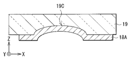
도 11은, 변형예 1에 관한 표시 장치(표시 장치(1a))의 단면 구성을 도시한 것이다. 이 표시 장치(1a)의 반사부(반사부(18a))는 이른바 파라볼라 형상이고, 기판(13)에 대향하여 포물곡면을 갖고 있다. 이 점을 제외하고, 표시 장치(1a)는 표시 장치(1)와 같은 구성을 가지며, 그 작용 및 효과도 마찬가지이다.11 shows a sectional configuration of a display device (display device 1a) according to a first modified example. The reflecting portion (reflecting portion 18a) of the display device 1a has a so-called parabola shape and has a parabolic curved surface facing the
반사부(18a)의 포물곡면은 수광부(30)에 초점을 갖는 것이고, 도 12에 도시한 바와 같이, 발광부(20)로부터 반사부(18a)를 향한 광(광(L2))은, 반사부(18a)로부터 수광부(30)에 효율적으로 집광된다. 따라서, 발광부(20)로부터 반사부(18a)에 의해 수광부(30)에 입사하는 광의 광량을 늘려서, 보다 높은 정밀도로 각 화소(10)의 휘도를 보정하는 것이 가능해진다.12, the light (light L2) directed from the
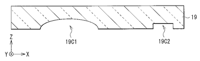
반사부(18a)는, 예를 들면 이하와 같이 하여 형성할 수 있다. 우선, 대향 기판(19) 중, 반사부(18a)의 형성 예정 영역에 포물곡면을 갖는 오목부(19C)를 형성한다(도 13). 구체적으로는, 대향 기판(19)의 표면에 레지스트를 마련한 후, 예를 들면 포토 리소그래피 공정에 의해 노광량을 조정하여 레지스트에 포물곡면을 형성한다. 즉, 레지스트를 중심부가 얇고, 또한, 주위를 두껍게 한 형상으로 성형한다. 이 레지스트의 포물곡면은 하프톤 마스크를 이용하여 형성하여도 좋고, 또는 리플로 공정에 의해 형성하는 것도 가능하다. 이 포물곡면을 갖는 레지스트를 이용하여 예를 들면 플라즈마 에칭을 행함에 의해, 대향 기판(19)에 오목부(19C)가 형성된다. 오목부(19C)를 마련한 후, 대향 기판(19)의 전면에 예를 들면 반사율이 높은 금속막을 성막한 후, 반사부(18a)의 형성 예정 영역에 레지스트로 마스크를 형성하여 플라즈마 에칭 또는 웨트 에칭을 행한다. 최후에 레지스트를 제거하고 반사부(18a)를 형성한다. 도 14에 도시한 바와 같이, 대향 기판(19)의 사각형상의 오목부(19C)에 금속막을 성막한 후, 예를 들면 CMP 등에 의해 이 금속막을 삭제하여 반사부(18a)를 형성하는 것도 가능하다. 반사부(18a)를 형성할 때에는, 대향 기판(19)에, 반사부(18a)가 마련된 오목부(19C1)와 함께 반사부(18a)의 얼라인먼트용의 오목부(19C2)를 마련하여 두는 것이 바람직하다(도 15).The reflection portion 18a can be formed, for example, as follows. First, a
<제2의 실시의 형태>≪ Second Embodiment >
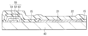
도 16은, 제2의 실시의 형태에 관한 표시 장치(표시 장치(2))의 단면 구성을 도시한 것이다. 이 표시 장치(2)는, 기록 트랜지스터(Tr1), 구동 트랜지스터(Tr2)와 수광부(30)와의 사이에 차폐부(차폐부(31))를 갖는 것이다. 이 점을 제외하고, 표시 장치(2)는 표시 장치(1)와 같은 구성을 가지며, 그 작용 및 효과도 마찬가지이다.Fig. 16 shows a sectional configuration of a display device (display device 2) according to the second embodiment. This
차폐부(31)는, 예를 들면 Si층(13a)의 홈에 마련한 실리콘산화막 및 실리콘질화막 등의 절연막 또는 텅스텐, 티탄 및 질화티탄 등의 금속막이다. 절연막 및 금속막을 겹쳐서 차폐부(31)를 구성하도록 하여도 좋고, 예를 들면 Si층(13a)의 홈에 실리콘산화막, 실리콘질화막, 티탄 또는 질화티탄 및 텅스텐을 이 순서로 적층하도록 하여도 좋다. Si층(13a)의 홈은, 기록 트랜지스터(Tr1), 구동 트랜지스터(Tr2) 및 수광부(30)의 형성 영역의 깊이까지 마련되어 있으면 좋지만(도 16), Si층(13a)을 관통하고 있어도 좋다(도 17a). 차폐부(31)의 형상은, 테이퍼형상(도 16)이라도 좋고, 주상(도 17b)이라도 좋다. 차폐부(31)는, 기록 트랜지스터(Tr1), 구동 트랜지스터(Tr2)가 마련된 N형 웰 영역(133)과 수광부(30)가 마련된 P형 웰 영역(134)과의 사이에 배치되어 있고, 수광부(30)(P형 웰 영역(134))을 둘러싸고 있다(도 18a, 도 18b). 차폐부(31)는 N형 웰 영역(133)을 둘러싸도록 하여도 좋고(도 18c), 또는 P형 웰 영역(134) 및 N형 웰 영역(133)을 둘러싸고 있어도 좋다(도 18d).The shielding
이와 같은 차폐부(31)를 마련함에 의해, 보다 정확하게 발광부(20)로부터의 광을 수광부(30)에서 검지할 수 있다. 이하, 이에 관해 상세히 설명한다. 도 19에 도시한 바와 같이, 발광부(20)에서 광이 발생함에 의해, 기판(13)(Si층(13a))의 온도가 상승하고, 잉여 캐리어(캐리어(C))가 발생한다. 반사부(18)에서 반사되어 기판(13)에 입사한 광 중, 수광부(30) 이외의 부분에 입사한 광도 이와 같은 캐리어(C)의 발생 원인이 된다. 차폐부(31)는, 이와 같은 수광부(30)의 외측에서 발생한 캐리어(C)가 수광부(30) 내로 침입하는 것을 막기 위한 것이다. 즉, 차폐부(31)를 마련함에 의해, 캐리어(C)의 수광부(30)로의 침입이 차단되어, 보다 정확하게 각 발광부(20)로부터의 광을 수광부(30)가 검지한다.By providing such a
차폐부(31)는, 예를 들면, 도 20에 도시한 바와 같이, Si층(13a)에 수광부(30)(P웰 영역(134) 및 N형 영역(135)) 및 플로팅 영역(FD)을 마련한 후, 예를 들면 수광부(30)의 주위에 홈을 형성하고, 이 홈에 절연막을 매입하여 형성한다. 절연막을 매입한 후, 예를 들면 CMP 등에 의해 연마하도록 하여도 좋다. 차폐부(31)는, 예를 들면 기판(13)과 대향 기판(19)과의 위치맞춤을 행하기 위한 마크(예를 들면 BSA(Back Side Alig㎚ent))와 함께 형성하는 것도 가능하다. 또는, Si층(13a)을 연마한 후(도 5c), 관통 전극(13V)과 함께 상기 절연막 또는 금속막으로 이루어지는 차폐부(31)를 형성하도록 하여도 좋다. 관통 전극(13V)과 함께 차폐부(31)를 형성함으로써, 에칭 가공 공정을 단순화할 수 있다.20, the shielding
<변형예 2>≪ Modification Example 2 &
도 21에 도시한 바와 같이, 수광부(30)의 주위에 예를 들면, 구리, 텅스텐 및 알루미늄 등의 차광성이 높은 금속막을 포함하는 차폐부(차폐부(32))를 마련하도록 하여도 좋다(변형예 2). 이 차폐부(32)를 갖는 표시 장치(2A)에서는, 수광부(30)로부터 이웃하는 화소(10) 및 기록 트랜지스터(Tr1), 구동 트랜지스터(Tr2)의 형성 영역으로의 광의 누출이 억제되고, 수광부(30)에 발광부(20)로부터의 광을 보다 효율 좋게 모을 수 있다. 차폐부(32)는, 상기 제2의 실시의 형태의 차폐부(31)와 마찬가지로, Si층(13a)의 홈에 마련되어 있고, 이 홈에 예를 들면 절연막 및 금속막을 이 순서로 매입하여 형성한다. 이 절연막으로는, 예를 들면 실리콘산화막 또는 실리콘질화막 등을 이용하는 것이 가능하다.A shielding portion (shielding portion 32) including a metal film with high light shielding property such as copper, tungsten, and aluminum may be provided around the
<제3의 실시의 형태>≪ Third Embodiment >
도 22는, 제3의 실시의 형태에 관한 표시 장치(표시 장치(3))의 주요부의 단면 구성을 도시한 것이다. 이 표시 장치(3)에서는, 기판(기판(43))의 표면에 발광부(20)와 함께 수광부(수광부(50))가 마련되어 있다. 이 점을 제외하고, 표시 장치(3)는 표시 장치(1)와 같은 구성을 가지며, 그 작용 및 효과도 마찬가지이다. 도 22에서는, 보호층(16), CF층(17) 및 대향 기판(19)(도 1 등)을 생략하였다.22 shows a sectional configuration of a main part of a display device (display device 3) according to the third embodiment. In this
기판(43)은, 예를 들면 판형상 부재(43a)에 TFT층(43b)을 적층함에 의해 구성되어 있고, TFT층(43b)상에 발광부(20) 및 수광부(50)가 마련되어 있다. 판형상 부재(43a)는, 예를 들면, 석영, 유리, 실리콘(Si), 금속박, 또는 수지제의 필름이나 시트 등에 의해 구성되어 있다. TFT층(43b)에는, 발광부(20)를 구동하기 위한 트랜지스터, 예를 들면 기록 트랜지스터(Tr1) 및 구동 트랜지스터(Tr2)(도 3)가 마련되어 있다. TFT층(43b)에는, 발광부(20) 및 수광부(50)에 접속된 배선도 마련되어 있다.The
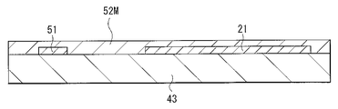
수광부(50)는, 평면시에서 발광부(20)와 이웃하는 위치에, 예를 들면, 화소(10)(도 2)마다 배치되어 있다. 이 수광부(50)는 기판(43)측부터, 하부 전극(51), 광전 변환막(52) 및 상부 전극(53)을 갖는 것이고, 발광부(20)로부터의 광을 받아서 신호 전하(예를 들면 전자)를 생성한다. 이 신호 전하는, 하부 전극(51)으부터 취출되고, 수광 신호(30A)로서 보정 회로(50)에 보내지도록 되어 있다(도 4). 하부 전극(51), 광전 변환막(52) 및 상부 전극(53)은, 수광부(50)마다 패터닝되어 있다.The
하부 전극(51)은, 예를 들면 발광부(20)의 제1 전극(21)과 동층에 마련되어 있고, 예를 들면 TFT층(43b)의 배선을 통하여 보정 회로(50)(도 4)에 전기적으로 접속되어 있다. 이 하부 전극(51)에는, 제1 전극(21)과 같은 재료, 예를 들면 알루미늄을 이용할 수 있다. 광전 변환막(52)은, 발광부(20)에서 발생한 파장의 광(가시광)을 흡수하고, 전자·홀 쌍을 발생시키는 것이고, 예를 들면, CIGS(Copper Indium Gallium Selenide) 또는 유기 광전 변환 재료 등에 의해 구성되어 있다. 상부 전극(53)은, 이 광전 변환막(52)에서 발생한 전자·홀 쌍의 한쪽(예를 들면 홀)을 배출하기 위한 것이고, 예를 들면, TFT층(43b)의 배선을 통해 GND에 전기적으로 접속되어 있다. 상부 전극(53)에는, 예를 들면 발광부(20)의 제2 전극(23)과 같은 광투과성 도전 재료를 사용할 수 있다. 이 상부 전극(53)은 소자 분리층(15)에 덮여 있고, 또한 이 소자 분리층(15)은 발광부(20)로부터 연재된 유기층(22) 및 제2 전극(23)에 의해 덮여 있다. 표시 장치(1)와 마찬가지로, 수광부(50)와 대향하는 위치에 반사부(18)를 마련하도록 하여도 좋다(도 1).The
이와 같은 표시 장치(3)는, 예를 들면 이하와 같이 하여 제조할 수 있다(도 23a 내지 도 25c).Such a
우선, 기판(43)의 표면 전면에 예를 들면 스퍼터법에 의해 도전막(51M)을 성막한 후(도 23a), 이것을 드라이 에칭 또는 웨트 에칭에 의해 패터닝하여, 하부 전극(51)을 형성한다(도 23b). 도전막(51M)으로부터, 하부 전극(51)과 함께 제1 전극(21)을 형성하도록 하여도 좋다.First, a
뒤이어, 기판(43)의 전면에 광전 변환막(52M)을 예를 들면 스퍼터링법에 의해 성막한 후(도 23c), 이것을 패터닝하여 하부 전극(51)의 윗면 및 측면을 덮는 광전 변환막(52)을 형성한다(도 24a). 계속해서, 예를 들면 기판(43)의 전면에 광투과성의 도전막(53M)을 성막한 후(도 24b), 이 도전막(53M)을 패터닝하여 광전 변환막(52)상에 상부 전극(53)을 형성한다(도 24c). 상부 전극(53)은, 예를 들면 광전 변환막(52)의 윗면 및 측면을 덮고 있다. 이에 의해, 수광부(50)가 형성된다. 수광부(50)를 마련한 후, 기판(43)의 전면에 절연막(15M)을 성막한다(도 25a). 이 절연막(15M)의 일부에 개구를 마련하여 제1 전극(21)의 표면을 노출시켜서, 소자 분리층(15)을 형성한다(도 25b). 소자 분리층(15)을 마련한 후, 기판(43)의 전면에 유기층(22) 및 제2 전극(23)을 이 순서로 성막하고, 발광부(20)를 형성한다(도 25c). 이후의 공정은 표시 장치(1)와 마찬가지로 행하여, 표시 장치(3)를 완성시킨다.Subsequently, a
이 표시 장치(3)의 수광부(50)는, 표시 장치(1)의 수광부(30)(도 1, 도 7)와 마찬가지로 하여 발광부(20)에서 발생한 광의 일부를 수광한다. 기판(43)의 표면의 수광부(50)는, 기판(13)의 내부의 수광부(30)보다도 발광부(20)에 보다 가까운 위치에 마련되어 있기 때문에, 반사부(18)를 이용하지 않고서, 발광부(20)에서 발생한 광을 직접 받는 것이 가능해진다. 따라서, 발광부(20)로부터 수광부(50)까지 사이의 광량의 감소를 억제하여, 보다 정확한 수광 신호(30A)를 보정 회로(50)에 보내는 것이 가능해진다.The
(모듈)(module)
상기 실시의 형태 및 변형예의 표시 장치(1, 1a, 2, 2A, 3)(이하, 단지 표시 장치로 표시한다)는, 예를 들면, 도 26에 도시한 바와 같은 모듈로서, 후술하는 적용예 1 내지 5 등의 여러가지의 전자 기기에 조립된다. 이 모듈은, 예를 들면, 기판(13, 43)의 한 변에, 대향 기판(19)부터 노출한 영역(210)을 마련하고, 이 노출한 영역(210)에, 신호선 구동 회로(120) 및 주사선 구동 회로(130)의 배선을 연장하여 외부 접속단자(도시 생략)를 형성한 것이다. 외부 접속단자에는, 신호의 입출력을 위한 플렉시블 프린트 배선 기판(FPC ; Flexible Printed Circuit)(220)이 마련되어 있어도 좋다.The
(적용예 1)(Application Example 1)
도 27은, 상기 실시의 형태의 표시 장치(1)가 적용되는 텔레비전 장치의 외관을 도시한 것이다. 이 텔레비전 장치는, 예를 들면, 프런트 패널(310) 및 필터 유리(320)를 포함하는 영상 표시 화면부(300)를 갖고 있고, 이 영상 표시 화면부(300)는, 상기 각 실시의 형태에 관한 표시 장치에 의해 구성되어 있다.Fig. 27 shows an appearance of a television apparatus to which the
(적용예 2)(Application Example 2)
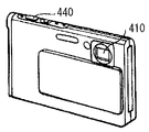
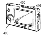
도 28a, 28b는, 상기 실시의 형태의 표시 장치가 적용되는 디지털 카메라의 외관을 도시한 것이다. 이 디지털 카메라는, 예를 들면, 플래시용의 발광부(410), 표시부(420), 메뉴 스위치(430) 및 셔터 버튼(440)을 갖고 있고, 그 표시부(420)는, 상기 각 실시의 형태에 관한 표시 장치에 의해 구성되어 있다.28A and 28B show the appearance of a digital camera to which the display device of the above embodiment is applied. This digital camera has, for example, a
(적용예 3)(Application Example 3)
도 29는, 상기 실시의 형태의 표시 장치(1)가 적용되는 노트형 퍼스널 컴퓨터의 외관을 도시한 것이다. 이 노트형 퍼스널 컴퓨터는, 예를 들면, 본체(510), 문자 등의 입력 조작을 위한 키보드(520) 및 화상을 표시하는 표시부(530)를 갖고 있고, 그 표시부(530)는, 상기 각 실시의 형태에 관한 표시 장치에 의해 구성되어 있다.Fig. 29 shows an appearance of a notebook personal computer to which the
(적용예 4)(Application Example 4)
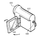
도 30은, 상기 실시의 형태의 표시 장치가 적용되는 비디오 카메라의 외관을 도시한 것이다. 이 비디오 카메라는, 예를 들면, 본체부(610), 이 본체부(610)의 전방 측면에 마련된 피사체 촬영용의 렌즈(620), 촬영시의 스타트/스톱 스위치(630) 및 표시부(640)를 갖고 있고, 그 표시부(640)는, 상기 각 실시의 형태에 관한 표시 장치에 의해 구성되어 있다.Fig. 30 shows an appearance of a video camera to which the display device of the above embodiment is applied. The video camera includes, for example, a
(적용예 5)(Application Example 5)
도 31a, 31b는, 상기 실시의 형태의 표시 장치가 적용되는 휴대 전화기의 외관을 도시한 것이다. 이 휴대 전화기는, 예를 들면, 상측 몸체(710)와 하측 몸체(720)를 연결부(힌지부)(730)로 연결한 것이고, 디스플레이(740), 서브 디스플레이(750), 픽처 라이트(760) 및 카메라(770)를 갖고 있다. 그 디스플레이(740) 또는 서브 디스플레이(750)는, 상기 각 실시의 형태에 관한 표시 장치에 의해 구성되어 있다.31A and 31B show the appearance of a mobile phone to which the display device of the above embodiment is applied. The
이상, 실시의 형태 및 변형예를 들어서 본 기술을 설명하였지만, 본 기술은 상기 실시의 형태 등으로 한정되는 것이 아니고, 여러가지 변형이 가능하다. 예를 들면, 상기 실시의 형태 등에서 설명한 각 층의 재료 및 두께, 또는 성막 방법 및 성막 조건 등은 한정되는 것이 아니고, 다른 재료 및 두께로 하여도 좋고, 또는 다른 성막 방법 및 성막 조건으로 하여도 좋다.Although the present invention has been described above with reference to the embodiments and the modified examples, the present technology is not limited to the above-described embodiments, and various modifications are possible. For example, the material and thickness of each layer described in the above embodiments and the like, or the film forming method and the film forming conditions are not limited, but may be different materials and thickness, or may be other film forming methods and film forming conditions .
또한, 상기 실시의 형태 등에서는, 제1 전극(21)을 양극, 제2 전극(23)을 음극으로 하는 경우에 관해 설명하였지만, 양극 및 음극을 역으로 하여, 제1 전극(21)을 음극, 제2 전극(23)을 양극으로 하여도 좋다. 또한, 본 기술을 보텀 이미션형의 표시 장치에 적용하여도 좋다.In the above-described embodiment, the case where the
더하여, 본 기술을 예를 들면 발광부(20)에 무기층을 갖는 무기 EL 표시 장치 등, 유기 EL 표시 장치 이외의 자발광형의 표시 장치에 적용하는 것도 가능하다.In addition, the present technique can be applied to a self-luminous display device other than the organic EL display device such as an inorganic EL display device having an inorganic layer in the
또한, 상기 실시의 형태 등에서는, 기록 트랜지스터(Tr1), 구동 트랜지스터(Tr2)의 구성을 구체적으로 설명하였지만, 이들의 배치는 반대라도 좋고, 또는 발광부(20)의 바로 아래에 다른 트랜지스터를 배치하도록 하여도 좋다. 더하여, 상기 실시의 형태 등에서는, 기록 트랜지스터(Tr1), 구동 트랜지스터(Tr2)의 소스·드레인 영역을 N형 웰 영역 내에, 수광부(30)를 P형 웰 영역 내에 각각 마련하도록 하였지만, 기록 트랜지스터(Tr1), 구동 트랜지스터(Tr2)의 소스·드레인 영역을 P형 웰 영역 내에, 수광부(30)를 N형 웰 영역 내에 마련하는 것도 가능하다.Although the configuration of the recording transistor Tr1 and the driving transistor Tr2 has been described in detail in the above embodiments and the like, the arrangement may be reversed, or another transistor may be disposed immediately below the
또한, 본 기술은 이하와 같은 구성도 취할 수 있다.The present technology can also take the following configuration.
(1) 표시 영역 내에, 발광부와, 상기 발광부로부터의 광을 수광하는 수광부를 갖는 표시 장치.(1) A display device having a light emitting portion and a light receiving portion for receiving light from the light emitting portion, in a display region.
(2) 또한, 상기 발광부를 구동하는 화소 구동 회로와, 상기 수광부의 수광량에 응하여 상기 화소 구동 회로에 보정 신호를 보내는 보정 회로를 갖는 상기 (1)에 기재된 표시 장치.(2) The display device according to (1), further comprising: a pixel driving circuit for driving the light emitting portion; and a correction circuit for sending a correction signal to the pixel driving circuit in response to the amount of light received by the light receiving portion.
(3) 상기 발광부 및 상기 수광부는, 기판의 표면에 마련되어 있는 상기 (1) 또는 (2)에 기재된 표시 장치.(3) The display device according to (1) or (2), wherein the light emitting portion and the light receiving portion are provided on the surface of the substrate.
(4) 상기 수광부는, 한 쌍의 전극의 사이에 광전 변환막을 갖고 있는 상기 (1) 내지 (3) 중 어느 하나에 기재된 표시 장치.(4) The display device according to any one of (1) to (3), wherein the light receiving portion has a photoelectric conversion film between a pair of electrodes.
(5) 상기 발광부는 기판의 표면에 마련되고, 상기 수광부는 상기 기판의 내부에 마련되어 있는 상기 (2)에 기재된 표시 장치.(5) The display device according to (2), wherein the light emitting portion is provided on a surface of a substrate, and the light receiving portion is provided inside the substrate.
(6) 상기 수광부는 포토 다이오드에 의해 구성되어 있는 상기 (5)에 기재된 표시 장치.(6) The display device according to (5), wherein the light receiving portion is constituted by a photodiode.
(7) 상기 기판은 실리콘층을 갖는 상기 (5) 또는 (6)에 기재된 표시 장치.(7) The display device according to (5) or (6), wherein the substrate has a silicon layer.
(8) 상기 실리콘층의 이면 부근에 상기 수광부가 마련되어 있는 상기 (7)에 기재된 표시 장치.(8) The display device according to (7), wherein the light receiving portion is provided near the back surface of the silicon layer.
(9) 상기 화소 구동 회로는 트랜지스터를 포함하고, 상기 트랜지스터가 상기 발광부와 평면시에서 겹쳐지는 위치에 마련되어 있는 상기 (5) 내지 (8) 중 어느 하나에 기재된 표시 장치.(9) The display device according to any one of (5) to (8), wherein the pixel driving circuit includes a transistor, and the transistor is provided at a position overlapping with the light emitting portion in plan view.
(10) 상기 트랜지스터 및 상기 수광부를 화소마다 가지며, 상기 트랜지스터와 상기 수광부는 서로 이웃하는 위치에 마련되어 있는 상기 (9)에 기재된 표시 장치.(10) The display device according to (9), wherein the transistor and the light-receiving portion are provided for each pixel, and the transistor and the light-receiving portion are provided at neighboring positions.
(11) 상기 트랜지스터와 상기 수광부와의 사이에 차폐부를 갖는 상기 (10)에 기재된 표시 장치.(11) The display device according to (10), wherein a shielding portion is provided between the transistor and the light receiving portion.
(12) 상기 차폐부는, 상기 기판의 홈에 매설된 절연막인 상기 (11)에 기재된 표시 장치.(12) The display device according to (11), wherein the shielding portion is an insulating film buried in the groove of the substrate.
(13) 상기 차폐부는, 상기 기판의 홈에 매설된 금속막인 상기 (11)에 기재된 표시 장치.(13) The display device according to (11), wherein the shielding portion is a metal film buried in the groove of the substrate.
(14) 상기 차폐부는, 상기 기판의 홈에 매설된 구리인 상기 (11)에 기재된 표시 장치.(14) The display device according to (11), wherein the shielding portion is copper buried in the groove of the substrate.
(15) 상기 수광부를 둘러싸도록 상기 차폐부가 마련되어 있는 상기 (11) 내지 (14) 중 어느 하나에 기재된 표시 장치.(15) The display device according to any one of (11) to (14), wherein the shielding portion is provided so as to surround the light-receiving portion.
(16) 상기 기판과 대향하는 반사부를 가지며, 상기 반사부에서 반사된 상기 발광부로부터의 광이 상기 수광부에 입사하는 상기 (5) 내지 (15) 중 어느 하나에 기재된 표시 장치.(16) The display device according to any one of (5) to (15), wherein the light from the light emitting portion having the reflecting portion facing the substrate and reflected by the reflecting portion is incident on the light receiving portion.
(17) 상기 반사부의 상기 기판과의 대향면은 포물곡면인 상기 (16)에 기재된 표시 장치.(17) The display device according to (16), wherein a surface of the reflective portion facing the substrate is a parabolic surface.
(18) 표시 장치를 구비하고, 상기 표시 장치는, 표시 영역 내에, 발광부와, 상기 발광부로부터의 광을 수광하는 수광부를 갖는 전자 기기.(18) An electronic apparatus having a display device, wherein the display device has a light emitting portion and a light receiving portion that receives light from the light emitting portion, in a display area.
(19) 화소 구동 회로에 의해 표시 영역 내의 발광부를 구동하고, 상기 발광부로부터의 광을 상기 표시 영역 내의 수광부에서 수광하고, 상기 수광부의 수광량에 응하여 보정 회로로부터 상기 화소 구동 회로에 보정 신호를 보내는 표시 장치의 구동 방법.(19) The light emitting element in the display area is driven by the pixel driving circuit, light from the light emitting element is received by the light receiving element in the display area, and a correction signal is sent from the correction circuit to the pixel driving circuit in response to the light receiving amount of the light receiving element A method of driving a display device.
(20) 표시 영역 내에, 발광부와 상기 발광부로부터의 광을 수광하는 수광부를 형성하는 표시 장치의 제조 방법.
(20) A light emitting portion and a light receiving portion for receiving light from the light emitting portion are formed in the display region.
1, 1a, 2, 2A, 3 : 표시 장치
10 : 화소
11 : 지지 부재
12 : 다층 배선층
13, 43 : 기판
13a : Si층
13b : 절연층
43a : 판형상 부재
43b : TFT층
13V : 관통 전극
13W1, 13W2, 13W3, 13W4, 13W5, 13W6, 13W7 : 도전성 플러그
Tr1, Tr2, Tr3 : 트랜지스터
TG1, TG2, TG3 : 게이트 전극
14 : 절연층
15 : 소자 분리층
16 : 보호층
17 : CF층
18, 18a : 반사부
19 : 대향 기판
20 : 발광부
21 : 제1 전극
22 : 유기층
23 : 제2 전극
30, 50 : 수광부
31, 32 : 차폐부1, 1a, 2, 2A, 3: display device
10: pixel
11: Support member
12: multilayer wiring layer
13, 43: substrate
13a: Si layer
13b: insulating layer
43a: Plate member
43b: TFT layer
13V: Through electrode
13W1, 13W2, 13W3, 13W4, 13W5, 13W6, 13W7: conductive plugs
Tr1, Tr2, Tr3: transistors
TG1, TG2, TG3: gate electrode
14: Insulating layer
15: Element isolation layer
16: Protective layer
17: CF layer
18, 18a:
19: opposing substrate
20:
21: first electrode
22: Organic layer
23: Second electrode
30, 50:
31, 32:
Claims (20)
표시 영역 내에 발광부와,
상기 발광부로부터의 광을 수광하는 수광부를 갖는 것을 특징으로 하는 표시 장치.In the display device,
A light emitting portion in the display region,
And a light receiving portion that receives light from the light emitting portion.
상기 발광부를 구동하는 화소 구동 회로와,
상기 수광부의 수광량에 응하여 상기 화소 구동 회로에 보정 신호를 보내는 보정 회로를 더 구비하는 것을 특징으로 하는 표시 장치.The method according to claim 1,
A pixel driving circuit for driving the light emitting portion,
And a correction circuit that sends a correction signal to the pixel driving circuit in response to the amount of light received by the light receiving portion.
상기 발광부 및 상기 수광부는, 기판의 표면에 마련되어 있는 것을 특징으로 하는 표시 장치.3. The method of claim 2,
Wherein the light emitting portion and the light receiving portion are provided on the surface of the substrate.
상기 수광부는, 한 쌍의 전극의 사이에 광전 변환막을 갖고 있는 것을 특징으로 하는 표시 장치.The method of claim 3,
Wherein the light receiving portion has a photoelectric conversion film between a pair of electrodes.
상기 발광부는 기판의 표면에 마련되고,
상기 수광부는 상기 기판의 내부에 마련되어 있는 것을 특징으로 하는 표시 장치.3. The method of claim 2,
The light emitting portion is provided on the surface of the substrate,
Wherein the light receiving portion is provided inside the substrate.
상기 수광부는 포토 다이오드에 의해 구성되어 있는 것을 특징으로 하는 표시 장치.6. The method of claim 5,
Wherein the light receiving portion is constituted by a photodiode.
상기 기판은 실리콘층을 갖는 것을 특징으로 하는 표시 장치.6. The method of claim 5,
Wherein the substrate has a silicon layer.
상기 실리콘층의 이면 부근에 상기 수광부가 마련되어 있는 것을 특징으로 하는 표시 장치.8. The method of claim 7,
And the light receiving portion is provided near the back surface of the silicon layer.
상기 화소 구동 회로는 트랜지스터를 포함하고, 상기 트랜지스터가 상기 발광부와 평면시에서 겹쳐지는 위치에 마련되어 있는 것을 특징으로 하는 표시 장치.6. The method of claim 5,
Wherein the pixel driving circuit includes a transistor, and the transistor is provided at a position overlapping with the light emitting portion in a plan view.
상기 트랜지스터 및 상기 수광부를 화소마다 가지며, 상기 트랜지스터와 상기 수광부는 서로 이웃하는 위치에 마련되어 있는 것을 특징으로 하는 표시 장치.10. The method of claim 9,
Wherein the transistor and the light receiving unit are provided for each pixel, and the transistor and the light receiving unit are provided at neighboring positions.
상기 트랜지스터와 상기 수광부와의 사이에 차폐부를 갖는 것을 특징으로 하는 표시 장치.11. The method of claim 10,
And a shielding portion between the transistor and the light receiving portion.
상기 차폐부는, 상기 기판의 홈에 매설된 절연막인 것을 특징으로 하는 표시 장치.12. The method of claim 11,
Wherein the shielding portion is an insulating film buried in the groove of the substrate.
상기 차폐부는, 상기 기판의 홈에 매설된 금속막인 것을 특징으로 하는 표시 장치.12. The method of claim 11,
Wherein the shielding portion is a metal film buried in the groove of the substrate.
상기 차폐부는, 상기 기판의 홈에 매설된 구리인 것을 특징으로 하는 표시 장치.12. The method of claim 11,
Wherein the shielding portion is copper buried in the groove of the substrate.
상기 수광부를 둘러싸도록 상기 차폐부가 마련되어 있는 것을 특징으로 하는 표시 장치.12. The method of claim 11,
And the shielding portion is provided so as to surround the light-receiving portion.
상기 기판과 대향하는 반사부를 가지며, 상기 반사부에서 반사된 상기 발광부로부터의 광이 상기 수광부에 입사하는 것을 특징으로 하는 표시 장치.6. The method of claim 5,
And the light from the light emitting portion reflected by the reflecting portion is incident on the light receiving portion.
상기 반사부의 상기 기판과의 대향면은 포물곡면인 것을 특징으로 하는 표시 장치.17. The method of claim 16,
Wherein a surface of the reflection portion facing the substrate is a parabolic surface.
표시 장치를 구비하고,
상기 표시 장치는, 표시 영역 내에 발광부와,
상기 발광부로부터의 광을 수광하는 수광부를 갖는 것을 특징으로 하는 전자 기기.In the electronic device,
A display device,
The display device has a light emitting portion,
And a light receiving portion for receiving light from the light emitting portion.
화소 구동 회로에 의해 표시 영역 내의 발광부를 구동하고,
상기 발광부로부터의 광을 상기 표시 영역 내의 수광부에서 수광하고,
상기 수광부의 수광량에 응하여 보정 회로로부터 상기 화소 구동 회로에 보정 신호를 보내는 것을 특징으로 하는 표시 장치의 구동 방법.A method of driving a display device,
The light emitting portion in the display region is driven by the pixel driving circuit,
The light from the light emitting portion is received by the light receiving portion in the display region,
And a correction signal is sent from the correction circuit to the pixel driving circuit in response to the amount of light received by the light receiving portion.
표시 영역 내에 발광부와,
상기 발광부로부터의 광을 수광하는 수광부를 형성하는 것을 특징으로 하는 표시 장치의 제조 방법.A method of manufacturing a display device,
A light emitting portion in the display region,
And a light receiving portion for receiving light from the light emitting portion is formed.
Applications Claiming Priority (4)
| Application Number | Priority Date | Filing Date | Title |
|---|---|---|---|
| JP2013037375 | 2013-02-27 | ||
| JPJP-P-2013-037375 | 2013-02-27 | ||
| JPJP-P-2013-159320 | 2013-07-31 | ||
| JP2013159320A JP2014194517A (en) | 2013-02-27 | 2013-07-31 | Display device, manufacturing method of the display device, drive method of the display device and electronic apparatus |
Publications (1)
| Publication Number | Publication Date |
|---|---|
| KR20140107123A true KR20140107123A (en) | 2014-09-04 |
Family
ID=51369649
Family Applications (1)
| Application Number | Title | Priority Date | Filing Date |
|---|---|---|---|
| KR1020140016591A KR20140107123A (en) | 2013-02-27 | 2014-02-13 | Display, method of manufacturing display, method of driving display, and electronic apparatus |
Country Status (4)
| Country | Link |
|---|---|
| US (1) | US20140240370A1 (en) |
| JP (1) | JP2014194517A (en) |
| KR (1) | KR20140107123A (en) |
| CN (1) | CN104009060A (en) |
Cited By (1)
| Publication number | Priority date | Publication date | Assignee | Title |
|---|---|---|---|---|
| KR20190098883A (en) * | 2018-02-14 | 2019-08-23 | 삼성디스플레이 주식회사 | Display device |
Families Citing this family (13)
| Publication number | Priority date | Publication date | Assignee | Title |
|---|---|---|---|---|
| KR102363429B1 (en) * | 2015-02-02 | 2022-02-17 | 삼성디스플레이 주식회사 | Organic light-emitting device |
| JP2017174936A (en) * | 2016-03-23 | 2017-09-28 | ソニー株式会社 | Solid state imaging device and electronic apparatus |
| US9961178B2 (en) | 2016-03-24 | 2018-05-01 | Motorola Mobility Llc | Embedded active matrix organic light emitting diode (AMOLED) fingerprint sensor |
| US20170289805A1 (en) * | 2016-03-30 | 2017-10-05 | Motorola Mobility Llc | Embedded active matrix organic light emitting diode (amoled) fingerprint sensor and self-compensating amoled |
| CN107393863A (en) * | 2017-05-22 | 2017-11-24 | 茆胜 | OLED minitype displayer IC pieces and preparation method thereof |
| CN107342375B (en) * | 2017-08-21 | 2019-05-31 | 深圳市华星光电半导体显示技术有限公司 | The production method and flexible display panels of flexible display panels |
| CN111095387B (en) * | 2017-09-22 | 2022-08-09 | 索尼公司 | Display element, display device, and electronic apparatus |
| CN111261106A (en) | 2018-11-30 | 2020-06-09 | 京东方科技集团股份有限公司 | Display panel and manufacturing method thereof, pixel luminescence compensation method and display device |
| CN109638047B (en) | 2018-12-13 | 2020-12-22 | 京东方科技集团股份有限公司 | Display panel, manufacturing method thereof and method for driving display panel |
| CN110265442B (en) * | 2019-06-14 | 2021-04-02 | 京东方科技集团股份有限公司 | Display substrate and display panel comprising same |
| CN111524943A (en) * | 2020-04-27 | 2020-08-11 | 武汉华星光电半导体显示技术有限公司 | Display panel and display device |
| WO2021225139A1 (en) * | 2020-05-08 | 2021-11-11 | ソニーグループ株式会社 | Display device and electronic device |
| CN113725379B (en) * | 2020-05-25 | 2022-12-09 | 京东方科技集团股份有限公司 | Display module and display device |
Family Cites Families (4)
| Publication number | Priority date | Publication date | Assignee | Title |
|---|---|---|---|---|
| JP2005159137A (en) * | 2003-11-27 | 2005-06-16 | Sharp Corp | Optical semiconductor device and electronic apparatus using it |
| GB0406107D0 (en) * | 2004-03-17 | 2004-04-21 | Koninkl Philips Electronics Nv | Electroluminescent display devices |
| KR100759681B1 (en) * | 2006-03-29 | 2007-09-17 | 삼성에스디아이 주식회사 | Organic light emitting diode |
| JP5310372B2 (en) * | 2009-08-12 | 2013-10-09 | ソニー株式会社 | Display device, luminance degradation correction method, and electronic device |
-
2013
- 2013-07-31 JP JP2013159320A patent/JP2014194517A/en active Pending
-
2014
- 2014-02-10 US US14/176,656 patent/US20140240370A1/en not_active Abandoned
- 2014-02-13 KR KR1020140016591A patent/KR20140107123A/en not_active Application Discontinuation
- 2014-02-20 CN CN201410058610.7A patent/CN104009060A/en active Pending
Cited By (1)
| Publication number | Priority date | Publication date | Assignee | Title |
|---|---|---|---|---|
| KR20190098883A (en) * | 2018-02-14 | 2019-08-23 | 삼성디스플레이 주식회사 | Display device |
Also Published As
| Publication number | Publication date |
|---|---|
| CN104009060A (en) | 2014-08-27 |
| US20140240370A1 (en) | 2014-08-28 |
| JP2014194517A (en) | 2014-10-09 |
Similar Documents
| Publication | Publication Date | Title |
|---|---|---|
| KR20140107123A (en) | Display, method of manufacturing display, method of driving display, and electronic apparatus | |
| CN109994522B (en) | Display device | |
| US9508285B2 (en) | Pixel array, metal mask, electro optical device and electric apparatus | |
| EP2207219B1 (en) | Organic light emitting diode display and method of manufacturing the same | |
| US8963170B2 (en) | Organic light emitting device and display unit including the same | |
| US8415675B2 (en) | Organic light emitting display device and method of fabricating the same | |
| KR100838082B1 (en) | Oled and method for fabricating the same | |
| US10332952B2 (en) | Display unit, method of manufacturing display unit, and electronic apparatus | |
| EP2139041B1 (en) | Luminescence display panel and method for fabricating the same | |
| KR102323630B1 (en) | Display unit, method of manufacturing the same, and method of manufacturing electronic apparatus | |
| EP2816627B1 (en) | Display device | |
| KR20140140484A (en) | Display unit, method of manufcturing display unit, and electronic apparatus | |
| KR20180004384A (en) | Organic light emitting display device and method of manufacturing the same | |
| KR20100090998A (en) | Organic light emitting diode display and method for manufacturing the same | |
| US10312471B2 (en) | Method of manufacturing display device, display device, and electronic device | |
| US20170033170A1 (en) | Organic light emitting diode display | |
| KR20150018030A (en) | Organic light emitting diode display | |
| KR102381901B1 (en) | Display device and manufacturing method thereof | |
| US20230345770A1 (en) | Display device and method of manufacturing the same | |
| KR20170049659A (en) | Organic light emitting diode display | |
| KR101511548B1 (en) | Light emitting diode display device and method for driving the same | |
| KR20160089011A (en) | Organic light emitting device | |
| JP2014049405A (en) | Display device and method for manufacturing the same, and electronic apparatus | |
| KR100975225B1 (en) | Organic Light Emitting Display Device and Method of Fabricating the Same | |
| KR100669774B1 (en) | Flat panel display and method for fabricating the same |
Legal Events
| Date | Code | Title | Description |
|---|---|---|---|
| N231 | Notification of change of applicant | ||
| WITN | Application deemed withdrawn, e.g. because no request for examination was filed or no examination fee was paid |