US8218537B1 - Dual signaling format switch fabric with multiplex capability - Google Patents
Dual signaling format switch fabric with multiplex capability Download PDFInfo
- Publication number
- US8218537B1 US8218537B1 US12/156,339 US15633908A US8218537B1 US 8218537 B1 US8218537 B1 US 8218537B1 US 15633908 A US15633908 A US 15633908A US 8218537 B1 US8218537 B1 US 8218537B1
- Authority
- US
- United States
- Prior art keywords
- channel
- switch
- serial
- logical
- data
- Prior art date
- Legal status (The legal status is an assumption and is not a legal conclusion. Google has not performed a legal analysis and makes no representation as to the accuracy of the status listed.)
- Active, expires
Links
- 239000004744 fabric Substances 0.000 title claims description 77
- 230000011664 signaling Effects 0.000 title claims description 13
- 230000009977 dual effect Effects 0.000 title description 6
- 238000013507 mapping Methods 0.000 claims abstract description 46
- 230000004044 response Effects 0.000 claims description 15
- 230000008878 coupling Effects 0.000 claims description 3
- 238000010168 coupling process Methods 0.000 claims description 3
- 238000005859 coupling reaction Methods 0.000 claims description 3
- 238000012163 sequencing technique Methods 0.000 claims 2
- 230000001351 cycling effect Effects 0.000 claims 1
- 238000013519 translation Methods 0.000 abstract description 4
- 238000000034 method Methods 0.000 description 21
- 239000004020 conductor Substances 0.000 description 17
- 240000008881 Oenanthe javanica Species 0.000 description 10
- 230000005540 biological transmission Effects 0.000 description 10
- 238000013461 design Methods 0.000 description 10
- 230000008569 process Effects 0.000 description 10
- 101150031442 sfc1 gene Proteins 0.000 description 10
- 238000010586 diagram Methods 0.000 description 9
- 230000002349 favourable effect Effects 0.000 description 8
- 101100020526 Pycnoporus cinnabarinus LCC3-1 gene Proteins 0.000 description 7
- 101100074140 Trametes versicolor LCC4 gene Proteins 0.000 description 7
- 230000008859 change Effects 0.000 description 7
- 101150075807 lcc1 gene Proteins 0.000 description 7
- 230000006870 function Effects 0.000 description 6
- 239000000872 buffer Substances 0.000 description 5
- 238000004891 communication Methods 0.000 description 5
- 108010028621 stem cell inhibitory factor Proteins 0.000 description 5
- 238000012546 transfer Methods 0.000 description 5
- 230000000694 effects Effects 0.000 description 4
- 101150069416 lcc3 gene Proteins 0.000 description 4
- 238000012986 modification Methods 0.000 description 4
- 230000004048 modification Effects 0.000 description 4
- 101000737578 Arabidopsis thaliana Bifunctional cystathionine gamma-lyase/cysteine synthase Proteins 0.000 description 3
- 101000952234 Homo sapiens Sphingolipid delta(4)-desaturase DES1 Proteins 0.000 description 3
- 101150014615 LCC2 gene Proteins 0.000 description 3
- 102100037416 Sphingolipid delta(4)-desaturase DES1 Human genes 0.000 description 3
- 230000008901 benefit Effects 0.000 description 3
- 230000015654 memory Effects 0.000 description 3
- 230000003068 static effect Effects 0.000 description 3
- 238000012360 testing method Methods 0.000 description 3
- 101100368149 Mus musculus Sync gene Proteins 0.000 description 2
- 238000013459 approach Methods 0.000 description 2
- 230000003111 delayed effect Effects 0.000 description 2
- 238000005457 optimization Methods 0.000 description 2
- 238000012545 processing Methods 0.000 description 2
- 230000008672 reprogramming Effects 0.000 description 2
- RYGMFSIKBFXOCR-UHFFFAOYSA-N Copper Chemical compound [Cu] RYGMFSIKBFXOCR-UHFFFAOYSA-N 0.000 description 1
- 101100365490 Drosophila melanogaster Jon99Ci gene Proteins 0.000 description 1
- 101100533228 Drosophila melanogaster Jon99Cii gene Proteins 0.000 description 1
- 101100533231 Drosophila melanogaster Jon99Ciii gene Proteins 0.000 description 1
- 101000918926 Homo sapiens Sphingolipid delta(4)-desaturase/C4-monooxygenase DES2 Proteins 0.000 description 1
- 240000007320 Pinus strobus Species 0.000 description 1
- 101150052146 SER2 gene Proteins 0.000 description 1
- 101100277598 Sorghum bicolor DES3 gene Proteins 0.000 description 1
- 102100029473 Sphingolipid delta(4)-desaturase/C4-monooxygenase DES2 Human genes 0.000 description 1
- 230000002457 bidirectional effect Effects 0.000 description 1
- 230000000903 blocking effect Effects 0.000 description 1
- 239000003990 capacitor Substances 0.000 description 1
- 239000000969 carrier Substances 0.000 description 1
- 230000015556 catabolic process Effects 0.000 description 1
- 230000000295 complement effect Effects 0.000 description 1
- 208000024858 congenital sideroblastic anemia-B-cell immunodeficiency-periodic fever-developmental delay syndrome Diseases 0.000 description 1
- 238000010276 construction Methods 0.000 description 1
- 229910052802 copper Inorganic materials 0.000 description 1
- 239000010949 copper Substances 0.000 description 1
- 125000004122 cyclic group Chemical group 0.000 description 1
- 230000007423 decrease Effects 0.000 description 1
- 238000006731 degradation reaction Methods 0.000 description 1
- 238000001514 detection method Methods 0.000 description 1
- 239000000835 fiber Substances 0.000 description 1
- 230000006872 improvement Effects 0.000 description 1
- 238000010348 incorporation Methods 0.000 description 1
- NUHSROFQTUXZQQ-UHFFFAOYSA-N isopentenyl diphosphate Chemical compound CC(=C)CCO[P@](O)(=O)OP(O)(O)=O NUHSROFQTUXZQQ-UHFFFAOYSA-N 0.000 description 1
- 230000008520 organization Effects 0.000 description 1
- 230000009467 reduction Effects 0.000 description 1
- 230000002787 reinforcement Effects 0.000 description 1
- 230000035945 sensitivity Effects 0.000 description 1
- 101150106567 ser1 gene Proteins 0.000 description 1
- 101150008449 ser3 gene Proteins 0.000 description 1
- 201000005956 sideroblastic anemia with B-cell immunodeficiency, periodic fevers, and developmental delay Diseases 0.000 description 1
- 238000001228 spectrum Methods 0.000 description 1
- 238000000564 temperature-controlled scanning calorimetry Methods 0.000 description 1
Images


Classifications
-
- H—ELECTRICITY
- H04—ELECTRIC COMMUNICATION TECHNIQUE
- H04L—TRANSMISSION OF DIGITAL INFORMATION, e.g. TELEGRAPHIC COMMUNICATION
- H04L49/00—Packet switching elements
- H04L49/10—Packet switching elements characterised by the switching fabric construction
- H04L49/101—Packet switching elements characterised by the switching fabric construction using crossbar or matrix
-
- H—ELECTRICITY
- H04—ELECTRIC COMMUNICATION TECHNIQUE
- H04L—TRANSMISSION OF DIGITAL INFORMATION, e.g. TELEGRAPHIC COMMUNICATION
- H04L49/00—Packet switching elements
-
- H—ELECTRICITY
- H04—ELECTRIC COMMUNICATION TECHNIQUE
- H04L—TRANSMISSION OF DIGITAL INFORMATION, e.g. TELEGRAPHIC COMMUNICATION
- H04L49/00—Packet switching elements
- H04L49/40—Constructional details, e.g. power supply, mechanical construction or backplane
Definitions
- the present disclosure relates generally to packet switch/router design and operation, and more particularly to techniques for reducing serial channel crosstalk across an electrical backplane.
- Packets switches/routers have external ports on which they receive and transmit packets. Most received packet traffic has a destination other than the switch/router itself.
- the packet/switch router determines, from a packet's headers, and possibly the port on which the packet is received, an appropriate output port or ports for each such packet. The packet is switched internally to the desired output port or ports that move the packet towards its destination.
- switch/routers have an internal switching architecture capable of sustaining an internal packet throughput at least roughly equal to the aggregate line rate of all the external ports on the switch/router (some architectures allow an “oversubscribed” configuration that assumes all external ports are operating on average at some fraction of their line rate).
- 10 Gbps (Billion bits/second) ports are now becoming common, and systems are in design for even higher line rate external ports.
- the internal switching architectures for medium-to-large switch/routers handling 10 Gbps and higher-speed external ports require internal throughputs measurable in Terabits/second (Tbps) to tens of Tbps.
- Tbps Terabits/second
- Such systems are modular, with the external ports hosted on multiple line cards that attach to one or more backplanes. Internal packet switching between line cards requires passing the packet data across a backplane.
- FIG. 1 shows one prior art data plane architecture for a high-speed switch/router 100 .
- the data plane architecture includes line cards LC 0 to LCn, switch fabric cards SF 0 to SFm, and a backplane 110 to which the line cards and switch fabric cards connect.
- Line cards can support different external signaling speeds and formats as needed for a particular application. All line card options are compatible, however, with the backplane and switch fabric cards.
- Line card LC 0 is representative of all line cards.
- Line card LC 0 contains physical interface devices PHY 0 . 0 , PHY 0 . 1 , PHY 0 . 2 , packet processor devices IPP 0 and EPP 0 , traffic manager devices ITM 0 and ETM 0 , and serializer/deserializer (SERDES) devices (grouped together as SDL 0 ), as well as other control plane devices (not shown) for managing the illustrated devices.
- Each physical interface device supports one or more external ports of a desired format and speed, to which external connections (e.g., copper cable or fiber optic cable) are made.
- the physical interface devices interpret the physical signaling for received packet data, and supply received packet data to an ingress packet processor device IPP 0 .
- Ingress packet processor IPP 0 provides any necessary updates to each packet, determines an appropriate egress port or ports for each packet, tags the packets with an internal header, and submits them to an ingress traffic manager ITM 0 for queuing. Ingress traffic manager ITM 0 queues each packet with others of similar priority that are destined for the same egress line card, and notifies a central scheduler (not shown) as to which queues have data waiting. When instructed by the scheduler, packets bound for a particular egress line card are dequeued and presented to SERDES SDL 0 for transmission across the backplane.
- line card LC 0 SERDES SDL 0 receives packet data for packets that an ingress processor has determined have an egress port served by line card LC 0 .
- SERDES SDL 0 deserializes the packet data and supplies the data to an egress traffic manager ETM 0 for queuing.
- ETM 0 supplies the packets to an egress packet processor EPP 0 in a manner that attempts to treat packets of similar priority fairly.
- Egress packet processor EPP 0 performs any necessary packet header manipulation, removes the internal tag headers, and supplies the packets to the appropriate physical interface device for transmission on an external port.
- Backplane 110 connects the line cards and switch fabric cards to the system.
- Backplane 110 contains male connectors, e.g., CML 0 , aligned to connect with companion line card female connectors, e.g., connector CFL 0 on line card LC 0 .
- Backplane 110 also contains male connectors, e.g., CMS 0 , aligned to connect with companion switch fabric card female connectors, e.g., connector CFS 0 on switch fabric card SF 0 .
- backplane 110 contains differential trace pairs connecting designated pins of each line card male connector to each switch fabric male connector. For instance, at each line card slot, one defined connector pin pair supports transmission across a differential trace pair to switch fabric card SF 0 , and another defined connector pin pair supports reception across a differential trace pair from switch fabric card SF 0 . Other defined connector pin pairs at each line card slot support transmission and reception to other switch fabric cards, and/or additional channels to switch fabric card SF 0 . Likewise, at each switch fabric card slot, one defined connector pin pair supports transmission across a differential trace pair to line card LC 0 , and another defined connector pin pair supports reception across a differential trace pair from line card LC 0 . Other defined connector pin pairs at each switch fabric card slot support transmission and reception to/from other line cards, and/or additional channels to line card LC 0 .
- Switch fabric card SF 0 is representative of all switch fabric cards.
- Switch fabric card SF 0 contains a crossbar switch CS 0 and SERDES devices (grouped together as SDS 0 ), as well as other control plane devices (not shown) for managing the illustrated devices.
- the SERDES devices SDS 0 function like the line card SERDES devices, such that each device communicates across a backplane differential trace pair with a paired device.
- Each SERDES submits parallel data to the crossbar switch CS 0 , and receives parallel data from the crossbar switch (this is generally true, although some channels could be idle, depending on the crossbar configuration).
- a central scheduler (not shown) supplies the crossbar switch CS 0 with a configuration schedule that describes the crossbar configurations desired to effectuate the transfer of packets from their respective ingress line cards to their respective egress line cards.
- the configuration schedule changes the crossbar configuration once per epoch, where each epoch allows each scheduled line card the opportunity to transmit (as typically configured) tens of thousands of octets of packet data to a target line card.
- a line card selects packets from one or more queues corresponding to the scheduled destination, divides the packet data for parallel transmission to all of the switch fabric cards, and sends the packet data to the switch fabric cards at the appropriate epoch.
- the crossbar switches turn the packet data simultaneously to the appropriate egress channels to reach the scheduled egress line card—which receives and reassembles the packet data. Many such transfers can occur simultaneously during the same epoch, with the scheduler scheduling as many non-conflicting transfers as possible each epoch.
- a hybrid signaling scheme is used to send data across the backplane.
- Each transmitting SERDES constructs a backplane epoch frame 200 , illustrated in FIG. 2 .
- the packet headers and data supplied by the ITM to the SERDES are scrambled prior to transmission.
- the remainder of epoch frame 200 is transmitted using 8b/10b block coding, as follows.
- Each frame begins and ends with a string of 8b/10b alignment characters (see portions of epoch frame 200 labeled “SYNC”), which each SERDES transmits when it has no other data to send.
- SYNC portions of epoch frame 200 labeled “SYNC”
- SOE start of epoch
- the start character is followed by scrambled packet headers/data, a cyclic redundancy check trailer CRC in 8b/10b format, and a back channel trailer BCH in 8b/10b format.
- the SERDES resumes transmitting alignment characters until the next SOE is received.
- FIG. 3 shows a block diagram 300 for a SERDES transmit/receive pair as used in switch/router 100 .
- Parallel data DATA IN is scrambled by a scrambler upon the command of a control block.
- the control block also produces the 8b/10b control and header/trailer characters, and operates a multiplexer that merges the 8b/10b characters with the scrambler output SCR for submission to a differential transmitter Tx.
- the control block resets the scrambler with a seed value at the beginning of each epoch.
- a differential receiver Rx senses data and recovers timing for a received differential signal.
- a SYNC block detects the 8b/10b alignment characters in the data stream and aligns the data appropriately on 8b/10b word boundaries.
- An inbound control block receives the 8b/10 control and header/trailer characters through a demultiplexer, and directs the scrambled data to a descrambler. The descrambler is reset from a seed register each epoch, allowing it to create descrambled DATA OUT.
- the inbound control block may receive back channel data BCH that comprises transmit tap coefficient instructions for Tx, which the inbound control block passes to the outbound control block.
- the inbound control block may also receive back channel data BCH that allows it to adjust the decision feedback equalization (DFE) taps in Rx.
- DFE decision feedback equalization
- FIG. 1 shows, in block diagram form, various data plane components of a prior art modular switch/router
- FIG. 2 shows a hybrid scrambled epoch frame format useful with the modular switch/router of FIG. 1 ;
- FIG. 3 contains a block diagram for a SERDES receive/transmit pair useful with the modular switch/router of FIG. 1 and the epoch frame format of FIG. 2 ;
- FIG. 4 depicts, in block diagram form, various data plane components of a modular switch/router according to an embodiment
- FIG. 5 contains a block diagram for a serial/parallel crossbar switch according to an embodiment
- FIG. 6 illustrates several epoch data formats possible with the crossbar switch of FIG. 5 ;
- FIG. 7 shows an arrangement of serializer/deserializers, adapters, and input/output blocks for one embodiment of the FIG. 5 crossbar switch
- FIG. 8 depicts further details of the arrangement of one of the input/output blocks for one embodiment of the FIG. 5 crossbar switch
- FIG. 9 illustrates a block diagram for one embodiment of a receiver block in the input/output block embodiment of FIG. 8 ;
- FIG. 10 illustrates a block diagram for one embodiment of a transmit block in the input/output block embodiment of FIG. 8 ;
- FIG. 11 shows a block diagram for the crossbar core configuration in one embodiment of the FIG. 6 crossbar switch
- FIG. 12 details one embodiment for a logical-to-physical port mapper in one embodiment of the FIG. 6 crossbar switch
- FIG. 13 depicts, in plane view, an exemplary backplane layout for which the described embodiments are useful
- FIG. 14 shows, from a board edge view, various components of a serial channel connecting a line card crossbar switch circuit to a switch fabric crossbar switch circuit according to an embodiment
- FIG. 15 contains a flowchart for a decision process, according to an embodiment, for selecting serializer-deserializer pairings in a backplane layout
- FIGS. 16 , 17 , and 18 show, for a reduced complexity example, two crossbar serializer-deserializer pairings and three logical channel pairings;
- FIGS. 19 and 20 show, for the crossbar serializer-deserializer pairing of FIG. 16 , logical channel pairings that bypass a bad backplane channel;
- FIG. 21 shows a two-way path including components of two connected serial crossbar switches and two intermediate backplane connectors
- FIG. 22 contains a flowchart for a dynamic decision process for changing serdes characteristics and logical channel characteristics at run time to cope with crosstalk.
- line card traffic managers and backplane schedulers operate on a set of logical backplane channels.
- a line card ingress traffic manager submits packets to a given ingress logical channel set, and a line card egress traffic manager receives packets from a given egress logical channel set, both corresponding to the line card slot.
- the physical arrangement and signaling parameters for the physical channels corresponding to the logical channel set may differ both statically and dynamically.
- the management of the physical channels is ideally transparent to the traffic managers and schedulers (although either can, in some embodiments, participate in the implementation of dynamic logical-to-physical channel solutions).
- the backplane physical channel routing constraints previously imposed by modularity are relaxed to allow better physical channel routing solutions during backplane design.
- channel performance can be improved dynamically by a variety of techniques that influence the crosstalk relationship between a victim backplane physical channel and its neighboring aggressor backplane physical channels.
- FIG. 4 shows a data plane layout for one packet switch embodiment 400 .
- line cards LC 0 to LCn communicate with switch fabric card SF 0 to SFm.
- each backplane connection connects a crossbar switch on a line card to a crossbar switch on a switch fabric card.
- an ingress packet processor IPP 0 serves ingress packets
- an egress packet processor EPP 0 serves egress packets.
- the ingress packet processor IPP 0 has a group of serializers that connect to corresponding deserializers on crossbar switch LCX 0 .
- the egress packet processor EPP 0 has a group of deserializers that connect to corresponding serializers on crossbar switch LCX 0 .
- IPP 0 and EPP 0 are the same type of device, programmed appropriately for ingress and egress packet flow, respectively. Since each has a group of serializers and a group of deserializers, the unused serializers on EPP 0 are coupled to the unused deserializers on IPP 0 , allowing EPP 0 to pass egress lookup requests, mirrored traffic, and control packets to IPP 0 .
- IPP 0 in turn passes egress lookup responses to EPP 0 using SER-DES pairs on the PHY side of the processors. This usage allows all lookups to be performed on IPP 0 , allowing EPP 0 to function without separately supporting a second lookup memory. These serializer/deserializer connections are also useful in a loopback test mode.
- Crossbar switch LCX 0 distributes packet data from IPP 0 to the switch fabric cards according to a crossbar configuration, and also distributes packet data from the switch fabric cards to EPP 0 according to the crossbar configuration.
- the crossbar configuration for LCX 0 is set at boot time.
- the crossbar configuration is changed on an epoch basis, depending on the target for ingress packets and/or the source for egress packets.
- Each line card crossbar switch distributes and collects serial channel data from all of the switch fabric crossbar switches, and vice versa.
- a common ASIC is used both for the line card crossbar switches and the switch fabric crossbar switches. The design of this ASIC will now be described for an exemplary crossbar switch SFXi.
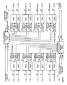
- FIG. 5 contains a high-level block diagram for crossbar switch SFXi, in an embodiment having 32 serial channel inputs (0 . . . 31) and 32 serial channel outputs (0 . . . 31).
- Eight quad serdes blocks, QS 0 to QS 7 each handle serialization and deserialization, respectively, for four of the serial channel inputs and four of the serial channel outputs.
- Each quad serdes QSi communicates respectively with a quad serdes adapter, QSAi.
- the quad serdes adapter transforms each deserialized serial data lane between a 10-bit wide format used by the quad serdes and a 20-bit wide format, at half the clock rate, used by the crossbar input and output blocks.
- the quad serdes adapter also transforms backchannel messaging between a Management Data Input/Output (MDIO) two-wire format used to access registers in the quad serdes and a sixteen-bit data+address/control format used to pass backchannel information within SFXi.
- MDIO Management Data Input/Output
- Each quad serdes adapter QSAi transmits its ingress channels to a corresponding quad input block QIBi, and receives its egress channels from a corresponding quad output block QOBi.
- QIBi removes and interprets serial channel control characters/channel information and buffers the packet data for submission to the crossbar XB.
- QOBi receives packet data from crossbar XB, taking each channel and adding control characters/channel information to create proper frames for transmission out the quad serdes adapter.
- Crossbar XB has the capability to place each of 65 20-bit-wide inputs (8 each for each quad input block, plus an “idle character” input), on any/all of 64 20-bit-wide outputs (8 each for each quad output block).
- the crossbar is programmed by a logical-to-physical mapping block LPMAP, which loads a switch configuration SWC to crossbar XB and then activates the switch configuration with the delayed start-of-epoch signal DSOE.
- Crossbar configuration is loaded to SFXi, including LPMAP, through a scheduling interface SIF supporting a scheduling bus.
- the scheduling bus includes address lines SIFA, bidirectional data lines SIFD, and control lines SIFC.
- a separate, two-wire MDIO interface is also provided for management loads of LPMAP settings.
- Both SIF and MDIO also support reads and writes from a set of configuration registers CFREG, which store configuration for SFXi.
- Each quad input block/output block QIBi/QOBi supports the routing of backchannel data between the channels of its attached quad serdes QSi.
- each quad input block/output block also communicates over a backchannel share bus with a backchannel arbiter BCH_ARB.
- the optional backchannel arbiter allows backchannel information received on any deserializer to be passed to any serializer, and backchannel information requested by any deserializer to be transmitted out any serializer.
- each quad serdes deserializer can be configured to detect either a non-return-to-zero (NRZ) two-level input symbol stream, or a four-level pulse amplitude modulation (PAM4) input symbol stream.
- NRZ non-return-to-zero
- PAM4 pulse amplitude modulation
- each quad serdes serializer can be configured to generate either a NRZ or PAM4 output symbol stream. When configured for NRZ operation, only the “A” data stream is active.
- each 2-bit PAM4 signal When configured for PAM4 operation, each 2-bit PAM4 signal consists of one “A” data stream bit and one “B” data stream bit. These data streams pass separately through SFXi, and thus two data streams received by one deserializer can be switched in parallel to the same serializer, or alternately can be split and sent to separate serializers, either as “A” or “B” channels.
- Each data stream can also take one of several different formats.
- One format uses 8b/10b coding for both control and data.
- Another format uses 8b/10b coding for control, and scrambling for data.
- a preferred scrambler is an X 29 +X 19 +1 scrambler, which approximates the signal spectrum of an 8b/10b data stream and thus the 8b/10b control characters used in each epoch frame.
- SFXi can perform CRC checks on incoming data streams, generate CRC fields on outgoing data streams, detect backchannel data on incoming data streams (“A” data streams only), and place backchannel data on outgoing data streams (“A” data streams only).
- FIG. 6 illustrates four of the possible serial channel data modes.
- the first is an NRZ mode at one-half line rate. In this mode, only A channel data is sent to a serializer or detected by a deserializer, and the B channel is unused.
- the A channel consists of an 8b/10b SYNC preamble, an 8b/10b start character S, scrambled headers/data of a defined data length, an optional 8b/10b CRC record, an optional 8b/10b BCH record, and an 8b/10b SYNC postamble.
- each line card crossbar serial channel to an IPP or EPP uses this first format.
- the second serial channel data mode shown in FIG. 6 is a half-scheduled PAM4 mode. In this mode, PAM4 signaling is used but only one of the PAM4 channels is scheduled to transmit data.
- the A-channel follows the same format as used above for NRZ mode.
- the B channel consists of an 8b/10b SYNC preamble, a continuation of 8b/10b SYNC characters instead of a start character and scrambled headers/data of the defined length, an optional 8b/10b CRC record, and an 8b/10b SYNC postamble.
- the third serial channel data mode shown in FIG. 6 is a full-scheduled PAM4 mode transmitting data using 8b/10b coding (and thus only 80% efficient).
- the A channel consists of an 8b/10b SYNC preamble, A-channel data coded as 8b/10b data characters of the defined length, an optional 8b/10b CRC record, an optional 8b/10b BCH record, and an 8b/10b SYNC postamble.
- the B channel is similar, but constructed with B-channel data, and without the option of a BCH record.
- the fourth serial channel data mode shown in FIG. 6 is a full-scheduled PAM4 mode transmitting data using scrambling.
- the A channel consists of an 8b/10b SYNC preamble, an 8b/10b start character S, scrambled headers/data of a defined data length, an optional 8b/10b CRC record, an optional 8b/10b BCH record, and an 8b/10b SYNC postamble.
- the B channel is similar, but constructed with B-channel data, and without the option of a BCH record.
- FIG. 5 SFXi embodiment The various functional blocks for the FIG. 5 SFXi embodiment are shown in more detail in FIGS. 7-12 , and will now be described with reference to the data format of FIG. 6 as necessary.
- the quad serdes comprises four serializers SER 0 , SER 1 , SER 2 , and SER 3 , four deserializers DES 0 , DES 1 , DES 2 , and DES 3 , and an MDIO interface MDIO IF.
- the quad serdes adapter comprises four subchannel adapters QSA 0 . 0 , QSA 0 . 1 , QSA 0 . 2 , and QSA 0 . 3 , and a serdes control interface SCIF.
- An ingress differential serial pair IiDS delivers either an NRZ or PAM4 signal to each deserializer DESi.
- the deserializer detects the clock timing of the received signal from the signal, at the line rate clock frequency LR clock. This frequency is divided by 10 and used as signal IiCK to clock received data buses to a quad serdes subchannel adapter QSA 0 . 1 .
- DESi buffers the received bits and transmits them in parallel 10-bit groups Ii.A to QSA 0 . 1 over a 10-bit parallel bus.
- DESi buffers the received bits and transmits them in two parallel 10-bit groups Ii.A and Ii.B to QSA 0 . 1 , with bits distributed alternately to the two groups.
- Each quad serdes subchannel adapter QSA 0 . 1 buffers Ii.A and Ii.B into an SFXi clock domain that is approximately LR/20, but may differ slightly from the clock rate of each received channel. As the clock rate is halved, the bus width on each bus is doubled to 20 bits, with two consecutive groups of 10 bits transmitted to QIB 0 on each clock cycle.
- QOB 0 transmits 20 bits on Ei.A and 20 bits on Ei.B in parallel at a LR/20 clock rate to QSA 0 . 1 .
- QSA 0 . 1 buffers the bits on each 20-bit lane, and transmits the bits over 10-bit lanes to SERi at twice the clock rate (LR/10), referenced from the SFXi clock.
- a clock EiCK is also supplied to SERi at LR/10 to facilitate reception of the data (this clock may alternately be driven from SERi to QSA 0 . 1 ).
- SERi is set to NRZ format
- Ei.B is ignored and
- Ei.A is NRZ-coded at an LR clock rate onto an egress differential serial pair EiDS.
- PAM4 format at each LR clock rate cycle one bit from E 0 .A and a corresponding bit from E 0 .B are coded as a PAM4 symbol onto the egress differential serial pair EiDS.
- the quad serdes adapter also interfaces with the register group MDIO IF across an MDIO bus.
- Register group MDIO IF contains registers accessed by each serializer SERi and each deserializer DESi to control serdes operation.
- Each deserializer also sends messages to the serializer on the other end of its serial channel by writing the messages to designated registers that are polled by SCIF.
- SCIF reads a new message from one of these designated registers, it relays the message to QOB 0 over a backchannel transmit share bus TXC (control/valid bits), TXD (data), indicating the message and the DESi that created the message.
- FIG. 8 shows the internal organization of a quad input block QIB 0 /quad output block QOB 0 .
- Each subchannel receiver RXi.A receives a 20-bit-wide data stream Ii.A from a corresponding quad subchannel adapter QSA 0 . 1 (see FIG. 7 ).
- RXi.A processes data stream Ii.A, as will be described in conjunction with FIG. 10 , to produce a 20-bit-wide data stream DINi.A and a corresponding set of flags DFLi.A to the crossbar.
- RXi.A may detect and extract a backchannel record from a received epoch frame, and transmit the backchannel record to the receive backchannel merger RX 0 .
- Each subchannel receiver RXi.B operates in similar fashion to process a 20-bit-wide data stream Ii.B from QSA 0 . 1 , producing a 20-bit-wide data stream DINi.B and a corresponding set of flags DFLi.B to the crossbar. As backchannel records are not carried on the B channel, the B subchannel receivers do not connect to the receive backchannel merger RX 0 . 3 .
- RX backchannel merger RX 0 . 3 arbitrates between it inputs RXDi, RXCi as needed, accepting backchannel records from the four subchannel receivers. These backchannel records are forwarded by RX 0 . 3 to the appropriate serdes adapter.
- backchannel records are only supported when the deserializer receiving the record and the serializer target of the record exist on the same quad serdes. In this case, RX 0 . 3 forwards all backchannel records to its directly attached quad serdes adapter over the receive backchannel bus RXD (16-bits-wide, data), RXC (control).
- the serializer target of a backchannel record is allowed to exist on any quad serdes in the device. In this case, receive backchannel merger RX 0 .
- a master backchannel arbiter BCH_ARB ( FIG. 5 ) can connect separately to each backchannel merger and arbitrate traffic to and from each.
- Each subchannel transmitter TXi.A receives a 20-bit-wide data stream DOUi.A and a corresponding set of flags DFLi.A from the crossbar.
- Subchannel transmitter TXi.A processes data stream DOUi.A, as will be described in conjunction with FIG. 10 , to produce a 20-bit-wide data stream Ei.A to a corresponding quad subchannel adapter QSA 0 . 1 (see FIG. 7 ).
- TXi.A may accept backchannel record data over a backchannel transmit bus TXDi (16-bits-wide, data), TXCi (control) from transmit backchannel splitter TX 0 .
- Each subchannel transmitter TXi.B operates in similar fashion to process a 20-bit-wide data stream DOUi.B and a corresponding set of flags DFLi.B received from the crossbar, producing a 20-bit-wide data stream Ei.B to QSA 0 . 1 .
- the B subchannel transmitters do not connect to the transmit backchannel splitter TX 0 . 3 .
- Transmit backchannel splitter TX 0 . 3 distributes backchannel record data over its output buses TXDi, TXCi as needed, sending backchannel record data as requested to the four subchannel transmitters.
- the backchannel record data is received by TX 0 . 3 from an appropriate serdes adapter.
- backchannel records are only supported when the deserializer generating the record data and the serializer generating the backchannel record exist on the same quad serdes.
- TX 0 . 3 receives all backchannel records from its directly attached quad serdes adapter over the transmit backchannel bus TXD (16-bits-wide, data), TXC (control).
- the serializer target of backchannel record data is allowed to exist on any quad serdes in the device.
- transmit backchannel merger TX 0 . 3 determines, based on the deserializer that requested a backchannel record, whether the target serializer is on the locally attached serdes adapter or not. If not, the backchannel record is forwarded out a transmit backchannel master bus TXMD (16-bits-wide, data), TXMC (control).
- TXMD (16-bits-wide, data)
- TXMC control
- Other backchannel splitter blocks can connect directly to this bus and monitor all traffic directly for traffic of interest.
- a master backchannel arbiter BCH_ARB FIG. 5 ) can connect separately to each backchannel splitter and arbitrate traffic to and from each.
- FIG. 9 shows the internal logic details of a representative subchannel receiver RX 0 .A.
- Subchannel receiver RX 0 .A receives a 20-bit-wide raw data signal I 0 .A from a subchannel adapter, configuration inputs for K,R,C,B character configuration, epoch mode selection MODE_SEL, a CRC function enable CRC_EN, a DATA_EXTENT value, and a delayed start-of-epoch timing signal DELAYED_SOE.
- Subchannel receiver RX 0 .A transmits crossbar-formatted data DIN 0 .A and corresponding flags (including a CRC error flag CRC_ERR and a detected frame format error flag FRAME_ERRS) to the crossbar, and receives backchannel data over a receive backchannel bus RXD 0 , RXC 0 .
- the 20-bit-wide raw data signal I 0 .A is input to a comma detection/20-bit alignment block CDA.
- CDA searches for the seven-bit comma pattern inside the KR 8b/10b pairs of symbols, either K+, R+ or K ⁇ , R ⁇ . When the comma pattern is found, CDA performs a circular shift on the data lanes such that K,R character sets are aligned to start on lane 0 of an output 20-bit bus AL_CHAR.
- CDA also asserts a signal COMMA_ALIGN to a receiver state controller RXSC when it believes it has achieved lock with the proper data alignment.
- State controller RXSC controls the operation of the remaining logical units of subchannel receiver RX 0 .A, which include: a dual 8b/10b decoder DD, a dual K,R,C,B character matcher CM, a CRC-24 checker CC, a receive data multiplexer RMUX, a receive data FIFO, a CRC-8 checker CRC8, and a backchannel record interface RXIF.
- RXSC bypasses all data sensing functions by setting a signal MUX_SEL such that RMUX passes the aligned data AL_CHAR from an input D 0 of RMUX directly through to the receive data FIFO.
- State controller RXSC also controls when data is pushed through the receive FIFO by asserting a FIFO_LD signal in response to the DELAYED_SOE input.
- the FIFO is provided to allow deskew of the data lanes, and in an alternate implementation could be provided prior to the input to RX 0 .A.
- the character stream on AL_CHAR is decoded by the 8b/10b decoder DD, producing dual 8-bit decoded characters DEC_CHAR and a two-bit control character code CTL_CHAR, indicating whether each of the dual characters is a control or a data character.
- the decoder When the decoder encounters an illegal character, it asserts a signal DEC_ERR to state controller RXSC.
- DEC_CHAR, CTL_CHAR, and a two-bit stuffing value “00” are supplied to an alternate input D 1 of RMUX, allowing RXSC to pass a decoded bitstream to the crossbar by selecting RMUX input D 1 .
- Character matcher CM compares each indicated decoded control character against the configurable character types K, R, C, and B. CM indicates to state controller RXSC whenever a K, R, C, or B control character is located in the data stream.
- CRC-24 checker CC tests the data portion of each epoch for transmission errors.
- state controller RXSC asserts a VALIDATE input to CRC-24 checker CC to instruct the checker to begin accumulating a CRC value based on the aligned character data stream AL_CHAR.
- CRC-24 checker CC then counts DATA_EXTENT data words while accumulating a CRC-24 value.
- a “C” control character following DATA_EXTENT scrambled or unscrambled values indicates the presence of a CRC-24 checksum record in the received data stream.
- state controller RXSC asserts a signal BKCH_LD to the receive backchannel interface RXIF and CRC checker CRC8.
- BKCH_LD causes RXIF and CRC8 to load four decoded characters from the DEC_CHAR bus, including the backchannel record data and backchannel CRC value.
- CRC8 calculates a CRC-8 value from the received 16-bit backchannel record data and compares the calculated and received CRC-8 values.
- CRC8 asserts BKCH_ERR to RXSC when the CRC check fails, thus preventing corrupted backchannel data from affecting the transmitters. Assuming that the backchannel message was received correctly, RXIF then negotiates with RX 0 . 3 ( FIG. 8 ) to effect the transfer of the backchannel record to the appropriate target.
- the B-channel subchannel receivers are similar to the depicted A-channel subchannel receiver, without the backchannel receive/transmit functionality.
- FIG. 10 shows the internal logic details of a representative subchannel transmitter TX 0 .A.
- Subchannel transmitter TX 0 .A receives a 20-bit-wide data signal DOU 0 .A from the crossbar, configuration inputs for K,R,C,B character configuration, an epoch mode selection configuration MODE_SEL, a DELAYED_SOE signal, a DATA_EXTENT value, and optional backchannel record data over a transmit backchannel bus TXD 0 , TXC 0 .
- Subchannel transmitter TX 0 .A transmits a 20-bit-wide aligned data stream E 0 .A, which includes continuously concatenated frame data, to a serdes adapter.
- a transmit state controller TXSC controls the construction of the A-channel epoch frame data according to the mode selected by MODE_SEL.
- State controller TXSC selects, using a signal SRC_SEL, one of two inputs, D 0 and D 1 , to a 20-bit ⁇ 2 multiplexer TMUX to be output on E 0 .A.
- transmit state controller TCSC determines based on mode and position in the data stream whether to transmit on E 0 .A, at each transmit clock period, either 20-bit data received from the crossbar (TMUX input D 0 ), or 20-bit data constructed by the components of TX 0 .A (TMUX input D 0 .
- TX 0 .A merely copies crossbar data onto output E 0 .A.
- some or all of the crossbar data is transformed within TX 0 .A, and in still other modes, some of the crossbar data is ignored/replaced with sync sequences and/or CRC records and/or backchannel records created by TX 0 .A.
- Subchannel transmitter TX 0 .A has the ability to encode 8b/10b data, using a dual 8b/10b encoder DE, as required for any particular mode.
- Data to be encoded is supplied as two nine-bit inputs to encoder DE, each input including eight bits of data or control word, and one bit indicating whether the input is data or control.
- Encoder DE performs two 8b/10b encodings in parallel, producing two 10-bit coded characters that are supplied in parallel to TMUX input D 1 .
- the input to encoder DE is the output of an 18-bit ⁇ 4 source multiplexer SMUX.
- State controller TXSC when creating output through decoder SMUX, uses control lines 8B10B_SEL to select one of four inputs D 0 , D 1 , D 2 , D 3 to pass to encoder DE.
- the four inputs include: at D 0 , 18 bits of DOU 0 .A; at D 1 , the control sequence KR, as supplied from configuration values K_CHAR, R_CHAR; at D 2 , a backchannel record; and at D 3 , a CRC record.
- state controller TXSC When the transmitter mode is one that creates a CRC record, state controller TXSC generates a START signal to a CRC-24 generator CG.
- CRC-24 generator CG searches for and detects a start character in the output E 0 .A, where the start character is any control character that is not one of the programmed K, R, C, and B characters. This causes generator CG to begin calculating a CRC value for the data passing across E 0 .A and counting the characters passing across E 0 .A. After the set number of data characters in an epoch DATA_EXTENT have passed through on E 0 .A, generator CG outputs its calculated 24-bit CRC.
- State controller TXSC then creates the CRC record in the data using an 18-bit ⁇ 2 CRC multiplexer CMUX.
- CMUX an input D 0 of CMUX is selected, causing CMUX to output a C control character (the configuration value C_CHAR) and the first 8 bits of the 24-bit CRC.
- C_CHAR the configuration value
- C_CHAR the configuration value
- C_CHAR the configuration value
- C_CHAR the configuration value
- the backchannel record data is loaded to a backchannel transmit interface TXIF over a backchannel transmit bus TXD 0 , TXC 0 .
- TXIF asserts a backchannel data ready signal BK_CTL to state controller TXSC.
- state controller TXSC creates a backchannel record using an 18-bit ⁇ 2 backchannel multiplexer BMUX.
- state controller TXSC uses a select signal BK_SEL to select an input D 0 of BMUX to be passed through SMUX to encoder DE.
- Input D 0 of BMUX is programmed with a B control character (the configuration value B_CHAR) and a CRC-8 value, output from a CRC-8 generator CRC8 that calculates the CRC from the backchannel message.
- B_CHAR the configuration value
- CRC-8 generator CRC8 that calculates the CRC from the backchannel message.
- the backchannel record data stored in TXIF is supplied to input D 1 of BMUX and selected to be passed through SMUX to encoder DE.
- the B-channel subchannel transmitters are similar to the depicted A-channel subchannel transmitter, without the backchannel receive/transmit functionality.
- FIG. 11 depicts the logical structure for one embodiment of the crossbar XB from FIG. 5 .
- Crossbar XB has 64 20-bit-wide data inputs, DIN 0 .A to DIN 31 .A and DIN 0 .B to DIN 31 .B.
- crossbar XB has 64 20-bit-wide data outputs, DOU 0 .A to DOU 31 .A and DOU 0 .B to DOU 31 .B.
- Crossbar XB can be programmed to switch any of the 64 inputs to any of the 64 outputs, and can switch the same input to multiple outputs.
- crossbar XB can be programmed to switch a 65 th data source, essentially a KR idle generator or a test pattern generator, to any of the 64 outputs.
- the switching is performed by 64 20-bit ⁇ 65 multiplexers, MUX 0 to MUX 63 , controlled by 64 7-bit select registers, SM_SEL 0 to SM_SEL 63 .
- Each select register SM_SELi is paired with a corresponding shadow select register SMSH_SELi.
- the logical-to-physical mapper LPMAP actually loads the configuration of each MUXi for the following epoch to the corresponding shadow select register SMSH_SELi.
- LPMAP asserts the signal DSOE, causing all select registers to simultaneously load the values stored in their associated shadow select registers, allowing all multiplexers to switch to their new inputs simultaneously.
- FIG. 12 illustrates one embodiment of a logical-to-physical mapper LPMAP.
- the purpose of the logical-to-physical mapper is to allow the scheduling operation to work in a logical domain while the crossbar works in a physical channel domain.
- LPMAP allows for static and dynamic configuration of the physical channels to best support physical channel performance in the particular slot that a card is inserted, preferably transparent from scheduling.
- the FIG. 12 LPMAP embodiment comprises an input logical address multiplexer IMUX, a start pointer RAM (Random Access Memory) SPRAM, two address counters SRC_AC and DES_AC, a subchannel list RAM SCRAM, an address decoder AD, and a state controller LPCTL.
- LPMAP accepts logical source addresses LOG_SRC and logical destination addresses LOG_DES, translating them respectively into physical source addresses PHYS_SRC and shadow register load selectors LD_SHADi for the FIG. 11 shadow select registers.
- Start pointer RAM SPRAM is addressable using either a logical source address or a logical destination address.
- Logical source addresses are supplied to an input D 0 of IMUX, and logical destination addresses are supplied to an input D 1 of IMUX.
- the output of IMUX feeds the address input ADD of the start pointer RAM SPRAM.
- State controller LPCTL determines whether a source or destination address is supplied to SPRAM by controlling a multiplexer select signal ADD_IN_SEL to IMUX.
- Start pointer RAM SPRAM stores a start address for each possible logical source and destination address.
- SPRAM When a logical address is supplied to the ADD input of SPRAM, SPRAM outputs the start address as STRT_ADD.
- State controller LPCTL loads STRT_ADD to either source address counter SRC_AC or destination address counter DES_AC, using the load signals LD_SRC_ST and LD_DES_ST, respectively. For instance, when a logical source address is selected at IMUX, state controller LPCTL will load the corresponding start address supplied by SPRAM to SRC_AC.
- Subchannel list RAM SCRAM stores physical source addresses and physical destination addresses. Each physical source address corresponds linearly to one of the 65 input data streams to the crossbar ( FIG. 11 ). Each physical destination address corresponds linearly to one of the 64 output data streams of the crossbar ( FIG. 11 ). A logical address, however, can simultaneously address anywhere from 1 to 64 of these physical addresses, and need not have any type of linear relationship with the physical addresses. This is accomplished in this embodiment by storing as a contiguous group all physical addresses corresponding to a given logical address.
- the start pointer RAM specifies the starting address for the group, which allows LPMAP to retrieve the first physical address of the group.
- LPCTL uses a logical source address to retrieve a starting address for a physical source address group from SPRAM, which is loaded into source address counter SRC_AC.
- LPCTL then uses a logical destination address to retrieve a starting address for a physical destination address group from SPRAM, which is loaded into destination address counter DES_AC.
- LPCTL then uses command signals RD_SRC_DES to cause subchannel list RAM SCRAM to perform two reads. The first read uses the value SRC_ADD stored in the source address counter to return a physical source address PHYS_SRC. The second read uses the value DES_ADD stored in the destination address counter to return a physical destination address PHYS_DES.
- LPCTL then asserts a control line LD_SHADOW to address decoder AD, causing decoder AD to decode PHYS_DES to one of 64 outputs, LD_SHAD 0 to LD_SHAD 63 .
- decoder AD asserts the output LD_SHADi corresponding to PHYS_DES, it causes a corresponding shadow register SMSH_SELi (see FIG. 11 ) to load the address appearing on PHYS_SRC.
- state controller LPCTL steps through the group by incrementing the address counters until all physical addresses in the logical group have been programmed into their corresponding shadow registers. After the first shadow register is loaded as described above, LPCTL strobes a control signal INC_ADD_CNT to cause both address counters to increment their addresses. A new SCRAM read cycle/shadow register load cycle programs the next physical address pairing in the list. This process repeats until all subchannel physical addresses in the group are programmed.
- the number of physical addresses can be determined in one of several ways: it can be a constant specified for the chassis configuration, e.g., loaded over a CONFIG bus to LPCTL at system startup; it can be stored in SPRAM with the start address, and supplied to LPCTL for each group; each group in SCRAM can terminate with a specially defined “NULL” physical address that does not correspond to any physical address, signaling LPCTL that the end of the group has been reached; different ranges of logical or start pointer addresses can correspond to different group lengths, such as 1, 2, 4, 8, etc. Other techniques are certainly possible.
- LPMAP can be implemented with a content-addressable memory (CAM) that stores multiple entries for each logical address, and is programmed to return multiple CAM hits sequentially when accessed with a logical address.
- a logical source address and logical destination address are supplied to the CAM instead of the start pointer RAM of FIG. 12 .
- the CAM simultaneously detects any and all CAM entries that match the LOG_SRC, LOG_DES logical address pair.
- the state controller checks the outputs of the CAM entries for “hits,” e.g., entries that match the given logical address pair, and sequentially outputs the hits for programming the shadow registers.
- each line card connects to each switch fabric card through at least one electrical differential serial channel (an ingress channel) that connects a serializer on the line card crossbar to a deserializer on the switch fabric card crossbar.
- Each line card also connects to each switch fabric card through at least one other electrical differential serial channel (an egress channel) that connects a serializer on the switch fabric card crossbar to a deserializer on the line card crossbar.
- FIG. 13 shows an exemplary top plan view of a backplane 410 with eight line card mounting slots, LC 0 to LC 7 , and nine switch fabric card mounting slots, SF 0 to SF 8 .
- differential serial pairs may be of vastly different lengths—consider the distance between slot LC 0 and slot SF 2 as compared to the distance between slot LC 3 and slot SF 3 . This distance is a strong contributor to attenuation and sensitivity to crosstalk, but is only part of the overall channel to be considered for each serial pair.
- FIG. 14 shows various components of one conductor PCH( 1 , 4 )+ of a differential serial channel between a line card crossbar switch LCX 0 on a line card LC 0 and a switch fabric crossbar switch SFX 4 on a switch fabric card SF 4 .
- Line card LC 0 contains a male connector CML 0 that mates with a female connector CFL 0 on a backplane 410 .
- Switch fabric card SF 4 contains a male connector CMS 4 that mates with a female connector CFS 4 on backplane 410 .
- LCX 0 and SFX 4 are application-specific integrated circuits (ASICs), mounted respectively on chip carrier packages LCXCC 0 and SFXCC 4 (various structural/heat dissipative elements of such a package are not shown for clarity).
- ASICs application-specific integrated circuits
- Each chip carrier package contains for instance a ball grid array (BGA) used to make electrical connections to a respective circuit board.
- BGA ball grid array
- a serializer signal PCH( 1 , 4 )+ originating on LCX 0 connects to a chip carrier contact on chip carrier LCXCC 0 , which connects in turn through signal routing layers within the chip carrier to a contact of the BGA.
- This BGA contact is soldered to a pad on LC 0 , which connects in turn to a through hole 1410 , which connects in turn to a trace on an internal layer of LC 0 .
- the trace connects to a second through hole 1412 , into which a pin 1414 of connector CML 0 is press-fit.
- the CML 0 connector is integral with an internal connector pin on CML 0 , which mates with a complementary internal connector socket 1420 on CFL 0 .
- the internal connector socket 1420 on CFL 0 is integral with a pin of connector CFL 0 , the pin 1420 being press-fit in a through hole 1422 of backplane 410 .
- the through hole 1422 connects to a trace on an internal layer of backplane 410 , which connects in turn to a similar through hole 1424 underlying female connector CFS 4 .
- the connections used to complete the channel are now reversed from those on LC 0 , as PCH( 1 , 4 )+ next passes through a pin/connector socket 1426 on CFS 4 , a pin/pin 1430 on CMS 4 , through holes and traces on circuit board SF 4 , chip carrier SFXCC 4 , and finally to switch fabric ASIC SFX 4 .
- One additional pad-mounted component and two additional through holes are added on the egress path to allow mounting of a DC blocking capacitor CB( 1 , 4 )+ in the path between connector CMS 4 and SFXCC 4 .
- the signal path passes from pin 1430 into a through hole 1440 , then through a trace to a through hole 1442 , which carries the signal to the back surface of circuit board SF 4 , where a mounting pad allows electrical connection to one electrode of CB( 1 , 4 )+.
- a second mounting pad allows electrical connection of the other electrode of CB( 1 , 4 )+ to a through hole 1444 , which carries the signal back to another internal trace to a through hole 1446 underlying chip carrier SFXCC 4 .
- PCH( 1 , 4 ) ⁇ A similar and largely parallel path is formed for the differential-paired conductive channel PCH( 1 , 4 ) ⁇ (not shown). Together, PCH( 1 , 4 )+ and PCH( 1 , 4 ) ⁇ , with reference planes (not shown) where the channel conductors are formed as stripline or microstrip, form a complete differential serial channel.
- Each portion of the channel can be modeled separately, with the overall channel response being the sum of the responses of all channel segments. Many of these response components will differ from channel to channel.
- a second conductor 1462 connected at one end to a through hole 1460 , is shown on circuit board SF 4 .
- through hole 1460 may have less favorable (or more favorable, if backdrilled) reflection characteristics than through hole 1446 , for example.
- not all connectors experience the same attenuation or crosstalk aggressor configuration. Crosstalk effects are particularly pronounced anywhere two differential pairs run parallel to each other on the same conductive layer for a significant distance, at the board connectors and underlying through holes, and at the through holes underlying the chip carriers, where the conductors are packed with high density.
- Channels mapping to chip carrier ball grid locations farther from the card edge connector can be combined with less favorable routing layers, layer-swapping if necessary, and less favorable connector pinouts from a crosstalk potential and attenuation perspective.
- “Disfavored” channels are not purposely degraded more than necessary to allow at least some “favored” channels to be of the highest possible response. This type of mapping is counterintuitive, however, as generally a designer would strive to make all card channels of similar channel response.
- connector pinouts are arranged such that “better” card channels are interspersed with the “worse” card channels, such that better and worse card channels exist along the connector.
- FIG. 15 contains a flowchart 800 for a method of designing a backplane for crosstalk improvement.
- Block 802 contains the tasks described above, i.e., switch fabric and line card design, preferably including constructing channels of varying quality, quantifying the characteristics of each card channel, and staggering short and long channels as far as connector pin assignments are concerned.
- switch fabric cards and line cards be designed this way, it is preferable that if channels of varying quality exist, these differences at least be measured or estimated to aid in the assignment of backplane channels.
- backplane serial channel trace routing begins.
- a logical pairing instance corresponding to each backplane serial channel is created.
- the logical channels are not associated with any particular connector pins, serializers, or deserializers, although each serializer and each deserializer is associated with a pin on the backplane.
- the method then proceeds to an iterative procedure consisting of a decision block 806 and two channel assignment blocks 808 and 810 .
- This procedure iterates until all logical pairing instances have been assigned a connector pin pair on each end.
- the process scans, on behalf of each unassigned backplane serial channel, the remaining unassigned pins at the unassigned channel's corresponding line card connector block and switch fabric card connector block.
- the connector pin pairs considered at the line card connector block are those connected to a line card serializer that has not already been assigned
- the connector pin pairs considered at the switch fabric card connector block are those connected to a switch fabric card deserializer that has not already been assigned.
- deserializer pin pairs are considered at the line card connector block and serializer pin pairs are considered at the switch fabric card connector block.
- Each possible unassigned connector pin pair solution is considered for overall end-to-end channel response, including the channel response for that solution's line card channel, the channel response for that solution's switch fabric card channel, and an estimated backplane channel response for the solution.
- the available solutions are considered for each unassigned backplane channel, the best possible solution is identified, irrespective of the other unassigned backplane channels.
- potential solutions may be ruled out for excessive crosstalk—this may occur, for instance, when the solution results in neighbor backplane connector pairs on both ends that are already assigned to the same pre-assigned channel.
- block 810 selects one (or possibly several, if non-conflicting) of the backplane channels for assignment.
- the channel selected for assignment is the channel with the worst best-case solution. For example, early in the assignment process, the channel selected for assignment will likely be one with a long, difficult run, such as from LC 0 to SF 2 or SF 8 ( FIG. 13 example) or from LC 7 to SF 0 or SF 6 . This channel will select a quite favorable channel and pinout on both the line card slot and switch fabric card slot. Late in the assignment process, assignments will be completed for the closest line and switch fabric cards, such as LC 3 and SF 3 . At this point, the most favorable card channels and pin positions will be taken, but even suboptimal connections between very close cards will still be better than the best possible routing between distant cards.
- decision block 806 branches to block 812 , where trace routing is finalized.
- trace routing is finalized.
- some trace layers or endpoints may be shifted slightly to allow backplane through holes to be tuned.
- connector through hole pairs connecting to backplane layers near the bottom of the board are interspersed with connector through hole pairs connecting to backplane layers near the top of the board, allowing backdrilling of every other conductor pair to minimize crosstalk at this location.
- a set of crossbar logical translation tables are generated for each crossbar, based on the now-known physical channel assignment. These tables will be used, e.g., by a management processor to configure the LPMAP memories in each crossbar switch when the system is booted or when a card is inserted in an already-operating chassis. Logical channel assignment is preferably set such that each line card crossbar performs a different mapping than each other line card crossbar, to avoid scrambler crosstalk synchronization, as will be addressed next.
- scrambler seed tables are generated for the chassis.
- a variety of seeds are used to lessen a synchronization effect wherein many crosstalk aggressors of a particular crosstalk victim use the same seed, and thus scrambled data sequences at each epoch that start out similarly and reinforce each other at the victim.
- the following five seeds, as specified in hexadecimal (h) notation, can be assigned to the logical channels for an X 29 +X 19 +1 scrambler:
- the ingress processors and egress processors can use a seed assignment (1,2,3,4,5,1,2,3,4,5) at their serial ports.
- the line card crossbars and switch fabric crossbars are free to change the assignment of these logical subchannels to physical subchannels such that seed appearances are staggered at both the line card connectors and the switch fabric card connectors, as long as the seed assignment is placed back in the proper order before the serial channels are sent to the egress processors. This may not be strictly achievable for each possible backplane configuration, but with five seeds one can get close. It becomes easier with more seeds (e.g., ten seeds for ten ingress channels and ten egress channels).
- the ability to arrange scrambler seeds, view the effect of the arrangement and detect potential problems, and then try a new arrangement is particularly aided by the availability of logical-to-physical mapping at both ends of both the ingress and egress serial channels. Without the ability to perform logical mapping at multiple points, achieving this goal requires the selection of N ⁇ M orthogonal seeds that are otherwise suitable, where N is the number of line cards and M is the number of ingress serial channels per line card. Further, because the seeds used to generate the data received by each egress traffic manager in this alternate approach would vary depending on the data sender, the egress traffic managers would be required to change seeds each epoch. This is possible, but results in a large number of changing neighbor seed pairings, depending on switch configuration on each epoch. Should a small number of these prove to produce unacceptable crosstalk, it would be difficult to pinpoint the problem due to the large number of combinations.
- FIGS. 16 , 17 , and 18 illustrate three exemplary logical-to-physical mapping approaches with two different backplane arrangements.
- Each of these Figures illustrates four line card packet processors (combined ingress and egress functionality is shown for simplicity) LCPP 0 , LCPP 1 , LCPP 2 , and LCPP 3 .
- Each line card packet processor LCPPi has four sending serial channel ports Si 0 -Si 3 and four receiving serial channel ports Di 0 -Di 3 .
- Each Figure also illustrates four line card crossbars LCC 0 , LCC 1 , LCC 2 , and LCC 3 .
- Each line card crossbar has eight sending serial channel ports S(i+4)0 ⁇ S(i+4)7 and eight receiving serial channel ports D(i+4)0-D(i+4)7.
- each Figure also illustrates two switch fabric crossbars SFC 0 and SFC 1 .
- Crossbar SFC 0 has eight sending serial channel ports S 80 -S 87 and eight receiving serial channel ports D 80 -D 87
- crossbar SFC 1 has eight sending serial channel ports S 90 - 97 and eight receiving serial channel ports D 90 - 97 .
- Each Figure shows connections between the sending serial channel ports and the receiving serial channel ports.
- each line card packet processor LCPPi connects to its corresponding line card crossbar LCCi in the same configuration, with sending serial channel ports Sij coupled to receiving serial channel ports D(i+4)j and sending serial channel ports S(i+4)j coupled to receiving serial channel ports D(i+4)j.
- This configuration could be varied (while remaining the same on each line card) if desired, with the logical mapping in each line card crossbar compensating.
- the line card crossbars would need knowledge of the mapping to properly convey backchannel information to the line card packet processors.
- each line card crossbar has the same sending serial channel ports sending to SFC 0 and SFC 1 , respectively, and the same receiving serial channel ports receiving from SFC 0 and SFC 1 , respectively; each switch fabric crossbar has the same sending serial channel ports sending to LCC 0 , LCC 1 , LCC 2 , and LCC 3 , respectively, and the same receiving serial channel ports receiving from LCC 0 , LCC 1 , LCC 2 , and LCC 3 , respectively.
- a “straight-through” logical-physical mapping is possible on each crossbar, with each line card crossbar having an identical fixed mapping, and each switch fabric crossbar having an identical mapping for each epoch.
- This arrangement and mapping can have crosstalk issues. For instance, consider a case where each line card uses the same four scrambler seeds, respectively, on its four sending serial channels, and the same four scrambler seeds, respectively, on its four receiving serial channels. This results in scrambler variations on neighboring pin pairs at the line card connector. But at the switch fabric connectors, only two scrambler seeds are in use, and alternate in a manner that reinforces crosstalk interference. It would be better to switch to an alternate mapping that does not provide this crosstalk reinforcement.
- FIG. 17 depicts a backplane arrangement 1000 with the same physical connections as the FIG. 16 backplane arrangement 900 .
- Arrangement 1000 uses a different logical/physical mapping in the line card crossbars.
- each line card crossbar LCCi maps its four packet processor inputs Di 0 -Di 3 in a different pattern to its four switch fabric outputs Si 0 -Si 3 .
- this logical mapping allows each switch fabric crossbar to receive a varied pattern of all four scrambler seeds.
- the pattern received back at the line card crossbar is then “unshuffled” so that each line card packet processor continues to use the same descrambling seeds, no matter which sender is employed.
- the backplane-receive-to-processor-send mapping will vary at each line card crossbar for each epoch. This can be scheduled, however, by assigning one logical egress mapping to each line card source. Each line card crossbar can then be programmed on a per-epoch basis using a single logical mapping command, which decodes to the correct shuffle pattern for the scheduled source and all egress lanes. In the example shown in FIG. 17 , each line card is sending data to the line card immediately above it, with LCC 0 sending to LCC 3 . Thus the “deshuffle” pattern in each line card crossbar matches the “shuffle” pattern of the neighbor line card.
- FIG. 18 depicts a backplane arrangement 1100 for a hypothetical case with length/crosstalk-optimized physical channel assignment on the backplane.
- First no two physical channels neighbor each other at both a line card backplane connector and at a switch fabric backplane connector.
- each line card crossbar has the same number of serial channels to and from each switch fabric crossbar, several different logical-to-physical mappings are required. The correct mapping for each card will depend on its location in the chassis.
- each switch fabric card position requires a different mapping of both inputs and outputs to follow the logical schedule. This mapping, like the FIG. 16 mapping, is static.
- the FIG. 18 embodiment can be further manipulated like the FIG. 17 mapping so that different lanes are sent to different switch points.
- FIG. 19 depicts a further capability for a backplane arrangement 1200 , similar to backplane arrangement 900 of FIG. 16 .
- the link between serializer S 90 on switch fabric crossbar SFC 1 and deserializer D 46 on line card crossbar LCC 0 has been detected as bad. Scheduling compensates for this occurrence by reprogramming the logical mapping tables in LCC 1 and LCC 0 .
- LCC 1 is programmed to switch the received data stream at D 52 to serializer S 57 , which would normally transmit the data stream from D 53 (D 53 receives an IDLE sequence, which is discarded).
- Serializer S 56 which would normally transmit the data stream from D 52 , transmits IDLE character sequences instead.
- LCC 0 is programmed to switch the received data stream at D 47 to serializer S 42 , which would normally transmit the data stream from the disabled deserializer D 46 .
- Serializer S 43 which would normally transmit the data stream from D 47 , transmits IDLE character sequences instead.
- SFC 0 and SFC 1 receive the same logical mapping for this epoch. Although this mapping transfers (at SFC 1 ) data from D 92 onto the “bad” channel between S 90 and D 46 , the data consists of IDLE sequences.
- LCPP 0 is programmed to receive backplane data at three-fourths line rate on D 00 , D 01 , and D 02 , and to ignore the IDLE character sequence on D 03 .
- LCPP 1 is scheduled, for this example epoch, to transmit backplane data at a three-fourths rate, on S 10 , S 11 , and S 12 , and to transmit an IDLE character sequence on S 13 .
- LCC 1 forwards an IDLE character sequence on S 56 to maintain timing for that link.
- some other packet processor may be sending data to LCPP 0 , and will be programmed similar to LCPP 1 for this epoch.
- all other packet processors except LCPP 1 can transmit at full line rate, and all other packet processors except LCPP 0 can receive at full line rate.
- FIG. 20 depicts an alternate scheduling for a backplane arrangement 1300 , similar to backplane arrangement 1200 of FIG. 19 with the “bad” channel between S 90 and D 46 .
- Scheduling compensates for this occurrence by reprogramming the logical mapping tables in SFC 1 and LCC 0 , instead of LCC 1 and LCC 0 .
- SFC 1 receives the same logical mapping for a given epoch as SFC 0 .
- SFC 1 is programmed, however, to shift the received data stream that would normally be switched to serializer S 90 (in this example, the input at D 92 ) to serializer S 91 instead, and to not switch the received data stream that would normally be switched to serializer S 91 (in this example, the input at D 93 ).
- LCC 0 is programmed to switch the received data stream at D 47 to serializer S 42 , which would normally transmit the data stream from the disabled deserializer D 46 .
- Serializer S 43 which would normally transmit the data stream from D 47 , transmits IDLE character sequences instead.
- FIGS. 19 and 20 can be extended to any number of disabled backplane links. From a packet processor point of view, it is preferable to send or receive reduced line rate data on a contiguous set of serializers or deserializers, respectively, starting with the low-order serializer or deserializer. In another embodiment, however, the processors could be instructed which channel(s) to skip on each epoch. This added complexity is not necessary, however, with the line card crossbars available to push data to a contiguous set of channels.
- logical scheduling need not send all ingress lanes from a given ingress processor to the same egress processor.
- the scheduler can support “half-logical-channel” scheduling, where the scheduler allows some (or all) ingress processors to fill half their lanes with data having one destination and the other half of their lanes with data having another destination.
- Logical channel identifiers can be configured in each crossbar for each “half-logical-channel” with data transmitted appropriately such that an egress processor can receive packet data from two sources in one epoch. This allows more frequent scheduling of input-output line card pairings that have frequent but not heavy packet traffic and thus do not need a full epoch's worth of data on all lanes at each schedule time.
- FIG. 21 shows a simplified exemplary configuration 600 for a forward channel PPIx.y and a corresponding reverse channel PPEy.x between a line card crossbar LCX 0 and a switch fabric card crossbar SFX 1 , where “x” is a logical designator for the line card and “y” is a logical designator for the switch fabric card.
- Forward channel PPIx.y connects a serializer SERi on the line card crossbar to a deserializer DES 1 on the switch fabric crossbar.
- Reverse channel PPEy.x connects a serializer SERk on the switch fabric crossbar to a deserializer DESj on the line card crossbar.
- the forward and reverse channels pass through a connector block 610 .
- the forward and reverse channels pass through a connector block 620 .
- Connector block 610 is depicted in end view, showing the spacing of the conductors in the connector block.
- the conductors are laid out in a grid in this example, with four rows 1-4 and twelve columns.
- the column pattern is laid out signal-signal-ground-signal-signal-ground: “A” and “B” are signal columns, followed by “BG”, a digital ground column, followed by “C” and “D” signal columns, a “DG” digital ground column, “E” and “F” signal columns, an “FG” digital ground column, “G” and “H” signal columns, and an “HG” digital ground column.
- Connector block 620 is arranged similarly, with rows 1-4 and columns M, N, NG, O, P, PG, Q, R, RG, S, T, and TG.
- the forward and reverse channel conductor pairs pass in close proximity to other channel conductor pairs, and are thus subject to crosstalk from those other channel conductor pairs.
- the forward channel conductor pair PPIx.y is shown passing through connector block 610 connectors C 2 , D 2 and connector block 620 connectors O 2 , P 2 .
- the connector pair C 2 , D 2 is a crosstalk victim VF 1 , primarily due to crosstalk from crosstalk aggressor pairs A 1 (pair C 1 , D 1 ), A 2 (pair A 2 , B 2 ), A 3 (pair E 2 , F 2 ), and A 4 (pair C 3 , D 3 ), to varying degrees.
- the connector pair O 2 , P 2 is a crosstalk victim VF 2 , primarily due to crosstalk from crosstalk aggressor pairs A 5 (pair O 1 , P 1 ), A 6 (pair M 2 , N 2 ), A 7 (pair Q 2 , R 2 ), and A 8 (pair O 3 , P 3 ).
- the crosstalk occurring on PPIx.y at connector block 610 is known as Far End CrossTalk (FEXT) because from the point the crosstalk signal is injected onto PPIx.y, it travels essentially the entire channel and is subject to the same degradation as the signal along this path.
- the crosstalk occurring on PPIx.y at connector block 620 is known as Near End CrossTalk (NEXT), as it travels only the end portion of the channel and will not be substantially degraded before reaching deserializer DES 1 .
- NXT Near End CrossTalk
- CTKCONFIG crosstalk configuration
- Each CTKCONFIG block is associated with a corresponding crossbar, and will typically be implemented using software on a management processor having register access to that crossbar.
- the management processor may be local to the same card as the crossbar, or located on a chassis management card.
- CTKCONFIG 630 the function comprises a configuration database 632 and configuration/channel logic CCLOG 634 .
- Configuration database 632 describes each logical subchannel handled by the corresponding crossbar, by describing for instance the physical channel endpoints for that subchannel, the connector pins used by that subchannel, and coding information for the subchannel, including the coding format in use, the scrambler seed in use, the power setting of the serializer, the calculated bit error rate for the subchannel, and the normalized channel length.
- CTKCONFIG also has access to crosstalk parameters for each conductor pair in each connector block, including significant crosstalk contributor pairs for that conductor pair by connector block location. CTKCONFIG can thus determine the NEXT and FEXT aggressors for each conductor pair, and look up those logical subchannels and their parameters in configuration database 632 as well.
- Configuration/channel logic CCLOG 634 has the ability to perform register accesses on LCX 0 . These register accesses allow CCLOG 634 to reconfigure LPMAP translation tables, send commands to SERi and DESj, create backchannel message data for Txi, and obtain bit error data from Rxj in LCX 0 .
- CTKCONFIG 630 can also communicate through a control channel 650 (InterProcess Communication, for instance, wherein each CTKCONFIG is a separate instance running on different or the same processor) with CTKCONFIG 640 and other CTKCONFIGS handling other crossbars communicating with LCX 0 . With these abilities, CTKCONFIG 630 can actively manage all of the backplane serial channels that connect to LCX 0 .
- FIG. 22 contains a high-level flowchart 2200 for active management of crosstalk on a backplane channel.
- the crossbar receiver receives an epoch frame, checks the frame for CRC errors, and detects and removes backchannel information if attached. Any backchannel instructions are passed to the serializer that handles the reverse channel of the ingress/egress channel pair. This serializer may be any serializer on the crossbar, when the backplane connections are not constrained. Any CRC errors are passed to CTKCONFIG for consideration.
- CTKCONFIG analyzes the current configuration of the channel and any prior changes that have been made, and determined a corrective measure for the channel.
- CTKCONFIG When the corrective measure affects something under the control of another CTKCONFIG, those changes are communicated to the remote CTKCONFIG using IPC.
- the corrective measure affects the local crossbar serdes reconfiguration data is transmitted via register access to the affected crossbar serdes.
- reconfiguration data When the corrective measure affects the remote crossbar serdes of the serial channel, reconfiguration data is placed in a backchannel message for communication to the remote serdes.
- CTKCONFIG may request a change in scrambler seed or scrambler coefficients, which affects configuration at the ingress and egress processors.
- Some corrective measures (such as re-routing channels or changing scrambler seeds/coefficients) may require that the backplane data communications be paused briefly while the configuration is changed.
- CTKCONFIG can, in one embodiment, depend on weighting values for possible corrective measures. For instance, CTKCONFIG may at first let the affected serializer and deserializer attempt to tune their respective transmit tap coefficients and receive decision feedback equalization (DFE) coefficients to improve the bit error rate. When these coefficients have had time to stabilize, and bit errors persist, CTKCONFIG then examines ways to improve the crosstalk situation for the channel. By consulting database 632 ( FIG. 19 ), CTKCONFIG determines the position of the channel in both backplane connectors that is passes through, up to eight crosstalk aggressors for the channel, and crosstalk strength for each of the aggressors (based on both connector and through hole signal coupling).
- DFE decision feedback equalization
- CTKCONFIG then steps through a preferred order of channel changes, e.g., for the victim and its aggressors in the order of impact and/or intrusiveness.
- a first pass can attempt a first change type for the strongest-coupled aggressor, and then if errors persist, attempt the first change type for the second strongest-coupled aggressor, etc. Once the change type has been tried for all aggressor channels, and the problem persists, a second change type can be attempted in the same order.
- scrambler seed changes/seed-swapping reroutes can be attempted first, followed by power decreases for short channels, followed by scrambler coefficient changes/coefficient-swapping reroutes and/or changing the alignment character sequence to something besides KR for one or more channels.
- all aggressors can be analyzed together, and the victim re-routed or provisioned with a different scrambler seed or coefficient set as the most feasible or next potential solution. Rerouting can select a different channel with a desirable set of scrambler properties and no bit error problems and swap it with the problematic channel.
- shorter channels should be less sensitive to crosstalk, no matter how their aggressor neighbors are provisioned, and so are good candidates for swapping for a victim channel.
- crossbar described in FIGS. 5-12 does not perform scrambling/descrambling
- a different crossbar embodiment can include this capability, allowing complete control of scrambling on all ingress and egress channels.
Abstract
Description
Claims (23)
Priority Applications (1)
| Application Number | Priority Date | Filing Date | Title |
|---|---|---|---|
| US12/156,339 US8218537B1 (en) | 2008-03-24 | 2008-05-30 | Dual signaling format switch fabric with multiplex capability |
Applications Claiming Priority (2)
| Application Number | Priority Date | Filing Date | Title |
|---|---|---|---|
| US12/079,026 US8233477B1 (en) | 2008-03-24 | 2008-03-24 | Dynamic crosstalk reduction for backplane serial channels |
| US12/156,339 US8218537B1 (en) | 2008-03-24 | 2008-05-30 | Dual signaling format switch fabric with multiplex capability |
Related Parent Applications (1)
| Application Number | Title | Priority Date | Filing Date |
|---|---|---|---|
| US12/079,026 Division US8233477B1 (en) | 2008-03-24 | 2008-03-24 | Dynamic crosstalk reduction for backplane serial channels |
Publications (1)
| Publication Number | Publication Date |
|---|---|
| US8218537B1 true US8218537B1 (en) | 2012-07-10 |
Family
ID=46395953
Family Applications (2)
| Application Number | Title | Priority Date | Filing Date |
|---|---|---|---|
| US12/079,026 Active 2029-05-28 US8233477B1 (en) | 2008-03-24 | 2008-03-24 | Dynamic crosstalk reduction for backplane serial channels |
| US12/156,339 Active 2031-02-13 US8218537B1 (en) | 2008-03-24 | 2008-05-30 | Dual signaling format switch fabric with multiplex capability |
Family Applications Before (1)
| Application Number | Title | Priority Date | Filing Date |
|---|---|---|---|
| US12/079,026 Active 2029-05-28 US8233477B1 (en) | 2008-03-24 | 2008-03-24 | Dynamic crosstalk reduction for backplane serial channels |
Country Status (1)
| Country | Link |
|---|---|
| US (2) | US8233477B1 (en) |
Cited By (15)
| Publication number | Priority date | Publication date | Assignee | Title |
|---|---|---|---|---|
| US20110267073A1 (en) * | 2010-04-29 | 2011-11-03 | Juniper Networks, Inc. | Validating high speed link performance margin for switch fabric with any-to-any connection across a midplane |
| US20110302346A1 (en) * | 2009-01-20 | 2011-12-08 | The Regents Of The University Of California | Reducing cabling complexity in large-scale networks |
| US20130044634A1 (en) * | 2011-08-19 | 2013-02-21 | Axis Semiconductor, Inc. | Dynamically reconfigurable hybrid circuit-switched and packet-switched network architecture |
| US20130297824A1 (en) * | 2010-12-30 | 2013-11-07 | The Pla Information Engineering University | Method of aggregation of source address bunches, and network routing system |
| US20140032799A1 (en) * | 2012-07-30 | 2014-01-30 | International Business Machines Corporation | Efficient Calibration of a Low Power Parallel Data Communications Channel |
| US20140075076A1 (en) * | 2012-09-12 | 2014-03-13 | Broadcom Corporation | Overclocked Line Rate for Communication with PHY Interfaces |
| US20150012677A1 (en) * | 2013-07-03 | 2015-01-08 | Cisco Technology, Inc. | Back channel support for systems with split lane swap |
| US20160004649A1 (en) * | 2014-07-07 | 2016-01-07 | SK Hynix Inc. | Data input circuit of semiconductor apparatus |
| CN105281917A (en) * | 2014-07-21 | 2016-01-27 | 中兴通讯股份有限公司 | Backplane structure and centralized switching device |
| US9474034B1 (en) | 2015-11-30 | 2016-10-18 | International Business Machines Corporation | Power reduction in a parallel data communications interface using clock resynchronization |
| US9559880B1 (en) * | 2016-03-04 | 2017-01-31 | Inphi Corporation | Eye modulation for pulse-amplitude modulation communication systems |
| US20170054656A1 (en) * | 2015-08-17 | 2017-02-23 | Mediatek Inc. | Multi-chip structure having flexible input/output chips |
| US9628164B1 (en) | 2015-11-30 | 2017-04-18 | Raytheon Company | Beamforming engine |
| US10097313B2 (en) * | 2016-08-02 | 2018-10-09 | Avago Technologies General Ip (Singapore) Pte. Ltd. | Backchannel protocol for link training and adaptation |
| CN113039761A (en) * | 2019-07-14 | 2021-06-25 | 瓦伦斯半导体有限责任公司 | Cross Reference to Related Applications |
Families Citing this family (6)
| Publication number | Priority date | Publication date | Assignee | Title |
|---|---|---|---|---|
| CA2463228C (en) | 2003-04-04 | 2012-06-26 | Evertz Microsystems Ltd. | Apparatus, systems and methods for packet based transmission of multiple data signals |
| US9172387B2 (en) * | 2013-09-09 | 2015-10-27 | Microchip Technology Incorporated | Sampling input stage with multiple channels |
| US9654391B2 (en) | 2013-10-02 | 2017-05-16 | Evertz Microsystems Ltd. | Video router |
| CN106797350B (en) * | 2014-05-26 | 2020-12-01 | 索莫亚私人有限公司 | Transaction system |
| US10348482B1 (en) | 2017-05-22 | 2019-07-09 | Juniper Networks, Inc | Apparatus, system, and method for mitigating crosstalk among SerDes devices |
| US10906483B2 (en) | 2018-06-21 | 2021-02-02 | Robert Bosch Gmbh | Reduced-complexity vehicle instrument control utilizing backchannel transmission |
Citations (11)
| Publication number | Priority date | Publication date | Assignee | Title |
|---|---|---|---|---|
| US6618395B1 (en) | 1999-05-27 | 2003-09-09 | 3Com Corporation | Physical coding sub-layer for transmission of data over multi-channel media |
| US20030189903A1 (en) | 2002-04-09 | 2003-10-09 | International Business Machines Corporation | System and method for sequential testing of high speed serial link core |
| US6738935B1 (en) | 2000-02-07 | 2004-05-18 | 3Com Corporation | Coding sublayer for multi-channel media with error correction |
| US20040247022A1 (en) | 2003-06-03 | 2004-12-09 | Raghavan Sreen A. | Near-end, far-end and echo cancellers in a multi-channel transceiver system |
| US20040246977A1 (en) | 2001-06-04 | 2004-12-09 | Jason Dove | Backplane bus |
| US20050010958A1 (en) * | 2002-07-08 | 2005-01-13 | Rakib Shlomo Selim | Upstream only linecard with front end multiplexer for CMTS |
| US20050180410A1 (en) | 2004-02-17 | 2005-08-18 | Silicon Laboratories Inc. | Distributed switch architecture including a growth input/output bus structure |
| US7242686B1 (en) * | 2001-12-14 | 2007-07-10 | Applied Micro Circuits Corporation | System and method for communicating TDM traffic through a packet switch fabric |
| US7277425B1 (en) * | 2002-10-21 | 2007-10-02 | Force10 Networks, Inc. | High-speed router switching architecture |
| US7295623B2 (en) | 2001-07-11 | 2007-11-13 | Vativ Technologies, Inc. | High-speed communications transceiver |
| US7876900B1 (en) | 2005-05-23 | 2011-01-25 | Force 10 Networks, Inc. | Hybrid scrambled transmission coding |
-
2008
- 2008-03-24 US US12/079,026 patent/US8233477B1/en active Active
- 2008-05-30 US US12/156,339 patent/US8218537B1/en active Active
Patent Citations (12)
| Publication number | Priority date | Publication date | Assignee | Title |
|---|---|---|---|---|
| US6618395B1 (en) | 1999-05-27 | 2003-09-09 | 3Com Corporation | Physical coding sub-layer for transmission of data over multi-channel media |
| US20040022238A1 (en) | 1999-05-27 | 2004-02-05 | Myles Kimmitt | Physical coding sub-layer for transmission of data over multi-channel media |
| US6738935B1 (en) | 2000-02-07 | 2004-05-18 | 3Com Corporation | Coding sublayer for multi-channel media with error correction |
| US20040246977A1 (en) | 2001-06-04 | 2004-12-09 | Jason Dove | Backplane bus |
| US7295623B2 (en) | 2001-07-11 | 2007-11-13 | Vativ Technologies, Inc. | High-speed communications transceiver |
| US7242686B1 (en) * | 2001-12-14 | 2007-07-10 | Applied Micro Circuits Corporation | System and method for communicating TDM traffic through a packet switch fabric |
| US20030189903A1 (en) | 2002-04-09 | 2003-10-09 | International Business Machines Corporation | System and method for sequential testing of high speed serial link core |
| US20050010958A1 (en) * | 2002-07-08 | 2005-01-13 | Rakib Shlomo Selim | Upstream only linecard with front end multiplexer for CMTS |
| US7277425B1 (en) * | 2002-10-21 | 2007-10-02 | Force10 Networks, Inc. | High-speed router switching architecture |
| US20040247022A1 (en) | 2003-06-03 | 2004-12-09 | Raghavan Sreen A. | Near-end, far-end and echo cancellers in a multi-channel transceiver system |
| US20050180410A1 (en) | 2004-02-17 | 2005-08-18 | Silicon Laboratories Inc. | Distributed switch architecture including a growth input/output bus structure |
| US7876900B1 (en) | 2005-05-23 | 2011-01-25 | Force 10 Networks, Inc. | Hybrid scrambled transmission coding |
Cited By (35)
| Publication number | Priority date | Publication date | Assignee | Title |
|---|---|---|---|---|
| US20110302346A1 (en) * | 2009-01-20 | 2011-12-08 | The Regents Of The University Of California | Reducing cabling complexity in large-scale networks |
| US8842688B2 (en) * | 2009-01-20 | 2014-09-23 | The Regents Of The University Of California | Reducing cabling complexity in large-scale networks |
| US20110267073A1 (en) * | 2010-04-29 | 2011-11-03 | Juniper Networks, Inc. | Validating high speed link performance margin for switch fabric with any-to-any connection across a midplane |
| US20130297824A1 (en) * | 2010-12-30 | 2013-11-07 | The Pla Information Engineering University | Method of aggregation of source address bunches, and network routing system |
| US9544228B2 (en) * | 2010-12-30 | 2017-01-10 | The Pla Information Engineering University | Method of creating source IP address bunches in a router, and router comprising a network routing system comprising source IP address bunches |
| US20130044634A1 (en) * | 2011-08-19 | 2013-02-21 | Axis Semiconductor, Inc. | Dynamically reconfigurable hybrid circuit-switched and packet-switched network architecture |
| US8811387B2 (en) * | 2011-08-19 | 2014-08-19 | Axis Semiconductor, Inc. | Dynamically reconfigurable hybrid circuit-switched and packet-switched network architecture |
| US9684629B2 (en) | 2012-07-30 | 2017-06-20 | International Business Machines Corporation | Efficient calibration of a low power parallel data communications channel |
| US20140032799A1 (en) * | 2012-07-30 | 2014-01-30 | International Business Machines Corporation | Efficient Calibration of a Low Power Parallel Data Communications Channel |
| US9411750B2 (en) * | 2012-07-30 | 2016-08-09 | International Business Machines Corporation | Efficient calibration of a low power parallel data communications channel |
| US20160211966A1 (en) * | 2012-09-12 | 2016-07-21 | Broadcom Corporation | Overclocked Line Rate for Communication with PHY Interfaces |
| US9304950B2 (en) * | 2012-09-12 | 2016-04-05 | Broadcom Corporation | Overclocked line rate for communication with PHY interfaces |
| US10652008B2 (en) | 2012-09-12 | 2020-05-12 | Avago Technologies International Sales Pte. Limited | Overclocked line rate for communication with PHY Interfaces |
| US10069620B2 (en) * | 2012-09-12 | 2018-09-04 | Broadcom Corporation | Overclocked line rate for communication with PHY interfaces |
| US20140075076A1 (en) * | 2012-09-12 | 2014-03-13 | Broadcom Corporation | Overclocked Line Rate for Communication with PHY Interfaces |
| US10114786B2 (en) | 2013-07-03 | 2018-10-30 | Cisco Technology, Inc. | Back channel support for systems with split lane swap |
| US20150012677A1 (en) * | 2013-07-03 | 2015-01-08 | Cisco Technology, Inc. | Back channel support for systems with split lane swap |
| US9811487B2 (en) * | 2013-07-03 | 2017-11-07 | Cisco Technology, Inc. | Back channel support for systems with split lane swap |
| US9792230B2 (en) * | 2014-07-07 | 2017-10-17 | SK Hynix Inc. | Data input circuit of semiconductor apparatus |
| US20160004649A1 (en) * | 2014-07-07 | 2016-01-07 | SK Hynix Inc. | Data input circuit of semiconductor apparatus |
| EP3197112A4 (en) * | 2014-07-21 | 2017-09-06 | ZTE Corporation | Back panel structure and centralized switching device |
| CN105281917A (en) * | 2014-07-21 | 2016-01-27 | 中兴通讯股份有限公司 | Backplane structure and centralized switching device |
| US10397142B2 (en) * | 2015-08-17 | 2019-08-27 | Mediatek Inc. | Multi-chip structure having flexible input/output chips |
| US20170054656A1 (en) * | 2015-08-17 | 2017-02-23 | Mediatek Inc. | Multi-chip structure having flexible input/output chips |
| KR20180072765A (en) * | 2015-11-30 | 2018-06-29 | 레이데온 컴퍼니 | Beam forming engine |
| US9474034B1 (en) | 2015-11-30 | 2016-10-18 | International Business Machines Corporation | Power reduction in a parallel data communications interface using clock resynchronization |
| US9715270B2 (en) | 2015-11-30 | 2017-07-25 | International Business Machines Corporation | Power reduction in a parallel data communications interface using clock resynchronization |
| JP2019501577A (en) * | 2015-11-30 | 2019-01-17 | レイセオン カンパニー | Beam forming engine |
| WO2017095500A1 (en) * | 2015-11-30 | 2017-06-08 | Raytheon Company | Beamforming engine |
| US9628164B1 (en) | 2015-11-30 | 2017-04-18 | Raytheon Company | Beamforming engine |
| AU2016361963B2 (en) * | 2015-11-30 | 2020-10-08 | Raytheon Company | Beamforming engine |
| US9755870B1 (en) * | 2016-03-04 | 2017-09-05 | Inphi Corporation | Eye modulation for pulse-amplitude modulation communication systems |
| US9559880B1 (en) * | 2016-03-04 | 2017-01-31 | Inphi Corporation | Eye modulation for pulse-amplitude modulation communication systems |
| US10097313B2 (en) * | 2016-08-02 | 2018-10-09 | Avago Technologies General Ip (Singapore) Pte. Ltd. | Backchannel protocol for link training and adaptation |
| CN113039761A (en) * | 2019-07-14 | 2021-06-25 | 瓦伦斯半导体有限责任公司 | Cross Reference to Related Applications |
Also Published As
| Publication number | Publication date |
|---|---|
| US8233477B1 (en) | 2012-07-31 |
Similar Documents
| Publication | Publication Date | Title |
|---|---|---|
| US8218537B1 (en) | Dual signaling format switch fabric with multiplex capability | |
| US7945884B1 (en) | Backplane routing arrangement with decreased crosstalk | |
| US10374782B2 (en) | Full duplex transmission method for high speed backplane system | |
| US7453870B2 (en) | Backplane for switch fabric | |
| US7558193B2 (en) | Redundancy in voice and data communications systems | |
| US7983194B1 (en) | Method and system for multi level switch configuration | |
| US7848319B2 (en) | Programmably sliceable switch-fabric unit and methods of use | |
| US6697359B1 (en) | High performance switch fabric element and switch systems | |
| US10114786B2 (en) | Back channel support for systems with split lane swap | |
| US8046510B2 (en) | Physical layer device having a SERDES pass through mode | |
| US6862293B2 (en) | Method and apparatus for providing optimized high speed link utilization | |
| US7154902B1 (en) | Epoch-based packet switching | |
| US8060682B1 (en) | Method and system for multi-level switch configuration | |
| US6674971B1 (en) | Optical communication network with receiver reserved channel | |
| WO2014164004A9 (en) | De-correlating training pattern sequences between lanes in high-speed multi-lane links and interconnects | |
| CN113326227A (en) | Link multiplexing method, system and prototype verification method | |
| US7376767B1 (en) | Distributed buffering system having programmable interconnecting logic and applications thereof | |
| EP2577945B1 (en) | Multiplexed serial media independent interface | |
| US7164698B1 (en) | High-speed line interface for networking devices | |
| US20040081096A1 (en) | Method and device for extending usable lengths of fibre channel links | |
| WO2021068335A1 (en) | Data processing method, apparatus and storage medium | |
| US6898201B1 (en) | Apparatus and method for inter-node communication | |
| EP4084403A1 (en) | Switch element and switch apparatus | |
| KR100450403B1 (en) | High Speed Backplane in Switch Network System |
Legal Events
| Date | Code | Title | Description |
|---|---|---|---|
| AS | Assignment |
Owner name: FORCE 10 NETWORKS, INC., CALIFORNIA Free format text: ASSIGNMENT OF ASSIGNORS INTEREST;ASSIGNORS:GUI, ANN;SUBRAMANIAN, KRISHNAMURTHY;POOLE, GLENN;AND OTHERS;SIGNING DATES FROM 20080527 TO 20080528;REEL/FRAME:021819/0515 |
|
| AS | Assignment |
Owner name: FORCE10 NETWORKS, INC., CALIFORNIA Free format text: CORRECTIVE ASSIGNMENT TO CORRECT THE NAME OF THE ASSIGNEE PREVIOUSLY RECORDED ON REEL 021819 FRAME 0515;ASSIGNORS:GUL, ANN;SUBRAMANIAN, KRISHNAMURTHY;POOLE, GLENN;AND OTHERS;SIGNING DATES FROM 20080527 TO 20080528;REEL/FRAME:021917/0356 |
|
| FEPP | Fee payment procedure |
Free format text: PAYOR NUMBER ASSIGNED (ORIGINAL EVENT CODE: ASPN); ENTITY STATUS OF PATENT OWNER: LARGE ENTITY |
|
| STCF | Information on status: patent grant |
Free format text: PATENTED CASE |
|
| AS | Assignment |
Owner name: BANK OF AMERICA, N.A., AS ADMINISTRATIVE AGENT, TE Free format text: PATENT SECURITY AGREEMENT (ABL);ASSIGNORS:DELL INC.;APPASSURE SOFTWARE, INC.;ASAP SOFTWARE EXPRESS, INC.;AND OTHERS;REEL/FRAME:031898/0001 Effective date: 20131029 Owner name: BANK OF NEW YORK MELLON TRUST COMPANY, N.A., AS FIRST LIEN COLLATERAL AGENT, TEXAS Free format text: PATENT SECURITY AGREEMENT (NOTES);ASSIGNORS:APPASSURE SOFTWARE, INC.;ASAP SOFTWARE EXPRESS, INC.;BOOMI, INC.;AND OTHERS;REEL/FRAME:031897/0348 Effective date: 20131029 Owner name: BANK OF AMERICA, N.A., AS ADMINISTRATIVE AGENT, TEXAS Free format text: PATENT SECURITY AGREEMENT (ABL);ASSIGNORS:DELL INC.;APPASSURE SOFTWARE, INC.;ASAP SOFTWARE EXPRESS, INC.;AND OTHERS;REEL/FRAME:031898/0001 Effective date: 20131029 Owner name: BANK OF AMERICA, N.A., AS COLLATERAL AGENT, NORTH CAROLINA Free format text: PATENT SECURITY AGREEMENT (TERM LOAN);ASSIGNORS:DELL INC.;APPASSURE SOFTWARE, INC.;ASAP SOFTWARE EXPRESS, INC.;AND OTHERS;REEL/FRAME:031899/0261 Effective date: 20131029 Owner name: BANK OF NEW YORK MELLON TRUST COMPANY, N.A., AS FI Free format text: PATENT SECURITY AGREEMENT (NOTES);ASSIGNORS:APPASSURE SOFTWARE, INC.;ASAP SOFTWARE EXPRESS, INC.;BOOMI, INC.;AND OTHERS;REEL/FRAME:031897/0348 Effective date: 20131029 Owner name: BANK OF AMERICA, N.A., AS COLLATERAL AGENT, NORTH Free format text: PATENT SECURITY AGREEMENT (TERM LOAN);ASSIGNORS:DELL INC.;APPASSURE SOFTWARE, INC.;ASAP SOFTWARE EXPRESS, INC.;AND OTHERS;REEL/FRAME:031899/0261 Effective date: 20131029 |
|
| FPAY | Fee payment |
Year of fee payment: 4 |
|
| AS | Assignment |
Owner name: DELL PRODUCTS L.P., TEXAS Free format text: RELEASE BY SECURED PARTY;ASSIGNOR:BANK OF AMERICA, N.A., AS ADMINISTRATIVE AGENT;REEL/FRAME:040065/0216 Effective date: 20160907 Owner name: ASAP SOFTWARE EXPRESS, INC., ILLINOIS Free format text: RELEASE BY SECURED PARTY;ASSIGNOR:BANK OF AMERICA, N.A., AS ADMINISTRATIVE AGENT;REEL/FRAME:040065/0216 Effective date: 20160907 Owner name: DELL MARKETING L.P., TEXAS Free format text: RELEASE BY SECURED PARTY;ASSIGNOR:BANK OF AMERICA, N.A., AS ADMINISTRATIVE AGENT;REEL/FRAME:040065/0216 Effective date: 20160907 Owner name: DELL USA L.P., TEXAS Free format text: RELEASE BY SECURED PARTY;ASSIGNOR:BANK OF AMERICA, N.A., AS ADMINISTRATIVE AGENT;REEL/FRAME:040065/0216 Effective date: 20160907 Owner name: FORCE10 NETWORKS, INC., CALIFORNIA Free format text: RELEASE BY SECURED PARTY;ASSIGNOR:BANK OF AMERICA, N.A., AS ADMINISTRATIVE AGENT;REEL/FRAME:040065/0216 Effective date: 20160907 Owner name: APPASSURE SOFTWARE, INC., VIRGINIA Free format text: RELEASE BY SECURED PARTY;ASSIGNOR:BANK OF AMERICA, N.A., AS ADMINISTRATIVE AGENT;REEL/FRAME:040065/0216 Effective date: 20160907 Owner name: DELL SOFTWARE INC., CALIFORNIA Free format text: RELEASE BY SECURED PARTY;ASSIGNOR:BANK OF AMERICA, N.A., AS ADMINISTRATIVE AGENT;REEL/FRAME:040065/0216 Effective date: 20160907 Owner name: CREDANT TECHNOLOGIES, INC., TEXAS Free format text: RELEASE BY SECURED PARTY;ASSIGNOR:BANK OF AMERICA, N.A., AS ADMINISTRATIVE AGENT;REEL/FRAME:040065/0216 Effective date: 20160907 Owner name: SECUREWORKS, INC., GEORGIA Free format text: RELEASE BY SECURED PARTY;ASSIGNOR:BANK OF AMERICA, N.A., AS ADMINISTRATIVE AGENT;REEL/FRAME:040065/0216 Effective date: 20160907 Owner name: COMPELLANT TECHNOLOGIES, INC., MINNESOTA Free format text: RELEASE BY SECURED PARTY;ASSIGNOR:BANK OF AMERICA, N.A., AS ADMINISTRATIVE AGENT;REEL/FRAME:040065/0216 Effective date: 20160907 Owner name: WYSE TECHNOLOGY L.L.C., CALIFORNIA Free format text: RELEASE BY SECURED PARTY;ASSIGNOR:BANK OF AMERICA, N.A., AS ADMINISTRATIVE AGENT;REEL/FRAME:040065/0216 Effective date: 20160907 Owner name: DELL INC., TEXAS Free format text: RELEASE BY SECURED PARTY;ASSIGNOR:BANK OF AMERICA, N.A., AS ADMINISTRATIVE AGENT;REEL/FRAME:040065/0216 Effective date: 20160907 Owner name: PEROT SYSTEMS CORPORATION, TEXAS Free format text: RELEASE BY SECURED PARTY;ASSIGNOR:BANK OF AMERICA, N.A., AS ADMINISTRATIVE AGENT;REEL/FRAME:040065/0216 Effective date: 20160907 |
|
| AS | Assignment |
Owner name: FORCE10 NETWORKS, INC., CALIFORNIA Free format text: RELEASE BY SECURED PARTY;ASSIGNOR:BANK OF AMERICA, N.A., AS COLLATERAL AGENT;REEL/FRAME:040040/0001 Effective date: 20160907 Owner name: COMPELLENT TECHNOLOGIES, INC., MINNESOTA Free format text: RELEASE BY SECURED PARTY;ASSIGNOR:BANK OF AMERICA, N.A., AS COLLATERAL AGENT;REEL/FRAME:040040/0001 Effective date: 20160907 Owner name: APPASSURE SOFTWARE, INC., VIRGINIA Free format text: RELEASE BY SECURED PARTY;ASSIGNOR:BANK OF AMERICA, N.A., AS COLLATERAL AGENT;REEL/FRAME:040040/0001 Effective date: 20160907 Owner name: SECUREWORKS, INC., GEORGIA Free format text: RELEASE BY SECURED PARTY;ASSIGNOR:BANK OF AMERICA, N.A., AS COLLATERAL AGENT;REEL/FRAME:040040/0001 Effective date: 20160907 Owner name: PEROT SYSTEMS CORPORATION, TEXAS Free format text: RELEASE BY SECURED PARTY;ASSIGNOR:BANK OF AMERICA, N.A., AS COLLATERAL AGENT;REEL/FRAME:040040/0001 Effective date: 20160907 Owner name: DELL PRODUCTS L.P., TEXAS Free format text: RELEASE BY SECURED PARTY;ASSIGNOR:BANK OF AMERICA, N.A., AS COLLATERAL AGENT;REEL/FRAME:040040/0001 Effective date: 20160907 Owner name: CREDANT TECHNOLOGIES, INC., TEXAS Free format text: RELEASE BY SECURED PARTY;ASSIGNOR:BANK OF AMERICA, N.A., AS COLLATERAL AGENT;REEL/FRAME:040040/0001 Effective date: 20160907 Owner name: DELL MARKETING L.P., TEXAS Free format text: RELEASE BY SECURED PARTY;ASSIGNOR:BANK OF AMERICA, N.A., AS COLLATERAL AGENT;REEL/FRAME:040040/0001 Effective date: 20160907 Owner name: ASAP SOFTWARE EXPRESS, INC., ILLINOIS Free format text: RELEASE BY SECURED PARTY;ASSIGNOR:BANK OF AMERICA, N.A., AS COLLATERAL AGENT;REEL/FRAME:040040/0001 Effective date: 20160907 Owner name: DELL USA L.P., TEXAS Free format text: RELEASE BY SECURED PARTY;ASSIGNOR:BANK OF AMERICA, N.A., AS COLLATERAL AGENT;REEL/FRAME:040040/0001 Effective date: 20160907 Owner name: WYSE TECHNOLOGY L.L.C., CALIFORNIA Free format text: RELEASE BY SECURED PARTY;ASSIGNOR:BANK OF AMERICA, N.A., AS COLLATERAL AGENT;REEL/FRAME:040040/0001 Effective date: 20160907 Owner name: DELL INC., TEXAS Free format text: RELEASE BY SECURED PARTY;ASSIGNOR:BANK OF AMERICA, N.A., AS COLLATERAL AGENT;REEL/FRAME:040040/0001 Effective date: 20160907 Owner name: DELL SOFTWARE INC., CALIFORNIA Free format text: RELEASE BY SECURED PARTY;ASSIGNOR:BANK OF AMERICA, N.A., AS COLLATERAL AGENT;REEL/FRAME:040040/0001 Effective date: 20160907 Owner name: APPASSURE SOFTWARE, INC., VIRGINIA Free format text: RELEASE BY SECURED PARTY;ASSIGNOR:BANK OF NEW YORK MELLON TRUST COMPANY, N.A., AS COLLATERAL AGENT;REEL/FRAME:040065/0618 Effective date: 20160907 Owner name: FORCE10 NETWORKS, INC., CALIFORNIA Free format text: RELEASE BY SECURED PARTY;ASSIGNOR:BANK OF NEW YORK MELLON TRUST COMPANY, N.A., AS COLLATERAL AGENT;REEL/FRAME:040065/0618 Effective date: 20160907 Owner name: DELL INC., TEXAS Free format text: RELEASE BY SECURED PARTY;ASSIGNOR:BANK OF NEW YORK MELLON TRUST COMPANY, N.A., AS COLLATERAL AGENT;REEL/FRAME:040065/0618 Effective date: 20160907 Owner name: COMPELLENT TECHNOLOGIES, INC., MINNESOTA Free format text: RELEASE BY SECURED PARTY;ASSIGNOR:BANK OF NEW YORK MELLON TRUST COMPANY, N.A., AS COLLATERAL AGENT;REEL/FRAME:040065/0618 Effective date: 20160907 Owner name: DELL MARKETING L.P., TEXAS Free format text: RELEASE BY SECURED PARTY;ASSIGNOR:BANK OF NEW YORK MELLON TRUST COMPANY, N.A., AS COLLATERAL AGENT;REEL/FRAME:040065/0618 Effective date: 20160907 Owner name: PEROT SYSTEMS CORPORATION, TEXAS Free format text: RELEASE BY SECURED PARTY;ASSIGNOR:BANK OF NEW YORK MELLON TRUST COMPANY, N.A., AS COLLATERAL AGENT;REEL/FRAME:040065/0618 Effective date: 20160907 Owner name: WYSE TECHNOLOGY L.L.C., CALIFORNIA Free format text: RELEASE BY SECURED PARTY;ASSIGNOR:BANK OF NEW YORK MELLON TRUST COMPANY, N.A., AS COLLATERAL AGENT;REEL/FRAME:040065/0618 Effective date: 20160907 Owner name: CREDANT TECHNOLOGIES, INC., TEXAS Free format text: RELEASE BY SECURED PARTY;ASSIGNOR:BANK OF NEW YORK MELLON TRUST COMPANY, N.A., AS COLLATERAL AGENT;REEL/FRAME:040065/0618 Effective date: 20160907 Owner name: ASAP SOFTWARE EXPRESS, INC., ILLINOIS Free format text: RELEASE BY SECURED PARTY;ASSIGNOR:BANK OF NEW YORK MELLON TRUST COMPANY, N.A., AS COLLATERAL AGENT;REEL/FRAME:040065/0618 Effective date: 20160907 Owner name: DELL USA L.P., TEXAS Free format text: RELEASE BY SECURED PARTY;ASSIGNOR:BANK OF NEW YORK MELLON TRUST COMPANY, N.A., AS COLLATERAL AGENT;REEL/FRAME:040065/0618 Effective date: 20160907 Owner name: DELL SOFTWARE INC., CALIFORNIA Free format text: RELEASE BY SECURED PARTY;ASSIGNOR:BANK OF NEW YORK MELLON TRUST COMPANY, N.A., AS COLLATERAL AGENT;REEL/FRAME:040065/0618 Effective date: 20160907 Owner name: SECUREWORKS, INC., GEORGIA Free format text: RELEASE BY SECURED PARTY;ASSIGNOR:BANK OF NEW YORK MELLON TRUST COMPANY, N.A., AS COLLATERAL AGENT;REEL/FRAME:040065/0618 Effective date: 20160907 Owner name: DELL PRODUCTS L.P., TEXAS Free format text: RELEASE BY SECURED PARTY;ASSIGNOR:BANK OF NEW YORK MELLON TRUST COMPANY, N.A., AS COLLATERAL AGENT;REEL/FRAME:040065/0618 Effective date: 20160907 |
|
| AS | Assignment |
Owner name: THE BANK OF NEW YORK MELLON TRUST COMPANY, N.A., AS NOTES COLLATERAL AGENT, TEXAS Free format text: SECURITY AGREEMENT;ASSIGNORS:ASAP SOFTWARE EXPRESS, INC.;AVENTAIL LLC;CREDANT TECHNOLOGIES, INC.;AND OTHERS;REEL/FRAME:040136/0001 Effective date: 20160907 Owner name: CREDIT SUISSE AG, CAYMAN ISLANDS BRANCH, AS COLLATERAL AGENT, NORTH CAROLINA Free format text: SECURITY AGREEMENT;ASSIGNORS:ASAP SOFTWARE EXPRESS, INC.;AVENTAIL LLC;CREDANT TECHNOLOGIES, INC.;AND OTHERS;REEL/FRAME:040134/0001 Effective date: 20160907 Owner name: CREDIT SUISSE AG, CAYMAN ISLANDS BRANCH, AS COLLAT Free format text: SECURITY AGREEMENT;ASSIGNORS:ASAP SOFTWARE EXPRESS, INC.;AVENTAIL LLC;CREDANT TECHNOLOGIES, INC.;AND OTHERS;REEL/FRAME:040134/0001 Effective date: 20160907 Owner name: THE BANK OF NEW YORK MELLON TRUST COMPANY, N.A., A Free format text: SECURITY AGREEMENT;ASSIGNORS:ASAP SOFTWARE EXPRESS, INC.;AVENTAIL LLC;CREDANT TECHNOLOGIES, INC.;AND OTHERS;REEL/FRAME:040136/0001 Effective date: 20160907 |
|
| AS | Assignment |
Owner name: THE BANK OF NEW YORK MELLON TRUST COMPANY, N.A., T Free format text: SECURITY AGREEMENT;ASSIGNORS:CREDANT TECHNOLOGIES, INC.;DELL INTERNATIONAL L.L.C.;DELL MARKETING L.P.;AND OTHERS;REEL/FRAME:049452/0223 Effective date: 20190320 Owner name: THE BANK OF NEW YORK MELLON TRUST COMPANY, N.A., TEXAS Free format text: SECURITY AGREEMENT;ASSIGNORS:CREDANT TECHNOLOGIES, INC.;DELL INTERNATIONAL L.L.C.;DELL MARKETING L.P.;AND OTHERS;REEL/FRAME:049452/0223 Effective date: 20190320 |
|
| MAFP | Maintenance fee payment |
Free format text: PAYMENT OF MAINTENANCE FEE, 8TH YEAR, LARGE ENTITY (ORIGINAL EVENT CODE: M1552); ENTITY STATUS OF PATENT OWNER: LARGE ENTITY Year of fee payment: 8 |
|
| AS | Assignment |
Owner name: THE BANK OF NEW YORK MELLON TRUST COMPANY, N.A., TEXAS Free format text: SECURITY AGREEMENT;ASSIGNORS:CREDANT TECHNOLOGIES INC.;DELL INTERNATIONAL L.L.C.;DELL MARKETING L.P.;AND OTHERS;REEL/FRAME:053546/0001 Effective date: 20200409 |
|
| AS | Assignment |
Owner name: DELL MARKETING CORPORATION, TEXAS Free format text: MERGER;ASSIGNOR:FORCE10 NETWORKS, INC.;REEL/FRAME:056104/0988 Effective date: 20201027 |
|
| AS | Assignment |
Owner name: WYSE TECHNOLOGY L.L.C., CALIFORNIA Free format text: RELEASE BY SECURED PARTY;ASSIGNOR:CREDIT SUISSE AG, CAYMAN ISLANDS BRANCH;REEL/FRAME:058216/0001 Effective date: 20211101 Owner name: SCALEIO LLC, MASSACHUSETTS Free format text: RELEASE BY SECURED PARTY;ASSIGNOR:CREDIT SUISSE AG, CAYMAN ISLANDS BRANCH;REEL/FRAME:058216/0001 Effective date: 20211101 Owner name: MOZY, INC., WASHINGTON Free format text: RELEASE BY SECURED PARTY;ASSIGNOR:CREDIT SUISSE AG, CAYMAN ISLANDS BRANCH;REEL/FRAME:058216/0001 Effective date: 20211101 Owner name: MAGINATICS LLC, CALIFORNIA Free format text: RELEASE BY SECURED PARTY;ASSIGNOR:CREDIT SUISSE AG, CAYMAN ISLANDS BRANCH;REEL/FRAME:058216/0001 Effective date: 20211101 Owner name: FORCE10 NETWORKS, INC., CALIFORNIA Free format text: RELEASE BY SECURED PARTY;ASSIGNOR:CREDIT SUISSE AG, CAYMAN ISLANDS BRANCH;REEL/FRAME:058216/0001 Effective date: 20211101 Owner name: EMC IP HOLDING COMPANY LLC, TEXAS Free format text: RELEASE BY SECURED PARTY;ASSIGNOR:CREDIT SUISSE AG, CAYMAN ISLANDS BRANCH;REEL/FRAME:058216/0001 Effective date: 20211101 Owner name: EMC CORPORATION, MASSACHUSETTS Free format text: RELEASE BY SECURED PARTY;ASSIGNOR:CREDIT SUISSE AG, CAYMAN ISLANDS BRANCH;REEL/FRAME:058216/0001 Effective date: 20211101 Owner name: DELL SYSTEMS CORPORATION, TEXAS Free format text: RELEASE BY SECURED PARTY;ASSIGNOR:CREDIT SUISSE AG, CAYMAN ISLANDS BRANCH;REEL/FRAME:058216/0001 Effective date: 20211101 Owner name: DELL SOFTWARE INC., CALIFORNIA Free format text: RELEASE BY SECURED PARTY;ASSIGNOR:CREDIT SUISSE AG, CAYMAN ISLANDS BRANCH;REEL/FRAME:058216/0001 Effective date: 20211101 Owner name: DELL PRODUCTS L.P., TEXAS Free format text: RELEASE BY SECURED PARTY;ASSIGNOR:CREDIT SUISSE AG, CAYMAN ISLANDS BRANCH;REEL/FRAME:058216/0001 Effective date: 20211101 Owner name: DELL MARKETING L.P., TEXAS Free format text: RELEASE BY SECURED PARTY;ASSIGNOR:CREDIT SUISSE AG, CAYMAN ISLANDS BRANCH;REEL/FRAME:058216/0001 Effective date: 20211101 Owner name: DELL INTERNATIONAL, L.L.C., TEXAS Free format text: RELEASE BY SECURED PARTY;ASSIGNOR:CREDIT SUISSE AG, CAYMAN ISLANDS BRANCH;REEL/FRAME:058216/0001 Effective date: 20211101 Owner name: DELL USA L.P., TEXAS Free format text: RELEASE BY SECURED PARTY;ASSIGNOR:CREDIT SUISSE AG, CAYMAN ISLANDS BRANCH;REEL/FRAME:058216/0001 Effective date: 20211101 Owner name: CREDANT TECHNOLOGIES, INC., TEXAS Free format text: RELEASE BY SECURED PARTY;ASSIGNOR:CREDIT SUISSE AG, CAYMAN ISLANDS BRANCH;REEL/FRAME:058216/0001 Effective date: 20211101 Owner name: AVENTAIL LLC, CALIFORNIA Free format text: RELEASE BY SECURED PARTY;ASSIGNOR:CREDIT SUISSE AG, CAYMAN ISLANDS BRANCH;REEL/FRAME:058216/0001 Effective date: 20211101 Owner name: ASAP SOFTWARE EXPRESS, INC., ILLINOIS Free format text: RELEASE BY SECURED PARTY;ASSIGNOR:CREDIT SUISSE AG, CAYMAN ISLANDS BRANCH;REEL/FRAME:058216/0001 Effective date: 20211101 |
|
| AS | Assignment |
Owner name: SCALEIO LLC, MASSACHUSETTS Free format text: RELEASE OF SECURITY INTEREST IN PATENTS PREVIOUSLY RECORDED AT REEL/FRAME (040136/0001);ASSIGNOR:THE BANK OF NEW YORK MELLON TRUST COMPANY, N.A., AS NOTES COLLATERAL AGENT;REEL/FRAME:061324/0001 Effective date: 20220329 Owner name: EMC IP HOLDING COMPANY LLC (ON BEHALF OF ITSELF AND AS SUCCESSOR-IN-INTEREST TO MOZY, INC.), TEXAS Free format text: RELEASE OF SECURITY INTEREST IN PATENTS PREVIOUSLY RECORDED AT REEL/FRAME (040136/0001);ASSIGNOR:THE BANK OF NEW YORK MELLON TRUST COMPANY, N.A., AS NOTES COLLATERAL AGENT;REEL/FRAME:061324/0001 Effective date: 20220329 Owner name: EMC CORPORATION (ON BEHALF OF ITSELF AND AS SUCCESSOR-IN-INTEREST TO MAGINATICS LLC), MASSACHUSETTS Free format text: RELEASE OF SECURITY INTEREST IN PATENTS PREVIOUSLY RECORDED AT REEL/FRAME (040136/0001);ASSIGNOR:THE BANK OF NEW YORK MELLON TRUST COMPANY, N.A., AS NOTES COLLATERAL AGENT;REEL/FRAME:061324/0001 Effective date: 20220329 Owner name: DELL MARKETING CORPORATION (SUCCESSOR-IN-INTEREST TO FORCE10 NETWORKS, INC. AND WYSE TECHNOLOGY L.L.C.), TEXAS Free format text: RELEASE OF SECURITY INTEREST IN PATENTS PREVIOUSLY RECORDED AT REEL/FRAME (040136/0001);ASSIGNOR:THE BANK OF NEW YORK MELLON TRUST COMPANY, N.A., AS NOTES COLLATERAL AGENT;REEL/FRAME:061324/0001 Effective date: 20220329 Owner name: DELL PRODUCTS L.P., TEXAS Free format text: RELEASE OF SECURITY INTEREST IN PATENTS PREVIOUSLY RECORDED AT REEL/FRAME (040136/0001);ASSIGNOR:THE BANK OF NEW YORK MELLON TRUST COMPANY, N.A., AS NOTES COLLATERAL AGENT;REEL/FRAME:061324/0001 Effective date: 20220329 Owner name: DELL INTERNATIONAL L.L.C., TEXAS Free format text: RELEASE OF SECURITY INTEREST IN PATENTS PREVIOUSLY RECORDED AT REEL/FRAME (040136/0001);ASSIGNOR:THE BANK OF NEW YORK MELLON TRUST COMPANY, N.A., AS NOTES COLLATERAL AGENT;REEL/FRAME:061324/0001 Effective date: 20220329 Owner name: DELL USA L.P., TEXAS Free format text: RELEASE OF SECURITY INTEREST IN PATENTS PREVIOUSLY RECORDED AT REEL/FRAME (040136/0001);ASSIGNOR:THE BANK OF NEW YORK MELLON TRUST COMPANY, N.A., AS NOTES COLLATERAL AGENT;REEL/FRAME:061324/0001 Effective date: 20220329 Owner name: DELL MARKETING L.P. (ON BEHALF OF ITSELF AND AS SUCCESSOR-IN-INTEREST TO CREDANT TECHNOLOGIES, INC.), TEXAS Free format text: RELEASE OF SECURITY INTEREST IN PATENTS PREVIOUSLY RECORDED AT REEL/FRAME (040136/0001);ASSIGNOR:THE BANK OF NEW YORK MELLON TRUST COMPANY, N.A., AS NOTES COLLATERAL AGENT;REEL/FRAME:061324/0001 Effective date: 20220329 Owner name: DELL MARKETING CORPORATION (SUCCESSOR-IN-INTEREST TO ASAP SOFTWARE EXPRESS, INC.), TEXAS Free format text: RELEASE OF SECURITY INTEREST IN PATENTS PREVIOUSLY RECORDED AT REEL/FRAME (040136/0001);ASSIGNOR:THE BANK OF NEW YORK MELLON TRUST COMPANY, N.A., AS NOTES COLLATERAL AGENT;REEL/FRAME:061324/0001 Effective date: 20220329 |
|
| AS | Assignment |
Owner name: SCALEIO LLC, MASSACHUSETTS Free format text: RELEASE OF SECURITY INTEREST IN PATENTS PREVIOUSLY RECORDED AT REEL/FRAME (045455/0001);ASSIGNOR:THE BANK OF NEW YORK MELLON TRUST COMPANY, N.A., AS NOTES COLLATERAL AGENT;REEL/FRAME:061753/0001 Effective date: 20220329 Owner name: EMC IP HOLDING COMPANY LLC (ON BEHALF OF ITSELF AND AS SUCCESSOR-IN-INTEREST TO MOZY, INC.), TEXAS Free format text: RELEASE OF SECURITY INTEREST IN PATENTS PREVIOUSLY RECORDED AT REEL/FRAME (045455/0001);ASSIGNOR:THE BANK OF NEW YORK MELLON TRUST COMPANY, N.A., AS NOTES COLLATERAL AGENT;REEL/FRAME:061753/0001 Effective date: 20220329 Owner name: EMC CORPORATION (ON BEHALF OF ITSELF AND AS SUCCESSOR-IN-INTEREST TO MAGINATICS LLC), MASSACHUSETTS Free format text: RELEASE OF SECURITY INTEREST IN PATENTS PREVIOUSLY RECORDED AT REEL/FRAME (045455/0001);ASSIGNOR:THE BANK OF NEW YORK MELLON TRUST COMPANY, N.A., AS NOTES COLLATERAL AGENT;REEL/FRAME:061753/0001 Effective date: 20220329 Owner name: DELL MARKETING CORPORATION (SUCCESSOR-IN-INTEREST TO FORCE10 NETWORKS, INC. AND WYSE TECHNOLOGY L.L.C.), TEXAS Free format text: RELEASE OF SECURITY INTEREST IN PATENTS PREVIOUSLY RECORDED AT REEL/FRAME (045455/0001);ASSIGNOR:THE BANK OF NEW YORK MELLON TRUST COMPANY, N.A., AS NOTES COLLATERAL AGENT;REEL/FRAME:061753/0001 Effective date: 20220329 Owner name: DELL PRODUCTS L.P., TEXAS Free format text: RELEASE OF SECURITY INTEREST IN PATENTS PREVIOUSLY RECORDED AT REEL/FRAME (045455/0001);ASSIGNOR:THE BANK OF NEW YORK MELLON TRUST COMPANY, N.A., AS NOTES COLLATERAL AGENT;REEL/FRAME:061753/0001 Effective date: 20220329 Owner name: DELL INTERNATIONAL L.L.C., TEXAS Free format text: RELEASE OF SECURITY INTEREST IN PATENTS PREVIOUSLY RECORDED AT REEL/FRAME (045455/0001);ASSIGNOR:THE BANK OF NEW YORK MELLON TRUST COMPANY, N.A., AS NOTES COLLATERAL AGENT;REEL/FRAME:061753/0001 Effective date: 20220329 Owner name: DELL USA L.P., TEXAS Free format text: RELEASE OF SECURITY INTEREST IN PATENTS PREVIOUSLY RECORDED AT REEL/FRAME (045455/0001);ASSIGNOR:THE BANK OF NEW YORK MELLON TRUST COMPANY, N.A., AS NOTES COLLATERAL AGENT;REEL/FRAME:061753/0001 Effective date: 20220329 Owner name: DELL MARKETING L.P. (ON BEHALF OF ITSELF AND AS SUCCESSOR-IN-INTEREST TO CREDANT TECHNOLOGIES, INC.), TEXAS Free format text: RELEASE OF SECURITY INTEREST IN PATENTS PREVIOUSLY RECORDED AT REEL/FRAME (045455/0001);ASSIGNOR:THE BANK OF NEW YORK MELLON TRUST COMPANY, N.A., AS NOTES COLLATERAL AGENT;REEL/FRAME:061753/0001 Effective date: 20220329 Owner name: DELL MARKETING CORPORATION (SUCCESSOR-IN-INTEREST TO ASAP SOFTWARE EXPRESS, INC.), TEXAS Free format text: RELEASE OF SECURITY INTEREST IN PATENTS PREVIOUSLY RECORDED AT REEL/FRAME (045455/0001);ASSIGNOR:THE BANK OF NEW YORK MELLON TRUST COMPANY, N.A., AS NOTES COLLATERAL AGENT;REEL/FRAME:061753/0001 Effective date: 20220329 |
|
| MAFP | Maintenance fee payment |
Free format text: PAYMENT OF MAINTENANCE FEE, 12TH YEAR, LARGE ENTITY (ORIGINAL EVENT CODE: M1553); ENTITY STATUS OF PATENT OWNER: LARGE ENTITY Year of fee payment: 12 |