EP2577945B1 - Multiplexed serial media independent interface - Google Patents
Multiplexed serial media independent interface Download PDFInfo
- Publication number
- EP2577945B1 EP2577945B1 EP10852609.6A EP10852609A EP2577945B1 EP 2577945 B1 EP2577945 B1 EP 2577945B1 EP 10852609 A EP10852609 A EP 10852609A EP 2577945 B1 EP2577945 B1 EP 2577945B1
- Authority
- EP
- European Patent Office
- Prior art keywords
- data
- rate
- circuit
- interface
- phy
- Prior art date
- Legal status (The legal status is an assumption and is not a legal conclusion. Google has not performed a legal analysis and makes no representation as to the accuracy of the status listed.)
- Active
Links
- 239000004020 conductor Substances 0.000 claims description 12
- 239000007858 starting material Substances 0.000 claims description 11
- 238000000034 method Methods 0.000 claims description 7
- 230000005540 biological transmission Effects 0.000 claims description 6
- 230000004044 response Effects 0.000 claims description 6
- 230000006870 function Effects 0.000 description 8
- 238000004891 communication Methods 0.000 description 7
- 239000013307 optical fiber Substances 0.000 description 2
- RYGMFSIKBFXOCR-UHFFFAOYSA-N Copper Chemical compound [Cu] RYGMFSIKBFXOCR-UHFFFAOYSA-N 0.000 description 1
- 230000006978 adaptation Effects 0.000 description 1
- 238000013459 approach Methods 0.000 description 1
- 150000001875 compounds Chemical class 0.000 description 1
- 230000006855 networking Effects 0.000 description 1
- 230000002093 peripheral effect Effects 0.000 description 1
- 239000004065 semiconductor Substances 0.000 description 1
Images

Classifications
-
- H—ELECTRICITY
- H04—ELECTRIC COMMUNICATION TECHNIQUE
- H04J—MULTIPLEX COMMUNICATION
- H04J3/00—Time-division multiplex systems
- H04J3/02—Details
- H04J3/04—Distributors combined with modulators or demodulators
- H04J3/047—Distributors with transistors or integrated circuits
-
- H—ELECTRICITY
- H04—ELECTRIC COMMUNICATION TECHNIQUE
- H04L—TRANSMISSION OF DIGITAL INFORMATION, e.g. TELEGRAPHIC COMMUNICATION
- H04L69/00—Network arrangements, protocols or services independent of the application payload and not provided for in the other groups of this subclass
- H04L69/14—Multichannel or multilink protocols
-
- H—ELECTRICITY
- H04—ELECTRIC COMMUNICATION TECHNIQUE
- H04L—TRANSMISSION OF DIGITAL INFORMATION, e.g. TELEGRAPHIC COMMUNICATION
- H04L69/00—Network arrangements, protocols or services independent of the application payload and not provided for in the other groups of this subclass
- H04L69/30—Definitions, standards or architectural aspects of layered protocol stacks
- H04L69/32—Architecture of open systems interconnection [OSI] 7-layer type protocol stacks, e.g. the interfaces between the data link level and the physical level
- H04L69/322—Intralayer communication protocols among peer entities or protocol data unit [PDU] definitions
- H04L69/323—Intralayer communication protocols among peer entities or protocol data unit [PDU] definitions in the physical layer [OSI layer 1]
-
- H—ELECTRICITY
- H04—ELECTRIC COMMUNICATION TECHNIQUE
- H04L—TRANSMISSION OF DIGITAL INFORMATION, e.g. TELEGRAPHIC COMMUNICATION
- H04L69/00—Network arrangements, protocols or services independent of the application payload and not provided for in the other groups of this subclass
- H04L69/30—Definitions, standards or architectural aspects of layered protocol stacks
- H04L69/32—Architecture of open systems interconnection [OSI] 7-layer type protocol stacks, e.g. the interfaces between the data link level and the physical level
- H04L69/322—Intralayer communication protocols among peer entities or protocol data unit [PDU] definitions
- H04L69/324—Intralayer communication protocols among peer entities or protocol data unit [PDU] definitions in the data link layer [OSI layer 2], e.g. HDLC
-
- H—ELECTRICITY
- H04—ELECTRIC COMMUNICATION TECHNIQUE
- H04L—TRANSMISSION OF DIGITAL INFORMATION, e.g. TELEGRAPHIC COMMUNICATION
- H04L12/00—Data switching networks
- H04L12/28—Data switching networks characterised by path configuration, e.g. LAN [Local Area Networks] or WAN [Wide Area Networks]
- H04L12/40—Bus networks
- H04L12/4013—Management of data rate on the bus
- H04L12/40136—Nodes adapting their rate to the physical link properties
-
- Y—GENERAL TAGGING OF NEW TECHNOLOGICAL DEVELOPMENTS; GENERAL TAGGING OF CROSS-SECTIONAL TECHNOLOGIES SPANNING OVER SEVERAL SECTIONS OF THE IPC; TECHNICAL SUBJECTS COVERED BY FORMER USPC CROSS-REFERENCE ART COLLECTIONS [XRACs] AND DIGESTS
- Y02—TECHNOLOGIES OR APPLICATIONS FOR MITIGATION OR ADAPTATION AGAINST CLIMATE CHANGE
- Y02D—CLIMATE CHANGE MITIGATION TECHNOLOGIES IN INFORMATION AND COMMUNICATION TECHNOLOGIES [ICT], I.E. INFORMATION AND COMMUNICATION TECHNOLOGIES AIMING AT THE REDUCTION OF THEIR OWN ENERGY USE
- Y02D30/00—Reducing energy consumption in communication networks
- Y02D30/50—Reducing energy consumption in communication networks in wire-line communication networks, e.g. low power modes or reduced link rate
Definitions
- a Media Independent Interface including 24 ports operating at 10 megabits per second (Mbps) and/or 100 Mbps (10/100) Ethernet interfacing between a media access control (MAC) circuit and physical layer (PHY) circuit may include 384 pins.
- Other interfaces may operate at one gigabit per second (Gbps) or faster.
- RMII Reduced Media Independent Interface
- SMII Serial Media Independent Interface
- SGMII Serial Gigabit Media Independent Interface
- An RMII may use eight pins per port such that a 24 port switch could include 192 pins for interfacing between the MAC and the PHY circuits.
- An SMII may include four pins per port, so a 24 port switch could include 96 pins, plus four additional clock signals.
- An SGMII (e.g., 10/100/1000 Mbps) may be designed for single ports and use four pins per PHY resulting in 96 pins for 24 ports.
- a MAC may be located within a semiconductor device or "chip."
- One function of a MAC may be to communicate data over a physical medium (e.g., an optical fiber or a conductive wire).
- the MAC may be the interface between the physical medium and the higher layer functions in a device (e.g., an operating system, routing function, etc.).
- the MAC may communicate with other devices (e.g., other PHY circuits) located on remote chips through the use of a serializer/deserializer (SerDes) device that converts parallel data from the MAC into serial data for transmission over the physical medium.
- the SerDes may also convert received serial data into parallel data for use with its associated MAC.
- CN101437035 A relates to a data communication method and Ethernet equipment.
- the method of CN101437035 A comprises: a physical layer PHY chip compounds n paths of first speed physical layer data received from n interfaces into one path of second speed data and sends the second speed data to an MAC chip; n is a natural number greater than 1; and when receiving the second speed data from the PHY chip, the MAC chip decomposes the second speed data into the n paths of first speed data.
- the technical proposal of the invention enables a single MAC chip in the Ethernet equipment to support larger port density and reduces the cost for accessing a broadband to user application.
- One system for handling data includes a physical layer (PHY) circuit operating at a first rate including a number of ports, a media access control (MAC) circuit operating at the first rate including a number of ports, and a multiplexed serial media independent interface between the MAC circuit and the PHY circuit operating at a second rate, which is greater than the first rate.
- the interface includes a number of conductors and is configured to communicate data between the MAC circuit and the PHY circuit via four conductors per up to eight ports of the PHY circuit.
- designators “N,” “M,” and “P,” particularly with respect to reference numerals in the drawings, indicate that a number of the particular feature so designated can be included with one or more embodiments of the present invention.
- the designators can represent the same or different numbers of the particular features.
- One or more embodiments of the present disclosure can provide a system for communicating data serially between one or more MAC circuits and a corresponding one or more PHY circuits at rates faster than a rate at which the PHY circuit communicates data external to the system.
- the PHY circuit and/or the MAC circuit may operate at rates of 10 or 100 Mbps and an interface between the PHY circuit and the MAC circuit can communicate data at a rate of at least 1000 Mbps.
- the present disclosure can provide for such communication between a Multiport MAC (MMAC) circuit and a Multiport PHY (MPHY) circuit using four conductors (e.g., pins) per up to eight ports and/or channels for the PHY circuit and/or the MAC circuit.
- MMAC Multiport MAC
- MPHY Multiport PHY
- Significantly reducing the number of pins can reduce power consumption and cost and can improve layout of a system by reducing the number of signals used between circuits.
- such a system can be a network switch.
- Embodiments of the present disclosure may include systems for handling data.
- Such systems can be a network device such as a switch.
- Such network devices can include a processor in communication with a memory and may include network chips having hardware logic (e.g., in the form of application specific integrated circuits (ASICs)), associated with a number of network ports.
- ASICs application specific integrated circuits
- Devices in a network are not limited to a number of ports, network chips and/or the type or size of processor or memory resources.
- each network device in a network can be physically associated with a port of a switch to which it is connected.
- Information in the form of packets can be passed through the network.
- Users can physically connect to the network through ports on the network device (e.g., switch).
- Data frames, or packets can be transferred between network devices by means of a network device's (e.g., switch's) logic link control (LLC)/ media access control (MAC) circuitry, or "engines”, as associated with ports on a network device.
- LLC logic link control
- MAC media access control
- a network switch forwards packets received from a transmitting network device to a destination network device based on the header information in received packets.
- a network device can also forward packets from a given network to other networks through ports on one or more other network devices.
- an Ethernet network is described herein. However, embodiments are not limited to use in an Ethernet network, and may be equally well suited to other network types (e.g., asynchronous transfer mode (ATM) networks, etc).
- ATM asynchronous transfer mode
- a network can provide a communication system that links two or more computers and peripheral devices, allows users to access resources on other computers, and exchange messages with other users.
- a network allows users to share resources on their own systems with other network users and to access information on centrally located systems or systems that are located at remote offices. It may provide connections to the Internet or to the networks of other organizations. Users may interact with network-enabled software applications to make a network request, such as to get a file or print on a network printer. Applications may also communicate with network management software, which can interact with network hardware to transmit information between devices on the network.
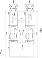
- FIG. 1 is a schematic illustrating a system 100 for handling data, according to one or more embodiments of the present disclosure.
- System 100 for handling data can operate according to an Ethernet networking standard, as will be understood by one of ordinary skill in the art.
- the system 100 can be a network switch.
- the system 100 includes a number of physical layer (PHY) circuits 102-1, ..., 102-N.
- Physical layer can refer to the physical layer of the Open System Interconnection Reference Model (OSI model), as will be appreciated by one of ordinary skill in the art.
- the PHY circuits 102-1, ..., 102-N can be individual chips, can be integrated on a single PHY chip, or can be integrated with the system 100 on a single chip such as a system-on-a-chip (SoC).
- SoC system-on-a-chip
- Each of the PHY circuits 102-1, ..., 102-N can include a number of ports 104-1, ..., 104-P respectively.
- each PHY circuit can include eight ports.
- the ports 104-1, ..., 104-P for each PHY 102-1, ..., 102-N can be connected to a number of physical mediums such as twisted pair, copper wire, optical fibers, etc. for communication of data outside of the system 100. Such data communication can correspond to the data link layer of the OSI model.
- Each of the PHY circuits 102-1, ..., 102-N can include a number of channels 106-1, ..., 106-M respectively.
- the number of channels 106-1, ..., 106-M for each PHY circuit 102-1, .., 102-N can be the same or different than the number of ports for each PHY circuit 102-1, ..., 102-N.
- the PHY circuits 102-1, ..., 102-N can be connected to a number of media access control (MAC) circuits 108 via a number of interfaces 110-1, .. ., 110-N.
- MAC media access control
- Figure 1 illustrates the MAC circuits 108 as a single chip, embodiments are not so limited and the MAC circuits 108 can include more than one chip.
- the MAC circuits 108 can include a number of channels 107. In one or more embodiments, the number of channels 107 included in the MAC circuits 108 can be equal to the number of channels 106-1, ..., 106-M included in the PHY circuits 102-1, ..., 102-N in the system 100.
- the channels 107 included in the MAC circuits 108 and the channels 106-1, ..., 106-M included in the PHY circuits 102-1, .., 102-N can be used to communicate data between the MAC circuits 108 and the PHY 102-1, .. , 102-N circuits via the interfaces 110-1, ..., 110-N.
- the interfaces 110-1, ..., 110-N can be multiplexed serial media independent interfaces (MSMII).
- MII media independent interface
- Each MSMII 110-1, ..., 110-N can include a first differential signal communicated via a first pair of conductors 116-1, ..., 116-N to transmit data from the PHY circuits 102-1, ..., 102-N to the MAC circuits 108 and a second differential signal communicated via a second pair of conductors 117-1, ..., 117-N to transmit data from the MAC circuits 108 to the PHY circuits 102-1, ..., 102-N.
- Each differential signal can include a positive polarity portion and a negative polarity portion. Accordingly, each MSMII 110-1, ..., 110-N can include four pins that correlate to (e.g., can be used to transmit and/or receive) the four signals (e.g., the positive and negative polarity portions of the two differential signals).
- the differential signals can be low voltage (e.g., 3.3 volt) signals conveyed with positive logic such that a signal is at a logic "high” (e.g., "1") when the positive signal of the differential pair is at a voltage level greater than the negative signal of the differential pair.
- the signal can be at a logic "low” (e.g., "0") when the positive signal of the differential pair is at a voltage less than the negative signal of the differential pair.
- the PHY circuits 102-1, ..., 102-N, the MAC circuits 108, and the interfaces 110-1, ..., 110-N can be configured to operate at a number of rates.
- the PHY circuits 102-1, ..., 102-N and the MAC circuits 108 can be configured to operate at a first rate (e.g., 10 Mbps) and the interfaces 110-1, ..., 110-N can be configured to operate at a second rate (e.g., 100 Mbps).
- the PHY circuits 102-1, ..., 102-N, MAC circuits 108, and interfaces 110-1, ...., 110-N can operate at the same rate or at different rates from one another.
- the PHY circuits 102-1, ..., 102-N and the MAC circuits 108 can be configured to operate at a first rate and the interfaces 110-1, .., 110-N can be configured to operate at a second rate greater than the first rate.
- the system 100 can include a management data clock (MDC) signal 112 for communicating data via a management interface between the MAC circuits 108 and the PHY circuits 102-1, ..., 102-N.
- the management data clock can be a reference clock for the MAC circuits 108.
- the reference clock for the MAC circuits 108 can be used to generate the second differential signal and/or used to generate timing of the first differential signal.
- the system 100 can also include a management data input / output (MDIO) signal 114 for communicating via the management interface between the MAC circuits 108 and the PHY circuits 102-1, ..., 102-N.
- the PHY circuits 102-1, ..., 102-N can be configured to synchronize data communications with a clock signal (e.g., management data clock signal 112) from the MAC circuits 108.
- a clock signal e.g., management data clock signal 112
- FIG. 2 is a schematic illustrating portions of a system 200 for handling data, according to one or more embodiments of the present disclosure.
- the system 200 can include a number of PHY circuits 202-1, ..., 202-N, a number of MAC circuits 208-1, ..., 208-N, and a number of interfaces (e.g., MSMII) 210.
- the system 200, PHY circuits 202-1, ..., 202-N, MAC circuits 208-1, ..., 208-N, and interfaces 210 can be analogous to the system 100, PHY circuits 102-1, ..., 102-N, MAC circuits 108, and interfaces 110-1, . . ., 110-N illustrated in Figure 1 respectively.
- the system 200 illustrated in Figure 2 includes additional detail with respect to the interfaces 210.
- the interfaces 210 can include interface components 222-1 and 222-2 associated with the MAC circuits 208-1, ..., 208-N and the PHY circuits 202-1, ..., 202-N respectively.
- the interface components 222-1, 222-2 can function as transmit components and/or receive components of the interfaces 210. For example, when the PHY circuits 202-1, .
- the interface component 222-2 associated with the PHY circuits 202-1, ..., 202-N can function as a transmit component and the interface component 222-1 associated with the MAC circuits 208-1, ..., 208-N can function as a receive component.
- the interface component 222-1 can function as a transmit component and the interface component 222-2 can function as a receive component.
- Each interface component 222-1, 222-2 can include a state machine 218-1, 218-2 and a serializer / deserializer (SerDes) circuit 220-1, 220-2 respectively.
- the interfaces 210 and/or interface components 222-1, 222-2 can include additional circuits, components, and/or functionality not specifically illustrated in Figure 2 .
- the interfaces 210 can be configured to encode data transmitted via the interfaces 210 (e.g., using a state machine 218-1, 218-2).
- the data can be encoded using 8b/10b encoding into groups of data symbols. At least one data symbol from each of the number of channels can be included in a group of data symbols.
- a group of eight data symbols can include one data symbol from each of the eight channels.
- a group of eight data symbols can include at least one symbol from each channel plus a number of repeated data symbols up to eight data symbols total.
- the interfaces can add one or more control sets to a group of data symbols of encoded data (e.g., using a state machine 218-1, 218-2). For example, one control set can be added for every eight data symbols.
- the control set can include two symbols including a particular starter symbol indicating that the interfaces 210 are operating as multiplexed serial media independent interfaces and a channel symbol indicating status and the number of channels being communicated (e.g., one control set including two symbols can be added for every eight data symbols).
- the particular starter symbol can be unique to multiplexed serial media independent interfacing.
- the particular channel symbol can include eight defined bits. A first bit can indicate whether a receive component has established a valid link with the interface. A second bit can indicate whether a remote interface is operational. A third bit can indicate whether a local device is operational. A fourth bit can be reserved for other indications. Thus, the first four bits can indicate status. However, embodiments are not limited to a particular ordering of the bits.
- the channel symbol can include four additional bits that can be used to indicate the number of channels being communicated. For embodiments including one control set per eight data symbols, a data rate "gear ratio" of 1.25:1 can be provided.
- eight channels of data can be encoded, have a control set added, and be multiplexed from eight channels at 100 Mbps to a serial stream data rate of 1.25 Gbps.
- Table 1 illustrates an example of eight channels of data having an original rate of 100 Mbps encoded with 8b/10b encoding and a serial stream resulting from multiplexing the eight channels.
- the first eight rows of Table 1 illustrate eight channels having data symbols "S" denoted by a first number indicating the channel number (e.g., from 0 to 7) and a subscript number indicating the symbol number within the channel (e.g., from 1 to 8).
- the ninth row illustrates the multiplexed serial data stream including control symbols "C" and data symbols "S".
- An example of eight channels of data having an original rate of 10 Mbps encoded with 8b/10b encoding and a serial stream resulting from multiplexing the eight channels can be similar to that illustrated in the example associated with Table 1 and an original 100 Mbps stream, except that each symbol can be repeated ten times to bring the overall serial stream to 1 Gbps.
- Multiplexing of the encoded data can be achieved with time division multiplexing (e.g., using a SerDes 220-1, 220-2) of encoded data from the number of channels.
- time division multiplexing e.g., using a SerDes 220-1, 220-2
- the interfaces 210 can multiplex data from a number of channels (e.g., channels 106-1, ..., 106-M, 107 illustrated in Figure 1 ) at the first rate to a serial data stream at the second rate.
- the interfaces 210 can multiplex data from the PHY circuits 202-1, ..., 202-N and the MAC circuits 208-1, ..., 208-N, which can operate at 10/100 Mbps, to a serial stream at 1.25 Gbps.
- a transmit component (e.g., component 222-2) of the interfaces 210 can be configured to multiplex data (e.g., via SerDes 220-2) for transmit circuits (e.g., PHY circuits 202-1, ..., 202-N) operating more than one channel at a rate less than a rate of the interfaces 210.
- transmit circuits e.g., PHY circuits 202-1, ..., 202-N
- the transmit component can multiplex data from a first rate (e.g., the rate of the transmit circuit, such as the PHY circuits 202-1, ..., 202-N and/or the MAC circuits 208-1, ..., 208-N when either is transmitting) to a second rate (e.g., the rate of the interfaces 210) by transmitting the control set followed by a first data symbol from a first channel and a second data symbol from a second channel, etc. at the second rate.
- the transmit circuit can transmit a control set and eight data symbols (e.g., one from each of eight channels) multiplexed from 100 Mbps to create a frame to be transmitted in a serial stream via the interfaces 210 at 1.25 Gbps.
- the control set can include a particular starter symbol and a channel symbol as described herein.
- a receive component (e.g., component 222-1) of the interfaces 210 can be configured to demultiplex the received encoded data from the serial stream at the second rate to a number of channels at the first rate in response to the control set including the particular starter symbol indicating that the serial stream is a multiplexed serial media independent interface transmission and the channel symbol indicating status and transmission of more than one channel (multiplexed into a serial stream).
- a transmit component (e.g., component 222-2) of the interfaces 210 can be configured to serialize data (e.g., via SerDes 220-2) for transmit circuits (e.g., PHY circuits 202-1, ..., 202-N) operating one channel at a rate less than a rate of the interfaces 210.
- the transmit component can serialize data from a first rate (e.g., the rate of the transmit circuit) to a second rate (e.g., the rate of the interfaces 210) by repeating data (e.g., data symbols when the data being transmitted is encoded) a sufficient number of times such that a frame of data can be transmitted at the second rate.
- the transmit circuit can repeat a data symbol ten times from a transmit circuit at 100 Mbps to create a frame to be transmitted via the interfaces 210 at a rate of at least 1 Gbps.
- a receive component (e.g., component 222-1) of the interfaces 210 can be configured to deserialize the received encoded data from the serial stream at the second rate to one channel at the first rate in response to the control set including the particular starter symbol indicating that the serial stream is a multiplexed stream serial media independent interface transmission and the channel symbol indicating status and transmission of a single channel (in a serial stream).
- a transmit component (e.g., component 222-2) of the interfaces 210 can be configured to pass data through the interfaces 210 without multiplexing for transmit circuits (e.g., PHY circuits 202-1, ..., 202-N) operating a single channel at a rate equal to a rate of the interfaces 210.
- transmit circuits e.g., PHY circuits 202-1, ..., 202-N
- a transmit component e.g., component 222-2
- a transmit component can pass data from the PHY circuits 202-1, ..., 202-N to the MAC circuits 208-1, ..., 208-N via the interfaces 210 without multiplexing the data.
- a receive component (e.g., component 222-1) of the interfaces 210 can be configured to receive the data from the serial stream without demultiplexing in response to an absence of the particular starter symbol with the received data.
- the received serial data stream can be at a rate equivalent to a rate of the PHY circuit 202-1, ..., 202-N, the MAC circuit 208-1, ..., 208-N, and the interfaces 210.
Description
- In network devices (e.g., switches), production cost may be impacted significantly by the number of conductors (e.g., pins) used on integrated circuits (ICs) within a network device, and the number of signals routed on circuits (e.g., printed circuit boards (PCBs)). For example, a Media Independent Interface (Mil) including 24 ports operating at 10 megabits per second (Mbps) and/or 100 Mbps (10/100) Ethernet interfacing between a media access control (MAC) circuit and physical layer (PHY) circuit may include 384 pins. Other interfaces may operate at one gigabit per second (Gbps) or faster.
- Newer interfaces that reduce the number of pins have been developed such as the Reduced Media Independent Interface (RMII), Serial Media Independent Interface (SMII), and Serial Gigabit Media Independent Interface (SGMII). An RMII may use eight pins per port such that a 24 port switch could include 192 pins for interfacing between the MAC and the PHY circuits. An SMII may include four pins per port, so a 24 port switch could include 96 pins, plus four additional clock signals. An SGMII (e.g., 10/100/1000 Mbps) may be designed for single ports and use four pins per PHY resulting in 96 pins for 24 ports.
- A MAC may be located within a semiconductor device or "chip." One function of a MAC may be to communicate data over a physical medium (e.g., an optical fiber or a conductive wire). In other words, the MAC may be the interface between the physical medium and the higher layer functions in a device (e.g., an operating system, routing function, etc.). The MAC may communicate with other devices (e.g., other PHY circuits) located on remote chips through the use of a serializer/deserializer (SerDes) device that converts parallel data from the MAC into serial data for transmission over the physical medium. The SerDes may also convert received serial data into parallel data for use with its associated MAC.
-
CN101437035 A relates to a data communication method and Ethernet equipment. The method ofCN101437035 A comprises: a physical layer PHY chip compounds n paths of first speed physical layer data received from n interfaces into one path of second speed data and sends the second speed data to an MAC chip; n is a natural number greater than 1; and when receiving the second speed data from the PHY chip, the MAC chip decomposes the second speed data into the n paths of first speed data. The technical proposal of the invention enables a single MAC chip in the Ethernet equipment to support larger port density and reduces the cost for accessing a broadband to user application. -
-
Figure 1 is a schematic illustrating a system for handling data, according to one or more embodiments of the present disclosure. -
Figure 2 is a schematic illustrating portions of a system for handling data, according to one or more embodiments of the present disclosure. - Systems, methods, and devices are provided for a multiplexed serial media independent interface. One system for handling data includes a physical layer (PHY) circuit operating at a first rate including a number of ports, a media access control (MAC) circuit operating at the first rate including a number of ports, and a multiplexed serial media independent interface between the MAC circuit and the PHY circuit operating at a second rate, which is greater than the first rate. The interface includes a number of conductors and is configured to communicate data between the MAC circuit and the PHY circuit via four conductors per up to eight ports of the PHY circuit.
- The figures herein follow a numbering convention in which the first digit or digits correspond to the drawing figure number and the remaining digits identify an element or component in the drawing. Similar elements or components between different figures may be identified by the use of similar digits. For example, 108 may reference element "08" in
Figure 1 , and a similar element may be referenced as 208-1, ..., 208-N inFigure 2 . As will be appreciated, elements shown in the various embodiments herein can be added, exchanged, and/or eliminated so as to provide a number of additional embodiments of the present disclosure. In addition, as will be appreciated, the proportion and the relative scale of the elements provided in the figures are intended to illustrate the embodiments of the present disclosure, and should not be taken in a limiting sense. As used herein, "a number of" something can refer to one or more such things. - As used herein, the designators "N," "M," and "P," particularly with respect to reference numerals in the drawings, indicate that a number of the particular feature so designated can be included with one or more embodiments of the present invention. The designators can represent the same or different numbers of the particular features.
- One or more embodiments of the present disclosure can provide a system for communicating data serially between one or more MAC circuits and a corresponding one or more PHY circuits at rates faster than a rate at which the PHY circuit communicates data external to the system. For example, the PHY circuit and/or the MAC circuit may operate at rates of 10 or 100 Mbps and an interface between the PHY circuit and the MAC circuit can communicate data at a rate of at least 1000 Mbps.
- The present disclosure can provide for such communication between a Multiport MAC (MMAC) circuit and a Multiport PHY (MPHY) circuit using four conductors (e.g., pins) per up to eight ports and/or channels for the PHY circuit and/or the MAC circuit. Significantly reducing the number of pins (e.g., as compared to some previous approaches) can reduce power consumption and cost and can improve layout of a system by reducing the number of signals used between circuits. In one or more embodiments such a system can be a network switch.
- Embodiments of the present disclosure may include systems for handling data. Such systems can be a network device such as a switch. Such network devices can include a processor in communication with a memory and may include network chips having hardware logic (e.g., in the form of application specific integrated circuits (ASICs)), associated with a number of network ports. Devices in a network are not limited to a number of ports, network chips and/or the type or size of processor or memory resources.
- As one of ordinary skill in the art will appreciate, each network device in a network can be physically associated with a port of a switch to which it is connected. Information in the form of packets can be passed through the network. Users can physically connect to the network through ports on the network device (e.g., switch). Data frames, or packets, can be transferred between network devices by means of a network device's (e.g., switch's) logic link control (LLC)/ media access control (MAC) circuitry, or "engines", as associated with ports on a network device. A network switch forwards packets received from a transmitting network device to a destination network device based on the header information in received packets. A network device can also forward packets from a given network to other networks through ports on one or more other network devices. As the reader will appreciate an Ethernet network is described herein. However, embodiments are not limited to use in an Ethernet network, and may be equally well suited to other network types (e.g., asynchronous transfer mode (ATM) networks, etc).
- As used herein, a network can provide a communication system that links two or more computers and peripheral devices, allows users to access resources on other computers, and exchange messages with other users. A network allows users to share resources on their own systems with other network users and to access information on centrally located systems or systems that are located at remote offices. It may provide connections to the Internet or to the networks of other organizations. Users may interact with network-enabled software applications to make a network request, such as to get a file or print on a network printer. Applications may also communicate with network management software, which can interact with network hardware to transmit information between devices on the network.
-
Figure 1 is a schematic illustrating asystem 100 for handling data, according to one or more embodiments of the present disclosure.System 100 for handling data can operate according to an Ethernet networking standard, as will be understood by one of ordinary skill in the art. In one or more embodiments, thesystem 100 can be a network switch. Thesystem 100 includes a number of physical layer (PHY) circuits 102-1, ..., 102-N. "Physical layer" can refer to the physical layer of the Open System Interconnection Reference Model (OSI model), as will be appreciated by one of ordinary skill in the art. The PHY circuits 102-1, ..., 102-N can be individual chips, can be integrated on a single PHY chip, or can be integrated with thesystem 100 on a single chip such as a system-on-a-chip (SoC). - Each of the PHY circuits 102-1, ..., 102-N can include a number of ports 104-1, ..., 104-P respectively. For example, each PHY circuit can include eight ports. The ports 104-1, ..., 104-P for each PHY 102-1, ..., 102-N can be connected to a number of physical mediums such as twisted pair, copper wire, optical fibers, etc. for communication of data outside of the
system 100. Such data communication can correspond to the data link layer of the OSI model. Each of the PHY circuits 102-1, ..., 102-N can include a number of channels 106-1, ..., 106-M respectively. The number of channels 106-1, ..., 106-M for each PHY circuit 102-1, .., 102-N can be the same or different than the number of ports for each PHY circuit 102-1, ..., 102-N. - The PHY circuits 102-1, ..., 102-N can be connected to a number of media access control (MAC)
circuits 108 via a number of interfaces 110-1, .. ., 110-N. AlthoughFigure 1 illustrates theMAC circuits 108 as a single chip, embodiments are not so limited and theMAC circuits 108 can include more than one chip. TheMAC circuits 108 can include a number ofchannels 107. In one or more embodiments, the number ofchannels 107 included in theMAC circuits 108 can be equal to the number of channels 106-1, ..., 106-M included in the PHY circuits 102-1, ..., 102-N in thesystem 100. Thechannels 107 included in theMAC circuits 108 and the channels 106-1, ..., 106-M included in the PHY circuits 102-1, .., 102-N can be used to communicate data between theMAC circuits 108 and the PHY 102-1, .. , 102-N circuits via the interfaces 110-1, ..., 110-N. - The interfaces 110-1, ..., 110-N can be multiplexed serial media independent interfaces (MSMII). In general, a media independent interface (MII) can be used to connect different types of PHY circuits to a common MAC circuit. Each MSMII 110-1, ..., 110-N can include a first differential signal communicated via a first pair of conductors 116-1, ..., 116-N to transmit data from the PHY circuits 102-1, ..., 102-N to the
MAC circuits 108 and a second differential signal communicated via a second pair of conductors 117-1, ..., 117-N to transmit data from theMAC circuits 108 to the PHY circuits 102-1, ..., 102-N. Each differential signal can include a positive polarity portion and a negative polarity portion. Accordingly, each MSMII 110-1, ..., 110-N can include four pins that correlate to (e.g., can be used to transmit and/or receive) the four signals (e.g., the positive and negative polarity portions of the two differential signals). - The differential signals can be low voltage (e.g., 3.3 volt) signals conveyed with positive logic such that a signal is at a logic "high" (e.g., "1") when the positive signal of the differential pair is at a voltage level greater than the negative signal of the differential pair. The signal can be at a logic "low" (e.g., "0") when the positive signal of the differential pair is at a voltage less than the negative signal of the differential pair.
- The PHY circuits 102-1, ..., 102-N, the
MAC circuits 108, and the interfaces 110-1, ..., 110-N can be configured to operate at a number of rates. For example, the PHY circuits 102-1, ..., 102-N and theMAC circuits 108 can be configured to operate at a first rate (e.g., 10 Mbps) and the interfaces 110-1, ..., 110-N can be configured to operate at a second rate (e.g., 100 Mbps). The PHY circuits 102-1, ..., 102-N,MAC circuits 108, and interfaces 110-1, ...., 110-N can operate at the same rate or at different rates from one another. In one or more embodiments, the PHY circuits 102-1, ..., 102-N and theMAC circuits 108 can be configured to operate at a first rate and the interfaces 110-1, .., 110-N can be configured to operate at a second rate greater than the first rate. - The
system 100 can include a management data clock (MDC) signal 112 for communicating data via a management interface between theMAC circuits 108 and the PHY circuits 102-1, ..., 102-N. The management data clock can be a reference clock for theMAC circuits 108. In one or more embodiments, the reference clock for theMAC circuits 108 can be used to generate the second differential signal and/or used to generate timing of the first differential signal. Thesystem 100 can also include a management data input / output (MDIO) signal 114 for communicating via the management interface between theMAC circuits 108 and the PHY circuits 102-1, ..., 102-N. The PHY circuits 102-1, ..., 102-N can be configured to synchronize data communications with a clock signal (e.g., management data clock signal 112) from theMAC circuits 108. -
Figure 2 is a schematic illustrating portions of asystem 200 for handling data, according to one or more embodiments of the present disclosure. Thesystem 200 can include a number of PHY circuits 202-1, ..., 202-N, a number of MAC circuits 208-1, ..., 208-N, and a number of interfaces (e.g., MSMII) 210. Thesystem 200, PHY circuits 202-1, ..., 202-N, MAC circuits 208-1, ..., 208-N, and interfaces 210 can be analogous to thesystem 100, PHY circuits 102-1, ..., 102-N,MAC circuits 108, and interfaces 110-1, . . ., 110-N illustrated inFigure 1 respectively. - The
system 200 illustrated inFigure 2 includes additional detail with respect to theinterfaces 210. Theinterfaces 210 can include interface components 222-1 and 222-2 associated with the MAC circuits 208-1, ..., 208-N and the PHY circuits 202-1, ..., 202-N respectively. The interface components 222-1, 222-2 can function as transmit components and/or receive components of theinterfaces 210. For example, when the PHY circuits 202-1, . .., 202-N transmit data to the MAC circuits 208-1, ..., 208-N, the interface component 222-2 associated with the PHY circuits 202-1, ..., 202-N can function as a transmit component and the interface component 222-1 associated with the MAC circuits 208-1, ..., 208-N can function as a receive component. Likewise, when the MAC circuits 208-1, ..., 208-N transmit data to the PHY circuits 202-1, ..., 202-N, the interface component 222-1 can function as a transmit component and the interface component 222-2 can function as a receive component. - Each interface component 222-1, 222-2 can include a state machine 218-1, 218-2 and a serializer / deserializer (SerDes) circuit 220-1, 220-2 respectively. The
interfaces 210 and/or interface components 222-1, 222-2 can include additional circuits, components, and/or functionality not specifically illustrated inFigure 2 . - In one or more embodiments, the
interfaces 210 can be configured to encode data transmitted via the interfaces 210 (e.g., using a state machine 218-1, 218-2). For example, the data can be encoded using 8b/10b encoding into groups of data symbols. At least one data symbol from each of the number of channels can be included in a group of data symbols. For embodiments using eight channels, a group of eight data symbols can include one data symbol from each of the eight channels. For embodiments using fewer than eight channels, a group of eight data symbols can include at least one symbol from each channel plus a number of repeated data symbols up to eight data symbols total. The interfaces can add one or more control sets to a group of data symbols of encoded data (e.g., using a state machine 218-1, 218-2). For example, one control set can be added for every eight data symbols. In one or more embodiments, the control set can include two symbols including a particular starter symbol indicating that theinterfaces 210 are operating as multiplexed serial media independent interfaces and a channel symbol indicating status and the number of channels being communicated (e.g., one control set including two symbols can be added for every eight data symbols). - The particular starter symbol can be unique to multiplexed serial media independent interfacing. The particular channel symbol can include eight defined bits. A first bit can indicate whether a receive component has established a valid link with the interface. A second bit can indicate whether a remote interface is operational. A third bit can indicate whether a local device is operational. A fourth bit can be reserved for other indications. Thus, the first four bits can indicate status. However, embodiments are not limited to a particular ordering of the bits. The channel symbol can include four additional bits that can be used to indicate the number of channels being communicated. For embodiments including one control set per eight data symbols, a data rate "gear ratio" of 1.25:1 can be provided. For example, encoding data that has an original rate of 100 Mbps, using 8b/10b encoding, can yield an effective rate of 125 Mbps ((100 * 10)/8 = 125). Thus, eight channels of data can be encoded, have a control set added, and be multiplexed from eight channels at 100 Mbps to a serial stream data rate of 1.25 Gbps.
- Table 1 illustrates an example of eight channels of data having an original rate of 100 Mbps encoded with 8b/10b encoding and a serial stream resulting from multiplexing the eight channels. The first eight rows of Table 1 illustrate eight channels having data symbols "S" denoted by a first number indicating the channel number (e.g., from 0 to 7) and a subscript number indicating the symbol number within the channel (e.g., from 1 to 8). The ninth row illustrates the multiplexed serial data stream including control symbols "C" and data symbols "S".
TABLE 1 S01 S02 ··· S08 S11 S12 ··· S18 S21 S22 ··· S28 S31 S32 ··· S38 S41 S42 ··· S48 S51 S52 ··· S58 S61 S62 ··· S68 S71 S72 ··· S78 C1 C2 S01 S11 S21 S31 S41 S51 S61 S71 C1 C2 S12 S22 ··· S58 S68 S78 - An example of eight channels of data having an original rate of 10 Mbps encoded with 8b/10b encoding and a serial stream resulting from multiplexing the eight channels can be similar to that illustrated in the example associated with Table 1 and an original 100 Mbps stream, except that each symbol can be repeated ten times to bring the overall serial stream to 1 Gbps.
- Multiplexing of the encoded data (e.g., including the added control sets) can be achieved with time division multiplexing (e.g., using a SerDes 220-1, 220-2) of encoded data from the number of channels. For embodiments in which the PHY circuits 202-1, ..., 202-N and/or MAC circuits 208-1, ..., 208-N operate at a first rate less than a second rate at which the
interfaces 210 operate and in which the PHY circuits 202-1, ..., 202-N include a number of ports (e.g., ports 104-1, ..., 104-P illustrated inFigure 1 ) greater than one, theinterfaces 210 can multiplex data from a number of channels (e.g., channels 106-1, ..., 106-M, 107 illustrated inFigure 1 ) at the first rate to a serial data stream at the second rate. For example, theinterfaces 210 can multiplex data from the PHY circuits 202-1, ..., 202-N and the MAC circuits 208-1, ..., 208-N, which can operate at 10/100 Mbps, to a serial stream at 1.25 Gbps. - A transmit component (e.g., component 222-2) of the
interfaces 210 can be configured to multiplex data (e.g., via SerDes 220-2) for transmit circuits (e.g., PHY circuits 202-1, ..., 202-N) operating more than one channel at a rate less than a rate of theinterfaces 210. The transmit component can multiplex data from a first rate (e.g., the rate of the transmit circuit, such as the PHY circuits 202-1, ..., 202-N and/or the MAC circuits 208-1, ..., 208-N when either is transmitting) to a second rate (e.g., the rate of the interfaces 210) by transmitting the control set followed by a first data symbol from a first channel and a second data symbol from a second channel, etc. at the second rate. For example, the transmit circuit can transmit a control set and eight data symbols (e.g., one from each of eight channels) multiplexed from 100 Mbps to create a frame to be transmitted in a serial stream via theinterfaces 210 at 1.25 Gbps. The control set can include a particular starter symbol and a channel symbol as described herein. - A receive component (e.g., component 222-1) of the
interfaces 210 can be configured to demultiplex the received encoded data from the serial stream at the second rate to a number of channels at the first rate in response to the control set including the particular starter symbol indicating that the serial stream is a multiplexed serial media independent interface transmission and the channel symbol indicating status and transmission of more than one channel (multiplexed into a serial stream). - A transmit component (e.g., component 222-2) of the
interfaces 210 can be configured to serialize data (e.g., via SerDes 220-2) for transmit circuits (e.g., PHY circuits 202-1, ..., 202-N) operating one channel at a rate less than a rate of theinterfaces 210. The transmit component can serialize data from a first rate (e.g., the rate of the transmit circuit) to a second rate (e.g., the rate of the interfaces 210) by repeating data (e.g., data symbols when the data being transmitted is encoded) a sufficient number of times such that a frame of data can be transmitted at the second rate. For example, the transmit circuit can repeat a data symbol ten times from a transmit circuit at 100 Mbps to create a frame to be transmitted via theinterfaces 210 at a rate of at least 1 Gbps. - A receive component (e.g., component 222-1) of the
interfaces 210 can be configured to deserialize the received encoded data from the serial stream at the second rate to one channel at the first rate in response to the control set including the particular starter symbol indicating that the serial stream is a multiplexed stream serial media independent interface transmission and the channel symbol indicating status and transmission of a single channel (in a serial stream). - A transmit component (e.g., component 222-2) of the
interfaces 210 can be configured to pass data through theinterfaces 210 without multiplexing for transmit circuits (e.g., PHY circuits 202-1, ..., 202-N) operating a single channel at a rate equal to a rate of theinterfaces 210. For example, for embodiments including theinterfaces 210 and the PHY circuits 202-1, ..., 202-N and the MAC circuits 208-1, ..., 208-N operating at a rate of at least one Gbps, a transmit component (e.g., component 222-2) can pass data from the PHY circuits 202-1, ..., 202-N to the MAC circuits 208-1, ..., 208-N via theinterfaces 210 without multiplexing the data. - A receive component (e.g., component 222-1) of the
interfaces 210 can be configured to receive the data from the serial stream without demultiplexing in response to an absence of the particular starter symbol with the received data. The received serial data stream can be at a rate equivalent to a rate of the PHY circuit 202-1, ..., 202-N, the MAC circuit 208-1, ..., 208-N, and theinterfaces 210. - Although specific embodiments have been illustrated and described herein, those of ordinary skill in the art will appreciate that an arrangement calculated to achieve the same results can be substituted for the specific embodiments shown. This disclosure is intended to cover adaptations or variations of one or more embodiments of the present disclosure. It is to be understood that the above description has been made in an illustrative fashion, and not a restrictive one. Combination of the above embodiments, and other embodiments not specifically described herein will be apparent to those of skill in the art upon reviewing the above description. The scope of the one or more embodiments of the present disclosure includes other applications in which the above structures and methods are used. Therefore, the scope of one or more embodiments of the present disclosure should be determined with reference to the appended claims.
- In the foregoing Detailed Description, some features are grouped together in a single embodiment for the purpose of streamlining the disclosure. This method of disclosure is not to be interpreted as reflecting an intention that the disclosed embodiments of the present disclosure have to use more features than are expressly recited in each claim. Rather, as the following claims reflect, inventive subject matter lies in less than all features of a single disclosed embodiment. Thus, the following claims are hereby incorporated into the Detailed Description, with each claim standing on its own as a separate embodiment.
Claims (13)
- A system (100, 200) for handling data, comprising:a physical layer, PHY, circuit (102-1, 102-N, 202-1, 202-N) operating at a first rate, wherein the PHY circuit (102-1, 102-N, 202-1, 202-N) includes a number of ports (104-1, 104-P);a media access control, MAC circuit (108, 208-1, 208-N) operating at the first rate, wherein the MAC circuit (108, 208-1, 208-N) includes a number of ports; anda multiplexed serial media independent interface (110-1, 110-N, 210) between the MAC circuit (108, 208-1, 208-N) and the PHY circuit (102-1, 102-N, 202-1, 202-N) operating at a second rate greater than the first rate, wherein the interface (110-1, 110-N, 210) includes a number of conductors;wherein the interface (110-1, 110-N, 210) is configured to communicate data between the MAC circuit (108, 208-1, 208-N) and the PHY circuit (102-1, 102-N, 202-1, 202-N) via four conductors per up to eight ports (104-1, 104-P) of the PHY circuit (102-1, 102-N, 202-1, 202-N); characterized in that:the interface (110-1,110-N, 210) is configured to: encode (218-1, 218-2) the data communicated via the interface (110-1, 110-N, 21 O);add (218-1, 218-2) one or more control sets to the encoded data; wherein the one or more control sets include a particular starter symbol indicating that the interface between the MAC circuit and the PHY circuit is operating as a multiplexed serial media independent interface and a channel symbol indicating a status and a number of channels (106-1, 106-M) being communicated; andtime division multiplex (220-1, 220-2) the encoded data from the number of channels (106-1, 106-M) at the first rate to a serial data stream at the second rate when the number of ports (104-1, 104-P) is greater than one.
- The system (100, 200) of claim 1, wherein:
the interface (110-1, 110-N, 210) includes a transmit component (222-1, 222-2) and a receive component (222-1, 222-2) - The system (100, 200) of claim 2, wherein the receive component (222-1, 222-2) is configured to demultiplex (220-1, 220-2) the encoded data from the serial stream at the second rate to the number of channels (106-1, 106-M) at the first rate in response to the one or more control sets including the particular starter symbol and the channel symbol indicating status and the number of channels (106-1, 106-M) in the serial data stream.
- The system (100, 200) of claim 3, wherein the first rate Is 100 megabits per second and the second rate is 1.25 gigabits per second.
- The system (100, 200) of claim 2, wherein the receive component (222-1, 222-2) is configured to deserialize (220-1, 220-2) the encoded data from the serial stream at the second rate to one channel (106-1, 106-M) at the first rate in response to the one or more control sets including the particular starter symbol and the channel symbol indicating status and the number of channels (106-1, 106-M) comprises one channel (106-1, 106-M).
- The system (100, 200) of claim 2, wherein: the particular channel symbol comprises eight bits including:a first bit indicating whether the receive component (222-1, 222-2) has established a valid link; operational;a second bit indicating whether a remote interface isa third bit indicating whether a local device is operational;a fourth bit reserved; andfour bits indicating the number of channels (106-1, 106-M).
- The system (100, 200) of claim 1, wherein the interface (110-1, 110-N, 210) is configured to add one control set per eight data symbols; and
wherein the interface (110-1, 110-N, 210) is configured to encode (218-1, 218-2) the data using 8b/10b encoding. - The system (100, 200) of claim 7, wherein the eight data symbols include at least one data symbol from each of the number of channels (106-1, 106-M); and
wherein the eight data symbols include at least one data symbol from a particular channel (106-1, 106-M) of the number of channels (106-1, 106-M) and a repeat of the at least one symbol from the particular channel (106-1, 106-M) when the number of channels (106-1, 106-M) is more than two and less than eight. - The system (100, 200) of claim 1, wherein:the MAC circuit (108, 208-1, 208-N) and the PHY circuit (102-1, 102-N, 202-1, 202-N) are configured to operate at the second rate;the interface (110-1, 110-N, 210) includes a transmit component (222-1, 222-2) and a receive component (222-1, 222-2);the transmit component (222-1, 222-2) is configured to transmit the data without multiplexing; andthe receive component (222-1, 222-2) is configured to receive the data without demultiplexing in response to an absence of a particular starter symbol.
- The system (100, 200) of claim 9, wherein the second rate is at least one gigabit per second.
- The system (100, 200) of claim 1, wherein the four conductors (116-1, 116-N, 117-1, 117-N) communicate two differential signals including:a first differential signal to transmit the data from the PHY circuit (102-1, 102-N, 202-1, 202-N) to the MAC circuit (108, 208-1, 208-N); anda second differential signal to transmit data from the MAC circuit (108, 208-1, 208-N) to the PHY circuit (102-1, 102-N, 202-1, 202-N).
- The system (100, 200) of claim 10, wherein the system (100, 200) includes:a management data clock signal (112) for communicating via a management interface between the MAC circuit (108, 208-1, 208-N) and the PHY circuit (102-1, 102-N, 202-1, 202-N);a management data input I output signal (114) for communicating via a the management interface between the MAC circuit (108, 208-1, 208-N) and the PHY circuit (102-1, 102-N, 202-1, 202-N); andwherein the PHY circuit (102-1, 102-N, 202-1, 202-N) is configured to synchronize data transmissions with the management data clock signal (112) from the MAC circuit (108, 208-1, 208-N).
- A method for handling data, comprising:operating a physical layer, PHY, circuit (102-1, 102-N, 202-1, 202-N) at a first rate, wherein the PHY circuit (102-1, 102-N, 202-1, 202-N) includes a number of ports (104-1, 104-P);operating a media access control, MAC, circuit (108, 208-1, 208-N) at the first rate; andcommunicating data with a multiplexed serial media independent interface (110-1, 110-N, 210) including a number of conductors between the MAC circuit (108, 208-1, 208-N) and the PHY circuit (102-1, 102-N, 202-1, 202-N) at a second rate greater than the first rate;
the number of conductors comprising four conductors per up to eight ports (104-1, 104-P) of the PHY circuit (102-1, 102-N, 202-1, 202-N); characterized in that the method comprises:encoding (218-1, 218-2) the data communicated via the interface (110-1, 110-N, 210);adding (218-1, 218-2) one or more control sets to the encoded data, wherein the one or more control sets include a particular starter symbol indicating that the interface between the MAC circuit and the PHY circuit is operating as a multiplexed serial media independent interface and a channel symbol indicating a status and a number of channels (106-1, 106-M) being communicated; andtime division multiplexing (220-1, 220-2) the encoded data from the number of channels at the first rate to a serial data stream at the second rate when the number of ports (104-1, 104-P) is greater than one.
Applications Claiming Priority (1)
| Application Number | Priority Date | Filing Date | Title |
|---|---|---|---|
| PCT/US2010/036831 WO2011152818A1 (en) | 2010-06-01 | 2010-06-01 | Multiplexed serial media independent interface |
Publications (3)
| Publication Number | Publication Date |
|---|---|
| EP2577945A1 EP2577945A1 (en) | 2013-04-10 |
| EP2577945A4 EP2577945A4 (en) | 2018-01-03 |
| EP2577945B1 true EP2577945B1 (en) | 2019-12-18 |
Family
ID=45066995
Family Applications (1)
| Application Number | Title | Priority Date | Filing Date |
|---|---|---|---|
| EP10852609.6A Active EP2577945B1 (en) | 2010-06-01 | 2010-06-01 | Multiplexed serial media independent interface |
Country Status (4)
| Country | Link |
|---|---|
| US (1) | US9071373B2 (en) |
| EP (1) | EP2577945B1 (en) |
| CN (1) | CN102907061B (en) |
| WO (1) | WO2011152818A1 (en) |
Families Citing this family (5)
| Publication number | Priority date | Publication date | Assignee | Title |
|---|---|---|---|---|
| KR101760001B1 (en) | 2012-03-23 | 2017-07-20 | 퀄컴 인코포레이티드 | Configurable multi-mode media independent interface |
| EP2829044A4 (en) | 2012-03-23 | 2015-11-25 | Qualcomm Inc | Multi-port serial media independent interface |
| US8964772B2 (en) * | 2012-10-09 | 2015-02-24 | Broadcom Corporation | Method for implementing a multi-chip module with a high-rate interface |
| EP2963899B1 (en) * | 2013-03-21 | 2018-09-12 | Huawei Technologies Co., Ltd. | Transmission apparatus, connecting mechanism and method |
| CN114514710A (en) * | 2019-07-25 | 2022-05-17 | 迈凌有限公司 | Multiple ports with different baud rates on a single serializer |
Family Cites Families (11)
| Publication number | Priority date | Publication date | Assignee | Title |
|---|---|---|---|---|
| US6269104B1 (en) * | 1998-04-21 | 2001-07-31 | Hewlett- Packard Company | Link control state machine for controlling a media access controller, a serial physical layer device and a media independent interface physical layer device |
| US6385208B1 (en) | 1998-06-02 | 2002-05-07 | Cisco Technology, Inc. | Serial media independent interface |
| US6865189B2 (en) * | 2001-03-22 | 2005-03-08 | Lsi Logic Corporation | Minimal latency serial media independent interface to media independent interface converter |
| KR100460149B1 (en) * | 2001-11-28 | 2004-12-08 | 주식회사 코어세스 | Apparatus and Method for arbitrating data transmission of devices based on SMII standard |
| US7042893B1 (en) * | 2001-12-05 | 2006-05-09 | Marvell International Ltd. | Serial media independent interface with double data rate |
| US20040125809A1 (en) | 2002-12-31 | 2004-07-01 | Jeng Jack Ing | Ethernet interface over ATM Cell, UTOPIA xDSL in single and multiple channels converter/bridge on a single chip and method of operation |
| KR100645518B1 (en) | 2004-12-29 | 2006-11-14 | 삼성전자주식회사 | Interface translation system and method between media access control device and phy device |
| US7835389B2 (en) * | 2006-09-20 | 2010-11-16 | Broadcom Corporation | Method and system for an extended range Ethernet line code using 4B/3B mapping |
| US7957283B2 (en) * | 2008-06-24 | 2011-06-07 | Lantiq Deutschland Gmbh | Multi-port ethernet transceiver |
| CN101437035A (en) * | 2008-12-18 | 2009-05-20 | 杭州华三通信技术有限公司 | Data communication method and Ethernet equipment |
| JP5248444B2 (en) * | 2009-08-11 | 2013-07-31 | ルネサスエレクトロニクス株式会社 | Serial communication device |
-
2010
- 2010-06-01 WO PCT/US2010/036831 patent/WO2011152818A1/en active Application Filing
- 2010-06-01 EP EP10852609.6A patent/EP2577945B1/en active Active
- 2010-06-01 US US13/697,101 patent/US9071373B2/en active Active
- 2010-06-01 CN CN201080067163.1A patent/CN102907061B/en active Active
Non-Patent Citations (1)
| Title |
|---|
| None * |
Also Published As
| Publication number | Publication date |
|---|---|
| CN102907061B (en) | 2015-09-09 |
| EP2577945A4 (en) | 2018-01-03 |
| US20130060979A1 (en) | 2013-03-07 |
| CN102907061A (en) | 2013-01-30 |
| EP2577945A1 (en) | 2013-04-10 |
| WO2011152818A1 (en) | 2011-12-08 |
| US9071373B2 (en) | 2015-06-30 |
Similar Documents
| Publication | Publication Date | Title |
|---|---|---|
| US10374782B2 (en) | Full duplex transmission method for high speed backplane system | |
| EP1738533B1 (en) | Transceiver with automatic configuration based on auto-negociation | |
| EP2887596B1 (en) | Network device and information transmission method | |
| EP2020104B1 (en) | Multiple fiber optic gigabit ethernet links channelized over single optical link | |
| CA2450825C (en) | Protocol independent transmission using a 10 gigabit attachment unit interface | |
| CN1203684C (en) | Crossbar integrated circuit with parallel channels for communication device | |
| EP2577945B1 (en) | Multiplexed serial media independent interface | |
| JP5882530B2 (en) | Configurable multi-mode media independent interface | |
| CN104869176A (en) | Multiple ethernet ports and port types using a shared data path | |
| US7672300B1 (en) | Network device with multiple MAC/PHY ports | |
| CN100586125C (en) | Ethernet physical layer skewing mechanism and cross method | |
| US20190020441A1 (en) | Out-of-Band Communication in a Serial Communication Environment | |
| KR100334417B1 (en) | Backplane system with a point-to-point bus architecture | |
| KR100748087B1 (en) | High-Speed Packet Interface Apparatus for the oversubscriber using SPI switch and initializing method thereof | |
| US9451338B2 (en) | Line card with network processing device and data pump device | |
| KR20200027027A (en) | Method and device for bit block stream processing, rate matching and exchange | |
| Nishimura et al. | A high-speed, highly-reliable network switch for parallel computing system using optical interconnection |
Legal Events
| Date | Code | Title | Description |
|---|---|---|---|
| PUAI | Public reference made under article 153(3) epc to a published international application that has entered the european phase |
Free format text: ORIGINAL CODE: 0009012 |
|
| 17P | Request for examination filed |
Effective date: 20121123 |
|
| AK | Designated contracting states |
Kind code of ref document: A1 Designated state(s): AL AT BE BG CH CY CZ DE DK EE ES FI FR GB GR HR HU IE IS IT LI LT LU LV MC MK MT NL NO PL PT RO SE SI SK SM TR |
|
| DAX | Request for extension of the european patent (deleted) | ||
| RAP1 | Party data changed (applicant data changed or rights of an application transferred) |
Owner name: HEWLETT PACKARD ENTERPRISE DEVELOPMENT L.P. |
|
| RA4 | Supplementary search report drawn up and despatched (corrected) |
Effective date: 20171206 |
|
| RIC1 | Information provided on ipc code assigned before grant |
Ipc: H04J 3/00 20060101ALI20171129BHEP Ipc: H04L 29/10 20060101AFI20171129BHEP |
|
| STAA | Information on the status of an ep patent application or granted ep patent |
Free format text: STATUS: EXAMINATION IS IN PROGRESS |
|
| 17Q | First examination report despatched |
Effective date: 20181019 |
|
| GRAP | Despatch of communication of intention to grant a patent |
Free format text: ORIGINAL CODE: EPIDOSNIGR1 |
|
| STAA | Information on the status of an ep patent application or granted ep patent |
Free format text: STATUS: GRANT OF PATENT IS INTENDED |
|
| INTG | Intention to grant announced |
Effective date: 20190327 |
|
| GRAJ | Information related to disapproval of communication of intention to grant by the applicant or resumption of examination proceedings by the epo deleted |
Free format text: ORIGINAL CODE: EPIDOSDIGR1 |
|
| STAA | Information on the status of an ep patent application or granted ep patent |
Free format text: STATUS: EXAMINATION IS IN PROGRESS |
|
| GRAP | Despatch of communication of intention to grant a patent |
Free format text: ORIGINAL CODE: EPIDOSNIGR1 |
|
| STAA | Information on the status of an ep patent application or granted ep patent |
Free format text: STATUS: GRANT OF PATENT IS INTENDED |
|
| INTC | Intention to grant announced (deleted) | ||
| INTG | Intention to grant announced |
Effective date: 20190820 |
|
| GRAS | Grant fee paid |
Free format text: ORIGINAL CODE: EPIDOSNIGR3 |
|
| GRAA | (expected) grant |
Free format text: ORIGINAL CODE: 0009210 |
|
| STAA | Information on the status of an ep patent application or granted ep patent |
Free format text: STATUS: THE PATENT HAS BEEN GRANTED |
|
| AK | Designated contracting states |
Kind code of ref document: B1 Designated state(s): AL AT BE BG CH CY CZ DE DK EE ES FI FR GB GR HR HU IE IS IT LI LT LU LV MC MK MT NL NO PL PT RO SE SI SK SM TR |
|
| REG | Reference to a national code |
Ref country code: GB Ref legal event code: FG4D |
|
| REG | Reference to a national code |
Ref country code: CH Ref legal event code: EP |
|
| REG | Reference to a national code |
Ref country code: IE Ref legal event code: FG4D |
|
| REG | Reference to a national code |
Ref country code: DE Ref legal event code: R096 Ref document number: 602010062463 Country of ref document: DE |
|
| REG | Reference to a national code |
Ref country code: AT Ref legal event code: REF Ref document number: 1215843 Country of ref document: AT Kind code of ref document: T Effective date: 20200115 |
|
| REG | Reference to a national code |
Ref country code: NL Ref legal event code: FP |
|
| PG25 | Lapsed in a contracting state [announced via postgrant information from national office to epo] |
Ref country code: LV Free format text: LAPSE BECAUSE OF FAILURE TO SUBMIT A TRANSLATION OF THE DESCRIPTION OR TO PAY THE FEE WITHIN THE PRESCRIBED TIME-LIMIT Effective date: 20191218 Ref country code: SE Free format text: LAPSE BECAUSE OF FAILURE TO SUBMIT A TRANSLATION OF THE DESCRIPTION OR TO PAY THE FEE WITHIN THE PRESCRIBED TIME-LIMIT Effective date: 20191218 Ref country code: NO Free format text: LAPSE BECAUSE OF FAILURE TO SUBMIT A TRANSLATION OF THE DESCRIPTION OR TO PAY THE FEE WITHIN THE PRESCRIBED TIME-LIMIT Effective date: 20200318 Ref country code: LT Free format text: LAPSE BECAUSE OF FAILURE TO SUBMIT A TRANSLATION OF THE DESCRIPTION OR TO PAY THE FEE WITHIN THE PRESCRIBED TIME-LIMIT Effective date: 20191218 Ref country code: GR Free format text: LAPSE BECAUSE OF FAILURE TO SUBMIT A TRANSLATION OF THE DESCRIPTION OR TO PAY THE FEE WITHIN THE PRESCRIBED TIME-LIMIT Effective date: 20200319 Ref country code: BG Free format text: LAPSE BECAUSE OF FAILURE TO SUBMIT A TRANSLATION OF THE DESCRIPTION OR TO PAY THE FEE WITHIN THE PRESCRIBED TIME-LIMIT Effective date: 20200318 Ref country code: FI Free format text: LAPSE BECAUSE OF FAILURE TO SUBMIT A TRANSLATION OF THE DESCRIPTION OR TO PAY THE FEE WITHIN THE PRESCRIBED TIME-LIMIT Effective date: 20191218 |
|
| REG | Reference to a national code |
Ref country code: LT Ref legal event code: MG4D |
|
| PG25 | Lapsed in a contracting state [announced via postgrant information from national office to epo] |
Ref country code: HR Free format text: LAPSE BECAUSE OF FAILURE TO SUBMIT A TRANSLATION OF THE DESCRIPTION OR TO PAY THE FEE WITHIN THE PRESCRIBED TIME-LIMIT Effective date: 20191218 |
|
| PG25 | Lapsed in a contracting state [announced via postgrant information from national office to epo] |
Ref country code: AL Free format text: LAPSE BECAUSE OF FAILURE TO SUBMIT A TRANSLATION OF THE DESCRIPTION OR TO PAY THE FEE WITHIN THE PRESCRIBED TIME-LIMIT Effective date: 20191218 |
|
| PG25 | Lapsed in a contracting state [announced via postgrant information from national office to epo] |
Ref country code: CZ Free format text: LAPSE BECAUSE OF FAILURE TO SUBMIT A TRANSLATION OF THE DESCRIPTION OR TO PAY THE FEE WITHIN THE PRESCRIBED TIME-LIMIT Effective date: 20191218 Ref country code: RO Free format text: LAPSE BECAUSE OF FAILURE TO SUBMIT A TRANSLATION OF THE DESCRIPTION OR TO PAY THE FEE WITHIN THE PRESCRIBED TIME-LIMIT Effective date: 20191218 Ref country code: EE Free format text: LAPSE BECAUSE OF FAILURE TO SUBMIT A TRANSLATION OF THE DESCRIPTION OR TO PAY THE FEE WITHIN THE PRESCRIBED TIME-LIMIT Effective date: 20191218 Ref country code: PT Free format text: LAPSE BECAUSE OF FAILURE TO SUBMIT A TRANSLATION OF THE DESCRIPTION OR TO PAY THE FEE WITHIN THE PRESCRIBED TIME-LIMIT Effective date: 20200513 |
|
| PGFP | Annual fee paid to national office [announced via postgrant information from national office to epo] |
Ref country code: NL Payment date: 20200525 Year of fee payment: 11 |
|
| PG25 | Lapsed in a contracting state [announced via postgrant information from national office to epo] |
Ref country code: SK Free format text: LAPSE BECAUSE OF FAILURE TO SUBMIT A TRANSLATION OF THE DESCRIPTION OR TO PAY THE FEE WITHIN THE PRESCRIBED TIME-LIMIT Effective date: 20191218 Ref country code: IS Free format text: LAPSE BECAUSE OF FAILURE TO SUBMIT A TRANSLATION OF THE DESCRIPTION OR TO PAY THE FEE WITHIN THE PRESCRIBED TIME-LIMIT Effective date: 20200418 Ref country code: SM Free format text: LAPSE BECAUSE OF FAILURE TO SUBMIT A TRANSLATION OF THE DESCRIPTION OR TO PAY THE FEE WITHIN THE PRESCRIBED TIME-LIMIT Effective date: 20191218 |
|
| REG | Reference to a national code |
Ref country code: DE Ref legal event code: R097 Ref document number: 602010062463 Country of ref document: DE |
|
| REG | Reference to a national code |
Ref country code: AT Ref legal event code: MK05 Ref document number: 1215843 Country of ref document: AT Kind code of ref document: T Effective date: 20191218 |
|
| PLBE | No opposition filed within time limit |
Free format text: ORIGINAL CODE: 0009261 |
|
| STAA | Information on the status of an ep patent application or granted ep patent |
Free format text: STATUS: NO OPPOSITION FILED WITHIN TIME LIMIT |
|
| PG25 | Lapsed in a contracting state [announced via postgrant information from national office to epo] |
Ref country code: ES Free format text: LAPSE BECAUSE OF FAILURE TO SUBMIT A TRANSLATION OF THE DESCRIPTION OR TO PAY THE FEE WITHIN THE PRESCRIBED TIME-LIMIT Effective date: 20191218 Ref country code: DK Free format text: LAPSE BECAUSE OF FAILURE TO SUBMIT A TRANSLATION OF THE DESCRIPTION OR TO PAY THE FEE WITHIN THE PRESCRIBED TIME-LIMIT Effective date: 20191218 |
|
| 26N | No opposition filed |
Effective date: 20200921 |
|
| PG25 | Lapsed in a contracting state [announced via postgrant information from national office to epo] |
Ref country code: SI Free format text: LAPSE BECAUSE OF FAILURE TO SUBMIT A TRANSLATION OF THE DESCRIPTION OR TO PAY THE FEE WITHIN THE PRESCRIBED TIME-LIMIT Effective date: 20191218 Ref country code: AT Free format text: LAPSE BECAUSE OF FAILURE TO SUBMIT A TRANSLATION OF THE DESCRIPTION OR TO PAY THE FEE WITHIN THE PRESCRIBED TIME-LIMIT Effective date: 20191218 |
|
| PG25 | Lapsed in a contracting state [announced via postgrant information from national office to epo] |
Ref country code: IT Free format text: LAPSE BECAUSE OF FAILURE TO SUBMIT A TRANSLATION OF THE DESCRIPTION OR TO PAY THE FEE WITHIN THE PRESCRIBED TIME-LIMIT Effective date: 20191218 Ref country code: MC Free format text: LAPSE BECAUSE OF FAILURE TO SUBMIT A TRANSLATION OF THE DESCRIPTION OR TO PAY THE FEE WITHIN THE PRESCRIBED TIME-LIMIT Effective date: 20191218 |
|
| REG | Reference to a national code |
Ref country code: CH Ref legal event code: PL |
|
| PG25 | Lapsed in a contracting state [announced via postgrant information from national office to epo] |
Ref country code: PL Free format text: LAPSE BECAUSE OF FAILURE TO SUBMIT A TRANSLATION OF THE DESCRIPTION OR TO PAY THE FEE WITHIN THE PRESCRIBED TIME-LIMIT Effective date: 20191218 |
|
| PG25 | Lapsed in a contracting state [announced via postgrant information from national office to epo] |
Ref country code: LU Free format text: LAPSE BECAUSE OF NON-PAYMENT OF DUE FEES Effective date: 20200601 |
|
| REG | Reference to a national code |
Ref country code: BE Ref legal event code: MM Effective date: 20200630 |
|
| PG25 | Lapsed in a contracting state [announced via postgrant information from national office to epo] |
Ref country code: FR Free format text: LAPSE BECAUSE OF NON-PAYMENT OF DUE FEES Effective date: 20200630 Ref country code: LI Free format text: LAPSE BECAUSE OF NON-PAYMENT OF DUE FEES Effective date: 20200630 Ref country code: IE Free format text: LAPSE BECAUSE OF NON-PAYMENT OF DUE FEES Effective date: 20200601 Ref country code: CH Free format text: LAPSE BECAUSE OF NON-PAYMENT OF DUE FEES Effective date: 20200630 |
|
| PG25 | Lapsed in a contracting state [announced via postgrant information from national office to epo] |
Ref country code: BE Free format text: LAPSE BECAUSE OF NON-PAYMENT OF DUE FEES Effective date: 20200630 |
|
| REG | Reference to a national code |
Ref country code: DE Ref legal event code: R079 Ref document number: 602010062463 Country of ref document: DE Free format text: PREVIOUS MAIN CLASS: H04L0029100000 Ipc: H04L0069320000 |
|
| REG | Reference to a national code |
Ref country code: NL Ref legal event code: MM Effective date: 20210701 |
|
| PG25 | Lapsed in a contracting state [announced via postgrant information from national office to epo] |
Ref country code: TR Free format text: LAPSE BECAUSE OF FAILURE TO SUBMIT A TRANSLATION OF THE DESCRIPTION OR TO PAY THE FEE WITHIN THE PRESCRIBED TIME-LIMIT Effective date: 20191218 Ref country code: NL Free format text: LAPSE BECAUSE OF NON-PAYMENT OF DUE FEES Effective date: 20210701 Ref country code: MT Free format text: LAPSE BECAUSE OF FAILURE TO SUBMIT A TRANSLATION OF THE DESCRIPTION OR TO PAY THE FEE WITHIN THE PRESCRIBED TIME-LIMIT Effective date: 20191218 Ref country code: CY Free format text: LAPSE BECAUSE OF FAILURE TO SUBMIT A TRANSLATION OF THE DESCRIPTION OR TO PAY THE FEE WITHIN THE PRESCRIBED TIME-LIMIT Effective date: 20191218 |
|
| PG25 | Lapsed in a contracting state [announced via postgrant information from national office to epo] |
Ref country code: MK Free format text: LAPSE BECAUSE OF FAILURE TO SUBMIT A TRANSLATION OF THE DESCRIPTION OR TO PAY THE FEE WITHIN THE PRESCRIBED TIME-LIMIT Effective date: 20191218 |
|
| PGFP | Annual fee paid to national office [announced via postgrant information from national office to epo] |
Ref country code: GB Payment date: 20220519 Year of fee payment: 13 Ref country code: DE Payment date: 20220518 Year of fee payment: 13 |
|
| REG | Reference to a national code |
Ref country code: DE Ref legal event code: R082 Ref document number: 602010062463 Country of ref document: DE Representative=s name: FLEUCHAUS & GALLO PARTNERSCHAFT MBB - PATENT- , DE Ref country code: DE Ref legal event code: R082 Ref document number: 602010062463 Country of ref document: DE Representative=s name: FLEUCHAUS & GALLO PARTNERSCHAFT MBB PATENTANWA, DE |
|
| REG | Reference to a national code |
Ref country code: DE Ref legal event code: R081 Ref document number: 602010062463 Country of ref document: DE Owner name: HEWLETT PACKARD ENTERPRISE DEVELOPMENT LP, SPR, US Free format text: FORMER OWNER: HEWLETT PACKARD ENTERPRISE DEVELOPMENT LP, HOUSTON, TEX., US |
|
| REG | Reference to a national code |
Ref country code: DE Ref legal event code: R119 Ref document number: 602010062463 Country of ref document: DE |
|
| GBPC | Gb: european patent ceased through non-payment of renewal fee |
Effective date: 20230601 |