US8089435B2 - Liquid crystal display and display panel thereof - Google Patents
Liquid crystal display and display panel thereof Download PDFInfo
- Publication number
- US8089435B2 US8089435B2 US11/691,505 US69150507A US8089435B2 US 8089435 B2 US8089435 B2 US 8089435B2 US 69150507 A US69150507 A US 69150507A US 8089435 B2 US8089435 B2 US 8089435B2
- Authority
- US
- United States
- Prior art keywords
- terminal
- electrically connected
- switch
- display
- pixel
- Prior art date
- Legal status (The legal status is an assumption and is not a legal conclusion. Google has not performed a legal analysis and makes no representation as to the accuracy of the status listed.)
- Expired - Fee Related, expires
Links
- 239000004973 liquid crystal related substance Substances 0.000 title claims description 16
- 230000003071 parasitic effect Effects 0.000 claims description 16
- 239000010409 thin film Substances 0.000 claims description 2
- 230000001737 promoting effect Effects 0.000 abstract description 6
- 238000010586 diagram Methods 0.000 description 18
- 230000008901 benefit Effects 0.000 description 6
- 238000013461 design Methods 0.000 description 6
- 238000005516 engineering process Methods 0.000 description 5
- 238000004088 simulation Methods 0.000 description 5
- 238000000034 method Methods 0.000 description 4
- 230000008569 process Effects 0.000 description 4
- 230000001808 coupling effect Effects 0.000 description 3
- 238000005259 measurement Methods 0.000 description 3
- 230000003466 anti-cipated effect Effects 0.000 description 2
- 238000007667 floating Methods 0.000 description 2
- 230000004075 alteration Effects 0.000 description 1
- 239000000872 buffer Substances 0.000 description 1
- 238000004364 calculation method Methods 0.000 description 1
- 230000001934 delay Effects 0.000 description 1
- 238000011161 development Methods 0.000 description 1
- 230000006872 improvement Effects 0.000 description 1
- 238000012986 modification Methods 0.000 description 1
- 230000004048 modification Effects 0.000 description 1
- 230000003287 optical effect Effects 0.000 description 1
- 239000004065 semiconductor Substances 0.000 description 1
Images


Classifications
-
- G—PHYSICS
- G09—EDUCATION; CRYPTOGRAPHY; DISPLAY; ADVERTISING; SEALS
- G09G—ARRANGEMENTS OR CIRCUITS FOR CONTROL OF INDICATING DEVICES USING STATIC MEANS TO PRESENT VARIABLE INFORMATION
- G09G3/00—Control arrangements or circuits, of interest only in connection with visual indicators other than cathode-ray tubes
- G09G3/20—Control arrangements or circuits, of interest only in connection with visual indicators other than cathode-ray tubes for presentation of an assembly of a number of characters, e.g. a page, by composing the assembly by combination of individual elements arranged in a matrix no fixed position being assigned to or needed to be assigned to the individual characters or partial characters
- G09G3/34—Control arrangements or circuits, of interest only in connection with visual indicators other than cathode-ray tubes for presentation of an assembly of a number of characters, e.g. a page, by composing the assembly by combination of individual elements arranged in a matrix no fixed position being assigned to or needed to be assigned to the individual characters or partial characters by control of light from an independent source
- G09G3/36—Control arrangements or circuits, of interest only in connection with visual indicators other than cathode-ray tubes for presentation of an assembly of a number of characters, e.g. a page, by composing the assembly by combination of individual elements arranged in a matrix no fixed position being assigned to or needed to be assigned to the individual characters or partial characters by control of light from an independent source using liquid crystals
- G09G3/3611—Control of matrices with row and column drivers
- G09G3/3696—Generation of voltages supplied to electrode drivers
-
- G—PHYSICS
- G09—EDUCATION; CRYPTOGRAPHY; DISPLAY; ADVERTISING; SEALS
- G09G—ARRANGEMENTS OR CIRCUITS FOR CONTROL OF INDICATING DEVICES USING STATIC MEANS TO PRESENT VARIABLE INFORMATION
- G09G3/00—Control arrangements or circuits, of interest only in connection with visual indicators other than cathode-ray tubes
- G09G3/20—Control arrangements or circuits, of interest only in connection with visual indicators other than cathode-ray tubes for presentation of an assembly of a number of characters, e.g. a page, by composing the assembly by combination of individual elements arranged in a matrix no fixed position being assigned to or needed to be assigned to the individual characters or partial characters
- G09G3/34—Control arrangements or circuits, of interest only in connection with visual indicators other than cathode-ray tubes for presentation of an assembly of a number of characters, e.g. a page, by composing the assembly by combination of individual elements arranged in a matrix no fixed position being assigned to or needed to be assigned to the individual characters or partial characters by control of light from an independent source
- G09G3/36—Control arrangements or circuits, of interest only in connection with visual indicators other than cathode-ray tubes for presentation of an assembly of a number of characters, e.g. a page, by composing the assembly by combination of individual elements arranged in a matrix no fixed position being assigned to or needed to be assigned to the individual characters or partial characters by control of light from an independent source using liquid crystals
- G09G3/3611—Control of matrices with row and column drivers
- G09G3/3648—Control of matrices with row and column drivers using an active matrix
- G09G3/3655—Details of drivers for counter electrodes, e.g. common electrodes for pixel capacitors or supplementary storage capacitors
-
- G—PHYSICS
- G09—EDUCATION; CRYPTOGRAPHY; DISPLAY; ADVERTISING; SEALS
- G09G—ARRANGEMENTS OR CIRCUITS FOR CONTROL OF INDICATING DEVICES USING STATIC MEANS TO PRESENT VARIABLE INFORMATION
- G09G2300/00—Aspects of the constitution of display devices
- G09G2300/08—Active matrix structure, i.e. with use of active elements, inclusive of non-linear two terminal elements, in the pixels together with light emitting or modulating elements
- G09G2300/0809—Several active elements per pixel in active matrix panels
- G09G2300/0842—Several active elements per pixel in active matrix panels forming a memory circuit, e.g. a dynamic memory with one capacitor
- G09G2300/0852—Several active elements per pixel in active matrix panels forming a memory circuit, e.g. a dynamic memory with one capacitor being a dynamic memory with more than one capacitor
-
- G—PHYSICS
- G09—EDUCATION; CRYPTOGRAPHY; DISPLAY; ADVERTISING; SEALS
- G09G—ARRANGEMENTS OR CIRCUITS FOR CONTROL OF INDICATING DEVICES USING STATIC MEANS TO PRESENT VARIABLE INFORMATION
- G09G2310/00—Command of the display device
- G09G2310/02—Addressing, scanning or driving the display screen or processing steps related thereto
- G09G2310/0232—Special driving of display border areas
-
- G—PHYSICS
- G09—EDUCATION; CRYPTOGRAPHY; DISPLAY; ADVERTISING; SEALS
- G09G—ARRANGEMENTS OR CIRCUITS FOR CONTROL OF INDICATING DEVICES USING STATIC MEANS TO PRESENT VARIABLE INFORMATION
- G09G2320/00—Control of display operating conditions
- G09G2320/02—Improving the quality of display appearance
- G09G2320/0219—Reducing feedthrough effects in active matrix panels, i.e. voltage changes on the scan electrode influencing the pixel voltage due to capacitive coupling
-
- G—PHYSICS
- G09—EDUCATION; CRYPTOGRAPHY; DISPLAY; ADVERTISING; SEALS
- G09G—ARRANGEMENTS OR CIRCUITS FOR CONTROL OF INDICATING DEVICES USING STATIC MEANS TO PRESENT VARIABLE INFORMATION
- G09G2320/00—Control of display operating conditions
- G09G2320/02—Improving the quality of display appearance
- G09G2320/0223—Compensation for problems related to R-C delay and attenuation in electrodes of matrix panels, e.g. in gate electrodes or on-substrate video signal electrodes
-
- G—PHYSICS
- G09—EDUCATION; CRYPTOGRAPHY; DISPLAY; ADVERTISING; SEALS
- G09G—ARRANGEMENTS OR CIRCUITS FOR CONTROL OF INDICATING DEVICES USING STATIC MEANS TO PRESENT VARIABLE INFORMATION
- G09G2320/00—Control of display operating conditions
- G09G2320/02—Improving the quality of display appearance
- G09G2320/0247—Flicker reduction other than flicker reduction circuits used for single beam cathode-ray tubes
-
- G—PHYSICS
- G09—EDUCATION; CRYPTOGRAPHY; DISPLAY; ADVERTISING; SEALS
- G09G—ARRANGEMENTS OR CIRCUITS FOR CONTROL OF INDICATING DEVICES USING STATIC MEANS TO PRESENT VARIABLE INFORMATION
- G09G3/00—Control arrangements or circuits, of interest only in connection with visual indicators other than cathode-ray tubes
- G09G3/20—Control arrangements or circuits, of interest only in connection with visual indicators other than cathode-ray tubes for presentation of an assembly of a number of characters, e.g. a page, by composing the assembly by combination of individual elements arranged in a matrix no fixed position being assigned to or needed to be assigned to the individual characters or partial characters
- G09G3/34—Control arrangements or circuits, of interest only in connection with visual indicators other than cathode-ray tubes for presentation of an assembly of a number of characters, e.g. a page, by composing the assembly by combination of individual elements arranged in a matrix no fixed position being assigned to or needed to be assigned to the individual characters or partial characters by control of light from an independent source
- G09G3/36—Control arrangements or circuits, of interest only in connection with visual indicators other than cathode-ray tubes for presentation of an assembly of a number of characters, e.g. a page, by composing the assembly by combination of individual elements arranged in a matrix no fixed position being assigned to or needed to be assigned to the individual characters or partial characters by control of light from an independent source using liquid crystals
- G09G3/3611—Control of matrices with row and column drivers
- G09G3/3648—Control of matrices with row and column drivers using an active matrix
- G09G3/3666—Control of matrices with row and column drivers using an active matrix with the matrix divided into sections
Definitions
- the present invention relates to a display and a display panel thereof, and more particularly to a liquid crystal display and a display panel thereof capable of adjusting a common voltage automatically.
- LCDs liquid crystal displays
- CRT cathode ray tube
- FIG. 1 illustrates a pixel configuration 100 of a conventional thin film transistor liquid crystal display (TFT-LCD).
- TFT-LCD thin film transistor liquid crystal display
- the pixel configuration 100 includes a TFT 101 , a liquid crystal capacitance C LC , a storage capacitance C s , a common electrode C E , and a parasitic capacitance C gd .
- the electrical connection of the pixel configuration 100 disclosed in FIG. 1 clearly indicates a Cs-on-common design.
- FIG. 2 illustrates another pixel configuration 200 of the conventional TFT-LCD. Please refer to FIGS. 1 and 2 together.
- the main difference between the pixel configurations 100 and 200 lies in that the pixel configuration 200 is of a Cs-on-gate design.
- the varying voltage level ( ⁇ V D ) is called a feed-through voltage of the scan voltage, and the value of said feed-through voltage is not a constant.
- each of the scan lines in the display panel includes a parasitic capacitance and a parasitic resistance on a scan line. Accordingly, said ⁇ V GP is affected by the parasitic capacitance and the parasitic resistance on the scan line, thus resulting in a so-called RC delay. Thereby, the farther the distance between an input terminal of the scan voltage and its corresponding pixel is, the smaller the value of ⁇ V GP becomes.
- the feed-through voltages ( ⁇ V D ) of pixels in the same column in the display panel may be different.
- Said solution 1 is adapted to the pixel configuration 100 (Cs on common) and to the pixel configuration 200 (Cs on gate), which is implemented by observing and adjusting the common voltage Vcom supplied to the pixels in the display panel through optical measurements, such that the flicker noises in the middle of the display panel can be minimized. Then, after the adjusted common voltage is set, a corrected gamma voltage outside a source driver is fine tuned to eliminate the shift of the feed-through voltage ( ⁇ V D ) Of the scan voltage. Said shift is caused by variation in the value of the liquid crystal capacitance C LC due to different gray-level voltages. It should be mentioned that the problem of the flicker noises at both sides of the display panel is not completely overcome even though said solution 1 minimizes the flicker noises in the middle of the display panel.
- FIG. 3 is a diagram of a simulation waveform depicting said solution 1 .
- the diagram of the simulation waveform includes a waveform of the scan voltage V G , of the data voltage Vs (the data voltage supplied by the source driver and received by the source s of the TFT 101 ), of the display voltage V D (the display voltage of the drain d of the TFT 101 ), and of the common voltage V com .
- the coupling effect induced by said parasitic capacitance C gd generates the feed-through voltage ⁇ V D of the scan voltage, which can be learned from the waveform of the display voltage V D .
- FIG. 4 is a diagram of a simulation waveform depicting said solution 2 which adopts a technology of driving a three-level scan voltage. Please refer to FIGS. 2 and 4 together.
- the scan voltage V G of the previous scan line G m-1 is set at a low voltage level V GL1(m-1)
- the feed-through voltage ⁇ V D of the scan voltage V G of the scan line Gm occurs
- the scan voltage of the previous scan line G m-1 at the low voltage level V GL1(m-1) is raised by a voltage level V p to a low voltage level V GL2(m-1) .
- the voltage level V p described in said solution 2 can be calculated through the following two equations:
- the present invention provides a display panel, in which a common voltage generation circuit is electrically connected to at least a pixel in a non-active pixel region, and a common voltage of the pixel corresponding to one column of pixels in the display panel is automatically adjusted in N frame time (N is a positive integer, e.g. 2).
- N is a positive integer, e.g. 2.
- the present invention further provides a display to which the spirit of said display panel can be applied.
- a display to which the spirit of said display panel can be applied.
- the display panel provided by the present invention includes a first pixel region, a second pixel region, and a common voltage generation circuit.
- the first pixel region includes a plurality of first pixels arranged in array.
- the second pixel region includes a plurality of second pixels disposed in the periphery of the first pixel region.
- the common voltage generation circuit is electrically connected to at least one second pixel corresponding to one column of pixels in the first pixel region.
- the common voltage generation circuit supplies a common voltage to each of the first pixels in the first pixel region based on a display voltage of the second pixel, and the common voltage is an average of the display voltages of positive and negative polarities.
- the present invention provides a display including a display panel and a gate driver.
- the display panel includes a first pixel region, a second pixel region, and a common voltage generation circuit.
- the first pixel region includes a plurality of first pixels arranged in array.
- the second pixel region includes a plurality of second pixels disposed in the periphery of the first pixel region.
- the common voltage generation circuit is electrically connected to at least one second pixel corresponding to one column of pixels in the first pixel region.
- the gate driver electrically connected to the display panel includes a plurality of gate lines for sequentially outputting a scan voltage from each of the gate lines to a corresponding scan line of the first pixels and the second pixels based on timing.
- the common voltage generation circuit supplies a common voltage to each of the first pixels in the first pixel region based on a display voltage of the second pixel, and the common voltage is an average of the display voltages of positive and negative polarities.
- the display further includes a source driver electrically connected to the display panel.
- the source driver includes a plurality of source lines for outputting the display voltage to a corresponding data line of the first pixels through the source lines based on image data.
- the display voltage corresponds to the first pixels.
- each of the first and the second pixels includes a transistor and a storage capacitance.
- a gate terminal of the transistor is electrically connected to a scan line, and a first drain/source terminal thereof is electrically connected to a data line.
- the storage capacitance includes a first terminal and a second terminal. The first terminal is electrically connected to a second drain/source terminal of the transistor, and the second terminal is adopted to receive the common voltage.
- each of the first and the second pixels includes a parasitic capacitance and a liquid crystal capacitance.
- the parasitic capacitance has a first and a second terminals. The first terminal is electrically connected to the scan line, and the second terminal is electrically connected to the second drain/source terminal of the transistor.
- the liquid crystal capacitance includes a first and a second terminals. The first terminal is electrically connected to the second drain/source terminal of the transistor, and the second terminal is adopted to receive the common voltage.
- the transistor includes a TFT.
- the common voltage generation circuit includes a first operational amplifier, a first switch, a second switch, a third switch, a fourth switch, a first capacitance, a second capacitance, a fifth switch, a second operational amplifier, a sixth switch, a third capacitance, and a third operational amplifier.
- the first operational amplifier includes a positive input terminal, a negative input terminal, and an output terminal. The positive input terminal is electrically connected to the second drain/source terminal of the transistor, while the negative input terminal and the output terminal are electrically connected to each other.
- the first switch includes a first terminal, a second terminal, and a control terminal. The first terminal is electrically connected to the output terminal of the first operational amplifier.
- the second switch includes a first terminal, a second terminal, and a control terminal.
- the first terminal is electrically connected to the first terminal of the first switch.
- the third switch includes a first terminal, a second terminal, and a control terminal.
- the first terminal is electrically connected to the first terminal of the second switch.
- the fourth switch includes a first terminal, a second terminal, and a control terminal.
- the first terminal is electrically connected to the second terminal of the first switch, and the second terminal is connected to ground.
- the first capacitance includes a first terminal and a second terminal.
- the first terminal is electrically connected to the second terminal of the first switch, and the second terminal is electrically connected to the second terminal of the second switch.
- the second capacitance includes a first terminal and a second terminal.
- the first terminal is electrically connected to the second terminal of the second switch, and the second terminal is electrically connected to the second terminal of the third switch.
- the fifth switch includes a first terminal, a second terminal, and a control terminal.
- the first terminal is electrically connected to the second terminal of the third switch, and the second terminal is connected to ground.
- the second operational amplifier includes a positive input terminal, a negative input terminal, and an output terminal.
- the positive input terminal is electrically connected to the second terminal of the second switch, while the negative input terminal and the output terminal are electrically connected to each other.
- the sixth switch includes a first terminal, a second terminal, and a control terminal.
- the first terminal is electrically connected to the output terminal of the second operational amplifier.
- the third capacitance includes a first terminal and a second terminal.
- the first terminal is electrically connected to the second terminal of the sixth switch, and the second terminal is connected to ground.
- the third operational amplifier includes a positive input terminal, a negative input terminal, and an output terminal.
- the positive input terminal is electrically connected to the first terminal of the third capacitance, while the negative input terminal and the output terminal are electrically connected to each other, so as to output the common voltage to each of the first pixels in the first pixel region.
- control terminals of the first, the second, the third, the fourth, the fifth, and the sixth switches determine an ON/OFF state of the switches based on a corresponding control signal.
- the first, the second, the third, the fourth, the fifth, and the sixth switches are switched off when the control signal is generated in a first phase.
- the first, the second, and the fifth switches are switched on and the third, the fourth, and the sixth switches are switched off when the control signal is generated in a second phase.
- the first, the second, the third, the fourth, the fifth, and the sixth switches are switched off when the control signal is generated in a third phase.
- the fourth switch is switched on and the first, the second, the third, the fifth, and the sixth switches are switched off when the control signal is generated in a fourth phase.
- the third and the fourth switches are switched on and the first, the second, the fifth, and the sixth switches are switched off when the control signal is generated in a fifth phase.
- the fourth and the sixth switches are switched on and the first, the second, the third, and the fifth switches are switched off when the control signal is generated in a sixth phase.
- the column of pixels is positioned in the middle of the first pixel region.
- the display panel includes an LCD panel, while the display includes an LCD.
- the common voltage generation circuit is electrically connected to at least one second pixel in the second pixel region i.e. the non-active pixel region in the display panel, and obtains an average of the voltages having positive and negative polarities in N frame time (N is a positive integer e.g. 2.) according to the display voltage of the drain of the TFT in the second pixel. Then, the average is utilized as the common voltage and provided to each of the first pixels in the first pixel region i.e. the active pixel region in the display panel. Thereby, the complicated process of conventional manual adjustment of the common voltage can be eliminated. Furthermore, the common voltage supplied is ensured to be at the best voltage level required by the column of the pixels in the display panel.
- the common voltage generation circuit is electrically connected to more than two second pixels in the second pixel region i.e. the non-active pixel region, the problem of the drift of the feed-through voltage ( ⁇ V D ) caused by an RC delay of the parasitic capacitance and the parasitic resistance on the scan line can be avoided.
- the gray-level accuracy of each of the first pixels in the first pixel region in the display panel can be significantly improved, and the flicker noises of the display panel can be reduced, thus promoting the display quality.
- FIG. 1 illustrates a pixel configuration of a conventional TFT-LCD.
- FIG. 2 illustrates another pixel configuration of the conventional TFT-LCD.
- FIG. 3 is a diagram of a simulation waveform depicting a conventional solution.
- FIG. 4 is a diagram of a simulation waveform depicting another conventional solution which adopts a technology of driving a three-level scan voltage.
- FIG. 5 is a block diagram depicting a display according to one embodiment of the present invention.
- FIG. 6 illustrates a pixel configuration of a second pixel according to one embodiment of the present invention.
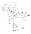
- FIG. 7 is a diagram of a common voltage generation circuit according to one embodiment of the present invention.
- FIG. 8 is a timing diagram of controlling a control signal corresponding to a first to a sixth switches in the common voltage generation circuit according to one embodiment of the present invention.
- FIGS. 9 ⁇ 13 are block diagrams depicting the display according to another embodiment of the present invention.
- FIG. 5 is a block diagram depicting a display 500 according to one embodiment of the present invention.
- the display 500 e.g. an LCD includes a display panel 501 e.g. an LCD panel, a gate driver 503 , and a source driver 505 .
- the display panel 501 includes a first pixel region 507 , a second pixel region 509 , and a common voltage generation circuit 511 .
- the first pixel region 507 has a plurality of first pixels (not shown) arranged in an i*j array for displaying images.
- i and j are positive integers.
- the second pixel region 509 has a plurality of second pixels 509 a disposed in the periphery of the first pixel region 507 .
- the common voltage generation circuit 511 is electrically connected to one of the second pixels 509 a in the second pixel region 509 , and the second pixel 509 a corresponds to one column of the pixels in the first pixel region 507 .
- the common voltage generation circuit 511 provides a common voltage V com to each of the first pixels in the first pixel region 507 based on a display voltage (V D ) of the drain of the TFT (not shown) in the second pixel 509 a electrically connected to the common voltage generation circuit 511 .
- V D display voltage
- the display voltage at a high voltage level V DH has positive polarity
- the display voltage at a low voltage level V DL has negative polarity.
- the common voltage V com is an average of the display voltages of positive and negative polarities. Namely, it can be expressed by the following equation.
- V com ( V DH +V DL )/2 Equation (4)
- the amount of the second pixel 509 a electrically connected to the common voltage generation circuit 511 is not limited in the present embodiment. However, it is required for said second pixel 509 a to be the one adjacent to the uppermost or the lowermost row in the first pixel region 507 . For example, if the display panel resolution of the present embodiment is i*j (e.g.
- the second pixel 509 a which is in the second pixel region 509 and is electrically connected to the common voltage generation circuit 511 is disposed in row 0 (in the second pixel region 509 adjacent to the first row of the pixels in the first pixel region 507 ) or in row 769 (in the second pixel region 509 adjacent to the 768 th row of the pixels in the first pixel region 507 ).
- the second pixel 509 a corresponding to the column of pixels in the first pixel region 507 is approximately positioned in the middle of the first pixel region 507 .
- the first pixel region 507 is an active pixel region
- the second pixel region 509 is a dummy pixel region.
- the gate driver 503 and the source driver 505 of the present embodiment respectively supply a scan voltage and a data voltage not only to each of the first pixels in the first pixel region 507 , but also to the row of pixels corresponding to the second pixel 509 a .
- the gate driver 503 and the source driver 505 are not the technical features of the present invention, and the principle of driving the gate driver 503 and the source driver 505 is well known to those skilled in the art. Hence, for fear of raising confusion between the related art and the present invention, detailed descriptions are then omitted.
- FIG. 6 illustrates a pixel configuration of a second pixel 509 a according to the present embodiment.
- FIG. 7 is a diagram of a common voltage generation circuit 511 according to the present embodiment. Please refer to FIGS. 5 ⁇ 7 together.
- the second pixel 509 a depicted in FIG. 6 adopts a Cs-on-common pixel configuration.
- the common voltage V com supplied to the first pixels and the second pixel 509 a is provided by the common voltage generation circuit 511 as is disclosed in FIG. 7 .
- the common voltage generation circuit 511 of the present embodiment includes operational amplifiers 701 , 703 , 705 , switches SW 1 ⁇ SW 6 , and capacitances C 1 ⁇ C 3 .
- operational amplifiers 701 and 703 disclosed in FIG. 7 .
- capacitances C 1 , C 2 and a peck detector consisting of the operational amplifier 705 and the capacitance C 3 are driven, respectively.
- each of the switches SW 1 ⁇ SW 6 has a control terminal which determines an ON/OFF state of the switches based on corresponding control signals C S1 ⁇ C S6 .
- the switches SW 1 , SW 2 , SW 5 are switched on while SW 3 , SW 4 , SW 6 are switched off.
- the switches SW 1 ⁇ SW 6 are switched off, and the node voltages V a , V b , and V c are in floating states.
- the switches SW 3 and SW 4 are switched on while SW 1 , SW 2 , SW 5 , SW 6 are switched off.
- the node voltage V a 0V
- V b is raised from 0V to [(V DH +V DL )/2]V in view of the principle of voltage division of the capacitances C 1 and C 2 .
- V c is raised from the negative high-pulsed display voltage ⁇ V DH to the positive low-pulsed display voltage V DL .
- the switches SW 4 and SW 6 are switched on while the switches SW 1 ⁇ 3 and SW 5 are switched off.
- the node voltage V b is supplied to the peak detector consisting of the operational amplifier 705 and the capacitance C 3 , so as to stabilize the voltage outputted to each of the first pixels in the first pixel region 507 .
- the outputted voltage is regarded as the common voltage V com required by each of the first pixels in the first pixel region 507 .
- the values of the input capacitances of the operational amplifiers 701 and 703 ought to be as small as possible.
- the values of the capacitances C 1 and C 2 must be identical and should be as large as possible. Thereby, the errors in the calculation of said common voltage V com can be eliminated.
- the common voltage generation circuit 511 of the present embodiment requires two frame times for calculating the outputted common voltage V com . It can also be learned from the timing of a scan signal GS.
- the common voltage generation circuit 511 memorizes the high-pulsed display voltage V DH
- the common voltage generation circuit 511 memorizes the low-pulsed display voltage V DL in the second frame time.
- the node voltage V b can be obtained and supplied to each of the first pixels in the first pixel region 507 as the common voltage V com required by each of the first pixels in the first pixel region 507 .
- the common voltage generation circuit 511 disclosed in the present embodiment From the operation of the common voltage generation circuit 511 disclosed in the present embodiment, it can be learned that the average of two voltage signals inputted at different frame times i.e. the average of the display voltages at the high voltage level V DH and at the low voltage level V DL is obtained. Therefore, the common voltage generation circuit 511 of the present embodiment can be applied to other technical fields in the event of obtaining the average voltage inputted at different frame times.
- the second pixel 509 a (the dummy pixel region) is adopted by the common voltage generation circuit 511 to calculate the common voltage V com required by the column of pixels in the display panel 501 .
- the gate driver 503 supplies the scan voltage to enable the row of pixels corresponding to the second pixel 509 a , and the data voltage supplied by the source driver 505 must be driven in the manner as driving the display panel 501 i.e. a normally white manner or a normally black manner.
- the correct data voltage (white signal or black signal) is correspondingly supplied to the column of pixels, and the gray level of the supplied data voltage must be consistent.
- the data voltage which is supplied to the column of the pixels corresponding to the second pixel 509 a by the source driver 505 must be a white signal.
- the data voltage which is supplied to the column of the pixels corresponding to the second pixel 509 a by the source driver 505 must be a black signal.
- the state of the scan voltage outputted by the gate driver 503 and that of the data voltage outputted by the source driver 505 ought to be taken into consideration even though the row of pixels corresponding to the second pixel 509 a is not used at the time the display panel 501 is driven.
- the column of pixels corresponding to the second pixel 509 a is capable of resolving the problem of the feed-through voltage ( ⁇ V D ) of the scan voltage in the display panel, and further eliminating the flicker noises of the display panel 501 thoroughly.
- said problem of the feed-through voltage ( ⁇ V D ) of the scan voltage results from the RC delay induced by the parasitic capacitance and the parasitic resistance on the scan line.
- the RC delay on the scan line poses less impact on the first pixels adjacent to the column of pixels corresponding to the second pixel 509 a and is disposed in the display panel 501 .
- the first pixels far from the middle of the display panel 501 are still likely to be affected by the RC delay on the scan line.
- the flicker noises may occur in the first pixels at two sides of the display panel 501 .
- the flicker noises occurring in the first pixels at two sides of the display panel 501 the flicker noises occurring in the first pixels adjacent to the display panel 501 or corresponding to the second pixel 509 a can be reduced.
- the common voltage V com supplied to each of the first pixels in the display panel 501 is automatically generated by the common voltage generation circuit 511 rather than supplied outside. Thereby, the voltage across the liquid crystal capacitance C LC and the storage capacitance C S remains consistent, and the gray level accuracy of each of the first pixels in the first pixel region 507 is further improved. Accordingly, the complicated process of conventional manual adjustment of the common voltage V com can be eliminated, and the best common voltage V com required by the first pixels in the display panel 501 can be obtained.
- Said embodiment has taken one second pixel 509 a in the second pixel region 509 electrically connected to the common voltage generation circuit 511 for an example.
- another embodiment taking a plurality of the second pixels 509 a in the second pixel region 509 electrically connected to the common voltage generation circuit 511 for an example is provided hereinafter.
- FIG. 9 is a block diagram depicting a display 900 according to another embodiment of the present invention. Please refer to FIGS. 5 and 9 together.
- the difference between the display 900 of FIG. 9 and the display 500 lies in that the common voltage generation circuit 511 is electrically connected to four of the second pixels 509 a in the second pixel region 509 .
- two of the second pixels 509 a are disposed adjacent to the uppermost row of the pixels in the first pixel region 507
- the other two of the second pixels 509 a are disposed adjacent to the lowermost row of the pixels in the first pixel region 507 .
- the disposition represented in FIG. 9 but not limited in the present embodiment can be adjusted according to the design of the display panel 501 .
- the common voltage generation circuit 511 of the present embodiment is electrically connected to four of the second pixels 509 a in the second pixel region 509 . Hence, it can be anticipated that the flicker noises of the display panel 501 are significantly reduced, and the display quality of the display 900 is improved.
- FIG. 10 is a block diagram depicting a display 1000 according to another embodiment of the present invention. Please refer to FIG. 10 .
- the common voltage generation circuit 511 is electrically connected to ten of the second pixels 509 a in the second pixel region 509 .
- five of the second pixels 509 a are disposed adjacent to the uppermost row of the pixels in the first pixel region 507
- the other five of the second pixels 509 a are disposed adjacent to the lowermost row of the pixels in the first pixel region 507 .
- the disposition represented in FIG. 10 but not limited in the present embodiment can be adjusted according to the design of the display panel 501 .
- the common voltage generation circuit 511 of the present embodiment is electrically connected to ten of the second pixels 509 a in the second pixel region 509 . Hence, it can be anticipated that the flicker noises of the display panel 501 are further reduced to a great extent, and the display quality of the display 1000 is better than that of the displays 500 and 900 .
- the common voltage generation circuit 511 when the common voltage generation circuit 511 is electrically connected to more of the second pixels 509 a in the second pixel region 509 , the problem of the drift of the feed-through voltage ( ⁇ V D ) caused by the RC delay of the parasitic-capacitance and the parasitic-resistance on the scan line can be avoided when said embodiment is applied to an actual display panel. Further, the flicker noises of the display panel 501 can be reduced, thus significantly promoting the display quality.
- a photo mask is adopted to divide a color filter of the display panel into a plurality of areas, and the common voltage generation circuit 511 described above is employed to supply the common voltage required by the pixels in each of the areas.
- the three embodiments also have advantages similar to those of the former embodiments.
- FIG. 11 is a block diagram depicting a display 1100 according to another embodiment of the present invention. Please refer to FIG. 11 .
- the display 1100 adopts a photo mask to divide a color filter (not shown) into three areas. That is, the display panel 501 is divided into three areas: area A, area B, and area C.
- the areas A, B, and C have corresponding second pixel 509 a respectively and a common voltage V com provided by the common voltage generation circuit 511 .
- the principle of operating the display 1100 is similar to that of operating the display 500 described in the former embodiments, further descriptions are omitted.
- FIGS. 12 and 13 are block diagrams depicting displays 1200 and 1300 according to another embodiment of the present invention. Please refer to FIGS. 11 ⁇ 13 together.
- the displays 1200 and 1300 are similar to the display 1100 .
- the difference lies in that the display 1200 adopts a photo mask to divide a color filter into five areas, while the display 1300 divides the color filter into ten areas.
- the display panel of the display 1200 is divided into five areas A ⁇ E, and that of the display 1300 is divided into ten areas A ⁇ J.
- the common voltage generation circuit 511 described above is employed to supply the common voltage required in each of the areas. Thereby, the flicker noises of the display panel can be completely avoided, thus promoting the display quality.
- the present invention provides a display and a display panel thereof. According to the spirit of the present invention, the present invention has the following advantages:
- the common voltage generation circuit Through the electrical connection of the common voltage generation circuit to at least a second pixel in the second pixel region, and through the automatic adjustment of the common voltage of the pixel corresponding to one column of pixels in the display panel in N frame time (N is a positive integer, e.g. 2), the complicated process of conventional manual adjustment of the common voltage can be eliminated. Furthermore, the common voltage provided by the common voltage generation circuit is ensured to be at the best voltage level required by the column of the pixels in the display panel.
- the color filter is divided into a plurality of areas, and so is the display panel.
Abstract
Description
V com=(V DH +V DL)/2 Equation (4)
Claims (20)
Applications Claiming Priority (3)
| Application Number | Priority Date | Filing Date | Title |
|---|---|---|---|
| TW95142533 | 2006-11-17 | ||
| TW95142533A | 2006-11-17 | ||
| TW095142533A TWI354968B (en) | 2006-11-17 | 2006-11-17 | Liquid crystal display and display panel thereof |
Publications (2)
| Publication Number | Publication Date |
|---|---|
| US20080117148A1 US20080117148A1 (en) | 2008-05-22 |
| US8089435B2 true US8089435B2 (en) | 2012-01-03 |
Family
ID=39416441
Family Applications (1)
| Application Number | Title | Priority Date | Filing Date |
|---|---|---|---|
| US11/691,505 Expired - Fee Related US8089435B2 (en) | 2006-11-17 | 2007-03-27 | Liquid crystal display and display panel thereof |
Country Status (2)
| Country | Link |
|---|---|
| US (1) | US8089435B2 (en) |
| TW (1) | TWI354968B (en) |
Cited By (2)
| Publication number | Priority date | Publication date | Assignee | Title |
|---|---|---|---|---|
| US20100245326A1 (en) * | 2009-03-25 | 2010-09-30 | Beijing Boe Optoelectronics Technology Co., Ltd. | Common electrode drive circuit and liquid crystal display |
| TWI682632B (en) * | 2014-12-26 | 2020-01-11 | 日商半導體能源研究所股份有限公司 | Semiconductor device |
Families Citing this family (15)
| Publication number | Priority date | Publication date | Assignee | Title |
|---|---|---|---|---|
| KR101256665B1 (en) * | 2005-12-30 | 2013-04-19 | 엘지디스플레이 주식회사 | Liquid crystal panel |
| TWI339378B (en) * | 2007-05-11 | 2011-03-21 | Chimei Innolux Corp | Liquid crystal display device and method for driving the same |
| JP2009294499A (en) * | 2008-06-06 | 2009-12-17 | Oki Semiconductor Co Ltd | Liquid crystal display device and liquid crystal display controller |
| TWI413052B (en) * | 2009-10-02 | 2013-10-21 | Innolux Corp | Pixel array and driving method thereof and display panel employing the pixel array |
| CN102426827A (en) * | 2011-12-14 | 2012-04-25 | 南京中电熊猫液晶显示科技有限公司 | Data output method of time sequence controller |
| KR101396688B1 (en) * | 2012-05-25 | 2014-05-19 | 엘지디스플레이 주식회사 | Liquid crystal display device and driving method thereof |
| CN103295540B (en) * | 2012-06-07 | 2015-06-10 | 上海天马微电子有限公司 | Driving method, driving device and display for active matrix display panel |
| KR102315963B1 (en) * | 2014-09-05 | 2021-10-22 | 엘지디스플레이 주식회사 | Display Device |
| TWI550591B (en) * | 2015-06-04 | 2016-09-21 | 友達光電股份有限公司 | Display device and method thereof |
| US10380937B2 (en) * | 2015-08-26 | 2019-08-13 | Apple Inc. | Multi-zoned variable VCOM control |
| JP2017198914A (en) * | 2016-04-28 | 2017-11-02 | Tianma Japan株式会社 | Display device |
| JP2018155964A (en) * | 2017-03-17 | 2018-10-04 | 株式会社ジャパンディスプレイ | Display and method for adjusting common voltage of display |
| CN107123408B (en) * | 2017-06-22 | 2019-08-30 | 深圳市华星光电技术有限公司 | Public voltage generating circuit and liquid crystal display |
| CN108172185A (en) * | 2018-01-03 | 2018-06-15 | 深圳禾苗通信科技有限公司 | It is a kind of to reduce the uneven method of LCD panel flicker flickers |
| CN109215610B (en) * | 2018-11-13 | 2020-05-12 | 惠科股份有限公司 | Method, device and system for determining actual optimal common voltage of display panel |
Citations (3)
| Publication number | Priority date | Publication date | Assignee | Title |
|---|---|---|---|---|
| US6392626B1 (en) | 1998-11-06 | 2002-05-21 | Samsung Electronics Co., Ltd. | Liquid crystal display having different common voltages |
| CN1527271A (en) | 2003-03-03 | 2004-09-08 | ��ʽ����������ʾ�� | Image display device |
| US20070115241A1 (en) * | 2005-11-21 | 2007-05-24 | Kentaro Teranishi | Display panel control circuit and display device |
-
2006
- 2006-11-17 TW TW095142533A patent/TWI354968B/en not_active IP Right Cessation
-
2007
- 2007-03-27 US US11/691,505 patent/US8089435B2/en not_active Expired - Fee Related
Patent Citations (4)
| Publication number | Priority date | Publication date | Assignee | Title |
|---|---|---|---|---|
| US6392626B1 (en) | 1998-11-06 | 2002-05-21 | Samsung Electronics Co., Ltd. | Liquid crystal display having different common voltages |
| CN1527271A (en) | 2003-03-03 | 2004-09-08 | ��ʽ����������ʾ�� | Image display device |
| US20040239667A1 (en) * | 2003-03-03 | 2004-12-02 | Hiroyuki Takahashi | Image display device |
| US20070115241A1 (en) * | 2005-11-21 | 2007-05-24 | Kentaro Teranishi | Display panel control circuit and display device |
Cited By (3)
| Publication number | Priority date | Publication date | Assignee | Title |
|---|---|---|---|---|
| US20100245326A1 (en) * | 2009-03-25 | 2010-09-30 | Beijing Boe Optoelectronics Technology Co., Ltd. | Common electrode drive circuit and liquid crystal display |
| US8878829B2 (en) * | 2009-03-25 | 2014-11-04 | Beijing Boe Optoelectronics Technology Co., Ltd. | Liquid crystal display and common electrode drive circuit thereof |
| TWI682632B (en) * | 2014-12-26 | 2020-01-11 | 日商半導體能源研究所股份有限公司 | Semiconductor device |
Also Published As
| Publication number | Publication date |
|---|---|
| TWI354968B (en) | 2011-12-21 |
| US20080117148A1 (en) | 2008-05-22 |
| TW200823824A (en) | 2008-06-01 |
Similar Documents
| Publication | Publication Date | Title |
|---|---|---|
| US8089435B2 (en) | Liquid crystal display and display panel thereof | |
| US6166714A (en) | Displaying device | |
| US7916108B2 (en) | Liquid crystal display panel with color washout improvement and applications of same | |
| KR100377600B1 (en) | Method for driving a liquid crystal display | |
| US6222516B1 (en) | Active matrix liquid crystal display and method of driving the same | |
| US8325126B2 (en) | Liquid crystal display with reduced image flicker and driving method thereof | |
| KR101318043B1 (en) | Liquid Crystal Display And Driving Method Thereof | |
| US7812896B2 (en) | Liquid crystal display and driving method thereof | |
| US8085230B2 (en) | Driving device and display apparatus having the same | |
| KR100385106B1 (en) | Source driver, source line drive circuit, and liquid crystal display device using the same | |
| US20050259092A1 (en) | Image-correction-amount detecting device, circuit for driving electro-optical device, electro-optical device, and electronic apparatus | |
| US8248343B2 (en) | Liquid crystal display panel and method for driving pixels thereof | |
| US20080024417A1 (en) | Common voltage compensation device, liquid crystal display, and driving method thereof | |
| US20080259234A1 (en) | Liquid crystal display device and method for driving same | |
| US8451262B2 (en) | Method of driving a display panel, and display apparatus for performing the method | |
| US9230497B2 (en) | Display device having each pixel divided into sub pixels for improved view angle characteristic | |
| US8982287B2 (en) | Data processing apparatus, liquid crystal display device, television receiver, and data processing method | |
| CN114038438B (en) | Drive circuit and display device | |
| US8068085B2 (en) | Electro-optical device, method of driving electro-optical device, and electronic apparatus | |
| US7948595B2 (en) | Liquid crystal display panel | |
| US6911966B2 (en) | Matrix display device | |
| KR101585688B1 (en) | Liquid Crystal Display and Driving Method thereof | |
| KR101461018B1 (en) | Liquid crystal display device and driving method of the same | |
| CN113870806A (en) | Compensation system and method for dual gate display | |
| KR20070077350A (en) | Liquid crystal display device |
Legal Events
| Date | Code | Title | Description |
|---|---|---|---|
| AS | Assignment |
Owner name: CHUNGHWA PICTURE TUBES, LTD., TAIWAN Free format text: ASSIGNMENT OF ASSIGNORS INTEREST;ASSIGNOR:TU, CHANG-CHING;REEL/FRAME:019185/0368 Effective date: 20070323 |
|
| ZAAA | Notice of allowance and fees due |
Free format text: ORIGINAL CODE: NOA |
|
| ZAAB | Notice of allowance mailed |
Free format text: ORIGINAL CODE: MN/=. |
|
| STCF | Information on status: patent grant |
Free format text: PATENTED CASE |
|
| FPAY | Fee payment |
Year of fee payment: 4 |
|
| MAFP | Maintenance fee payment |
Free format text: PAYMENT OF MAINTENANCE FEE, 8TH YEAR, LARGE ENTITY (ORIGINAL EVENT CODE: M1552); ENTITY STATUS OF PATENT OWNER: LARGE ENTITY Year of fee payment: 8 |
|
| FEPP | Fee payment procedure |
Free format text: MAINTENANCE FEE REMINDER MAILED (ORIGINAL EVENT CODE: REM.); ENTITY STATUS OF PATENT OWNER: LARGE ENTITY |
|
| LAPS | Lapse for failure to pay maintenance fees |
Free format text: PATENT EXPIRED FOR FAILURE TO PAY MAINTENANCE FEES (ORIGINAL EVENT CODE: EXP.); ENTITY STATUS OF PATENT OWNER: LARGE ENTITY |
|
| STCH | Information on status: patent discontinuation |
Free format text: PATENT EXPIRED DUE TO NONPAYMENT OF MAINTENANCE FEES UNDER 37 CFR 1.362 |
|
| FP | Lapsed due to failure to pay maintenance fee |
Effective date: 20240103 |