US8089274B2 - Method for evaluating SOI wafer - Google Patents
Method for evaluating SOI wafer Download PDFInfo
- Publication number
- US8089274B2 US8089274B2 US12/227,687 US22768707A US8089274B2 US 8089274 B2 US8089274 B2 US 8089274B2 US 22768707 A US22768707 A US 22768707A US 8089274 B2 US8089274 B2 US 8089274B2
- Authority
- US
- United States
- Prior art keywords
- soi
- layer
- sheet resistance
- soi wafer
- wafer
- Prior art date
- Legal status (The legal status is an assumption and is not a legal conclusion. Google has not performed a legal analysis and makes no representation as to the accuracy of the status listed.)
- Active, expires
Links
Images


Classifications
-
- H—ELECTRICITY
- H10—SEMICONDUCTOR DEVICES; ELECTRIC SOLID-STATE DEVICES NOT OTHERWISE PROVIDED FOR
- H10D—INORGANIC ELECTRIC SEMICONDUCTOR DEVICES
- H10D86/00—Integrated devices formed in or on insulating or conducting substrates, e.g. formed in silicon-on-insulator [SOI] substrates or on stainless steel or glass substrates
-
- H—ELECTRICITY
- H10—SEMICONDUCTOR DEVICES; ELECTRIC SOLID-STATE DEVICES NOT OTHERWISE PROVIDED FOR
- H10P—GENERIC PROCESSES OR APPARATUS FOR THE MANUFACTURE OR TREATMENT OF DEVICES COVERED BY CLASS H10
- H10P74/00—Testing or measuring during manufacture or treatment of wafers, substrates or devices
- H10P74/20—Testing or measuring during manufacture or treatment of wafers, substrates or devices characterised by the properties tested or measured, e.g. structural or electrical properties
- H10P74/207—Electrical properties, e.g. testing or measuring of resistance, deep levels or capacitance-voltage characteristics
-
- H—ELECTRICITY
- H10—SEMICONDUCTOR DEVICES; ELECTRIC SOLID-STATE DEVICES NOT OTHERWISE PROVIDED FOR
- H10P—GENERIC PROCESSES OR APPARATUS FOR THE MANUFACTURE OR TREATMENT OF DEVICES COVERED BY CLASS H10
- H10P74/00—Testing or measuring during manufacture or treatment of wafers, substrates or devices
Definitions
- the present invention relates to a method for evaluating a SOI wafer, and particularly relates to a method for evaluating a SOI wafer, in which characteristics of a buried diffusion layer are evaluated in the SOI wafer having the buried diffusion layer.
- a silicon substrate which is generally used as a semiconductor substrate used in an integrated circuit
- a semiconductor device with high speed and low power consumption is further required with improvement in speed and high integration of a system or development of a mobile terminal in recent years.
- an SOI wafer having a SOI (Silicon On Insulator) structure in which a silicon active layer (SOI layer) is formed on an insulated layer can meet operation of devices with higher speed and low power consumption, and if the SOI wafer is used, device fabrication can be made without a significant change in established equipment, processes, or the like of device processes for a bulk wafer which does not have the SOI structure, so that the SOI wafer has been attracting attention as a wafer that can realize the operation of the devices with higher speed and low power consumption.
- SOI Silicon On Insulator
- FIG. 4 A general structure of such an SOI wafer is shown in FIG. 4 .
- a SOI layer 15 is formed on a supporting substrate 13 composed of silicon single crystal or the like so as to dispose a buried insulated layer 14 therebetween.
- a buried diffusion layer 12 in which impurities are diffused in high concentration is formed in an interface region in the SOI layer 15 with the insulated layer 14 in some cases as shown in FIG. 4 .
- the SOI layer 15 has the buried diffusion layer 12 and a low concentration layer 11 whose impurity concentration is lower than that in the buried diffusion layer.
- the SOI wafer has been attracting a lot of attention as described above and accurate evaluation of characteristics of the SOI wafer has been required, so that various researches on the evaluation method have been currently conducted.
- evaluation of the characteristics on a surface of the SOI layer can be performed by contacting an electrode and a probe on front and back surfaces of the SOI wafer for measurement as disclosed in, for example, Japanese Unexamined Patent Publication (Kokai) No. 2000-277716, without using a four-point probe method.
- the buried diffusion layer 12 is buried in the SOI wafer, so that evaluation of characteristics of the layer has been difficult.
- a wafer to be the monitor wafer is prepared (a).
- an oxide film is formed on the front surface of the base wafer (Box oxidization) (b).
- screen oxidization of the surface (c) and impurity ion implantation (d) are simultaneously performed on both the bond wafer to be the active layer of the SOI wafer to be the product and the monitor wafer.
- a screen oxide film is then removed (e), and the base wafer and the bond wafer are cleaned and subsequently subjected to bonding heat treatment (g), for example, under an oxygen atmosphere through a bonding process (f).
- thinning the bond wafer is then performed by, for example, grinding and polishing (h), and are further polished and cleaned (i) to fabricate the product SOI wafer (l).
- the monitor wafer it is subjected to heat treatment under a nitrogen atmosphere (g) separately from the SOI wafer to be the product and subsequently a screen oxide film is removed (j).
- the evaluation of the buried diffusion layer of the SOI wafer to be the product has been performed indirectly by measuring sheet resistance of a high-impurity concentration diffusion layer thus formed on the monitor wafer (k).
- the present invention is made in view of such problems, and an object thereof is to provide a method for evaluating the SOI wafer that can directly measure the SOI wafer itself to be the product to thereby evaluate the sheet resistance of the buried diffusion layer thereof, without fabricating the monitor wafer.
- the present invention is made to solve the above described problems, and an object thereof is to provide a method for evaluating an SOI wafer characterized in that in a method for evaluating an SOI wafer in which a sheet resistance of a buried diffusion layer of an SOI wafer that has at least an SOI layer on an insulator layer and has a buried diffusion layer whose impurity concentration is higher than other region of the SOI layer in an interface area with the insulator layer of the SOI layer, the method including the steps of measuring a sheet resistance of the whole SOI layer or the whole SOI wafer, and estimating the sheet resistance of the buried diffusion layer by assuming respective layers that compose the SOI wafer to be resistors connected in parallel and converting the measured result of the sheet resistance measurement.
- the sheet resistance of the buried diffusion layer of the SOI wafer having the buried diffusion layer when the sheet resistance of the whole SOI layer or the whole SOI wafer is measure, and the sheet resistance of the buried diffusion layer is estimated by assuming and converting the measured results of the sheet resistance as the resistance of respective layers that compose the SOI wafer being connected in parallel, the sheet resistance of the buried diffusion layer of the SOI wafer to be a product can be directly evaluated nondestructively. For this reason, the buried diffusion layers of all the manufactured SOI wafers can also be inspected, thus allowing quality of the SOI wafers to be assured. Moreover, since the monitor wafer is not needed, a material cost and the number of processes for fabricating the monitor wafer can be reduced.
- measuring the sheet resistance of the whole SOI wafer can include the steps of radiating lines of magnetic force of an alternating current magnetic field to one surface of the SOI wafer to form eddy currents caused by the alternating current magnetic field on the SOI wafer, measuring variation of the magnetic field according to eddy current loss generated by the eddy current formation, on a surface opposite to the surface to which the lines of magnetic force are radiated, and calculating the sheet resistance of the whole SOI wafer from the measured variation of the magnetic field.
- the sheet resistance of the whole SOI wafer is measured by the method for measuring the variation of the magnetic field caused by the eddy currents
- the sheet resistance of the buried diffusion layer of the SOI wafer can be evaluated without contacting the SOI wafer with a measuring instrument.
- the SOI wafer can be evaluated without contacting the SOI wafer, there is no need to clean the wafer after the evaluation.
- measuring the sheet resistance of the whole SOI layer can be performed by applying a four-point probe method to a surface of the whole SOI layer.
- the sheet resistance of the buried diffusion layer of the SOI wafer can be evaluated by a simpler measuring instrument.
- the probes shall be contacted with the surface of the SOI layer, there is no problem if cleaning or polishing is performed after the evaluation.
- the sheet resistance of the buried diffusion layer of the SOI wafer to be the product can be directly evaluated without fabricating the monitor wafer.
- a material cost or a cost of the number of processes or the like for fabricating the monitor wafer can be reduced.
- all the product SOI wafers can also be tested, and thus the quality thereof can be fully assured.
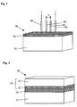
- FIG. 1 is a schematic view showing an aspect of measuring resistivity of a whole SOI wafer by an eddy current method according to the present invention
- FIG. 2 is a schematic view showing an aspect of measuring resistivity of a whole SOI layer with a four-point probe method according to the present invention
- FIG. 3 is a schematic view showing an aspect of measuring sheet resistance of a high concentration diffusion layer of a monitor wafer
- FIG. 4 is a schematic view showing an SOI wafer having a general buried diffusion layer
- FIG. 5 is a flow chart showing a method for evaluating a buried diffusion layer of a product SOI wafer without fabricating the monitor wafer according to the present invention
- FIG. 6 is a flow chart showing a conventional method for fabricating the monitor wafer to evaluate the buried diffusion layer of the product SOI wafer;
- FIG. 7 is a graph plotting a curve showing a relation between resistivity of a supporting substrate and that of the whole SOI wafer calculated by an approximate equation (4), and a curve showing resistivity of the whole SOI wafer measured in an experimental example;
- FIG. 8 is a graph plotting a curve showing a relation between sheet resistance of the buried diffusion layer and that of the whole SOI wafer calculated with approximate equation (4), and a curve showing resistivity of the whole SOI wafer measured in the experimental example;
- FIG. 9 is a graph showing a correlation between the sheet resistance of the buried diffusion layer evaluated with a method for evaluating the buried diffusion layer according to the eddy current method of the present invention and the sheet resistance of the high concentration diffusion layer measured on the monitor wafer;
- FIG. 10 is a graph showing a correlation between the sheet resistance of the buried diffusion layer evaluated with a method for evaluating the buried diffusion layer according to the four-point probe method of the present invention and the sheet resistance of the high concentration diffusion layer measured on the monitor wafer.
- a monitor wafer method As described above, according to the conventional method for fabricating a monitor wafer separately from an SOI wafer to be a product to measure sheet resistance of a front surface of the monitor wafer in which a high concentration diffusion layer (buried diffusion layer) is exposed (hereinafter, it may be referred to as a monitor wafer method), there have been problems that a cost for fabricating the monitor wafer is required in addition to a cost for manufacturing the product SOI wafer and the product SOI wafer cannot be evaluated directly.
- a cost for fabricating the monitor wafer is required in addition to a cost for manufacturing the product SOI wafer and the product SOI wafer cannot be evaluated directly.
- the inventor has found out that as for the product SOI wafer, sheet resistance of a whole SOI wafer or a whole SOI layer is measured, and the sheet resistance of the buried diffusion layer of the product SOI wafer can be estimated by considering and converting the measured results as a resistance of each layers composing the SOI wafer being connected in parallel respectively, and completed the present invention.
- FIG. 5 An example of a method for evaluating the sheet resistance of the buried diffusion layer of the SOI wafer according to the present invention is schematically shown in FIG. 5 .
- Steps (a) to (i) in FIG. 5 show processes for manufacturing the SOI wafer, which has the SOI layer on the insulated layer and has the buried diffusion layer in an interface area in the SOI layer with the insulated layer, according to the usual method.
- the SOI wafer can be manufactured in a same way as with a conventional method for manufacturing the product SOI wafer in FIG. 6 .
- the SOI wafer fabricated in this way is then subjected to sheet resistance measurement at step (j) with the method for evaluating the SOI wafer according to the present invention.
- the method for manufacturing the SOI wafer is not limited to the above-described (a) to (i) in FIG. 5 , but the SOI wafer may be manufactured with any manufacturing method as long as it is the method for manufacturing the SOI wafer having the buried diffusion layer.
- the SOI wafer is cleaned as needed (k) to make the product SOI wafer (l). A specific method of the sheet resistance measurement at step (j) which is an essential part of the present invention will be described later.
- the SOI wafer manufactured in this way is the conventional SOI wafer having the buried diffusion layer as shown in FIG. 4 .
- FIG. 4 shows an SOI wafer 10 in which a supporting substrate 13 , a buried insulated layer 14 , and a SOI layer 15 composed of a buried diffusion layer 12 and a low impurity concentration layer 11 whose concentration is lower than that of the buried diffusion layer are stacked
- the structure of the SOI wafer to which the present invention is applied is not limited to this.
- it may be an SOI wafer in which a silicon layer is directly formed on an insulator substrate.
- the buried insulated layer is not limited to the silicon oxide film, but the insulated layer may be a nitride film or the like.
- One of embodiments according to the present invention is a method for measuring the sheet resistance of the whole SOI wafer and estimating the sheet resistance of the buried diffusion layer from the measured results by an eddy current method as described below.
- an alternating current magnetic field B 1 is radiated to one surface of the SOI wafer 10 (in FIG. 1 , it is a front surface of the SOI layer 15 ).
- an alternating current can be made to flow through a magnetic field radiation head 31 having a coil 32 as shown in FIG. 1 , for example, and according to such a method, the alternating current magnetic field can be radiated using an apparatus with a simple structure.
- the alternating current magnetic field B 1 thus radiated penetrates through each layer of the SOI wafer 10 , namely, the low concentration layer 11 , the buried diffusion layer 12 , the buried insulated layer 14 , and the supporting substrate 13 . Since the radiated magnetic field is the alternating current, the magnetic field in each layer of the SOI wafer 10 changes, and eddy currents are generated around a magnetic flux in each layer by an electromagnetic induction action so as to counteract the change in the magnetic field. However, since the buried insulated layer 14 is an insulator, the eddy currents to be generated are small enough to be ignored.
- the eddy currents thus generated on each layer of the SOI wafer 10 causes energy loss (eddy current loss) by Joule heat.
- the eddy current loss can also be ignored.
- the alternating current magnetic field B 1 radiated on the SOI wafer 10 penetrates through the whole SOI wafer, and then changes according to the above-described eddy current loss into a magnetic field B 2 on a surface opposite to the radiated one.
- a measuring head 41 having a coil 42 may be used, for example. Due to a change with the passage of time in the magnetic field B 2 , currents flow through the coil 42 by electromagnetic induction. A tester or the like which is not shown is connected to the measuring head 41 , and resistivity ⁇ of the whole SOI wafer 10 is measured.
- the sheet resistance of the buried diffusion layer 12 can be calculated from this resistivity ⁇ of the whole SOI wafer 10 as henceforth described.
- the sheet resistances of the low concentration layer 11 , the buried diffusion layer 12 , and the supporting substrate 13 be R 1 , R 2 , and R 3 , respectively
- the sheet resistance R of the whole SOI wafer can be represented by Equation (2).
- the buried insulated layer 14 is the insulator, influence due to the resistance of the buried insulated layer 14 can be ignored.
- Equation (3) Equation (3) is obtained.
- Equation (2) can be approximated as Equation (4).
- Equation (4) the sheet resistance R 3 of the supporting substrate 13 is already known as described above.
- a relation between the sheet resistance R 2 of the buried diffusion layer 12 and the resistivity ⁇ of the whole SOI wafer 10 is calculated from approximate equation (4) and is shown in FIG. 8 .
- curves (a), (b), and (c) show the relations when the resistivity ⁇ 3 of the supporting substrate 13 is 2.4 ⁇ cm and the thickness t 3 are 725 ⁇ m, 625 ⁇ m, and 450 ⁇ m, respectively.
- Equation (4) when Equation (4) is transformed about the sheet resistance R 2 of the buried diffusion layer 12 , it is represented as Equation (5).
- the sheet resistance R 3 obtained from the resistivity ⁇ 3 and the thickness t 3 of the supporting substrate 13 is already known as described above, the sheet resistance R 2 of the buried diffusion layer 12 can be obtained from the whole resistance R of the SOI wafer 10 measured as described above.
- the sheet resistance R 2 of the buried diffusion layer can be calculated by measuring the whole resistance R of the SOI wafer 10 as the variation of the magnetic field and converting the whole resistance R according to approximate equation (5).
- the SOI wafer 10 having the buried diffusion layer 12 as shown in FIG. 4 , and a monitor wafer 70 corresponding thereto as shown in FIG. 3 namely, a monitor wafer having a high concentration diffusion layer 72 formed on a front surface area of a silicon wafer 71 were fabricated.
- the base wafer to be the supporting substrate 13 was used in which the conductive type is p-type, the resistivity is 10 ⁇ cm, and the thickness is 725 ⁇ m, and the dose amount of arsenic to be ion-implanted was set to 1 ⁇ 10 15 atoms/cm 2 , and the film thickness t 2 of the buried diffusion layer 12 was 2 ⁇ m.
- the product SOI wafer manufactured in this way was subjected to sheet resistance measurement of the buried diffusion layer 12 by the eddy current method of the present invention, and the resistivity ⁇ 2 of the buried diffusion layer 12 was obtained. The results were shown as a point (e) in FIG. 7 .
- a sheet resistance R s of the high concentration diffusion layer 72 was measured by measuring the sheet resistance of the surface of the high concentration diffusion layer 72 as the measuring surface, using the four-point probe method in which current probes 62 and voltage probes 63 and 63 were pressed to the surface.
- the sheet resistance was about 70 ⁇ / ⁇ .
- the product SOI wafer and the monitor wafer were fabricated in a manner similar to that of the first experimental example except for ion-implanting the dose amount of arsenic of 2 ⁇ 10 15 atoms/cm 2 into a p-type silicon wafer with a resistivity of 2.4 ⁇ cm, and the sheet resistance R 2 of the buried diffusion layer was evaluated. The results were shown as a point (f) in FIG. 7 .
- the sheet resistance R s of the high concentration diffusion layer 72 was measured by the four-point probe method in a manner similar to that of the first experimental example.
- the sheet resistance of the monitor wafer was about 35 ⁇ / ⁇ .
- the results were shown as a point (d) in FIG. 8 .
- the sheet resistance of the buried diffusion layer can be calculated approximate equation (5).
- Equation (2) is better approximated to approximate equation (4), namely, the larger R 1 is and the larger the difference from R 2 and R 3 is, the more correctly the R 2 can be estimated.
- the sheet resistance of the whole SOI wafer 10 can be preferably measured with less error.
- the sheet resistance of the buried diffusion layer of the product SOI wafer can be directly evaluated. Note herein that, since measuring the sheet resistance of the whole SOI wafer 10 by this eddy current method can be performed without contacting with a measuring instrument, there is no fear of generating dust or the like, and a cleaning process (step (k) in FIG. 5 ) after the measurement can also be omitted.
- Another embodiment of the present invention is a method for measuring the sheet resistance of the whole SOI layer by applying the four-point probe method on the surface of the SOI layer to thereby estimate the sheet resistance of the buried diffusion layer from the measured results.
- the current probes 62 and 62 and the voltage probes 63 and 63 are pressed to the surface of the SOI layer 15 of the SOI wafer 10 to measure a sheet resistance R SOI of the whole SOI layer 15 by the four-point probe method.
- the four-point probe method is a technique for measuring the sheet resistance of that sample in such a way that total four probes of the current probes 62 and 62 and the voltage probes 63 and 63 are pressed to a sample surface (here, the surface of the SOI layer 15 ) while arranging them linearly and at almost equal intervals, and a current I is made to flow between the current probes 62 and 62 to thereby measure a voltage between the voltage probes 63 and 63 .
- the sheet resistance of the whole SOI layer 15 including the buried diffusion layer 12 can be measured. Namely, when the SOI layer is junction-separated by a diode structure or the like, for example, when a conductivity type of the buried diffusion layer 12 is p-type and a conductivity type of the low concentration layer 11 is n-type, the sheet resistance of the whole SOI layer 15 cannot be measured from the surface of the SOI layer 15 by the four-point probe method, so that the present embodiment cannot be applied.
- the supporting substrate 13 is insulated from the SOI layer 15 by the buried insulated layer 14 in this method, the supporting substrate 13 does not have an influence on the measurement.
- Equation (6) The following calculation is performed by assuming that respective layers of the SOI layer 15 , namely, the low concentration layer 11 and the buried diffusion layer 12 are resistances connected in parallel. By this assumption, Equation (6) is obtained.
- Equation (7) is obtained.
- Equation 8 R SOI ⁇ R 2 (8)
- Equation (7) is better approximated to approximate equation (8), namely, the larger the difference between R 1 and R 2 is, the more correctly the R 2 can be preferably estimated.
- the difference is large enough if the R 2 is not more than 100 ⁇ / ⁇ when the R 1 is not less than 1 k ⁇ / ⁇ .
- the four-point probe method since there is a possibility that the probes contact to the surface of the SOI layer to generate contamination, such as dust or the like on the front surface of the SOI wafer, it is preferable to clean or polish, after measuring the sheet resistance R SOI , the SOI wafer before determining it as the product SOI wafer ( FIG. 5 ( k )).
- the SOI wafer is determined as the product SOI wafer ( FIG. 5 ( l )).
- the sheet resistance of the buried diffusion layer can be directly evaluated without fabricating the monitor wafer and with the simple method.
- one monitor wafer for each SOI wafer namely, five monitor wafers in total were fabricated according to fabricating processes of the monitor wafer shown in FIG. 6 simultaneously with manufacturing the SOI wafers.
- the sheet resistance R 2 of the buried diffusion layers was obtained by calculation (Example 1).
- Example 1 As in Example 1, according to the processes (a) to (i) shown in FIG. 5 , ten sheets of SOI wafers having the buried diffusion layers were manufactured by the usual method. An accelerating voltage was set to 100 keV in the ion implantation of arsenic, and dose amount was fine-tuned to change in the range of 2 ⁇ 10 15 atoms/cm 2 to 4 ⁇ 10 15 atoms/cm 2 .
- Example 1 one sheet of monitor wafer for each of the ten SOI wafers, namely, a total of ten monitor wafers were fabricated.
- the sheet resistance R SOI of the whole SOI layer was measured by the four-point probe method, and then, this R SOI was determined to be equal to the sheet resistance R 2 of the buried diffusion layer according to a principle of the present invention (Example 2).
Landscapes
- Testing Or Measuring Of Semiconductors Or The Like (AREA)
Abstract
Description
[Equation 1]
ρ=R×(t S +t B) (1)
[Equation 8]
R SOI ≈R 2 (8)
Claims (2)
Applications Claiming Priority (3)
| Application Number | Priority Date | Filing Date | Title |
|---|---|---|---|
| JP2006149866A JP2007324194A (en) | 2006-05-30 | 2006-05-30 | Evaluation method of SOI wafer |
| JP2006-149866 | 2006-05-30 | ||
| PCT/JP2007/059639 WO2007138828A1 (en) | 2006-05-30 | 2007-05-10 | Method for evaluating soi wafer |
Publications (2)
| Publication Number | Publication Date |
|---|---|
| US20090251135A1 US20090251135A1 (en) | 2009-10-08 |
| US8089274B2 true US8089274B2 (en) | 2012-01-03 |
Family
ID=38778348
Family Applications (1)
| Application Number | Title | Priority Date | Filing Date |
|---|---|---|---|
| US12/227,687 Active 2028-08-11 US8089274B2 (en) | 2006-05-30 | 2007-05-10 | Method for evaluating SOI wafer |
Country Status (7)
| Country | Link |
|---|---|
| US (1) | US8089274B2 (en) |
| EP (1) | EP2023394A4 (en) |
| JP (1) | JP2007324194A (en) |
| KR (1) | KR20090024130A (en) |
| CN (1) | CN101443913B (en) |
| TW (1) | TWI414031B (en) |
| WO (1) | WO2007138828A1 (en) |
Families Citing this family (5)
| Publication number | Priority date | Publication date | Assignee | Title |
|---|---|---|---|---|
| NL2006146C2 (en) | 2011-02-04 | 2012-08-07 | Xycarb Ceramics B V | A method of processing substrate holder material as well as a substrate holder processed by such a method. |
| JP2014053505A (en) * | 2012-09-07 | 2014-03-20 | Toshiba Corp | Semiconductor device manufacturing method, semiconductor wafer and semiconductor device manufacturing apparatus |
| JP6102823B2 (en) * | 2014-05-14 | 2017-03-29 | 信越半導体株式会社 | Method for evaluating SOI substrate |
| US11215638B2 (en) | 2017-03-07 | 2022-01-04 | Capres A/S | Probe for testing an electrical property of a test sample |
| CN118913491B (en) * | 2024-10-11 | 2025-01-24 | 中国工程物理研究院电子工程研究所 | A piezoresistive pressure sensor and a method for manufacturing the same |
Citations (6)
| Publication number | Priority date | Publication date | Assignee | Title |
|---|---|---|---|---|
| JPS54136182A (en) | 1978-04-13 | 1979-10-23 | Fumio Horiguchi | Method of measuring nonncontact semiconductor wafer characteristics |
| JPS5543880A (en) | 1978-09-22 | 1980-03-27 | Takeshi Kizaki | Non-contact measurement of semiconductor carrier concentration and conductivity by capacitance-coupling |
| JPH07111321A (en) | 1993-10-13 | 1995-04-25 | Shin Etsu Handotai Co Ltd | Monitoring method for buried diffusion layer of diffusion joining soi substrate |
| JP2000277716A (en) | 1999-03-26 | 2000-10-06 | Canon Inc | Semiconductor layer evaluation method, semiconductor layer evaluation apparatus, and storage medium |
| US6991948B2 (en) * | 2003-11-05 | 2006-01-31 | Solid State Measurements, Inc. | Method of electrical characterization of a silicon-on-insulator (SOI) wafer |
| US7063991B1 (en) * | 2004-07-28 | 2006-06-20 | Advanced Micro Devices, Inc. | Methods of determining characteristics of doped regions on device wafers, and system for accomplishing same |
Family Cites Families (8)
| Publication number | Priority date | Publication date | Assignee | Title |
|---|---|---|---|---|
| US4100486A (en) * | 1977-03-11 | 1978-07-11 | International Business Machines Corporation | Monitor for semiconductor diffusion operations |
| DE3405559A1 (en) * | 1984-02-16 | 1985-08-22 | Siemens AG, 1000 Berlin und 8000 München | METHOD FOR CONTROLLING AND REGULATING THE COMPOSITION AND THE LAYER THICKNESS OF METALLY-CONDUCTING ALLOY LAYERS DURING THEIR PRODUCTION |
| JPS61173171A (en) * | 1985-01-28 | 1986-08-04 | Mitsubishi Metal Corp | Method for measuring resistivity of semiconductor wafer |
| JPH05275508A (en) * | 1992-03-27 | 1993-10-22 | Mitsubishi Materials Corp | Method for evaluating contacting boundary of bonded semiconductor wafer |
| JP2855964B2 (en) * | 1992-04-28 | 1999-02-10 | 信越半導体株式会社 | Method for measuring thickness of single crystal thin film on SOI substrate |
| US5434505A (en) * | 1993-07-30 | 1995-07-18 | Litton Systems, Inc. | Method and apparatus for low temperature HEMT-like material testing |
| JP2907059B2 (en) * | 1995-04-27 | 1999-06-21 | 日本電気株式会社 | Impurity diffusion profile measurement method |
| WO2005022135A1 (en) * | 2003-08-27 | 2005-03-10 | Prussin Simon A | In situ determination of resistivity, mobility and dopant concentration profiles |
-
2006
- 2006-05-30 JP JP2006149866A patent/JP2007324194A/en active Pending
-
2007
- 2007-05-10 CN CN2007800171751A patent/CN101443913B/en active Active
- 2007-05-10 KR KR1020087028780A patent/KR20090024130A/en not_active Ceased
- 2007-05-10 WO PCT/JP2007/059639 patent/WO2007138828A1/en not_active Ceased
- 2007-05-10 EP EP07743074A patent/EP2023394A4/en not_active Withdrawn
- 2007-05-10 US US12/227,687 patent/US8089274B2/en active Active
- 2007-05-29 TW TW096119175A patent/TWI414031B/en active
Patent Citations (6)
| Publication number | Priority date | Publication date | Assignee | Title |
|---|---|---|---|---|
| JPS54136182A (en) | 1978-04-13 | 1979-10-23 | Fumio Horiguchi | Method of measuring nonncontact semiconductor wafer characteristics |
| JPS5543880A (en) | 1978-09-22 | 1980-03-27 | Takeshi Kizaki | Non-contact measurement of semiconductor carrier concentration and conductivity by capacitance-coupling |
| JPH07111321A (en) | 1993-10-13 | 1995-04-25 | Shin Etsu Handotai Co Ltd | Monitoring method for buried diffusion layer of diffusion joining soi substrate |
| JP2000277716A (en) | 1999-03-26 | 2000-10-06 | Canon Inc | Semiconductor layer evaluation method, semiconductor layer evaluation apparatus, and storage medium |
| US6991948B2 (en) * | 2003-11-05 | 2006-01-31 | Solid State Measurements, Inc. | Method of electrical characterization of a silicon-on-insulator (SOI) wafer |
| US7063991B1 (en) * | 2004-07-28 | 2006-06-20 | Advanced Micro Devices, Inc. | Methods of determining characteristics of doped regions on device wafers, and system for accomplishing same |
Also Published As
| Publication number | Publication date |
|---|---|
| US20090251135A1 (en) | 2009-10-08 |
| WO2007138828A1 (en) | 2007-12-06 |
| TWI414031B (en) | 2013-11-01 |
| CN101443913A (en) | 2009-05-27 |
| KR20090024130A (en) | 2009-03-06 |
| TW200816340A (en) | 2008-04-01 |
| CN101443913B (en) | 2010-12-01 |
| JP2007324194A (en) | 2007-12-13 |
| EP2023394A1 (en) | 2009-02-11 |
| EP2023394A4 (en) | 2012-02-22 |
Similar Documents
| Publication | Publication Date | Title |
|---|---|---|
| Schroder | Surface voltage and surface photovoltage: history, theory and applications | |
| US8089274B2 (en) | Method for evaluating SOI wafer | |
| EP2075839B1 (en) | Method for evaluating soi wafer | |
| US9696368B2 (en) | Semiconductor substrate evaluating method, semiconductor substrate for evaluation, and semiconductor device | |
| US5138256A (en) | Method and apparatus for determining the thickness of an interfacial polysilicon/silicon oxide film | |
| JP2011021898A (en) | Standard sample for scanning probe microscope and carrier concentration measurement method | |
| CN105514088A (en) | Semiconductor device and measuring method of key size | |
| TW201320212A (en) | Testkey structure and method for measuring step height by such testkey structure | |
| US8890551B2 (en) | Test key structure and method for measuring step height by such test key structure | |
| JP2010177241A (en) | Evaluation method of lifetime | |
| Lotfi et al. | Fabrication and characterization of 150-mm silicon-on-polycrystalline silicon carbide substrates | |
| Schwarzenbach et al. | Systematic evaluation of SOI buried oxide reliability for partially depleted and fully depleted applications | |
| US7037734B2 (en) | Method and apparatus for determining generation lifetime of product semiconductor wafers | |
| JP2000277716A (en) | Semiconductor layer evaluation method, semiconductor layer evaluation apparatus, and storage medium | |
| US9780006B2 (en) | Method for evaluating SOI substrate | |
| JP2004296469A (en) | Hall element | |
| JP5545131B2 (en) | Quantitative analysis limit determination method in iron concentration analysis in boron-doped p-type silicon | |
| Ipri et al. | The effect of heavy metal contamination in SIMOX on radiation hardness of MOS transistors | |
| JP2007281383A (en) | Method of manufacturing semiconductor device | |
| JP2003100831A (en) | Method for evaluating silicon wafer | |
| JP2001077168A (en) | Semiconductor substrate evaluation method, semiconductor substrate and semiconductor device | |
| JP2005223128A (en) | Quality evaluation method of soi wafer | |
| Vermeire et al. | Threshold voltage shift caused by copper contamination | |
| JP2004288805A (en) | Method for evaluating insulating film | |
| JP2001044249A (en) | MOS device evaluation method |
Legal Events
| Date | Code | Title | Description |
|---|---|---|---|
| AS | Assignment |
Owner name: SHIN-ETSU HANDOTAI CO., LTD., JAPAN Free format text: ASSIGNMENT OF ASSIGNORS INTEREST;ASSIGNOR:YOSHIDA, KAZUHIKO;REEL/FRAME:021908/0836 Effective date: 20080930 |
|
| FEPP | Fee payment procedure |
Free format text: PAYOR NUMBER ASSIGNED (ORIGINAL EVENT CODE: ASPN); ENTITY STATUS OF PATENT OWNER: LARGE ENTITY |
|
| STCF | Information on status: patent grant |
Free format text: PATENTED CASE |
|
| FPAY | Fee payment |
Year of fee payment: 4 |
|
| MAFP | Maintenance fee payment |
Free format text: PAYMENT OF MAINTENANCE FEE, 8TH YEAR, LARGE ENTITY (ORIGINAL EVENT CODE: M1552); ENTITY STATUS OF PATENT OWNER: LARGE ENTITY Year of fee payment: 8 |
|
| MAFP | Maintenance fee payment |
Free format text: PAYMENT OF MAINTENANCE FEE, 12TH YEAR, LARGE ENTITY (ORIGINAL EVENT CODE: M1553); ENTITY STATUS OF PATENT OWNER: LARGE ENTITY Year of fee payment: 12 |