US8073661B2 - Shape prediction simulator, method and program - Google Patents
Shape prediction simulator, method and program Download PDFInfo
- Publication number
- US8073661B2 US8073661B2 US12/326,575 US32657508A US8073661B2 US 8073661 B2 US8073661 B2 US 8073661B2 US 32657508 A US32657508 A US 32657508A US 8073661 B2 US8073661 B2 US 8073661B2
- Authority
- US
- United States
- Prior art keywords
- shape prediction
- processing
- divided
- region
- regions
- Prior art date
- Legal status (The legal status is an assumption and is not a legal conclusion. Google has not performed a legal analysis and makes no representation as to the accuracy of the status listed.)
- Expired - Fee Related, expires
Links
Images


Classifications
-
- G—PHYSICS
- G06—COMPUTING; CALCULATING OR COUNTING
- G06F—ELECTRIC DIGITAL DATA PROCESSING
- G06F30/00—Computer-aided design [CAD]
- G06F30/20—Design optimisation, verification or simulation
Definitions
- the present invention relates to a polishing technique and, more particularly, to a shape prediction simulator technique for predicting the shape of a polished surface formed by chemical mechanical polishing (CMP).
- CMP chemical mechanical polishing
- CMP processes are being put to greater use as a flattening technique and a wiring forming technique for semiconductor devices (see Japanese Patent Laid-Open No. 2003-282495). Also, shape prediction simulator techniques for predicting a flattened shape or a wiring forming shape in a CMP process are being established in recent years.
- conditions for computation of the pattern density in a semiconductor device are set (step S 10 ).
- an analysis area on which a shape prediction is to be made is designated on the basis of layout data (a design drawing) which is information on the design of the semiconductor device, and a computation resolution is determined.
- layout data a design drawing
- the whole or part of the design drawing can be designated as the analysis area.
- the pattern density in the designated analysis area is extracted.
- high-efficiency computation processing can be performed by using distributed processing, because there is no need to consider the influence from adjacent device patterns.
- local processing in step S 11 or distributed processing in step S 12 is performed as pattern density extraction processing.
- one processor central processing unit (CPU) performs processing for computing the pattern density in the entire objective region on which computation processing is to be performed.
- the CPU divides the entire objective region into a plurality of regions in grid form and computes the pattern density in each divided region. For a grid division, the grid size is determined by the computation resolution.
- the region on which computation processing is to be performed is divided into four regions, and the divided regions are respectively assigned to four processors (CPUs).
- CPUs processors
- Each CPU divides the assigned region into a plurality of regions in grid form and computes the pattern density in each divided region.
- process conditions are set.
- process conditions such as a model selection and a processing time for making a shape prediction are set (step S 13 ).
- Shape prediction computation is then performed (step S 14 ) according to the computation resolution set in step S 10 , the pattern densities extracted in step S 11 or S 12 and the process conditions set in step S 13 , and hot spot analysis is thereafter performed (step S 15 ).
- the inventor of the present invention recognized a problem described below with the CMP shape prediction simulator described above as a related art.
- polishing is performed by using physical contact among a pattern of a device, a polishing pad and slurry (abrasive grains) and, therefore, the shape of the polished device depends largely on the device pattern density.
- the shape formed by polishing is also influenced by an adjacent device pattern.
- FIG. 4 shows the results of comparison between a case where shape prediction computation processing is performed by one CPU (local processing) and a case where shape prediction computation processing is performed by four CPUs (distributed processing).
- local processing a case where shape prediction computation processing is performed by one CPU
- distributed processing a case where shape prediction computation processing is performed by four CPUs (distributed processing).
- an example of local processing and an example of distributed processing are shown together with objective figures on which the processing is performed.
- a graph is shown which shows the results of shape prediction by local processing and distributed processing and values actually measured.
- the objective figure on which local processing is performed and the objective figure on which distributed processing is performed are identical to each other.
- the ordinate represents the height of a polished portion and the abscissa represents the range of analysis (scan length).
- the thickest line indicates variations in height of a polished portion in a-a′ of the objective figure on which local processing is performed
- the second thickest line indicates variations in height of a polished portion in b-b′ of the objective figure on which distributed processing is performed.
- the thinnest line indicates the actually measured values of the actually polished portion.
- the computation processing time in the case of local processing is 6720 seconds, while the computation processing time in the case of distributed processing is 1700 seconds.
- Speed-up by about four times can be achieved by applying distributed processing to shape prediction computation processing.
- this distributed processing is processing in which computation is performed by simply dividing an analysis area into four, such that shape prediction is not performed by considering the influence of device pattern elements extending across the figure boundaries and the influence of device pattern elements in the vicinity of the boundaries.
- the difference between the prediction result and the actually measured value is increased in the vicinity of the figure boundary portion (b-b′) to considerably reduce the shape prediction accuracy, as shown in the graph of FIG. 4 .
- the present invention seeks to solve one or more of the above problems, or to improve upon those problems at least in part.
- a device which predicts a shape of a polished surface formed by chemical mechanical polishing, the device including an overlap amount definition section which defines an amount of overlap between divided regions when a shape prediction objective region is divided into a plurality of regions, a shape prediction computation processing section which divides the objective region into the plurality of regions each of which includes a region corresponding to the overlap amount defined by the overlap amount definition section, and which performs computation for shape prediction on each divided region by distributed processing, and a merging processing section which combines the results of shape prediction on the divided regions computed by the shape prediction computation processing section.
- a method of predicting a shape of a polished surface formed by chemical mechanical polishing including defining an amount of overlap between divided regions when a shape prediction objective region is divided into a plurality of regions, dividing the objective region into the plurality of regions each of which includes a region corresponding to the defined overlap amount, performing computation for shape prediction on each divided region by distributed processing, and combining the results of shape prediction on the divided regions computed.
- a program for making a computer comprising a plurality of processors execute prediction of a shape of a polished surface formed by chemical mechanical polishing, the program making the computer execute first processing for reading out an objective region on which the shape prediction is to be made, second processing for dividing the read objective region into a plurality of individual regions, third processing for forming a plurality of divided data groups by expanding boundaries of the plurality of individual regions by a predetermined amount, fourth processing for distributing the plurality of divided data groups to the plurality of processors and for making the shape prediction in each of the plurality of processors, and fifth processing for merging the results of shape prediction in the plurality of processors.
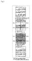
- FIG. 1 is a flowchart showing the operation of a CMP shape prediction simulator as a related art
- FIG. 2 is a schematic diagram showing an example of local processing for pattern density computation performed in the CMP shape prediction simulator shown in FIG. 1 ;
- FIG. 3 is a schematic diagram showing an example of distributed processing for pattern density computation performed in the CMP shape prediction simulator shown in FIG. 1 ;
- FIG. 4 is a schematic diagram showing the results of local processing and distributed processing applied to shape prediction computation performed in the CMP shape prediction simulator shown in FIG. 1 ;
- FIG. 5 is a block diagram showing a configuration of CMP shape prediction simulator which is a first embodiment
- FIG. 6 is a diagram showing a graph formed as a function that represents the range of effects that is caused when a pattern are polished with respect to two pads differing in hardness from each other;
- FIG. 7 is a schematic diagram showing divided regions assigned to CPUs in a case where a shape prediction objective region is divided into four to perform distributed processing;
- FIG. 8A is a schematic diagram showing an example of a case where borders of one of the divided regions to which an overlap amount is added coincide with grid lines;
- FIG. 8B is a schematic diagram showing an example of a case where the borders of one of the divided regions to which the overlap amount is added do not coincide with grid lines;
- FIG. 9 is a flowchart showing an example of a procedure for shape prediction processing performed in the CMP shape prediction simulator shown in FIG. 5 ;
- FIG. 10 is a schematic diagram showing the results of shape prediction computation processing (distributed processing) in the CMP shape prediction simulator in the first embodiment and the results of shape prediction computation processing (local processing) by one CPU referred to as a comparative example;
- FIG. 11 is a diagram showing a relationship between a program and hardware (computer) according to the present invention.
- FIG. 12 is a diagram showing another relationship between a program and hardware (computer) according to the present invention.
- a CMP shape prediction simulator includes: pattern density computation condition setting section 1 , pattern density computation section 2 , processing condition setting section 3 , overlap amount definition section 4 , shape prediction computation section 5 , merging processing section 6 and analysis section 7 .
- the computer system is constituted by a storage device for storing a program, etc., an input device such as a keyboard or a mouse, a display device such as a liquid crystal display (LCD), a communication device such as a modem for performing communication with an external device, an output device such as a printer, and a controller which operates in accordance with a program stored in the storage device and which controls the operations of the communication device, the output device and the display device while accepting inputs from the input device.
- a storage device for storing a program, etc.
- an input device such as a keyboard or a mouse
- a display device such as a liquid crystal display (LCD)
- a communication device such as a modem for performing communication with an external device
- an output device such as a printer
- a controller which operates in accordance with a program stored in the storage device and which controls the operations of the communication device, the output device and the display device while accepting inputs from the input device.
- Pattern density computation condition setting section 1 sets conditions for computation of the pattern density in a semiconductor device to be polished.
- pattern density computation condition setting section 1 displays, on the display device, layout data (a design drawing) which is information on the design of the semiconductor device.
- layout data a design drawing
- a simulator operator designates, by means of the input device, an analysis area on which a shape prediction is to be made by referring to the displayed layout data, and sets a computation resolution.
- the analysis area the whole or part of the design drawing can be designated.
- Pattern density computation section 2 extracts the pattern density in the designated analysis area on the basis of the computation conditions supplied from pattern density computation condition setting section 1 .
- this pattern density extraction processing either of two processes, i.e., local processing in which computation processing is performed by one CPU (see step S 11 in FIG. 1 ) and distributed processing in which computation processing is performed by a plurality of CPUs (see step S 12 in FIG. 1 ), is applied.
- the simulator operator performs a predetermined input operation on the input device to select local processing or distributed processing.
- high-efficiency computation processing can be performed.
- Pattern density extraction results are supplied from pattern density computation section 2 to shape prediction computation section 5 .
- Processing condition setting section 3 sets process conditions such as a model selection and a processing time for making a shape prediction.
- a model is formed (as an equation) so as to have polishing characteristics (polishing behaviors) with respect to conditions such as the pattern density and the wiring line width.
- polishing characteristics polishing behaviors
- Processing condition setting section 3 displays tool information on the display device, and the simulator operator designates the model for making a shape prediction from the displayed tool information by means of the input device.
- the simulator operator also sets a processing time corresponding to a polishing time by means of the input device.
- Overlap amount definition section 4 defines the amount of overlap between divided regions when a shape prediction objective region is divided into these regions. More specifically, overlap amount definition section 4 forms a function that represents the range of effects that is caused when a pattern is polished. Overlap amount definition section 4 defines, as an overlap amount, the half-width of a graph which shows, at the time of polishing, changes in pressure in the range of effects. The range of effects is dependent on the characteristics of a member used in chemical mechanical polishing. The graph is obtained based on a function of the range of effects.
- an overlap amount is determined on the basis of a characteristic diagram (graph) which is obtained from film thickness data and sectional shapes when the semiconductor device is actually polished under the “process conditions and member configuration” for the objective process, and the diagram is formed as a function that represents the range of effects that is caused by polishing the pattern.
- the member configuration means a member such as a polishing pad used in the CMP process.
- FIG. 6 shows, with respect to two pads differing in hardness, a graph formed as a function that represents the range of effects that is caused by polishing on the pattern when the semiconductor device is polished.
- the hardness of pad A in the two pads is smaller than that of the other pad B.
- the ordinate represents pressure and the abscissa represents an effect region.
- the effect region represents a region in which the pressure is changed.
- the effect region that is obtained when a pattern is polished with pad A is larger than the effect region that is obtained when a pattern is polished with pad B.
- the half-width a of the effect region is defined as an overlap amount.
- the half-width b of the effect region is defined as an overlap amount.
- the overlap amount (half-width) is supplied from overlap amount definition section 4 to shape prediction computation section 5 .
- Shape prediction computation section 5 performs computation processing for shape prediction in the case of polishing the semiconductor device on the basis of the pattern density extraction results supplied from pattern density computation section 2 , the process conditions supplied from processing condition setting section 3 and the overlap amount (half-width) supplied from overlap amount definition section 4 .
- the shape prediction objective region (objective figure) is divided into a plurality of regions in such a form that the overlap amount defined by the half-widths is added thereto.
- the divided regions are respectively assigned to the independent CPUs.
- Each CPU divides the assigned region into a plurality of regions in grid form and performs shape prediction computation processing on each divided region.
- FIG. 7 schematically shows divided regions assigned to the CPUs in a case where distributed processing is performed by dividing the region set as an object on which computation processing is to be performed (shape prediction objective region) into four.
- the region set as an object on which computation processing is to be performed is divided into first to the fourth divided regions.
- an overlapping portion A having a width corresponding to the overlap amount (half-width) supplied from overlap amount definition section 4 is added.
- the first divided region including the overlapping portion A is assigned to the first CPU ( 1 ).
- an overlapping portion B having a width corresponding to the overlap amount (half-width) supplied from overlap amount definition section 4 is added.
- the second divided region including the overlapping portion B is assigned to the second CPU ( 2 ).
- an overlapping portion C having a width corresponding to the overlap amount (half-width) supplied from overlap amount definition section 4 is added.
- the third divided region including the overlapping portion C is assigned to the third CPU ( 3 ).
- an overlapping portion D having a width corresponding to the overlap amount (half-width) supplied from overlap amount definition section 4 is added.
- the fourth divided region including the overlapping portion D is assigned to the fourth CPU ( 4 ).
- each of the first to fourth CPUs divides the assigned region into a plurality of regions in grid form and performs shape prediction computation processing on each divided region.
- FIG. 8A schematically shows an example of a case where borders of one of the divided regions to which the overlap amount is added coincide with grid lines.
- processing for expanding the divided region is not performed by shape prediction computation section 5 .
- FIG. 8B schematically shows an example of a case where borders of one of the divided regions to which the overlap amount is added do not coincide with grid lines.
- borders of the region to which the overlap amount is added do not coincide with the grid line.
- shape prediction computation section 5 performs processing for further expanding the divided region to which the overlap amount is added in each of the X-axis and Y-axis directions.
- the borders of the expanded region coincide with the grid lines.
- expansion processing with respect to the X-axis direction is performed.
- expansion processing with respect to the Y-axis direction is performed.
- Merging processing section 6 synthesizes a figure based on the results (predicted values) of shape prediction on the divided regions supplied from shape prediction computation section 5 .
- the results (predicted values) of shape prediction on the overlapping regions become unnecessary after merging processing. Therefore, merging processing section 6 removes the results (predicted values) of shape prediction on each overlapping region from the results (predicted values) of shape prediction on the corresponding divided region before performing figure synthesis.
- the merging processing results are supplied from merging processing section 6 to analysis section 7 .
- Analysis section 7 performs analysis processing on the basis of the merging processing results supplied from merging processing section 6 .
- analysis processing analysis of, for example, the film thickness in the designated analysis area is performed on the basis of the merging processing results.
- FIG. 9 shows an example of a shape prediction processing procedure.
- pattern density computation condition setting section 1 first sets conditions for computation of the pattern density in a semiconductor device to be polished (step S 20 ).
- Pattern density computation section 2 then extracts the pattern density in a designated analysis area on the basis of the computation conditions supplied from pattern density computation condition setting section 1 (step S 21 ).
- processing condition setting section 3 sets process conditions (step S 22 ) and overlap amount definition section 4 defines an overlap amount (step S 23 ).
- Shape prediction computation section 5 performs computation processing (distributed processing) (step S 24 ) for predicting a shape in the case of polishing the semiconductor device on the basis of the pattern density extraction results extracted in step S 21 , the process conditions set in step S 22 and the overlap amount (half-width) defined in step S 23 .
- merging processing section 6 synthesizes a figure (step S 25 ) based on the results (predicted values) of shape prediction on the divided regions obtained by distributed processing in step S 24 .
- Analysis section 7 thereafter performs analysis processing on the basis of the results of merging processing in step S 25 .
- the processing (function) in each of the above-described constituent sections can be realized by the controller (CPU) executing a program stored in the storage device on the computer system constituting the CMP shape prediction simulator.
- the program may be stored in the storage device in advance.
- the program may alternatively be provided by means of a recording medium typified by a CD-ROM or a DVD.
- a device for writing information to the recording medium and for reading information from the recording medium is provided in the CMP shape prediction simulator.
- the program may alternatively be provided to the CMP shape prediction simulator via a network typified by the Internet.
- a function to perform communication over the network is provided in the CMP shape prediction simulator.
- shape prediction computation performed by considering the influence of device pattern elements extending across the boundaries between divided regions and the influence of device pattern elements in the vicinity of the boundaries is enabled by causing the divided regions to overlap each other, thus realizing shape prediction computation with high accuracy.
- FIG. 10 shows the results of shape prediction computation processing (distributed processing) in the CMP shape prediction simulator in the present embodiment and the results of shape prediction computation processing (local processing) that are obtained by one CPU referred to as a comparative example.
- a section on the left-hand side of FIG. 10 an example of local processing (the same as that shown in FIG. 4 ) and an example of distributed processing are shown together with figures on which the processing is performed.
- a graph is shown which shows the results of shape prediction by local processing and distributed processing and the values that were actually measured.
- the objective figure on which local processing is performed and the objective figure on which distributed processing is performed are identical to each other.
- the ordinate represents the height of a polished portion and the abscissa represents the range of analysis (scan length).
- the thickest line indicates variations in height of a polished portion in b-b′ of the figure on which distributed processing is performed
- the second thickest line indicates variations in height of a polished portion in a-a′ of the figure on which local processing is performed.
- the thinnest line indicates the actually measured values of the actually polished portion.
- the computation processing time in the case of local processing is 6720 seconds, while the computation processing time in the case of distributed processing is 1932 seconds. Speed-up by about 3.5 times can be achieved by using distributed processing in comparison with local processing.
- the results of prediction by distributed processing are substantially the same as the actually measured values in the vicinity of the figure boundary (b-b′), and the shape prediction accuracy can be improved in comparison with distributed processing shown in FIG. 4 .
- CMP shape prediction simulator is an embodiment of the present invention.
- the configuration and the operation of the simulator can be changed as desired without departing from the gist of the invention.
- shape prediction computation processing section 5 may be configured so as to be capable of selecting between distributed processing and local processing.
- the simulator operator performs a predetermined input operation on the input device to select between local processing and distributed processing. Local processing is used for small-scale computation, while distributed processing is used for large-scale computation. Shape prediction computation processing can be performed with improved efficiency in this way.
- a CPU:A and CPUs: 1 to 4 are respectively connected to data bus 22 .
- the CPU:A can access a storage means in which program 20 and objective region 21 are stored.
- Program 20 makes the CPU:A execute first to fourth processings described below.
- the CPU:A first reads data on objective region 21 from the storage means (first processing). Subsequently, the CPU:A divides the read data into portions of a predetermined size, and forms a plurality of divided data groups by adding data corresponding to the overlap amount set in advance to the divided data portions (second processing). Subsequently, the CPU:A assigns the plurality of divided data groups to the CPUs: 1 to 4 , and each of the CPUs: 1 to 4 performs shape prediction processing (third processing).
- the number of CPUs which perform shape prediction processing is four in the present embodiment, the present invention is not limited to this.
- the number of CPUs may be smaller than four, or may be equal to or larger than five.
- the results of shape prediction on the objective region are output from the CPU:A.
- the CPU:A may be removed, as shown in FIG. 12 .
- one of the CPUs: 1 to 4 performs the first to fourth processing operations performed by CPU:A.
- the present invention can be applied to semiconductor manufacturing techniques and also to all shape prediction systems (or all figure processing apparatuses) for predicting the shape of a polished surface formed by chemical mechanical polishing, regardless of whether the polished surface is nonmetallic or metal-film-based.
Abstract
Description
Claims (9)
Applications Claiming Priority (2)
| Application Number | Priority Date | Filing Date | Title |
|---|---|---|---|
| JP2007-312470 | 2007-12-03 | ||
| JP2007312470A JP2009140956A (en) | 2007-12-03 | 2007-12-03 | Shape prediction simulator, method and program |
Publications (2)
| Publication Number | Publication Date |
|---|---|
| US20090144040A1 US20090144040A1 (en) | 2009-06-04 |
| US8073661B2 true US8073661B2 (en) | 2011-12-06 |
Family
ID=40676640
Family Applications (1)
| Application Number | Title | Priority Date | Filing Date |
|---|---|---|---|
| US12/326,575 Expired - Fee Related US8073661B2 (en) | 2007-12-03 | 2008-12-02 | Shape prediction simulator, method and program |
Country Status (2)
| Country | Link |
|---|---|
| US (1) | US8073661B2 (en) |
| JP (1) | JP2009140956A (en) |
Families Citing this family (1)
| Publication number | Priority date | Publication date | Assignee | Title |
|---|---|---|---|---|
| KR101781184B1 (en) | 2017-05-12 | 2017-10-10 | 한봉석 | Method and apparatus for analysis of polishing behavior in CMP process of semiconductor wafer |
Citations (11)
| Publication number | Priority date | Publication date | Assignee | Title |
|---|---|---|---|---|
| JPH098038A (en) | 1995-06-21 | 1997-01-10 | Mitsubishi Electric Corp | Simulation method for flatness |
| US6044213A (en) * | 1997-04-24 | 2000-03-28 | Nec Corporation | Process simulation method for calculating a surface oxidant concentration in oxidation process |
| JP3334796B2 (en) | 1999-04-20 | 2002-10-15 | 日本電気株式会社 | Polishing simulation method for semiconductor device |
| JP2003282495A (en) | 2002-03-26 | 2003-10-03 | Semiconductor Leading Edge Technologies Inc | Cmp process simulating method, program thereof and storage media |
| US20040248411A1 (en) * | 2001-08-22 | 2004-12-09 | Nikon Corporation | Method and device for simulation, method and device for polishing, method and device for preparing control parameters or control program, polishing system, recording medium, and method of manufacturing semiconductor device |
| US7216320B2 (en) * | 2003-11-06 | 2007-05-08 | Clear Shape Technologies, Inc. | Delta-geometry timing prediction in integrated circuit fabrication |
| US7360191B2 (en) * | 2003-11-06 | 2008-04-15 | Clear Shape Technologies, Inc. | Delta information design closure integrated circuit fabrication |
| US7549143B2 (en) * | 2003-06-24 | 2009-06-16 | Micron Technology, Inc. | Method and device for checking lithography data |
| US7648809B2 (en) * | 2005-08-17 | 2010-01-19 | Kabushiki Kaisha Toshiba | Electron beam exposure method, hot spot detecting apparatus, semiconductor device manufacturing method, and computer program product |
| US7686673B2 (en) * | 2001-01-31 | 2010-03-30 | Nikon Corporation | Working shape prediction method, working requirement determination method, working method, working system, method of manufacturing semiconductor device, computer program, and computer program storage medium |
| US7716628B2 (en) * | 2004-12-13 | 2010-05-11 | Kabushiki Kaisha Toshiba | System, method and program for generating mask data, exposure mask and semiconductor device in consideration of optical proximity effects |
Family Cites Families (3)
| Publication number | Priority date | Publication date | Assignee | Title |
|---|---|---|---|---|
| JPH11186205A (en) * | 1997-12-24 | 1999-07-09 | Sony Corp | Simulation method for processed surface height |
| JP2002140655A (en) * | 2000-11-02 | 2002-05-17 | Hitachi Ltd | Simulation for flattening semiconductor wafer |
| JP2007201256A (en) * | 2006-01-27 | 2007-08-09 | Renesas Technology Corp | Shape predicting method and system of semiconductor device |
-
2007
- 2007-12-03 JP JP2007312470A patent/JP2009140956A/en not_active Ceased
-
2008
- 2008-12-02 US US12/326,575 patent/US8073661B2/en not_active Expired - Fee Related
Patent Citations (13)
| Publication number | Priority date | Publication date | Assignee | Title |
|---|---|---|---|---|
| JPH098038A (en) | 1995-06-21 | 1997-01-10 | Mitsubishi Electric Corp | Simulation method for flatness |
| US6044213A (en) * | 1997-04-24 | 2000-03-28 | Nec Corporation | Process simulation method for calculating a surface oxidant concentration in oxidation process |
| JP3334796B2 (en) | 1999-04-20 | 2002-10-15 | 日本電気株式会社 | Polishing simulation method for semiconductor device |
| US7686673B2 (en) * | 2001-01-31 | 2010-03-30 | Nikon Corporation | Working shape prediction method, working requirement determination method, working method, working system, method of manufacturing semiconductor device, computer program, and computer program storage medium |
| US20100233937A1 (en) * | 2001-01-31 | 2010-09-16 | Tatsuya Senga | Method for predicting worked shape, method for determining working conditions, working method, working system, semiconductor device manufacturing method, computer program and computer program storage medium |
| US20040248411A1 (en) * | 2001-08-22 | 2004-12-09 | Nikon Corporation | Method and device for simulation, method and device for polishing, method and device for preparing control parameters or control program, polishing system, recording medium, and method of manufacturing semiconductor device |
| US7108580B2 (en) * | 2001-08-22 | 2006-09-19 | Nikon Corporation | Method and device for simulation, method and device for polishing, method and device for preparing control parameters or control program, polishing system, recording medium, and method of manufacturing semiconductor device |
| JP2003282495A (en) | 2002-03-26 | 2003-10-03 | Semiconductor Leading Edge Technologies Inc | Cmp process simulating method, program thereof and storage media |
| US7549143B2 (en) * | 2003-06-24 | 2009-06-16 | Micron Technology, Inc. | Method and device for checking lithography data |
| US7216320B2 (en) * | 2003-11-06 | 2007-05-08 | Clear Shape Technologies, Inc. | Delta-geometry timing prediction in integrated circuit fabrication |
| US7360191B2 (en) * | 2003-11-06 | 2008-04-15 | Clear Shape Technologies, Inc. | Delta information design closure integrated circuit fabrication |
| US7716628B2 (en) * | 2004-12-13 | 2010-05-11 | Kabushiki Kaisha Toshiba | System, method and program for generating mask data, exposure mask and semiconductor device in consideration of optical proximity effects |
| US7648809B2 (en) * | 2005-08-17 | 2010-01-19 | Kabushiki Kaisha Toshiba | Electron beam exposure method, hot spot detecting apparatus, semiconductor device manufacturing method, and computer program product |
Also Published As
| Publication number | Publication date |
|---|---|
| US20090144040A1 (en) | 2009-06-04 |
| JP2009140956A (en) | 2009-06-25 |
Similar Documents
| Publication | Publication Date | Title |
|---|---|---|
| Chen et al. | NTUplace3: An analytical placer for large-scale mixed-size designs with preplaced blocks and density constraints | |
| US20230267264A1 (en) | Hotspot Avoidance Method of Manufacturing Integrated Circuits | |
| JP2010272611A (en) | Method of manufacturing semiconductor device, apparatus for manufacturing semiconductor device, program of manufacturing semiconductor device, and program of generating mask data | |
| US11726837B2 (en) | Apparatus and method for providing workload distribution of threads among multiple compute units | |
| US8073661B2 (en) | Shape prediction simulator, method and program | |
| US8510685B1 (en) | Methods, systems, and articles of manufacture for creating a hierarchical output for an operation in an electronic design | |
| CN116484791A (en) | Method, apparatus and medium for graphics generation | |
| US8667433B2 (en) | Polishing estimation/evaluation device, overpolishing condition calculation device, and computer-readable non-transitory medium thereof | |
| KR101116786B1 (en) | Design verification apparatus for semiconductor device | |
| US9892226B2 (en) | Methods for providing macro placement of IC | |
| CN111611761B (en) | Method, apparatus and computer readable storage medium for generating circuit layout pattern | |
| US9435643B2 (en) | Presumably defective portion decision apparatus, presumably defective portion decision method, fabrication method for semiconductor device and program | |
| JP5609302B2 (en) | Contact definition device, contact definition program, and contact definition method | |
| US20100122226A1 (en) | Layout density verification system and layout density verification method | |
| WO2022100475A1 (en) | Back-side wafer modification | |
| JP4312671B2 (en) | Design rule check execution device | |
| US7107556B1 (en) | Method and system for implementing an analytical wirelength formulation for unavailability of routing directions | |
| WO2021205967A1 (en) | Hierarchical reduced-order matrix generation device | |
| KR100538103B1 (en) | Initial Structure Creation Method for 3D Semiconductor Process Simulation | |
| JP2001159809A (en) | Mask pattern designing device, mask pattern designing method and computer-readable recording medium storing mask pattern design program | |
| JP5609593B2 (en) | Semiconductor layout data design verification method and system | |
| JP2014089499A (en) | Layout designing method of semiconductor integrated circuit, layout design program, and layout design device | |
| JP2004258836A (en) | Semiconductor integrated circuit design method | |
| JP2007052725A (en) | Design device for semiconductor integrated circuit device, wiring method, and program | |
| JP2008305814A (en) | Method of designing semiconductor device, and semiconductor device |
Legal Events
| Date | Code | Title | Description |
|---|---|---|---|
| AS | Assignment |
Owner name: ELPIDA MEMORY, INC., JAPAN Free format text: ASSIGNMENT OF ASSIGNORS INTEREST;ASSIGNOR:TAKADA, YORIO;REEL/FRAME:021915/0430 Effective date: 20081127 |
|
| FEPP | Fee payment procedure |
Free format text: PAYOR NUMBER ASSIGNED (ORIGINAL EVENT CODE: ASPN); ENTITY STATUS OF PATENT OWNER: LARGE ENTITY |
|
| AS | Assignment |
Owner name: ELPIDA MEMORY INC., JAPAN Free format text: SECURITY AGREEMENT;ASSIGNOR:PS4 LUXCO S.A.R.L.;REEL/FRAME:032414/0261 Effective date: 20130726 |
|
| AS | Assignment |
Owner name: PS4 LUXCO S.A.R.L., LUXEMBOURG Free format text: ASSIGNMENT OF ASSIGNORS INTEREST;ASSIGNOR:ELPIDA MEMORY, INC.;REEL/FRAME:032899/0588 Effective date: 20130726 |
|
| REMI | Maintenance fee reminder mailed | ||
| LAPS | Lapse for failure to pay maintenance fees | ||
| STCH | Information on status: patent discontinuation |
Free format text: PATENT EXPIRED DUE TO NONPAYMENT OF MAINTENANCE FEES UNDER 37 CFR 1.362 |
|
| FP | Lapsed due to failure to pay maintenance fee |
Effective date: 20151206 |