US8054272B2 - Display apparatus - Google Patents
Display apparatus Download PDFInfo
- Publication number
- US8054272B2 US8054272B2 US12/412,070 US41207009A US8054272B2 US 8054272 B2 US8054272 B2 US 8054272B2 US 41207009 A US41207009 A US 41207009A US 8054272 B2 US8054272 B2 US 8054272B2
- Authority
- US
- United States
- Prior art keywords
- common voltage
- display
- line
- peripheral area
- power supply
- Prior art date
- Legal status (The legal status is an assumption and is not a legal conclusion. Google has not performed a legal analysis and makes no representation as to the accuracy of the status listed.)
- Expired - Fee Related, expires
Links
Images


Classifications
-
- G—PHYSICS
- G02—OPTICS
- G02F—OPTICAL DEVICES OR ARRANGEMENTS FOR THE CONTROL OF LIGHT BY MODIFICATION OF THE OPTICAL PROPERTIES OF THE MEDIA OF THE ELEMENTS INVOLVED THEREIN; NON-LINEAR OPTICS; FREQUENCY-CHANGING OF LIGHT; OPTICAL LOGIC ELEMENTS; OPTICAL ANALOGUE/DIGITAL CONVERTERS
- G02F1/00—Devices or arrangements for the control of the intensity, colour, phase, polarisation or direction of light arriving from an independent light source, e.g. switching, gating or modulating; Non-linear optics
- G02F1/01—Devices or arrangements for the control of the intensity, colour, phase, polarisation or direction of light arriving from an independent light source, e.g. switching, gating or modulating; Non-linear optics for the control of the intensity, phase, polarisation or colour
- G02F1/13—Devices or arrangements for the control of the intensity, colour, phase, polarisation or direction of light arriving from an independent light source, e.g. switching, gating or modulating; Non-linear optics for the control of the intensity, phase, polarisation or colour based on liquid crystals, e.g. single liquid crystal display cells
- G02F1/133—Constructional arrangements; Operation of liquid crystal cells; Circuit arrangements
- G02F1/136—Liquid crystal cells structurally associated with a semi-conducting layer or substrate, e.g. cells forming part of an integrated circuit
-
- G—PHYSICS
- G09—EDUCATION; CRYPTOGRAPHY; DISPLAY; ADVERTISING; SEALS
- G09G—ARRANGEMENTS OR CIRCUITS FOR CONTROL OF INDICATING DEVICES USING STATIC MEANS TO PRESENT VARIABLE INFORMATION
- G09G3/00—Control arrangements or circuits, of interest only in connection with visual indicators other than cathode-ray tubes
- G09G3/20—Control arrangements or circuits, of interest only in connection with visual indicators other than cathode-ray tubes for presentation of an assembly of a number of characters, e.g. a page, by composing the assembly by combination of individual elements arranged in a matrix no fixed position being assigned to or needed to be assigned to the individual characters or partial characters
- G09G3/34—Control arrangements or circuits, of interest only in connection with visual indicators other than cathode-ray tubes for presentation of an assembly of a number of characters, e.g. a page, by composing the assembly by combination of individual elements arranged in a matrix no fixed position being assigned to or needed to be assigned to the individual characters or partial characters by control of light from an independent source
- G09G3/36—Control arrangements or circuits, of interest only in connection with visual indicators other than cathode-ray tubes for presentation of an assembly of a number of characters, e.g. a page, by composing the assembly by combination of individual elements arranged in a matrix no fixed position being assigned to or needed to be assigned to the individual characters or partial characters by control of light from an independent source using liquid crystals
- G09G3/3611—Control of matrices with row and column drivers
- G09G3/3648—Control of matrices with row and column drivers using an active matrix
- G09G3/3655—Details of drivers for counter electrodes, e.g. common electrodes for pixel capacitors or supplementary storage capacitors
-
- G—PHYSICS
- G02—OPTICS
- G02F—OPTICAL DEVICES OR ARRANGEMENTS FOR THE CONTROL OF LIGHT BY MODIFICATION OF THE OPTICAL PROPERTIES OF THE MEDIA OF THE ELEMENTS INVOLVED THEREIN; NON-LINEAR OPTICS; FREQUENCY-CHANGING OF LIGHT; OPTICAL LOGIC ELEMENTS; OPTICAL ANALOGUE/DIGITAL CONVERTERS
- G02F1/00—Devices or arrangements for the control of the intensity, colour, phase, polarisation or direction of light arriving from an independent light source, e.g. switching, gating or modulating; Non-linear optics
- G02F1/01—Devices or arrangements for the control of the intensity, colour, phase, polarisation or direction of light arriving from an independent light source, e.g. switching, gating or modulating; Non-linear optics for the control of the intensity, phase, polarisation or colour
- G02F1/13—Devices or arrangements for the control of the intensity, colour, phase, polarisation or direction of light arriving from an independent light source, e.g. switching, gating or modulating; Non-linear optics for the control of the intensity, phase, polarisation or colour based on liquid crystals, e.g. single liquid crystal display cells
- G02F1/133—Constructional arrangements; Operation of liquid crystal cells; Circuit arrangements
- G02F1/1333—Constructional arrangements; Manufacturing methods
- G02F1/1345—Conductors connecting electrodes to cell terminals
-
- G—PHYSICS
- G02—OPTICS
- G02F—OPTICAL DEVICES OR ARRANGEMENTS FOR THE CONTROL OF LIGHT BY MODIFICATION OF THE OPTICAL PROPERTIES OF THE MEDIA OF THE ELEMENTS INVOLVED THEREIN; NON-LINEAR OPTICS; FREQUENCY-CHANGING OF LIGHT; OPTICAL LOGIC ELEMENTS; OPTICAL ANALOGUE/DIGITAL CONVERTERS
- G02F1/00—Devices or arrangements for the control of the intensity, colour, phase, polarisation or direction of light arriving from an independent light source, e.g. switching, gating or modulating; Non-linear optics
- G02F1/01—Devices or arrangements for the control of the intensity, colour, phase, polarisation or direction of light arriving from an independent light source, e.g. switching, gating or modulating; Non-linear optics for the control of the intensity, phase, polarisation or colour
- G02F1/13—Devices or arrangements for the control of the intensity, colour, phase, polarisation or direction of light arriving from an independent light source, e.g. switching, gating or modulating; Non-linear optics for the control of the intensity, phase, polarisation or colour based on liquid crystals, e.g. single liquid crystal display cells
- G02F1/133—Constructional arrangements; Operation of liquid crystal cells; Circuit arrangements
- G02F1/1333—Constructional arrangements; Manufacturing methods
- G02F1/1339—Gaskets; Spacers; Sealing of cells
- G02F1/13394—Gaskets; Spacers; Sealing of cells spacers regularly patterned on the cell subtrate, e.g. walls, pillars
-
- G—PHYSICS
- G02—OPTICS
- G02F—OPTICAL DEVICES OR ARRANGEMENTS FOR THE CONTROL OF LIGHT BY MODIFICATION OF THE OPTICAL PROPERTIES OF THE MEDIA OF THE ELEMENTS INVOLVED THEREIN; NON-LINEAR OPTICS; FREQUENCY-CHANGING OF LIGHT; OPTICAL LOGIC ELEMENTS; OPTICAL ANALOGUE/DIGITAL CONVERTERS
- G02F2201/00—Constructional arrangements not provided for in groups G02F1/00 - G02F7/00
- G02F2201/12—Constructional arrangements not provided for in groups G02F1/00 - G02F7/00 electrode
- G02F2201/121—Constructional arrangements not provided for in groups G02F1/00 - G02F7/00 electrode common or background
-
- G—PHYSICS
- G02—OPTICS
- G02F—OPTICAL DEVICES OR ARRANGEMENTS FOR THE CONTROL OF LIGHT BY MODIFICATION OF THE OPTICAL PROPERTIES OF THE MEDIA OF THE ELEMENTS INVOLVED THEREIN; NON-LINEAR OPTICS; FREQUENCY-CHANGING OF LIGHT; OPTICAL LOGIC ELEMENTS; OPTICAL ANALOGUE/DIGITAL CONVERTERS
- G02F2202/00—Materials and properties
- G02F2202/16—Materials and properties conductive
-
- G—PHYSICS
- G09—EDUCATION; CRYPTOGRAPHY; DISPLAY; ADVERTISING; SEALS
- G09G—ARRANGEMENTS OR CIRCUITS FOR CONTROL OF INDICATING DEVICES USING STATIC MEANS TO PRESENT VARIABLE INFORMATION
- G09G2300/00—Aspects of the constitution of display devices
- G09G2300/04—Structural and physical details of display devices
- G09G2300/0421—Structural details of the set of electrodes
- G09G2300/0426—Layout of electrodes and connections
-
- G—PHYSICS
- G09—EDUCATION; CRYPTOGRAPHY; DISPLAY; ADVERTISING; SEALS
- G09G—ARRANGEMENTS OR CIRCUITS FOR CONTROL OF INDICATING DEVICES USING STATIC MEANS TO PRESENT VARIABLE INFORMATION
- G09G2300/00—Aspects of the constitution of display devices
- G09G2300/04—Structural and physical details of display devices
- G09G2300/0421—Structural details of the set of electrodes
- G09G2300/043—Compensation electrodes or other additional electrodes in matrix displays related to distortions or compensation signals, e.g. for modifying TFT threshold voltage in column driver
-
- G—PHYSICS
- G09—EDUCATION; CRYPTOGRAPHY; DISPLAY; ADVERTISING; SEALS
- G09G—ARRANGEMENTS OR CIRCUITS FOR CONTROL OF INDICATING DEVICES USING STATIC MEANS TO PRESENT VARIABLE INFORMATION
- G09G2320/00—Control of display operating conditions
- G09G2320/02—Improving the quality of display appearance
- G09G2320/0219—Reducing feedthrough effects in active matrix panels, i.e. voltage changes on the scan electrode influencing the pixel voltage due to capacitive coupling
-
- G—PHYSICS
- G09—EDUCATION; CRYPTOGRAPHY; DISPLAY; ADVERTISING; SEALS
- G09G—ARRANGEMENTS OR CIRCUITS FOR CONTROL OF INDICATING DEVICES USING STATIC MEANS TO PRESENT VARIABLE INFORMATION
- G09G2320/00—Control of display operating conditions
- G09G2320/02—Improving the quality of display appearance
- G09G2320/0223—Compensation for problems related to R-C delay and attenuation in electrodes of matrix panels, e.g. in gate electrodes or on-substrate video signal electrodes
Definitions
- the present disclosure relates to a display apparatus. More particularly, the present disclosure relates to a display apparatus having improved image display quality.
- a liquid crystal display displays desired images by forming an electric field between two substrates and adjusting the amount of light passing through liquid crystals interposed between the two substrates.
- a plurality of gate lines, a plurality of data lines and a plurality of pixels may be provided at a lower substrate of the two substrates and a common electrode may be provided at an upper substrate of the two substrates.
- the liquid crystal display may sequentially drive the gate lines such that a data voltage applied to the data lines is provided to the pixels connected to the gate lines.
- a signal delay may occur in the gate lines due to a parasitic capacitance and an interconnection resistance.
- the signal delay may cause voltage of a data line to shift. This shift in voltage may be referred to as a kickback voltage, which can cause a flicker in a screen of the liquid crystal display.
- a display apparatus includes a gate driver, a data driver, a display panel, a power supply and a common voltage line.
- the gate driver outputs gate signals
- the data driver outputs data signals.
- the display panel includes a display area to display images in response to the gate signal and the data signal, and a peripheral area surrounding the display area.
- the peripheral area includes a first peripheral area disposed above the display area and a second peripheral area disposed below the display area.
- the power supply generates a common voltage and supplies the common voltage to the display panel.
- the common voltage line is disposed through the peripheral area and surrounds the display area.
- the common voltage line has two ends adjacent to the power supply. One of the two ends, which is disposed farther away from the gate driver than the other one of the two ends, is connected to the power supply to receive the common voltage.
- the display panel may include a spacer interposed between the common voltage line and the common electrode.
- the spacer may overlap the common voltage line such that the spacer is connected to the common electrode.
- the end of the common voltage line disposed farther away from the gate driver may be connected to the power supply and may receive the common voltage such that the common voltage may be differentially applied to the display panel according to a length of the common voltage line.
- a display apparatus in another exemplary embodiment of the present invention, includes a display panel, a power supply, a common voltage line, and at least one spacer.
- the display panel includes a display area to display an image and a peripheral area surrounding the display area.
- the power supply generates a common voltage and supplies the common voltage to the display panel.
- the display panel includes a first substrate, a second substrate facing the first substrate, and a liquid crystal layer interposed between the first substrate and the second substrate.
- the common voltage line is disposed through the peripheral area surrounding the display area.
- the spacers are interposed between the first substrate and the second substrate and overlap the common voltage line.
- the display apparatus may further include a pad electrode disposed between the common voltage line and each spacer. Each spacer may comprise a material having a polygonal prism shape to electrically connect a corresponding pad electrode to the common electrode.
- the display apparatus may further include a feedback line, and a common voltage compensator.
- the feedback line may be disposed in the peripheral area and provide a common voltage feedback.
- the common voltage compensator may generate a compensation signal based on the common voltage feedback.
- the power supply may generate a compensated common voltage based on the compensation signal and provide the compensating common voltage to the common voltage line.
- a display apparatus in another exemplary embodiment of the present invention, includes a gate driver, a data driver, a display panel, a power supply and a common voltage line.
- the gate driver outputs gate signals
- the data driver outputs data signals.
- the display panel includes a display area to display images in response to the gate signal and the data signal, and a peripheral area surrounding the display area.
- the peripheral area includes a first peripheral area disposed at a first side of the display area and a second peripheral area disposed at a second side opposing to the first side with respect to the display area.
- the power supply generates a common voltage and supplies the common voltage to the display panel.
- the common voltage line is disposed through the peripheral area and surrounds the display area.
- the common voltage line has two ends adjacent to the power supply. One of the two ends, which is disposed farther away from the gate driver than the other one of the two ends, is connected to the power supply to receive the common voltage.
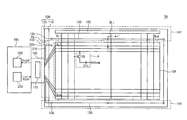
- FIG. 1 is a view showing a display apparatus according to an exemplary embodiment of the present invention
- FIG. 2 is an enlarged sectional view of a portion A shown in FIG. 1 ;
- FIG. 3 is a sectional view taken along line I-I′ shown in FIG. 1 .
- FIG. 1 is a view showing a display apparatus according to an exemplary embodiment of the present invention
- FIG. 2 is an enlarged sectional view of a portion A shown in FIG. 1
- FIG. 3 is a sectional view taken along line I-I′ shown in FIG. 1 .
- a display apparatus 10 includes a display panel 100 , a gate driver 150 , a data driver 170 and a power supply 200 .
- the display panel 100 includes a display area DA displaying an image and a peripheral area PA surrounding the display area DA.
- the display panel 100 includes a color filter substrate 110 , an array substrate 120 facing the color filter substrate 110 , and liquid crystals 119 interposed between the color filter substrate 110 and the array substrate 120 .
- the color filter substrate 110 includes a first base substrate 111 , a color filter 113 , and a common electrode 115 .
- the color filter substrate 110 is coupled to the array substrate 120 .
- the color filter 113 and the common electrode 115 are provided on a first base substrate 111 .
- the color filter 113 may include color pixels having red, green and blue colors.
- the common electrode 115 may be formed on the entire surface of the color filter substrate 110 .
- the common electrode 115 may receive a common voltage Vcom from an external source.
- a plurality of pixels are arranged in the display area DA of the array substrate 120 in a matrix pattern.
- a plurality of gate lines GL 1 to GLm and a plurality of data lines DL 1 to DLn are arranged in the display area DA of a second base substrate 121 .
- the gate lines GL 1 to GLm extend in a first direction and are spaced apart from each other at regular intervals.
- the data lines DL 1 to DLn extend in a second direction substantially perpendicular to the first direction and are spaced apart from each other at regular intervals.
- the gate lines GL 1 to GLm and the data lines DL 1 to DLn are provided on different layers.
- the gate lines GL 1 to GLm are insulated from the data lines DL 1 to DLn while crossing the data lines DL 1 to DLn.
- a plurality of pixel areas are defined on the display area DA by the gate lines GL 1 to GLm and the data lines DL 1 to DLn. Pixels are arranged in the pixel areas, respectively.
- Each pixel includes a thin film transistor 128 and a pixel electrode 132 .
- the pixel electrode 132 is connected to the thin film transistor 128 and generates an electric field in cooperation with the common electrode 115 to form a liquid crystal capacitor C 1 c.
- the thin film transistor 128 includes a gate electrode 122 provided on the second base substrate 121 , an insulating layer 123 provided on the gate electrode 122 , a semiconductor layer 124 overlapping the gate electrode 122 , and source and drain electrodes 125 and 126 that are provided on the insulating layer 123 and the semiconductor layer 124 .
- the thin film transistor 128 is protected from external impacts by a protection layer 129 .
- the pixel electrode 132 is connected to the drain electrode 126 through a first contact hole 131 formed through the protection layer 129 .
- the peripheral area PA of the array substrate 120 includes a first section 141 in which the gate driver 150 is arranged, a second section 143 to which the data driver 170 is connected, and a third section 145 facing the first section 141 , where the display area DA is interposed between the first and third sections 141 and 145 .
- a common voltage line 130 and a conductive spacer 135 are provided in the peripheral area PA.
- the common voltage line 130 surrounds the display area DA.
- the common voltage line 130 is arranged in the first section 141 to cross the gate lines GL 1 to GLm.
- the common voltage line 130 may be disposed on the same layer as the data lines GL 1 to GLn.
- the common voltage line 130 may cross a j th gate line GLj while the insulating layer 123 is interposed therebetween, and the common voltage line 130 may be disposed in parallel to the first data line DL 1 .
- the conductive spacer 135 is interposed between the array substrate 120 and the color filter substrate 110 .
- the conductive spacer 135 overlaps the common voltage line 130 .
- a conductive spacer 135 may be disposed on each pad electrode 134 connected to the common voltage line 130 .
- FIG. 1 illustrates use of several conductive spacers 135 .
- the pad electrode 134 is connected to the common voltage line 130 through a second contact hole 133 formed through the protection layer 129 .
- the pad electrode 134 may be formed on the same layer as the pixel electrode 132 .
- the conductive spacer 135 may include a conductive material having a polygonal prism shape to electrically connect the pad electrode 134 to the common electrode 115 .
- the gate driver 150 may include an amorphous silicon transistor formed in the first section 141 .
- the gate driver 150 may be directly formed together with the thin film transistor 128 on the array substrate 120 .
- the gate driver 150 is provided in the peripheral area PA to sequentially apply a gate signal including a gate on voltage and a gate off voltage to the gate lines GL 1 to GLm.
- the data driver 170 may be a single chip and may be mounted on a flexible circuit film 180 .
- the data driver 170 is connected to the data lines DL 1 to DLn provided in the second section 143 through the flexible circuit film 180 .
- the flexible circuit film 180 includes a flexible material and is provided with a plurality of interconnections to transmit the signal.
- the data driver 170 provides a data signal to the data lines DL 1 to DLn.
- the data driver 170 can invert a polarity of the data signal applied to the pixel electrode 132 .
- the power supply 200 may be mounted on a printed circuit board 190 such that the printed circuit board 190 is electrically connected to the flexible circuit film 180 on which the data driver 170 is mounted.
- the power supply 200 supplies the DC common voltage Vcom to the common voltage line 130 through the flexible circuit film 180 .
- the power supply 200 provides a drive voltage to the gate driver 150 and the data driver 170 .
- the printed circuit board 190 on which the power supply 200 is mounted, includes an interconnection provided to transmit the signal and a pad electrode connected to the flexible circuit film 180 .
- the display apparatus 10 further includes a feedback line 210 provided in the peripheral area PA of the array substrate 120 and a common voltage compensator 220 provided to supply a compensation signal to the power supply 200 .
- the feedback line 210 provided in the peripheral area PA is connected to a feedback conductive spacer 205 .
- the feedback line 210 may be formed on the same layer as the common voltage line 130 such that the feedback line 210 is connected to the flexible circuit film 180 .
- the feedback line 210 provides a common voltage feedback VcomF to the common voltage compensator 220 .
- the common voltage compensator 220 receives the common voltage feedback VcomF from the feedback line 210 and extracts a ripple voltage included in the common voltage feedback VcomF.
- the common voltage compensator 220 may provide a compensation signal having a phase opposite to that of the ripple voltage to the power supply 200 . Accordingly, the power supply 200 may output the compensated common voltage Vcom.
- the common voltage compensator 220 may be provided in the power supply 200 or externally.
- the common voltage Vcom is differentially applied to the common electrode 115 according to a difference in a kickback voltage generated from the display panel 100 .
- the kickback voltage represents a voltage difference of the data signal occurring when the data signal is subject to a voltage shift caused by a parasitic capacitance between the gate electrode 122 and the drain electrode 126 in the thin film transistor 128 .
- the kickback voltage may be expressed Equation 1 as follows:
- Vk Cgd Clc + Cgd ⁇ ( Von - Voff ) , [ Equation ⁇ ⁇ 1 ] where the Vk represents the kickback voltage, and Cgd represents the parasitic capacitance between the gate electrode 122 and the drain electrode 126 . Further, C 1 c , Von and Voff represent the capacitance of the liquid crystal capacitor, the gate on voltage, and the gate off voltage, respectively.
- the voltage level of the gate on voltage Von is lowered proportionally to a distance relative to the first section 141 due to a resistance and the parasitic capacitance. Accordingly, a difference between the gate on voltage Von and the gate off voltage Voff is decreased along the gate lines GL 1 to GLm proportionally to the distance relative to the first section 141 . Since the kickback voltage Vk is proportional to the difference between the gate on voltage Von and the gate off voltage Voff, a first end of the gate lines GL 1 to GLm disposed in the first section 141 has a kickback voltage greater than that of a second end of the gate lines GL 1 to GLm adjacent to the third section 145 .
- the common voltage Vcom is differentially applied to the first section 141 and the third section 145 , respectively, to prevent a flicker generated by the kickback voltage Vk.
- the common voltage Vcom having a low level is applied to the first section 141 having a greater kickback voltage Vk and the common voltage Vcom having a high level is applied to the third section 143 having a smaller kickback voltage Vk. Since the common voltage Vcom having the high level is applied to the third section 145 having the smaller kickback voltage Vk, a coupling effect of the parasitic capacitor Cgd may be reduced, and thereby the flicker may be prevented.
- a first end of the common voltage line 130 disposed in the second section 143 is connected to the power supply 200 to apply the common voltage Vcom corresponding to the kickback voltage Vk.
- the common voltage line 130 surrounds the display area DA by sequentially passing over the first section 141 and the third section 145 , so that a second end of the common voltage line 130 is disposed in the second section 143 adjacent to the power supply 200 .
- the common voltage Vcom is decreased by a resistance and a parasitic capacitance of the common voltage line 130 from the first end to the second end of the common voltage line 130 . Accordingly, the common voltage line 130 applies the differential common voltage Vcom to the common electrode 115 through the conductive spacer 135 .
Landscapes
- Physics & Mathematics (AREA)
- Nonlinear Science (AREA)
- Engineering & Computer Science (AREA)
- General Physics & Mathematics (AREA)
- Chemical & Material Sciences (AREA)
- Crystallography & Structural Chemistry (AREA)
- Mathematical Physics (AREA)
- Optics & Photonics (AREA)
- Theoretical Computer Science (AREA)
- Computer Hardware Design (AREA)
- Power Engineering (AREA)
- Liquid Crystal (AREA)
- Microelectronics & Electronic Packaging (AREA)
- Control Of Indicators Other Than Cathode Ray Tubes (AREA)
- Liquid Crystal Display Device Control (AREA)
- Devices For Indicating Variable Information By Combining Individual Elements (AREA)
Applications Claiming Priority (3)
| Application Number | Priority Date | Filing Date | Title |
|---|---|---|---|
| KR1020080085401A KR101500680B1 (ko) | 2008-08-29 | 2008-08-29 | 표시 장치 |
| KR10-2008-0085401 | 2008-08-29 | ||
| KR10-2008-085401 | 2008-08-29 |
Publications (2)
| Publication Number | Publication Date |
|---|---|
| US20100053056A1 US20100053056A1 (en) | 2010-03-04 |
| US8054272B2 true US8054272B2 (en) | 2011-11-08 |
Family
ID=41724598
Family Applications (1)
| Application Number | Title | Priority Date | Filing Date |
|---|---|---|---|
| US12/412,070 Expired - Fee Related US8054272B2 (en) | 2008-08-29 | 2009-03-26 | Display apparatus |
Country Status (4)
| Country | Link |
|---|---|
| US (1) | US8054272B2 (ko) |
| JP (1) | JP5680282B2 (ko) |
| KR (1) | KR101500680B1 (ko) |
| CN (1) | CN101661723B (ko) |
Cited By (4)
| Publication number | Priority date | Publication date | Assignee | Title |
|---|---|---|---|---|
| US9430982B2 (en) | 2013-05-14 | 2016-08-30 | Samsung Display Co., Ltd. | Display apparatus |
| US20170084247A1 (en) * | 2015-09-21 | 2017-03-23 | Apple Inc. | Gate line layout configuration |
| US9626930B2 (en) | 2012-05-16 | 2017-04-18 | Samsung Display Co., Ltd. | Display device |
| US11158281B2 (en) | 2018-11-26 | 2021-10-26 | Fuzhou Boe Optoelectronics Technology Co., Ltd. | Display panel and driving method for driving the display panel |
Families Citing this family (20)
| Publication number | Priority date | Publication date | Assignee | Title |
|---|---|---|---|---|
| US8373729B2 (en) * | 2010-03-22 | 2013-02-12 | Apple Inc. | Kickback compensation techniques |
| KR101827554B1 (ko) * | 2011-02-07 | 2018-02-12 | 삼성디스플레이 주식회사 | 표시장치 |
| CN105679220B (zh) * | 2011-05-20 | 2020-04-07 | 群创光电股份有限公司 | 显示面板 |
| CN102789755B (zh) * | 2011-05-20 | 2016-04-27 | 群创光电股份有限公司 | 显示面板 |
| KR20120139409A (ko) * | 2011-06-17 | 2012-12-27 | 삼성디스플레이 주식회사 | 감마 데이터 보상 시스템, 이를 포함하는 표시 장치 및 감마 데이터 보상 방법 |
| KR101977592B1 (ko) | 2012-07-24 | 2019-05-13 | 엘지디스플레이 주식회사 | 공통전압 보상회로를 포함하는 액정표시장치 |
| CN102903344B (zh) * | 2012-09-27 | 2014-10-08 | 合肥京东方光电科技有限公司 | 公共电极电压补偿方法、装置及时序控制器 |
| CN104122690A (zh) * | 2013-08-23 | 2014-10-29 | 深超光电(深圳)有限公司 | 液晶显示装置以及显示装置 |
| CN103472646B (zh) * | 2013-08-30 | 2016-08-31 | 京东方科技集团股份有限公司 | 一种阵列基板及其制备方法和显示装置 |
| US9564455B2 (en) * | 2014-04-10 | 2017-02-07 | Innolux Corporation | Display panel |
| KR102196101B1 (ko) * | 2014-10-23 | 2020-12-30 | 삼성디스플레이 주식회사 | 표시 장치 |
| KR102170556B1 (ko) * | 2014-10-23 | 2020-10-28 | 엘지디스플레이 주식회사 | 표시장치 및 그 구동방법 |
| KR102284296B1 (ko) * | 2015-01-13 | 2021-08-03 | 삼성디스플레이 주식회사 | 표시 장치 및 이를 이용한 표시 패널의 구동 방법 |
| KR102364633B1 (ko) * | 2015-01-22 | 2022-02-17 | 엘지디스플레이 주식회사 | 표시장치 및 이의 구동방법 |
| CN104882092B (zh) * | 2015-06-29 | 2017-12-08 | 京东方科技集团股份有限公司 | 一种内嵌式触控显示屏及其驱动方法、显示装置 |
| US10380937B2 (en) * | 2015-08-26 | 2019-08-13 | Apple Inc. | Multi-zoned variable VCOM control |
| KR102438782B1 (ko) * | 2015-11-26 | 2022-09-01 | 엘지디스플레이 주식회사 | 표시장치와 이의 제조방법 |
| CN108694922B (zh) * | 2018-04-03 | 2020-11-03 | 昆山龙腾光电股份有限公司 | 公共电压驱动方法、装置及显示装置 |
| CN109036255A (zh) * | 2018-09-30 | 2018-12-18 | 厦门天马微电子有限公司 | 一种显示驱动方法、显示驱动装置和显示设备 |
| CN111243538B (zh) * | 2020-02-14 | 2022-08-09 | 京东方科技集团股份有限公司 | 显示面板的公共电压补偿方法及装置、显示面板和装置 |
Citations (20)
| Publication number | Priority date | Publication date | Assignee | Title |
|---|---|---|---|---|
| JPH11288001A (ja) | 1998-04-01 | 1999-10-19 | Citizen Watch Co Ltd | 液晶表示装置 |
| KR20010008893A (ko) | 1999-07-05 | 2001-02-05 | 구본준 | 액정표시장치의 킥백전압 보정방법. |
| US20040108985A1 (en) * | 2002-12-10 | 2004-06-10 | Song In Duk | Liquid crystal display panel of line-on glass type and method of fabricating the same |
| US6756958B2 (en) * | 2000-11-30 | 2004-06-29 | Hitachi, Ltd. | Liquid crystal display device |
| KR20050086921A (ko) | 2002-12-19 | 2005-08-30 | 코닌클리즈케 필립스 일렉트로닉스 엔.브이. | 디스플레이 영역 외측의 복수의 측정 화소에 대한 측정치에근거해 dc 전압 보상되는 액티브 매트릭스 디스플레이디바이스 |
| US20050212735A1 (en) * | 2004-03-29 | 2005-09-29 | Che-Li Lin | [driving circuit of liquid crystal display] |
| US7224353B2 (en) * | 2002-10-14 | 2007-05-29 | Lg.Philips Lcd Co., Ltd. | Liquid crystal display device and driving method thereof |
| KR20070060660A (ko) | 2005-12-09 | 2007-06-13 | 삼성전자주식회사 | 액정 표시 장치 |
| US7349055B2 (en) * | 2003-06-30 | 2008-03-25 | Lg.Philips Lcd Co., Ltd. | Line on glass type liquid crystal display device and method of fabricating the same |
| US20080136795A1 (en) * | 2005-03-25 | 2008-06-12 | Takaji Numao | Display Device and Driving Method Thereof |
| US20080273003A1 (en) * | 2007-03-26 | 2008-11-06 | Sang-Jin Jeon | Liquid crystal display device, manufacturing method thereof and driving method thereof |
| US7463324B2 (en) * | 2001-12-20 | 2008-12-09 | Lg Display Co., Ltd. | Liquid crystal display panel of line on glass type |
| US7502020B2 (en) * | 2003-12-30 | 2009-03-10 | Lg Display Co., Ltd. | Liquid crystal display device with voltage compensator |
| US7773187B2 (en) * | 2007-04-27 | 2010-08-10 | Hitachi Displays, Ltd. | Liquid crystal display device |
| US7786960B2 (en) * | 2004-06-30 | 2010-08-31 | Lg. Display Co., Ltd. | Liquid crystal display and driving method thereof |
| US7851996B2 (en) * | 2005-11-16 | 2010-12-14 | Canon Kabushiki Kaisha | Display apparatus |
| US7898514B2 (en) * | 2003-10-24 | 2011-03-01 | Lg Display Co., Ltd. | Apparatus for driving gate of liquid crystal display and driving method thereof |
| US7916134B2 (en) * | 2002-12-05 | 2011-03-29 | Seiko Epson Corporation | Power supply method and power supply circuit |
| US7956833B2 (en) * | 2006-06-16 | 2011-06-07 | Seiko Epson Corporation | Display driver, electro-optical device, and electronic instrument |
| US7961179B2 (en) * | 2006-09-28 | 2011-06-14 | Sanyo Electric Co., Ltd. | Integrated driving apparatus for display apparatus |
Family Cites Families (6)
| Publication number | Priority date | Publication date | Assignee | Title |
|---|---|---|---|---|
| JPH09218388A (ja) * | 1996-02-09 | 1997-08-19 | Hosiden Corp | 液晶表示装置 |
| JP4082282B2 (ja) * | 2003-06-06 | 2008-04-30 | ソニー株式会社 | 液晶表示装置および携帯端末 |
| JP2005070541A (ja) * | 2003-08-26 | 2005-03-17 | Seiko Epson Corp | 液晶表示装置及び携帯型電子機器 |
| JP2005250132A (ja) * | 2004-03-04 | 2005-09-15 | Sanyo Electric Co Ltd | アクティブマトリクス型液晶表示装置。 |
| JP2007212610A (ja) * | 2006-02-08 | 2007-08-23 | Seiko Epson Corp | 液晶表示装置、液晶表示パネル、及び液晶表示装置の製造方法 |
| KR101293569B1 (ko) * | 2006-08-03 | 2013-08-06 | 삼성디스플레이 주식회사 | 연성부재와 이를 포함하는 액정표시장치 |
-
2008
- 2008-08-29 KR KR1020080085401A patent/KR101500680B1/ko active IP Right Grant
-
2009
- 2009-03-26 US US12/412,070 patent/US8054272B2/en not_active Expired - Fee Related
- 2009-04-08 JP JP2009093633A patent/JP5680282B2/ja not_active Expired - Fee Related
- 2009-05-08 CN CN2009101364339A patent/CN101661723B/zh not_active Expired - Fee Related
Patent Citations (22)
| Publication number | Priority date | Publication date | Assignee | Title |
|---|---|---|---|---|
| JPH11288001A (ja) | 1998-04-01 | 1999-10-19 | Citizen Watch Co Ltd | 液晶表示装置 |
| KR20010008893A (ko) | 1999-07-05 | 2001-02-05 | 구본준 | 액정표시장치의 킥백전압 보정방법. |
| US6756958B2 (en) * | 2000-11-30 | 2004-06-29 | Hitachi, Ltd. | Liquid crystal display device |
| US7463324B2 (en) * | 2001-12-20 | 2008-12-09 | Lg Display Co., Ltd. | Liquid crystal display panel of line on glass type |
| US7224353B2 (en) * | 2002-10-14 | 2007-05-29 | Lg.Philips Lcd Co., Ltd. | Liquid crystal display device and driving method thereof |
| US7830371B2 (en) * | 2002-10-14 | 2010-11-09 | Lg Display Co., Ltd. | Liquid crystal display device and driving method thereof |
| US7750888B2 (en) * | 2002-10-14 | 2010-07-06 | Lg Display Co., Ltd. | Liquid crystal display device and driving method thereof |
| US7916134B2 (en) * | 2002-12-05 | 2011-03-29 | Seiko Epson Corporation | Power supply method and power supply circuit |
| US20040108985A1 (en) * | 2002-12-10 | 2004-06-10 | Song In Duk | Liquid crystal display panel of line-on glass type and method of fabricating the same |
| KR20050086921A (ko) | 2002-12-19 | 2005-08-30 | 코닌클리즈케 필립스 일렉트로닉스 엔.브이. | 디스플레이 영역 외측의 복수의 측정 화소에 대한 측정치에근거해 dc 전압 보상되는 액티브 매트릭스 디스플레이디바이스 |
| US7349055B2 (en) * | 2003-06-30 | 2008-03-25 | Lg.Philips Lcd Co., Ltd. | Line on glass type liquid crystal display device and method of fabricating the same |
| US7898514B2 (en) * | 2003-10-24 | 2011-03-01 | Lg Display Co., Ltd. | Apparatus for driving gate of liquid crystal display and driving method thereof |
| US7502020B2 (en) * | 2003-12-30 | 2009-03-10 | Lg Display Co., Ltd. | Liquid crystal display device with voltage compensator |
| US20050212735A1 (en) * | 2004-03-29 | 2005-09-29 | Che-Li Lin | [driving circuit of liquid crystal display] |
| US7786960B2 (en) * | 2004-06-30 | 2010-08-31 | Lg. Display Co., Ltd. | Liquid crystal display and driving method thereof |
| US20080136795A1 (en) * | 2005-03-25 | 2008-06-12 | Takaji Numao | Display Device and Driving Method Thereof |
| US7851996B2 (en) * | 2005-11-16 | 2010-12-14 | Canon Kabushiki Kaisha | Display apparatus |
| KR20070060660A (ko) | 2005-12-09 | 2007-06-13 | 삼성전자주식회사 | 액정 표시 장치 |
| US7956833B2 (en) * | 2006-06-16 | 2011-06-07 | Seiko Epson Corporation | Display driver, electro-optical device, and electronic instrument |
| US7961179B2 (en) * | 2006-09-28 | 2011-06-14 | Sanyo Electric Co., Ltd. | Integrated driving apparatus for display apparatus |
| US20080273003A1 (en) * | 2007-03-26 | 2008-11-06 | Sang-Jin Jeon | Liquid crystal display device, manufacturing method thereof and driving method thereof |
| US7773187B2 (en) * | 2007-04-27 | 2010-08-10 | Hitachi Displays, Ltd. | Liquid crystal display device |
Cited By (6)
| Publication number | Priority date | Publication date | Assignee | Title |
|---|---|---|---|---|
| US9626930B2 (en) | 2012-05-16 | 2017-04-18 | Samsung Display Co., Ltd. | Display device |
| US10332473B2 (en) | 2012-05-16 | 2019-06-25 | Samsung Display Co., Ltd. | Display device |
| US9430982B2 (en) | 2013-05-14 | 2016-08-30 | Samsung Display Co., Ltd. | Display apparatus |
| US20170084247A1 (en) * | 2015-09-21 | 2017-03-23 | Apple Inc. | Gate line layout configuration |
| US10170072B2 (en) * | 2015-09-21 | 2019-01-01 | Apple Inc. | Gate line layout configuration |
| US11158281B2 (en) | 2018-11-26 | 2021-10-26 | Fuzhou Boe Optoelectronics Technology Co., Ltd. | Display panel and driving method for driving the display panel |
Also Published As
| Publication number | Publication date |
|---|---|
| CN101661723A (zh) | 2010-03-03 |
| JP2010055059A (ja) | 2010-03-11 |
| CN101661723B (zh) | 2013-06-05 |
| KR20100026412A (ko) | 2010-03-10 |
| JP5680282B2 (ja) | 2015-03-04 |
| KR101500680B1 (ko) | 2015-03-10 |
| US20100053056A1 (en) | 2010-03-04 |
Similar Documents
| Publication | Publication Date | Title |
|---|---|---|
| US8054272B2 (en) | Display apparatus | |
| US10185195B2 (en) | Horizontal stripe liquid crystal display device | |
| KR102009388B1 (ko) | 액정 디스플레이 장치 | |
| KR101443380B1 (ko) | 액정표시장치 | |
| KR101204365B1 (ko) | 액정 표시 패널 및 그 제조 방법 | |
| US8395744B2 (en) | Display device including dummy pixel region | |
| US20110007257A1 (en) | Liquid crystal display | |
| KR101746862B1 (ko) | 액정표시장치 | |
| JP2007193334A5 (ko) | ||
| KR20110064114A (ko) | 액정표시장치 | |
| KR101046927B1 (ko) | 박막 트랜지스터 표시판 | |
| KR100531388B1 (ko) | 표시 장치 | |
| KR20080053644A (ko) | 액정 표시 장치 | |
| JPS6317432A (ja) | 平面デイスプレイ装置 | |
| KR20020095203A (ko) | 디스플레이 디바이스 | |
| KR20070081734A (ko) | 광학 보상용 복굴절 액정 표시 패널 | |
| KR20100008691A (ko) | 액정표시장치 | |
| KR100966438B1 (ko) | 스토리지 배선의 저항을 감소시킨 액정표시패널 | |
| JP2010091904A (ja) | 液晶表示装置 | |
| KR20080019800A (ko) | 액정표시장치의 어레이 기판 | |
| JP6164554B2 (ja) | 表示装置 | |
| KR102459724B1 (ko) | 액정표시장치 | |
| US20210263383A1 (en) | Display apparatus | |
| KR20070087331A (ko) | 액정 표시 장치 | |
| KR20080048688A (ko) | 액정 표시 장치 |
Legal Events
| Date | Code | Title | Description |
|---|---|---|---|
| AS | Assignment |
Owner name: SAMSUNG ELECTRONICS CO., LTD.,KOREA, DEMOCRATIC PE Free format text: ASSIGNMENT OF ASSIGNORS INTEREST;ASSIGNORS:LEE, CHANG-SOO;BAE, YU-HAN;REEL/FRAME:022457/0256 Effective date: 20090316 Owner name: SAMSUNG ELECTRONICS CO., LTD., KOREA, DEMOCRATIC P Free format text: ASSIGNMENT OF ASSIGNORS INTEREST;ASSIGNORS:LEE, CHANG-SOO;BAE, YU-HAN;REEL/FRAME:022457/0256 Effective date: 20090316 |
|
| STCF | Information on status: patent grant |
Free format text: PATENTED CASE |
|
| FEPP | Fee payment procedure |
Free format text: PAYOR NUMBER ASSIGNED (ORIGINAL EVENT CODE: ASPN); ENTITY STATUS OF PATENT OWNER: LARGE ENTITY |
|
| AS | Assignment |
Owner name: SAMSUNG DISPLAY CO., LTD., KOREA, REPUBLIC OF Free format text: ASSIGNMENT OF ASSIGNORS INTEREST;ASSIGNOR:SAMSUNG ELECTRONICS CO., LTD.;REEL/FRAME:029045/0860 Effective date: 20120904 |
|
| FPAY | Fee payment |
Year of fee payment: 4 |
|
| FEPP | Fee payment procedure |
Free format text: MAINTENANCE FEE REMINDER MAILED (ORIGINAL EVENT CODE: REM.); ENTITY STATUS OF PATENT OWNER: LARGE ENTITY |
|
| LAPS | Lapse for failure to pay maintenance fees |
Free format text: PATENT EXPIRED FOR FAILURE TO PAY MAINTENANCE FEES (ORIGINAL EVENT CODE: EXP.); ENTITY STATUS OF PATENT OWNER: LARGE ENTITY |
|
| STCH | Information on status: patent discontinuation |
Free format text: PATENT EXPIRED DUE TO NONPAYMENT OF MAINTENANCE FEES UNDER 37 CFR 1.362 |
|
| FP | Lapsed due to failure to pay maintenance fee |
Effective date: 20191108 |