US8030668B2 - Semiconductor LED, opto-electronic integrated circuits (OEIC), and method of fabricating OEIC - Google Patents
Semiconductor LED, opto-electronic integrated circuits (OEIC), and method of fabricating OEIC Download PDFInfo
- Publication number
- US8030668B2 US8030668B2 US11/935,904 US93590407A US8030668B2 US 8030668 B2 US8030668 B2 US 8030668B2 US 93590407 A US93590407 A US 93590407A US 8030668 B2 US8030668 B2 US 8030668B2
- Authority
- US
- United States
- Prior art keywords
- silicon
- light emitting
- waveguide
- semiconductor
- film
- Prior art date
- Legal status (The legal status is an assumption and is not a legal conclusion. Google has not performed a legal analysis and makes no representation as to the accuracy of the status listed.)
- Expired - Fee Related, expires
Links
- 239000004065 semiconductor Substances 0.000 title claims abstract description 112
- 238000004519 manufacturing process Methods 0.000 title description 7
- 230000005693 optoelectronics Effects 0.000 title description 3
- 229910052710 silicon Inorganic materials 0.000 claims abstract description 167
- 239000010703 silicon Substances 0.000 claims abstract description 166
- 239000000758 substrate Substances 0.000 claims abstract description 64
- 239000010409 thin film Substances 0.000 claims abstract description 35
- 239000000463 material Substances 0.000 claims abstract description 13
- 239000010408 film Substances 0.000 claims description 220
- 229910052581 Si3N4 Inorganic materials 0.000 claims description 54
- HQVNEWCFYHHQES-UHFFFAOYSA-N silicon nitride Chemical compound N12[Si]34N5[Si]62N3[Si]51N64 HQVNEWCFYHHQES-UHFFFAOYSA-N 0.000 claims description 54
- 238000009413 insulation Methods 0.000 claims description 22
- 230000007704 transition Effects 0.000 claims description 14
- 239000002178 crystalline material Substances 0.000 claims 2
- XUIMIQQOPSSXEZ-UHFFFAOYSA-N Silicon Chemical compound [Si] XUIMIQQOPSSXEZ-UHFFFAOYSA-N 0.000 abstract description 165
- 238000000034 method Methods 0.000 abstract description 103
- 230000008569 process Effects 0.000 abstract description 75
- 238000004020 luminiscence type Methods 0.000 abstract description 39
- 229910021419 crystalline silicon Inorganic materials 0.000 abstract description 21
- 229910052732 germanium Inorganic materials 0.000 abstract description 3
- GNPVGFCGXDBREM-UHFFFAOYSA-N germanium atom Chemical compound [Ge] GNPVGFCGXDBREM-UHFFFAOYSA-N 0.000 abstract description 3
- 239000010410 layer Substances 0.000 description 72
- VYPSYNLAJGMNEJ-UHFFFAOYSA-N Silicium dioxide Chemical compound O=[Si]=O VYPSYNLAJGMNEJ-UHFFFAOYSA-N 0.000 description 69
- 229910052814 silicon oxide Inorganic materials 0.000 description 41
- 229910052751 metal Inorganic materials 0.000 description 34
- 239000002184 metal Substances 0.000 description 34
- 239000012535 impurity Substances 0.000 description 30
- 230000015572 biosynthetic process Effects 0.000 description 27
- 230000003647 oxidation Effects 0.000 description 27
- 238000007254 oxidation reaction Methods 0.000 description 27
- 230000005428 wave function Effects 0.000 description 25
- 150000001875 compounds Chemical class 0.000 description 23
- 239000011229 interlayer Substances 0.000 description 17
- 238000005468 ion implantation Methods 0.000 description 17
- 239000013078 crystal Substances 0.000 description 16
- 238000002513 implantation Methods 0.000 description 14
- 239000000377 silicon dioxide Substances 0.000 description 14
- 235000012239 silicon dioxide Nutrition 0.000 description 13
- 150000004767 nitrides Chemical class 0.000 description 12
- 230000006870 function Effects 0.000 description 11
- 150000002500 ions Chemical class 0.000 description 11
- 229910021332 silicide Inorganic materials 0.000 description 11
- FVBUAEGBCNSCDD-UHFFFAOYSA-N silicide(4-) Chemical compound [Si-4] FVBUAEGBCNSCDD-UHFFFAOYSA-N 0.000 description 11
- 235000012431 wafers Nutrition 0.000 description 11
- 238000001312 dry etching Methods 0.000 description 10
- 230000003287 optical effect Effects 0.000 description 10
- 238000009792 diffusion process Methods 0.000 description 9
- 230000000694 effects Effects 0.000 description 9
- -1 e.g. Substances 0.000 description 8
- 238000012545 processing Methods 0.000 description 8
- 238000000137 annealing Methods 0.000 description 7
- 238000005229 chemical vapour deposition Methods 0.000 description 7
- 239000002245 particle Substances 0.000 description 7
- 229920002120 photoresistant polymer Polymers 0.000 description 7
- 229910052796 boron Inorganic materials 0.000 description 6
- 238000004891 communication Methods 0.000 description 6
- 230000005684 electric field Effects 0.000 description 6
- 238000004134 energy conservation Methods 0.000 description 6
- 238000010438 heat treatment Methods 0.000 description 6
- 239000000523 sample Substances 0.000 description 6
- 125000006850 spacer group Chemical group 0.000 description 6
- 230000004913 activation Effects 0.000 description 5
- 239000012298 atmosphere Substances 0.000 description 5
- 238000006243 chemical reaction Methods 0.000 description 5
- 238000000151 deposition Methods 0.000 description 5
- 239000012212 insulator Substances 0.000 description 5
- 239000011159 matrix material Substances 0.000 description 5
- 238000000206 photolithography Methods 0.000 description 5
- 229910021420 polycrystalline silicon Inorganic materials 0.000 description 5
- 230000005610 quantum mechanics Effects 0.000 description 5
- KRHYYFGTRYWZRS-UHFFFAOYSA-N Fluorane Chemical compound F KRHYYFGTRYWZRS-UHFFFAOYSA-N 0.000 description 4
- MHAJPDPJQMAIIY-UHFFFAOYSA-N Hydrogen peroxide Chemical compound OO MHAJPDPJQMAIIY-UHFFFAOYSA-N 0.000 description 4
- PXHVJJICTQNCMI-UHFFFAOYSA-N Nickel Chemical compound [Ni] PXHVJJICTQNCMI-UHFFFAOYSA-N 0.000 description 4
- NBIIXXVUZAFLBC-UHFFFAOYSA-N Phosphoric acid Chemical compound OP(O)(O)=O NBIIXXVUZAFLBC-UHFFFAOYSA-N 0.000 description 4
- 229910052785 arsenic Inorganic materials 0.000 description 4
- 238000010586 diagram Methods 0.000 description 4
- 230000003993 interaction Effects 0.000 description 4
- 239000005001 laminate film Substances 0.000 description 4
- 238000010030 laminating Methods 0.000 description 4
- 238000001459 lithography Methods 0.000 description 4
- 238000000059 patterning Methods 0.000 description 4
- 238000005424 photoluminescence Methods 0.000 description 4
- 238000001228 spectrum Methods 0.000 description 4
- 238000012360 testing method Methods 0.000 description 4
- OAICVXFJPJFONN-UHFFFAOYSA-N Phosphorus Chemical compound [P] OAICVXFJPJFONN-UHFFFAOYSA-N 0.000 description 3
- RQNWIZPPADIBDY-UHFFFAOYSA-N arsenic atom Chemical compound [As] RQNWIZPPADIBDY-UHFFFAOYSA-N 0.000 description 3
- 230000004888 barrier function Effects 0.000 description 3
- 230000008859 change Effects 0.000 description 3
- 230000008021 deposition Effects 0.000 description 3
- 230000005685 electric field effect Effects 0.000 description 3
- 238000002474 experimental method Methods 0.000 description 3
- 239000011521 glass Substances 0.000 description 3
- 125000005842 heteroatom Chemical group 0.000 description 3
- 238000005286 illumination Methods 0.000 description 3
- 230000010354 integration Effects 0.000 description 3
- 150000002739 metals Chemical class 0.000 description 3
- 239000005543 nano-size silicon particle Substances 0.000 description 3
- 229910052757 nitrogen Inorganic materials 0.000 description 3
- 230000010355 oscillation Effects 0.000 description 3
- 238000005498 polishing Methods 0.000 description 3
- 229910021426 porous silicon Inorganic materials 0.000 description 3
- 230000000644 propagated effect Effects 0.000 description 3
- 230000005476 size effect Effects 0.000 description 3
- 238000012795 verification Methods 0.000 description 3
- 238000001039 wet etching Methods 0.000 description 3
- IJGRMHOSHXDMSA-UHFFFAOYSA-N Atomic nitrogen Chemical compound N#N IJGRMHOSHXDMSA-UHFFFAOYSA-N 0.000 description 2
- ZOXJGFHDIHLPTG-UHFFFAOYSA-N Boron Chemical compound [B] ZOXJGFHDIHLPTG-UHFFFAOYSA-N 0.000 description 2
- 241000047703 Nonion Species 0.000 description 2
- 229910000577 Silicon-germanium Inorganic materials 0.000 description 2
- RTAQQCXQSZGOHL-UHFFFAOYSA-N Titanium Chemical compound [Ti] RTAQQCXQSZGOHL-UHFFFAOYSA-N 0.000 description 2
- LEVVHYCKPQWKOP-UHFFFAOYSA-N [Si].[Ge] Chemical compound [Si].[Ge] LEVVHYCKPQWKOP-UHFFFAOYSA-N 0.000 description 2
- 229910000147 aluminium phosphate Inorganic materials 0.000 description 2
- 229910021417 amorphous silicon Inorganic materials 0.000 description 2
- 238000013459 approach Methods 0.000 description 2
- 238000010420 art technique Methods 0.000 description 2
- 230000008901 benefit Effects 0.000 description 2
- 230000005540 biological transmission Effects 0.000 description 2
- 229910017052 cobalt Inorganic materials 0.000 description 2
- 239000010941 cobalt Substances 0.000 description 2
- GUTLYIVDDKVIGB-UHFFFAOYSA-N cobalt atom Chemical compound [Co] GUTLYIVDDKVIGB-UHFFFAOYSA-N 0.000 description 2
- 239000004020 conductor Substances 0.000 description 2
- 239000012792 core layer Substances 0.000 description 2
- 230000007423 decrease Effects 0.000 description 2
- 230000007547 defect Effects 0.000 description 2
- 238000005401 electroluminescence Methods 0.000 description 2
- 238000000572 ellipsometry Methods 0.000 description 2
- 238000005530 etching Methods 0.000 description 2
- 238000011156 evaluation Methods 0.000 description 2
- 230000005669 field effect Effects 0.000 description 2
- 238000009396 hybridization Methods 0.000 description 2
- 125000004435 hydrogen atom Chemical group [H]* 0.000 description 2
- 238000002955 isolation Methods 0.000 description 2
- 230000033001 locomotion Effects 0.000 description 2
- 230000007246 mechanism Effects 0.000 description 2
- 229910044991 metal oxide Inorganic materials 0.000 description 2
- 150000004706 metal oxides Chemical class 0.000 description 2
- 239000000203 mixture Substances 0.000 description 2
- 239000002105 nanoparticle Substances 0.000 description 2
- 229910052759 nickel Inorganic materials 0.000 description 2
- 229910052698 phosphorus Inorganic materials 0.000 description 2
- 239000000047 product Substances 0.000 description 2
- 230000006798 recombination Effects 0.000 description 2
- 238000005215 recombination Methods 0.000 description 2
- 238000000926 separation method Methods 0.000 description 2
- 150000003376 silicon Chemical class 0.000 description 2
- 239000000126 substance Substances 0.000 description 2
- 238000013519 translation Methods 0.000 description 2
- UFHFLCQGNIYNRP-UHFFFAOYSA-N Hydrogen Chemical compound [H][H] UFHFLCQGNIYNRP-UHFFFAOYSA-N 0.000 description 1
- 230000001133 acceleration Effects 0.000 description 1
- 229910052782 aluminium Inorganic materials 0.000 description 1
- XAGFODPZIPBFFR-UHFFFAOYSA-N aluminium Chemical compound [Al] XAGFODPZIPBFFR-UHFFFAOYSA-N 0.000 description 1
- 125000004429 atom Chemical group 0.000 description 1
- QVGXLLKOCUKJST-UHFFFAOYSA-N atomic oxygen Chemical compound [O] QVGXLLKOCUKJST-UHFFFAOYSA-N 0.000 description 1
- 238000009933 burial Methods 0.000 description 1
- 238000004364 calculation method Methods 0.000 description 1
- 239000007795 chemical reaction product Substances 0.000 description 1
- 238000004140 cleaning Methods 0.000 description 1
- 239000011248 coating agent Substances 0.000 description 1
- 238000000576 coating method Methods 0.000 description 1
- 229910052681 coesite Inorganic materials 0.000 description 1
- 230000001427 coherent effect Effects 0.000 description 1
- 230000008094 contradictory effect Effects 0.000 description 1
- 229910052906 cristobalite Inorganic materials 0.000 description 1
- 238000002425 crystallisation Methods 0.000 description 1
- 230000008025 crystallization Effects 0.000 description 1
- 230000006866 deterioration Effects 0.000 description 1
- 239000006185 dispersion Substances 0.000 description 1
- 238000009826 distribution Methods 0.000 description 1
- 230000005284 excitation Effects 0.000 description 1
- 238000011049 filling Methods 0.000 description 1
- 238000009472 formulation Methods 0.000 description 1
- 239000001257 hydrogen Substances 0.000 description 1
- 229910052739 hydrogen Inorganic materials 0.000 description 1
- 239000007943 implant Substances 0.000 description 1
- 230000010365 information processing Effects 0.000 description 1
- 239000004615 ingredient Substances 0.000 description 1
- 230000002452 interceptive effect Effects 0.000 description 1
- 230000001788 irregular Effects 0.000 description 1
- 238000005259 measurement Methods 0.000 description 1
- 230000008018 melting Effects 0.000 description 1
- 238000002844 melting Methods 0.000 description 1
- 229910052914 metal silicate Inorganic materials 0.000 description 1
- 238000012986 modification Methods 0.000 description 1
- 230000004048 modification Effects 0.000 description 1
- 239000012299 nitrogen atmosphere Substances 0.000 description 1
- 239000013307 optical fiber Substances 0.000 description 1
- 239000001301 oxygen Substances 0.000 description 1
- 229910052760 oxygen Inorganic materials 0.000 description 1
- 230000000737 periodic effect Effects 0.000 description 1
- 230000002093 peripheral effect Effects 0.000 description 1
- 239000011148 porous material Substances 0.000 description 1
- 238000005036 potential barrier Methods 0.000 description 1
- 230000001902 propagating effect Effects 0.000 description 1
- 230000005855 radiation Effects 0.000 description 1
- 238000001953 recrystallisation Methods 0.000 description 1
- 238000011160 research Methods 0.000 description 1
- 230000004044 response Effects 0.000 description 1
- 238000007790 scraping Methods 0.000 description 1
- 238000007789 sealing Methods 0.000 description 1
- 239000011856 silicon-based particle Substances 0.000 description 1
- 229910052682 stishovite Inorganic materials 0.000 description 1
- 239000002887 superconductor Substances 0.000 description 1
- 239000013077 target material Substances 0.000 description 1
- 238000012546 transfer Methods 0.000 description 1
- 229910052905 tridymite Inorganic materials 0.000 description 1
Images


Classifications
-
- H—ELECTRICITY
- H01—ELECTRIC ELEMENTS
- H01S—DEVICES USING THE PROCESS OF LIGHT AMPLIFICATION BY STIMULATED EMISSION OF RADIATION [LASER] TO AMPLIFY OR GENERATE LIGHT; DEVICES USING STIMULATED EMISSION OF ELECTROMAGNETIC RADIATION IN WAVE RANGES OTHER THAN OPTICAL
- H01S5/00—Semiconductor lasers
- H01S5/30—Structure or shape of the active region; Materials used for the active region
- H01S5/32—Structure or shape of the active region; Materials used for the active region comprising PN junctions, e.g. hetero- or double- heterostructures
-
- H—ELECTRICITY
- H01—ELECTRIC ELEMENTS
- H01L—SEMICONDUCTOR DEVICES NOT COVERED BY CLASS H10
- H01L27/00—Devices consisting of a plurality of semiconductor or other solid-state components formed in or on a common substrate
- H01L27/15—Devices consisting of a plurality of semiconductor or other solid-state components formed in or on a common substrate including semiconductor components with at least one potential-jump barrier or surface barrier specially adapted for light emission
-
- G—PHYSICS
- G02—OPTICS
- G02B—OPTICAL ELEMENTS, SYSTEMS OR APPARATUS
- G02B6/00—Light guides; Structural details of arrangements comprising light guides and other optical elements, e.g. couplings
- G02B6/10—Light guides; Structural details of arrangements comprising light guides and other optical elements, e.g. couplings of the optical waveguide type
- G02B6/12—Light guides; Structural details of arrangements comprising light guides and other optical elements, e.g. couplings of the optical waveguide type of the integrated circuit kind
- G02B6/13—Integrated optical circuits characterised by the manufacturing method
-
- H—ELECTRICITY
- H01—ELECTRIC ELEMENTS
- H01L—SEMICONDUCTOR DEVICES NOT COVERED BY CLASS H10
- H01L33/00—Semiconductor devices with at least one potential-jump barrier or surface barrier specially adapted for light emission; Processes or apparatus specially adapted for the manufacture or treatment thereof or of parts thereof; Details thereof
- H01L33/02—Semiconductor devices with at least one potential-jump barrier or surface barrier specially adapted for light emission; Processes or apparatus specially adapted for the manufacture or treatment thereof or of parts thereof; Details thereof characterised by the semiconductor bodies
- H01L33/26—Materials of the light emitting region
- H01L33/34—Materials of the light emitting region containing only elements of group IV of the periodic system
-
- G—PHYSICS
- G02—OPTICS
- G02B—OPTICAL ELEMENTS, SYSTEMS OR APPARATUS
- G02B6/00—Light guides; Structural details of arrangements comprising light guides and other optical elements, e.g. couplings
- G02B6/24—Coupling light guides
- G02B6/42—Coupling light guides with opto-electronic elements
- G02B6/43—Arrangements comprising a plurality of opto-electronic elements and associated optical interconnections
-
- H—ELECTRICITY
- H01—ELECTRIC ELEMENTS
- H01L—SEMICONDUCTOR DEVICES NOT COVERED BY CLASS H10
- H01L33/00—Semiconductor devices with at least one potential-jump barrier or surface barrier specially adapted for light emission; Processes or apparatus specially adapted for the manufacture or treatment thereof or of parts thereof; Details thereof
- H01L33/02—Semiconductor devices with at least one potential-jump barrier or surface barrier specially adapted for light emission; Processes or apparatus specially adapted for the manufacture or treatment thereof or of parts thereof; Details thereof characterised by the semiconductor bodies
Definitions
- the present invention relates to a semiconductor light emitting diode (LED), an opto-electronic integrated circuit (OEIC), and a method of fabricating the OEIC; and, more particularly, to an integrated semiconductor, which is in a mixed arrangement with a semiconductor integrated circuit performing an electric signal processing and which integrates a high-brightness LED, a phototransistor capable of controlling optical output power/wavelength with a gate voltage, a silicon laser element, a light receiving element, and a waveguide, and methods of fabricating them.
- LED semiconductor light emitting diode
- OEIC opto-electronic integrated circuit
- Optical communications are used in broadband networks supporting the Internet industry. Optical transmission and receiving in the optical communications are made possible by employing Group III-V or Group II-VI compound semiconductor lasers.
- a double hetero structure is mostly used.
- two different kinds of compound semiconductors are joined together by fitting a compound semiconductor with a small band gap into a compound semiconductor with a large band gap.
- a conductive n-type compound semiconductor, a non-doped i-type compound semiconductor, and a p-type compound semiconductor are sequentially epitaxially grown and laminated in a vertical direction on a substrate.
- the i-type compound semiconductor has a smaller band gap than the n-type and p-type compound semiconductors, a lower conduction band level than the n-type, and a higher valence band level than the p-type. That is, electrons and holes are confined together in the i-type region. Because electrons and holes are likely to be in the same region, it is highly possible that electrons and holes collide with each other and cause pair annihilation, thereby increasing luminescence efficiency.
- light can also be confined within the i-type compound semiconductor by selecting a material having a refractive index of the i-type compound semiconductor lower than a refractive index of the n-type or p-type compound semiconductor. This confined light efficiently induces or promotes recombination of electrons and holes causing a population inversion, which in turn leads to laser oscillation.
- silicon can be illuminated at high efficiency, then it is very industrially worthwhile because an electronic device and an LED can be integrated together on a silicon chip. To keep abreast with it, researches on the illumination of silicon have expanded and are in progress.
- silicon has an indirect transition type band structure.
- the indirect transition type band structure either a value of momentum at the lowest conduction band energy or a value of momentum at the lowest valence band energy is not zero.
- the lowest energy point of the valence band is a point G where a value of momentum is 0, while the lowest energy point of the conduction band is not the point G but exists between the points G and X.
- k 0 0.85*p/a, where ‘a’ is a lattice constant. Then, it degenerates to 6 points of (0,0, ⁇ k 0 ), (0, ⁇ k 0 ,0), ( ⁇ k 0 ,0,0), as shown in FIG. 1A .
- light emitting diode acting as a luminescent element can be fabricated by implanting Er ions during pn junction formed on a Si substrate (see, for example, S. Coffa, G. Franzo, and Priolo, “Applied Physics Letters”, vol. 69, pp. 2077-2079, 1996).
- Er ions When Er ions are implanted into the Si substrate, it creates an impurity orbit which is a spatially localized state. Therefore, if electrons within the conduction band of Si are captured into the impurity orbit, it is possible that their momentums practically become zero and recombine with holes within the valence band to emit light.
- Still another way of using silicon is combining the quantum size effect and the idea of Er-ion for implantation of Er ions into silicon nano-particles, so as to be able to increase luminescence efficiency (see, for example, F.Iacona, G. Franzo, E. C., Moreira, and F. Priolo, “Journal of Applied Physics”, vol. 89, pp. 8354-8356, 2001, or S. Coffa, “IEEE Spectrum”, pp. 44-49, October 2005).
- crystallinity of material used for an emissive layer becomes important for light emission, but unlike single crystalline silicon, silicon nano particles obtained by chemical vapor deposition (CVD) or porous silicon having plural irregular pores formed on the surface due to anode oxidation might suffer deterioration in crystallinity. In effect, poor crystallinity may cause light emission through a defect level. However, the light emission using a defect shows poor efficiency, consequently making it unable to fabricate any device that can put itself to a practical use like information communications.
- CVD chemical vapor deposition
- porous silicon having plural irregular pores formed on the surface due to anode oxidation might suffer deterioration in crystallinity.
- poor crystallinity may cause light emission through a defect level.
- the light emission using a defect shows poor efficiency, consequently making it unable to fabricate any device that can put itself to a practical use like information communications.
- a light emitting diode featuring high luminescence efficiency can easily be formed, through a prior art silicon process, over a Si substrate, the light emitting diode comprising a first electrode for electrons, a second electrode for holes, and a light emitting section electrically connected to the first and the second electrode, wherein the light emitting section is made out of single crystalline silicon and has a first surface (upper surface) and a second surface (lower surface) facing the first surface, and wherein with respect to (100) plane of the first and second surfaces, the light emitting section crossing at right angles to the first and second surfaces is made thinner.
- Wave function ⁇ (r) indicating electronic states in crystals of silicon and the like can be expressed in the following equation 1 as a best approximation.
- ⁇ ( r ) ⁇ k 0 ( r ) ⁇ ( r ) Equation 1
- k 0 is a momentum that gives a band valley in a conduction band
- ⁇ k 0 (r) gives Bloch's relation in a band valley of the conduction band
- ⁇ (r) is an envelope function.
- ⁇ k 0 ( r ) u k 0 ( r ) e ik 0 ⁇ r Equation 2
- ⁇ ⁇ ( k ) ⁇ 2 2 ⁇ m t * ⁇ ( k x 2 + k y 2 ) + ⁇ 2 2 ⁇ m l * ⁇ ( k z ⁇ k 0 ) 2 ⁇ Equation ⁇ ⁇ 4
- m* t and m* 1 are effective masses in silicon crystals obtained respectively from a curvature in a direction of the long axis and the short axis for a conduction band valley having a rotary ellipse shape.
- Equation 3 may be substituted into Equation 4 to get Equation 5.
- Equation 5 By applying the envelope function to Equation 6, Equation 5 can be written in the form Equation 7, provided that (x,y) denotes a direction parallel to the (100) plane, W is a width, and L is a length.
- Equation 11 k z being a momentum operator in the z-direction.
- the present invention is based on facts that if an ultra-thin film having a thickness ‘t’ in the z-direction, the fact that a direct transition type semiconductor in a bulk changes practically into a direct transition type semiconductor by quantum confined effects is used as a basic principle. More details are followed.
- silicon has a very small thickness ‘t’ in the z-direction and an insulator made out of SiO 2 for example with a large band gap is nearby on the top and bottom along the z-direction to be in contact with vacuum of a great energy barrier or the air.
- t thickness
- an insulator made out of SiO 2 for example with a large band gap is nearby on the top and bottom along the z-direction to be in contact with vacuum of a great energy barrier or the air.
- the wave function of electrons in silicon becomes zero on a vertical interface of the z-direction.
- Equation 15 Equation 15 below.
- conversion to Equation 17 preferably takes place based on the unitary conversion U.
- a change in the wave function for atomic levels can be expressed in terms of a wave function of two standing waves, i.e., 2 1/2 u k0 (r)cos(k 0 z) and 2 1/2 u k0 (r)sin(k 0 z).
- ⁇ ( r ) ⁇ square root over (2) ⁇ u k 0 ( r )sin( k 0 z ) ⁇ ( z )
- Equation 18 and Equation 19 do not necessarily show intrinsic momentum. That is, matrix elements of a momentum operator may be rearranged as in Equation 21 out of Equation 18 and Equation 19, in which diagonal matrix elements become zero and non-diagonal matrix elements are pure imaginary numbers.
- Whether it is physically appropriate for taking such a base is determined entirely depending on the properties of a target material.
- a very thin single crystalline silicon film which is hardly translation symmetric in the z-axis direction, it is better to take the form of standing waves such as v2u k0 (r)cos(k 0 z) or v2u k0 (r)sin(k 0 z), instead of taking the intrinsic state of momentum such as uk 0 (r)e ⁇ ik0z .
- uk 0 (r)e ⁇ ik0z is preferably taken because the bulk silicon is translation symmetric.
- electrons having momentum ⁇ k 0 move very actively inside crystals.
- a wave function that is sufficiently determined even at room temperature can form a standing wave with fixed phase if a very thin single crystalline silicon film for example where electrons are trapped in an extremely narrow area even thinner than a mean free path 1 controlling a scattering length is employed.
- a standing wave with a perfect matching or compatible size with the narrow area can be formed while an electron wave moves forwards and backwards at high speed in that narrow area.
- FIG. 1B This phenomenon is depicted in a band diagram shown in FIG. 1B .
- the band structure similar to one shown in FIG. 1B is essential for designing a field effect transistor in use of silicon and a basis of device physics.
- This two-dimensionally trapped material is called a two-dimensional electric or magnetic field.
- a one-dimensional electric or magnetic field can also be generated if a cell structure, not the thin film, is employed.
- FIGS. 2 , 3 and 4 B show photoluminescence measurement results as a result of photoluminescence.
- FIG. 2 and FIG. 4B show luminescence intensities as a result of photoluminescence.
- a very strong enhancement in the luminescence intensity is observed in the very thin Si film.
- This intensity compared with the luminescence by an indirect transition type bulk silicon semiconductor, is higher by several figures. From this, we came to believe that those trapped electrons in a narrow area make Group IV such as silicon semiconductors change into a direct transition type.
- FIG. 3 shows a peak wavelength of the spectrum obtained by this experiment.
- FIG. 5A-FIG . 5 H show cross sectional structures of a light emitting diode in order of fabricating process.
- FIG. 6A-FIG . 6 H are diagrams showing the fabricating process, seen from the top of an SOI substrate.
- FIGS. 5A-5H are horizontal cross-sectional views of FIGS. 6A-6H , respectively.
- FIG. 5H shows a cross-sectional structure of FIG. 6 H(a) cut along a plane 13 .
- FIG. 7 is a diagram showing a cross-sectional structure of FIG. 6 H(a) cut along a plane 14 .
- a complete form of the device is shown in FIGS. 5H , 6 H(a) and (b), and 7 .
- an SOI (Silicon On Insulator) substrate used as a support base plate is first prepared by sequentially laminating a silicon substrate 1 , a buried oxide (hereinafter referred to as BOX) 2 , and an SOI layer 3 from the bottom to up. When seen from the top of the substrate, only the SOI layer 3 is seen as shown in FIG. 6A . In fact, if the SOI substrate is substantially thin, one may be able to see through to the bottom substrate during the test. A substrate having a plane orientation 100 is used as the SOI layer 3 made out of single crystalline silicon. An initial film thickness of the tested SOI layer 3 prior to the process was 55 nm. In addition, BOX 2 had a film thickness of about 150 nm.
- a resist is coated and exposed by a mask through photolithography, leaving out only a desired region of the resist.
- An anisotropic dry etching is performed to obtain the mesa-shaped SOI layer 3 as shown in FIG. 5B and FIG. 6B .
- only one element is shown in the drawings, but it would be needless to say that a large number of elements are actually formed over a substrate, and many elements can be integrated at high productivity through the silicon process.
- the anisotropic dry etching is carried out further to make corners of the mesa-shaped SOI layer 3 round.
- a subsequent oxidation process can be performed entirely including the etched portion where a tensile stress is easily gathered, interfering with the oxidation. If the corners are not removed or rounded, more current flows into this SOI layer 3 because of its relatively greater thickness than other parts and as a result, luminescence efficiency is deteriorated.
- the surface of the SOI layer 3 is then oxidized by about 15 nm to form a silicon dioxide film 4 as shown in FIG. 5C and FIG. 6C .
- the silicon dioxide film 4 not only reduces damages on the substrate caused by ion implantation in the following process, but also controls impurities escaping into the air as a result of activation annealing.
- resist patterning is carried out by using photolithography to leave the resist only in a desired region, and BF 2 ions are implanted with energy 15 keV and a dose of 1 ⁇ 10 15 /cm 2 to form a P-type impurity implantation region 5 in the SOI layer 3 .
- FIG. 5D The top view of FIG. 5D is provided in FIG. 6 D(a). Meanwhile, the ion implanted state is found in FIG. 6 D(b) showing the bottom of the silicon dioxide film 4 .
- the silicon dioxide film 4 made out of glass looks clear, while an impurity implanted region as shown in FIG. 6 D(b) looks in a slightly different color.
- an ion implanted portion on the SOI layer 3 becomes amorphous and is poorly crystallized. Therefore, although not shown in the drawings, it is important to make only the surface of the SOI layer 3 be amorphized and let crystalline silicon remain in an interfacial area between the SOI layer 3 and the BOX 2 . Meanwhile, if acceleration voltage for the ion implantation is set too high, all the ion implanted region on the SOI layer 3 is amorphized, so that the single crystallinity may not be restored even under a subsequent annealing process and the SOI layer 3 is polycrystallized. Therefore, after the ion implantation, crystallinity should be restored by activation annealing and the like. As discussed before, having good single crystallinity is a crucial factor for improving luminescence efficiency.
- FIGS. 5 D and 6 D(b) show that the N-type impurity implantation region 6 is formed next to the P-type impurity implantation region 5 , but it is not mandatory to put them close by.
- the two regions may be dislocated.
- the P-type impurity implantation region 5 and the N-type impurity implantation region 6 are either separated or overlapped with each other.
- a mask pattern is carefully selected to purposely leave a non-ion implanted SOI layer 3 between the P-type impurity implantation region 5 and the N-type impurity implantation region 6 at the same time.
- a diode having such a non-ion implanted region (i-region) is known as a pin diode.
- a pn diode and a pin diode, each comprising an ultra-thin silicon layer, are fabricated at the same time for an experiment.
- the activation annealing is customarily carried out to active impurities and at the same time, the single crystallinity of the damaged region of the SOI layer 3 due to the ion implantation process may be restored.
- the activation annealing is not included for the fabricating process in this example, so the impurities are activated at the same time with an oxidation treatment.
- the reduced number of processes also opens up possibilities for reducing the fabricating cost.
- the activation and annealing for restoring the single crystallinity may be included as well.
- a silicon nitride film 7 is deposited on the front face to a thickness of 100 nm, leading to a state shown in FIGS. 5E and 6E .
- resist patterning is carried out by using photolithography to leave the resist only in a desired region.
- the silicon nitride film 7 is then processed by anisotropic dry etching, leading to a state shown in FIGS. 5F and 6F .
- a cleansing process is carried out, followed by an oxidation treatment to make a desired region of the SOI layer 3 as thin as possible.
- conditions for oxidation are very important.
- the thickness of a silicon dioxide film formed on the P-type impurity implantation region 5 differs by up to twice the thickness of a silicon dioxide film formed on the N-type impurity implantation region 6 .
- the SOI layer 3 needs to be even thinner than the mean free path 1 to enhance luminescence efficiency.
- the mean free path 1 of silicon is about 10 nm at room temperature.
- the film thickness of the SOI layer 3 has to be 10 nm or less, preferably 5 nm or less.
- impurity ions having different oxidation rates by conductive regions are not allowed. With different oxidation rates, if a conductive region on one side is 5 nm thick, a conductive region on the other side may become too thick or all of it may be oxidized and destroyed.
- a difference between the thickness of the silicon dioxide film formed on the P-type impurity implantation and the thickness of the silicon dioxide film formed on the N-type impurity implantation region 6 may be reduced as small as 1 nm or so.
- an approximately 90 nm-thick silicon dioxide film 8 was formed by the dry oxidation treatment at 1100° C. Consequently, it was possible to reduce the film thickness of an ultra-thin silicon layer to about 5 nm. Moreover, the difference between the film thickness of the N-type doped region and the film thickness of the P-type doped region could be suppressed to 1 nm or less.
- the oxidation treatment one has to watch the film thickness of an ultra-thin silicon layer through a spectrum ellipsometry with an ultra-precision of 1 nm or less, while carefully checking the film thickness of the other silicon layer. For mass production, it is preferred that an oxidation device has a built-in ellipsometry.
- a wafer to be fabricated may preferably have a pre-set pattern for use in film thickness testing.
- a pattern for about 1 cm 2 -size testing is provided within a wafer, so as to thoroughly check a film thickness distribution in the wafer surface, while carrying out the oxidation treatment at the same time.
- impurities that are introduced through ion implantation by this oxidation treatment are readily activated to form a P-type SOI region 9 , an N-type SOI region 10 , a P-type ultra-thin silicon region 11 , and an N-type ultra-thin silicon region 12 . This state is shown in FIGS. 5G and 6G , respectively.
- FIG. 5H depicts a full cross-sectional view of a finished light emitting diode product.
- FIG. 6 H( 1 ) is a top view of FIG. 5H
- FIG. 6 H(b) is a bottom view of the silicon dioxide layer 8 to show an implantation pattern.
- FIG. 7 is a diagram showing the light emitting diode cut along the plane 14 . In detail, FIG. 7 illustrates the formation of the silicon dioxide layer 8 as a result of oxidation of side walls adjacent to the N-type ultra-thin silicon region 12 .
- FIG. 8 diagrammatically shows how to measure LED properties having the structure described above.
- a probe 15 is connected to the P-type SOI region 9
- a probe 16 is connected to the N-type SOI region 10 .
- Diode properties can be obtained by flowing current between the probe 15 and the probe 16 .
- a threshold value of the current-voltage characteristics reflects an increment of the band gap shown in FIG. 4A .
- a proportional dependence of band gap shown in FIG. 4A on the film thickness was observed even in film thicknesses of the P-type and N-type ultra-thin silicon regions 11 and 12 which are differently designed as 13.6 nm, 6.3 nm, 4.0 nm, and 1.3 nm.
- FIG. 4B shows a spectrum by photoluminescence.
- luminescence 17 occurs, as shown in FIG. 8 , in the P-type ultra-thin silicon region 11 , the N-type ultra-thin silicon region 12 , and an interface therebetween.
- the luminescence 17 overlapped with an upper portion of the P-type ultra-thin silicon region 11 and an upper portion of the N-type ultra-thin silicon region 12 is not shown, but it is needless to say that luminescence 17 takes place on the upper portions as well.
- the luminescence 17 also proceeds in a direction parallel to the substrate, as illustrated in FIG. 8 .
- FIGS. 9A-9F respectively shows a contrast luminescent image superimposed with an optical image of a device element being photographed at the same time, under forward bias conditions applying bias voltages of 0, 1, 2, 3, 4, and 5V to the PN junction, where the image is.
- the element has a width W of 100 ⁇ m and an ultra-thin silicon film has a length L (sum of lengths of the P-type ultra-thin silicon region 11 and the N-type ultra-thin silicon region 12 ) of 10 ⁇ m.
- a grayish band portion in the vertical direction between the probe 1 and the probe 2 in FIG. 9A is an area where the P-type ultra-thin silicon region 11 and the n-type ultra-thin silicon region 12 are formed.
- FIGS. 10A-10F respectively show an image photographed by a low magnification lens under forward bias conditions applying 0, 5, 10, 20, 30, and 40V. Again, it turned out that luminescence intensity was strong from the P-type ultra-thin silicon region 11 and the N-type ultra-thin silicon region 12 , being spread onto a concentric circle.
- an object of the present invention to provide a light emitting diode demonstrating high luminescence efficiency and comprising a Group IV semiconductor such as silicon or germanium equivalent thereto as a basic component formed on a silicon substrate by a prior art silicon process, and a fabricating method of waveguide thereof.
- It is another object of the present invention is to provide a device based on a Group IV semiconductor, capable of performing laser oscillation by using a waveguide laser cavity, and a fabricating method thereof.
- a light emitting diode comprises a first electrode for implanting electrons, a second electrode for implanting holes, and a light emitting section electrically connected to the first and the second electrode, wherein the light emitting section is made out of single crystalline silicon and has a first surface (upper surface) and a second surface (lower surface) facing the first surface, and wherein with respect to plane orientation (100) of the first and second surfaces, the light emitting section crossing at right angles to the first and second surfaces is made thinner.
- a waveguide is formed by depositing a material with a high refractive index around a target thin film.
- a light emitting diode demonstrating high luminescence efficiency is easy to form over a silicon substrate for example by using a prior art silicon process, and a waveguide capable of guiding light at high efficiency.
- FIG. 1A shows a band structure in bulk silicon for explaining the operating principle of a light emitting diode according to one embodiment of the present invention
- FIG. 1B shows a band structure in a silicon thin film or during the application of a gate electric field for explaining the operating principle of a light emitting diode according to one embodiment of the present invention
- FIG. 2 shows luminescence intensity from an ultra-thin silicon layer as experimental data for verifying the operating principle of a light emitting diode according to one embodiment of the present invention
- FIG. 3 shows a luminous wavelength from an ultra-thin silicon layer as experimental data for verifying the operating principle of a light emitting diode according to one embodiment of the present invention
- FIG. 4A shows the dependence of luminous wavelength on the film thickness of an ultra-thin silicon layer, based on the operating principle of a light emitting diode according to one embodiment of the present invention
- FIG. 4B shows the dependence of luminous wavelength/intensity on the film thickness of an ultra-thin silicon layer, based on the operating principle of a light emitting diode according to one embodiment of the present invention
- FIGS. 5A through 5H are cross-sectional views stepwisely showing the fabricating process of a light emitting diode for verifying the operating principle of a light emitting diode according to one embodiment of the present invention
- FIGS. 6A through 6H are top views stepwisely showing the fabricating process of a light emitting diode for verifying the operating principle of a light emitting diode according to one embodiment of the present invention
- FIG. 7 is a cross-sectional view of a light emitting diode for verifying the operating principle of the light emitting diode according to one embodiment of the present invention.
- FIG. 8 is an explanatory view of a verification test for verifying the operating principle of the light emitting diode according to one embodiment of the present invention.
- FIGS. 9A through 9F respectively shows a picture of a light emitting diode in luminescent state for verifying the operating principle of the light emitting diode according to one embodiment of the present invention
- FIGS. 10A through 10F respectively shows a picture of a light emitting diode in luminescent state for verifying the operating principle of the light emitting diode according to one embodiment of the present invention
- FIG. 11 is a planar layout for explaining an integrated light emitting diode according to the first embodiment of the present invention.
- FIG. 12 is a planar layout for explaining a light receiving element according to the first embodiment of the present invention.
- FIGS. 13 through 18 are schematic cross-sectional views of an integrated light emitting diode for explaining the fabricating process of the device according to the first embodiment of the present invention
- FIGS. 19 through 22 are schematic cross-sectional views of an integrated light emitting diode for explaining other exemplary fabricating processes of the device according to the first embodiment of the present invention.
- FIGS. 23 through 27 are schematic cross-sectional views of a light receiving element for explaining the fabricating process of the device according to the first embodiment of the present invention.
- FIGS. 28 and 29 are schematic cross-sectional views for explaining the fabricating process of a waveguide according to the first embodiment of the present invention.
- FIG. 30 is a planar layout for explaining other exemplary fabricating processes of the waveguide according to the first embodiment of the present invention.
- FIGS. 31 through 36 are schematic cross-sectional views for explaining other exemplary fabricating processes of the waveguide according to the first embodiment of the present invention.
- FIGS. 37 and 38 are schematic cross-sectional views for explaining the integration of an integrated light emitting diode, a waveguide, and a light receiving element according to the first embodiment of the present invention with a prior art multilayer wiring;
- FIGS. 39 through 42 are schematic cross-sectional views for explaining the fabricating process that involves the integration of an integrated light emitting diode, a waveguide, and a light receiving element according to the first embodiment of the present invention with a prior art multilayer wiring;
- FIGS. 43 and 44 are planar layouts for explaining other exemplary integrated light emitting diodes according to the first embodiment of the present invention.
- FIGS. 45 through 57 are schematic cross-sectional views for explaining other exemplary fabricating processes of an integrated light emitting diode according to the first embodiment of the present invention.
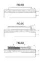
- FIG. 58 is a planar layout for explaining an integrated light emitting diode according to the second embodiment of the present invention.
- FIG. 59 is a schematic cross-sectional view for explaining an integrated light emitting diode according to the second embodiment of the present invention.
- FIGS. 60 through 65 are schematic cross-sectional views for explaining the fabricating process of an integrated light emitting diode according to the second embodiment of the present invention.
- FIGS. 66 through 68 are schematic cross-sectional views for explaining an integrated structure of a light emitting device, a waveguide, and a light receiving element according to the second embodiment of the present invention.
- FIG. 69 is a schematic cross-sectional view for explaining the structure of an integrated light emitting diode according to the third embodiment of the present invention.
- FIG. 70 is a planar layout for explaining the structure of an integrated light emitting diode according to the third embodiment of the present invention.
- FIGS. 71 through 81 are schematic cross-sectional view for explaining the fabricating process of an integrated light emitting diode according to the third embodiment of the present invention.
- FIG. 82 is a planar layout for explaining the structure of an integrated light emitting diode according to the third embodiment of the present invention.
- FIG. 83 is a schematic cross-sectional view for explaining an integrated light emitting diode and a waveguide according to the fourth embodiment of the present invention.
- FIG. 84 is a planar layout for explaining an integrated light emitting diode and a waveguide according to the fourth embodiment of the present invention.
- FIG. 85 is a schematic cross-sectional view for explaining an integrated light emitting diode, a waveguide, and a light receiving element according to the fourth embodiment of the present invention.
- FIGS. 86 through 93 are schematic cross-sectional views for explaining an integrated light emitting diode and a waveguide according to the fifth embodiment of the present invention.
- FIGS. 94 and 95 are schematic cross-sectional views for explaining an integrated structure of an integrated light emitting diode, a waveguide and CMOS according to the sixth embodiment of the present invention.
- FIGS. 96 through 111 are schematic cross-sectional views for explaining the fabricating method of an integrated structure of an integrated light emitting diode, a waveguide and CMOS according to the seventh embodiment of the present invention.
- FIG. 11 is a planar layout for an integrated light emitting diode according to the present invention
- FIG. 12 is a planar layout for a light receiving element according to the present invention
- FIGS. 13 through 18 are schematic cross-sectional views for stepwisely explaining the fabricating process of the integrated light emitting diode.
- a cross-sectional view taken along line A-A′ of the planar layout ( FIG. 11 ) is shown on the left hand side
- a cross-sectional view taken along line B-B′ of the planar layout ( FIG. 11 ) is shown on the right hand side.
- a 1 ⁇ m thick silicon oxide film 1900 is formed on a silicon support substrate 1100 and an SOI wafer having a 100 nm thick single crystalline silicon layer 1120 is thermally oxidized on the silicon oxide film, to form a 20 nm oxide film ( FIG. 13 ).
- a silicon thin film formation region (fin) and a contact region are formed ( FIG. 14 ) by using an active region pattern 1150 shown in FIG. 11 .
- a thin film-shaped, single crystalline region formed in perpendicular to the substrate is called a fin.
- a silicon surface exposed towards the side of the fin is thermally oxidized ( 1920 ) to set the silicon width formed by the fin to a predetermined thickness (5 nm).
- a resist mask 1800 is formed by a hole pattern 1850 of FIG. 11 , and arsenic is doped by ion implantation method with energy 25 keV and 2 ⁇ 10 15 cm ⁇ 3 to form an N-type impurity diffusion layer 1200 ( FIG. 16 ).
- a resist mask formed by inverting the pattern 1850 is formed, and boron is doped by ion implantation method with energy 5 keV and 2 ⁇ 10 15 cm ⁇ 3 to form a P-type impurity diffusion layer 1300 . In this way, a diode having a PN junction is formed.
- a P-N distance may be adjusted to form an i-region between P and N wells, instead of using the inverted mask as in this embodiment.
- a 300 nm silicon nitride film is deposited by CVD method, and a waveguide 1500 is processed by using a waveguide pattern 1550 of FIG. 11 .
- parallely arranged fins are coated with the waveguide 1500 .
- the term ‘waveguide’ is not limited to a single wavelength, but used as a light path in a broad sense (FIG. 17 ).
- a contact hole 1650 ( FIG. 11 ) is formed in the oxide film 1910 to form a metal wiring 1600 (not shown in FIG. 11 ).
- a forward bias can be applied to the PN junction. This enables to obtain the luminescence at a junction inside the parallely arranged fins. In case of arranging a plurality of fins, they are spaced away from each other by a half wavelength to more effectively increase luminescence. Moreover, this structure may be covered with a reflection film (to be described) for laser oscillation.
- the waveguide was put in the air, and a difference in refractive index between the silicon nitride film and the air was utilized to be able to confine light in the waveguide.
- a widely used method in ULSI is sealing a multilayer metal wiring or a chip in a package.
- a method shown in FIG. 19 and FIG. 110 may be used.
- FIG. 24 shows the results obtained in the process of FIG. 17 .
- a silicon oxide film 1930 is deposited to 1 ⁇ m and polishing by CMP is carried out to planarize it.
- the silicon oxide film having a relatively lower refractive index than the nitride film can act as a reflection coating.
- a contact hole is perforated into a corresponding oxide film to form a metal wiring 1600 . In this manner, an integrated light emitting diode and a waveguide compatible with the prior art ULSI may be formed.
- FIGS. 21 and 22 show other waveguide connecting configurations.
- the silicon oxide film 1910 is removed by wet etching in hydrofluoric acid and the BOX 1900 is etched at the same time to remove an oxide film below the fins.
- the fin section is separated from the oxide film as shown in the drawing on the right hand side ( FIG. 21 ).
- the silicon nitride film is deposited to cover the entire fin section with the waveguide 1500 ( FIG. 22 ).
- FIG. 12 shows a planar layout of the light receiving element.
- FIGS. 23 through 26 show the fabricating process in reference to its cross-sectional structure. Because the light emitting diode explained earlier and the light receiving element being explained here are integrated on the same wafer, they are originally formed at the same time. They are separately described for convenience in explaining the structure of the integrated light emitting diode.
- a P-type doped SOI layer 1120 is processed by using an active region pattern 1160 of FIG. 12 . This process ( FIG. 23 ) corresponds to the SOI layer processing illustrated in FIG. 14 .
- reference numerals of corresponding processes will be referred in the following description.
- An N-type diffusion region 1210 is formed by using a pattern 1860 in FIG. 12 .
- a P-type high concentration impurity region 1310 is formed ( FIG. 24 ).
- a silicon nitride film 1500 waveguide is formed (see FIG. 25 and FIG. 17 ).
- a light receiving element is obtained by forming a metal wiring on an electrode layer (see FIG. 26 and FIG. 20 ).
- a PN diode of the light receiving element can be arranged in a horizontal direction ( FIG. 27 ). Meanwhile, if the PN diode is arranged in a vertical direction, an electric field region by the PN junction can be great whereas the width of the electric field by the PN junction is limited depending on the film thickness of the SOI layer.
- the structure using the SOI wafer explained here is characterized by having a sufficiently thick BOX 1900 . Therefore, this oxide film may be utilized even for the formation of the waveguide 1500 .
- the BOX 1900 is processed concurrently with the processing of the waveguide 1500 to obtain a convex shape.
- a silicon oxide film 1960 , a silicon nitride film 1961 , a silicon oxide film 1962 , and a silicon nitride film 1963 are laminated by CVD to form a high reflection film (HR film), and a clad having the waveguide 1500 as a core layer is formed ( FIG. 29 ). In this way, it becomes possible to trap light in the waveguide 1500 more efficiently.
- a well-known HR formation method can also be utilized, wherein the film thickness of a laminate forming the HR is set to 1 ⁇ 4 of the wavelength.
- the film thickness of the laminate becomes about 100-200 nm for the silicon nitride film and the silicon oxide film because of refractive index. Since this is done in similar order to the interlayer insulation film used for a prior art LSI wiring process, it is rather convenient to apply the prior art formation process.
- stacking a laminate with different refractive index for increasing the reflection efficiency can be done repeatedly without difficulty.
- FIG. 30 shows a planar layout of an exemplary withdrawal portion
- FIGS. 31 through 41 stepwisely show the fabricating process in reference to the cross-sectional structures taken along lines A-A′, B-B′, and C-C′ in FIG. 30 .
- FIG. 31 shows the formation of a nitride film plug, wherein a light emitting element is formed, and the silicon oxide film 1930 is deposited, planarized by CMP, and perforated by a waveguide withdrawal pattern 1560 of FIG. 30 . Finally, the silicon nitride film 1510 is deposited and etched back. It is also possible to utilize the CMP method instead of an etch back technique for this process.
- the silicon nitride film functioning as a waveguide is deposited by CVD, and a resist pattern 1700 of FIG. 32 is formed by using 1750 shown in FIG. 30 .
- a nitride film 1500 is then dry etched by using the resist pattern. At this time, etching conditions are selected to create a deposition atmosphere for the reaction product, to thereby make the processed side in an inclined form ( FIG. 33 ).
- a resist 1555 is formed ( FIG. 34 ) by the waveguide pattern 1550 of FIG. 30 .
- the silicon nitride film 1500 is processed by using the resist 1555 as a mask ( FIG. 35 ).
- the high reflection film 1970 which is a laminate of the silicon oxide film and the silicon nitride film is deposited to cover the waveguide 1500 .
- the silicon oxide film and the silicon nitride film have refractive index of about 1.5 and 2, respectively.
- SiON silicon oxy-nitride
- a horizontal waveguide 1500 placed over the vertical waveguide 1510 and the oxide film 1930 is connected at an angle, i.e., with a 45-degree reflective plane.
- a light that is propagated in the normal direction from the integrated light emitting diode to the substrate plane can travel in a different direction, such as, in the direction parallel to the substrate plane.
- this embodiment illustrated the connection from the integrated light emitting diode the same structure may also be formed in the light receiving element section.
- This waveguide formation process is characterized in that it can adopt the ULSI wiring process as it is.
- FIG. 37 diagrammatically shows a ULSI wiring with a wide metal multilayer wire.
- the drawing also shows an integrated light emitting diode 1400 and a light receiving element 1410 formed on the BOX 1900 , respectively.
- As an example of a multi-layer wire three metal layers 1600 , 1601 , and 1603 are shown.
- Each of the interlayer insulation films is denoted by reference numerals 1930 , 1931 , and 1932 . Insulation films of the silicon oxide and silicon nitride are used as materials for the waveguide formation process, and they are actually major ingredients during the wiring process up to now.
- the vertical waveguide 1510 is formed, similar to the formation of a contact in the metal wiring. This is repeated for every layer of the multi-layer wiring to form a vertical direction waveguide. Needless to say, this can be performed separately from the formation of contact in the metal wiring.
- the hole as in the vertical waveguide can be perforated en bloc after the formation of double or multi-layer interlayer film. Because the laminate high reflection layer 1970 can also function as an interlayer insulation film, as shown in the drawing, the metal wiring 1602 can be put on the clad 1970 .
- FIG. 38 illustrates a case where a waveguide is formed below the metal wiring.
- 1600 denotes a metal plug layer
- 1601 is a metal wiring layer formed by a so-called damascene process.
- the metal wiring layer is not yet formed.
- a high-temperature deposition technique can be applied to deposit the silicon nitride film used as a waveguide, and the refractive index is easily set.
- FIGS. 39 through 42 stepwisely show the formation of a structure where a waveguide is covered with a high reflection film.
- An integrated light emitting diode 1400 and a light receiving element 1410 are formed, and a laminate high reflection film 1971 combining an insulating film 1930 , a silicon oxide film, and a silicon nitride film ( FIG. 39 ) is formed.
- a vertical waveguide 1510 is formed ( FIG. 40 ).
- FIG. 41 a clad 1970 having the waveguide 1500 as a core layer is formed ( FIG. 41 ).
- FIG. 47 depicts the formation of the metal wiring 1600 in each diode. As the entire area can be covered by the high reflection films 1970 and 1971 , it becomes possible to trap light in the waveguide 1500 more efficiently.
- FIG. 43 shows an exemplary planar layout
- FIGS. 45 through 60 stepwisely show the fabricating process by using cross-sectional views (A-A′ cross section of FIG. 43 ).
- This method is based on a dummy pattern 1152 , but the dummy pattern can be arranged in two different forms, i.e., a convex pattern or a hole pattern.
- FIG. 43 shows a convex pattern
- FIG. 44 shows a hole pattern. According to the fabricating process of this embodiment, after the dummy pattern 1152 of FIG. 43 and FIG.
- fins are self-aligned with respect to the dummy pattern.
- spacers 1202 , 1203 , 1204 , 1205 , 1981 , 1982 , and 1983 used for fin formation are not necessarily found in a photo mask, but they are indicated at pattern positions of the layout after the formation in order to show the arrangement relation.
- a 300 nm silicon nitride film is deposited on a 50 nm thick SOI 1201 , and a convex shape pattern is formed by the hole pattern 1152 shown in FIG. 43 .
- the convex shape looks like a projected shape 1102 formed on the plane in the cross-sectional view.
- a concave shape is formed instead of the convex shape.
- an amorphous silicon 1202 is deposited to a thickness of 10 nm and heated to be crystallized. Because crystal growth occurs in a seed layer of single crystalline silicon 1201 , single crystals 1201 having crystal orientation are obtained below the side of the projected shape 1102 . In this manner, fins are produced.
- the silicon surface may be thermally oxidized to adjust the film thickness of the fin to a predetermined thickness.
- the silicon nitride film 1981 is deposited to a thickness of 20 nm and etched by anisotropic dry etching by the deposition thickness to form the silicon nitride film 1981 in side wall spacer shape.
- FIG. 47 the process explained above is repeated to obtain a laminate structure consisting of thin, amorphous silicon layers 1203 , 1204 , and 1205 and the nitride film spacers 1982 and 1983 .
- a photoresist hole pattern is formed by using the pattern 1165 shown in FIG. 43 to etch the laminate film of the silicon nitride film and the silicon thin film and expose the BOX 1900 (not shown).
- the silicon nitride film 1500 is then deposited to a thickness of 500 nm to cover the integrated light emitting diode.
- the deposited nitride film by CMP is planarized to expose a dummy 1102 .
- the pattern 1150 shown in FIG. 43 as a mask, an N-type region is formed below the fin and on the plane 1300 and a P-type region 1200 is formed on the upper portion by ion implantation, so that a PN junction is formed inside the fin in the vertical direction.
- a polycrystalline silicon 1240 doped with a P-type high concentration impurity is deposited to a thickness of 50 nm and processed with the pattern 1855 shown in FIG. 43 .
- the silicon nitride film 1500 is processed by using the waveguide pattern 1550 to form a waveguide.
- the processing in use of the pattern 1165 which was explained in reference to FIG. 53 and the formation of the waveguide 1500 can be carried out at the same time. That is, a hole is formed by the pattern 1165 shown in FIG. 44 and the silicon nitride film 1500 is deposited by CMP, to obtain a silicon nitride film waveguide of the hole pattern 1165 . In this manner, the formation of the silicon nitride film 1500 having been discussed in FIG. 51 may be omitted.
- the silicon oxide film as an interlayer film is deposited and planarized, followed by performing the metal wiring on each electrode.
- the same spacer process can be used to form fins on the SOI substrate by etching.
- the surface of the SOI substrate 1120 is thermally oxidized to form an oxide film 1905 with a thickness of 20 nm.
- a dummy pattern 1103 is formed by polycrystalline silicon, and the silicon nitride film 1985 and the polycrystalline silicon 1206 are alternately deposited to produce a thick nitride film 1986 .
- a convex region is planarized by CMP to expose an upper portion of the dummy pattern 1103 .
- the nitride film is etched by wet etching, and a polycrystalline silicon pattern is formed.
- a target mask is etched anisotropically and transferred as a pattern to the oxide film 1905 .
- the SOI silicon layer is etched by using the oxide film pattern as a mask to obtain a fin pattern.
- This fin pattern is preferably used to form a light emitting diode.
- a minute fin pattern was obtained by the laminate film.
- a mask pattern may be obtained to form fins by the spacer process.
- fins were used primarily for forming an integrated light emitting diode, but the integrated light emitting diode can also be obtained by laminating the silicon thin film in parallel to the substrate plane.
- FIG. 58 shows a planar layout
- FIG. 59 is a cross-sectional view taken along line B-B′ of FIG. 58 .
- the following will explain the fabricating process, referring to FIGS. 60 through 65 which are A-A′ cross sections of FIG. 58 .
- a 10 nm silicon germanium film 1121 and a 10 nm silicon layer 1120 are epitaxially grown in turn on the SOI substrate 1120 by MBE technique.
- a laminate film 1155 is etched by using an active region pattern 1150 of FIG. 58 .
- a PN junction is formed by using an ion implantation mask 1850 and its inversed pattern shown in FIG. 58 .
- the silicon germanium crystalline layer is selectively etched by using a thin mask pattern 1165 of FIG. 58 , to obtain a hollow shaped thin film structure of the silicon thin film having the PN junction.
- the silicon nitride film is deposited and processed by using the waveguide pattern 1550 ( FIG. 58 ).
- the hollow shaped region that is formed with the silicon thin film has a buried structure by the silicon nitride film.
- an interlayer insulation film and a metal wiring are formed to obtain an integrated light emitting diode that integrates a thin film in the vertical direction.
- the integrated light emitting diode 1400 and the light receiving element 1410 are formed on two wafers, respectively, and a waveguide 1510 is formed. While the waveguide 1510 being exposed, a low reflection film (AR film) 1990 is formed by laminating the silicon oxide film and the silicon nitride film, and both wafers with the AR film interposed therebetween may be joined for waveguide connection.
- AR film low reflection film
- a support base plate of SOI is removed and layers are laminated to obtain a multi-layer structure.
- the AR film may be inserted in the junction interface.
- the outer circumference of the waveguide 1500 is covered with the HR film 1970 and the AR film 1990 is placed at the junction. This structure makes it possible to realize high propagation efficiency of light.
- This embodiment discloses a luminous region expansion method that does not require a laminate film or plural wall-type silicon thin films disclosed in Embodiment 1 and Embodiment 2.
- silicon semiconductor regions 3303 and 3304 of different conductive types are arranged adjacent each other on a silicon oxide film 3302 formed on the surface of the silicon substrate 3301 , and a silicon oxide film 3305 is formed in the periphery of the interface of these two semiconductor regions only in such a manner that it covers a portion of the surfaces of the two semiconductor regions.
- a silicide 3306 the compound of silicon and a metal, is formed on the surface of a semiconductor region that is not covered with the silicon oxide film 3305 .
- a part of the silicon substrate 3301 that is, the silicon substrate in a region having the light emitting diode formed thereon, is removed to expose the silicon oxide film 3302 , and a metal layer 3307 functioning as a light reflection film is deposited thereon.
- FIG. 70 shows a planar structure of the light emitting diode of this embodiment 3, where 3301 and 3302 denote a silicon substrate and a silicon oxide film formed thereon, respectively. What is on the top surface is the silicon oxide film 3302 .
- 3304 denotes a conductive type semiconductor region on one side
- 3303 denotes a conductive type semiconductor region on the other side
- 3305 denotes a silicon oxide region formed in a manner to cover the two conductive type semiconductor regions. Therefore, the light emitting diode of this embodiment is characterized by its planar structure where the circumference of one conductive type silicon semiconductor region is covered by the other conductive type semiconductor region. The junctions in the circumference become luminous regions.
- the luminous area can be expanded simply by increasing the number of junctions as much as desired.
- the semiconductor region whose circumference is covered may be laid out in a narrow and long shape instead of a circular shape or a rectangle shape close to a square, so that the length of the luminous PN junction can be increased relatively larger than the layout area.
- Another characteristic of the light emitting diode of this embodiment is that all the junctions are formed inside the semiconductor regions, and its edges never stick out of the ends of the semiconductor region. Therefore, leak current caused by the edges does not occur.
- Still another characteristic of the light emitting diode of this embodiment is that the surfaces of the two conductive type semiconductor regions not being covered with the silicon oxide film 3305 are covered with the silicide film. The light generated by this silicide film can easily and efficiently get out through the silicon oxide film 3305 acting like a window. Furthermore, in presence of silicide, uniform voltage can be applied and a stable operation can be realized.
- a silicon oxide film 3302 is grown on a surface of the silicon substrate to a thickness of 100-200 nm by a prior art heat oxidation method or the like. Then, a single crystalline silicon film 3310 is laminated on a surface of the oxide film by using a well-known laminating technique.
- This is a so-called Silicon On Insulator (SOI) structure, which is a kind of silicon substrates used broadly as a part of a semiconductor product such as a high performance micro processor, etc.
- SOI Silicon On Insulator
- This embodiment also employs the SOI substrate purchased from a wafer manufacturer, provided that the SOI substrate has plane orientation 100 and is about 50 nm thick.
- the silicon thin film 3310 on the oxide film is processed in a desired shape, a convex shape for example ( FIG. 72 ).
- the size of the silicon thin film 3310 varies depending on the size of a region formed therein and the size of a luminous region.
- a photoresist pattern 3311 to function as an ion implantation mask is first formed by lithography as depicted in FIG. 73 , and only an impurity implanted region is perforated.
- arsenic or phosphor is implanted with a dose of 10 14 -10 15 /cm 2 through this opening or hole.
- a photoresist pattern used as an ion implantation mask is removed by cleansing. Thereafter, a photoresist pattern 3312 is formed by lithography to cover an already implanted impurity region. Then, boron ions are implanted with a dose of 10 14 -10 15 /cm 2 by using the photoresist pattern as a mask.
- the photoresist pattern is removed by cleansing and heated to activate impurities.
- an N-type semiconductor region 3303 with plenty of electrons and a P-type semiconductor region 3304 with plenty of holes are formed.
- the heating treatment was performed at 900° C.
- a silicon nitride film 3313 for covering a surface of the substrate is processed by lithography and dry etching to expose the surface of the silicon thin film in the periphery of the interface between the N-type semiconductor region 3303 and the P-type semiconductor region 3304 .
- the entire substrate is placed under a high-temperature oxidation atmosphere, so that a silicon oxide film 3305 may selectively grow only on a portion of the surface of the N-type and the P-type semiconductor region not being covered with the silicon nitride film 3313 .
- This technique is called a selective oxidation of silicon and has already been used by many.
- the oxidation atmosphere contains hot steam of 1000° C.
- This hot steam oxidation atmosphere unlike the oxygen atmosphere, helps a relatively thick oxide film to grow within a short amount of time.
- the grown oxide film is about 80 nm thick, so a silicon region (this includes an interface between the N-type and the P-type) of about 10 nm in thickness is formed on the partially oxidized silicon thin film.
- the silicon nitride film 3313 that became a selected oxidation mask during the process shown in FIG. 77 is selectively removed.
- the substrate is impregnated in a hot phosphoric acid solution. It turned out, as shown in FIG. 78 , a semiconductor region is exposed while leaving the grown oxide film.
- a metal such as titan, cobalt, nickel and so on is deposited on the entire surface to a thickness of several tens of nanometers and heated at 450° C. under nitrogen atmosphere to remove, by using a hydrogen peroxide containing solution, nonreacted metals that are deposited on the oxide film 3305 .
- the metal deposited on the silicon thin film causes a chemical reaction under heating and is silicided, so it is not to be removed by a solution. In this manner, a silicide-free structure is formed on the oxide film 3305 , as shown in FIG. 79 .
- an additional heating operation at 700° C. needs to be performed to lower the resistance of silicide. This technique is already customarily used in the silicon semiconductor process.
- a metal layer used as a light reflection plate is formed by deposition to complete the fabrication of a light emitting diode. Even though only the fabricating method of a light emitting diode has been explained in this embodiment, it is actually incorporated with the fabricating method of a peripheral semiconductor device or the process for electrically and optically connecting such a semiconductor device with a light emitting diode. Because of this, the metal layer functioning as a reflection plate is adhered to a back surface of the substrate customarily at the end of the process. In case of including a wiring process, a wiring via which current flows into the two semiconductor regions in the light emitting region and a contact hole are formed, as shown in FIG. 82 .
- a waveguide for guiding light emitted by the light emitting diode to the light receiving element is mounted.
- Light emitted by the light emitting diode shows the highest luminescence intensity around 1000 nm wavelength, which is because light emission has occurred as a result of recrystallization due to the band gap of ultra-thin silicon.
- the light emitting diode 3318 is fully covered with a silicon nitride film 3317 and the silicon nitride film 3317 is arranged in a waveguide pattern on the substrate, similarly to the state shown in FIG. 84 , and a light receiving element 3319 is arranged at the end thereof.
- FIG. 85 is a cross-sectional view of a chip comprising a group of elements that consists of a light emitting diode 3318 , a light receiving element 3319 , and a silicon nitride film 3317 being integrated together.
- a typical light receiving element made out of silicon is used for the light receiving element 3319 .
- the light receiving element is prepared in use of a single crystalline silicon thin film formed over the oxide film on the surface of the substrate 3301 and formed concurrently with others by the prior art silicon semiconductor process.
- This embodiment is related to a waveguide for efficiently propagating light.
- a silicon oxide film 3320 is deposited as an interlayer insulation film in a manner that it covers the entire light emitting diode 3318 and then planarized by the prior art CMP.
- a waveguide 3321 is arranged right above the periphery of two conductive interfaces (a luminous region).
- the waveguide is made out of a silicon nitride film and traps light therein. Therefore, the nitride film waveguide 3321 is inevitably covered with a silicon oxide film for example having a small dielectric constant. In the interest of brevity, this is not going to be explained in further detail.
- the cross section of the waveguide is almost semicircular.
- the end portion of the waveguide where the light emitting diode and the light receiving element is arranged has a shape of a quarter of a sphere. Therefore, light from the light emitting diode is reflected from the end at high rate to propagate the waveguide.
- the other end portion of the waveguide has also a shape of a quarter of a sphere, the light having propagated the waveguide is now reflected from the end of the waveguide and directed nearly perpendicularly to the light receiving element. Further details on the effects of a waveguide configuration of this shape are provided in U.S. Pat. No. 6,868,214B1.
- a cross section without a luminous region is going to be used as an example.
- a silicon nitride film 3321 is deposited on a surface of the interlayer insulation film 3320 .
- the nitride film is processed in a rectangular shape by lithography or dry etching of the prior art. Since the silicon nitride film and the silicon oxide film functioning as an interlayer insulation film are dry etched at different speeds, the processing of the nitride film may be interrupted with the oxide film.
- the silicon nitride film is deposited by CVD so that a film of even thickness can be deposited over the surface of the rectangular silicon nitride film as well as the surface of the interlayer insulation film.
- a side wall film 3322 with a circumference drawing an arc only on the side walls of the rectangular silicon nitride film 3321 is formed.
- this side wall film although it is difficult to make the cross section of the waveguide have a perfect hemisphere shape, the anisotropic dry etching method being frequently used in the silicon semiconductor process and the silicon nitride film may be utilized to form side wall films as desired. This approach is actually known to be highly compatible with a silicon semiconductor.
- the side wall film formation is preferably repeated several times to get a more hemispherical shaped cross section.
- Another method is to make a waveguide out of glass having a relatively low melting point.
- the waveguide has to be made of a material that has a greater refractive index than the silicon oxide film functioning as an interlayer insulation film and that is capable of sustaining heat treatment (about 500° C.) in the following wiring process.
- glass 3323 is applied to the surface of the interlayer insulation film 3320 as shown in FIG. 91 and processed with the rectangular waveguide pattern as shown in FIG. 92 , by dry etching of the prior art. And, this is heated at about 600° C. and fluidified to form a waveguide having a hemisphere cross section as illustrated in FIG. 93 .
- a light emitting diode of this embodiment is easily fabricated by using a silicon thin film, so it can be mixed with a semiconductor element having a silicon substrate, e.g., Metal Oxide Semiconductor Field Effect Transistor (MOSFET), etc.
- FIG. 94 illustrates a case that both of a light emitting diode and a semiconductor element (a switching element configured with CMOS: nMOSFET and pMOSFET) are formed on a single crystalline silicon thin film on a silicon oxide film 3302 over a substrate. That is, it is the MOSFET with the SOI structure.
- 3324 denotes a first conductor type silicon thin film
- 3325 denotes a second conductor type silicon thin film
- 3326 denotes an element isolation oxide film that is a silicon oxide for performing electrical insulation-separation of two MOSFETs
- 3327 denotes a gate oxide film of MOSFET
- 3328 denotes a gate electrode of MOSFET
- 3329 denotes a second conductive type semiconductor region
- 3330 denotes a first conductive type semiconductor region
- 3331 denotes a buried metal called a plug for electric connection between a wiring and a semiconductor element
- 3332 denotes a wiring metal.
- FIG. 95 depicts a MOSFET formed over a silicon substrate.
- a single crystalline silicon film formed on an oxide film 3302 over the substrate and the oxide film 3302 are removed to expose the surface of the silicon substrate.
- this silicon substrate is employed to form a MOSFET.
- the oxide film 3302 has a thickness of 100-200 nm
- a stepped difference due to an oxide film is produced between the silicon thin film used for a light emitting diode and the substrate for MOSFET applications. Therefore, according to this embodiment, a silicon was selectively epitaxially grown on the exposed silicon surface and a single crystalline silicon layer having a thickness of 100-200 nm was grown. In consequence, the stepped difference was substantially reduced and the light emitting diode and the semiconductor device could be fabricated at the same time.
- FIG. 96 and subsequent drawings describe a method for integrating a light emitting diode with an electric device such as MOSFET at the same time.
- the example shown in FIG. 96 used a SOI substrate having a single crystalline silicon film 3310 formed over a silicon oxide film 3302 .
- silicon substrates without a BOX 3302 in one portion may be used instead as shown in FIG. 95 .
- an element isolation oxide film 3326 is formed for electrical insulation-separation of elements.
- any of the prior art silicon microscopic processing techniques such as silicon hole processing, silicon oxidation, silicon oxide burial, polishing, etc., can be employed.
- FIG. 97 illustrates a case that a luminous region forming area (the single crystalline silicon region on the left side), a first conductive type MOSFET forming area (the single crystalline silicon region at the center), and a second conductive type MOSFET forming area (the single crystalline silicon region on the right side) are formed.
- a light emitting diode is fabricated.
- a first conductive type region 3304 is formed by ion implantation of the prior art, and a second conductive type region 3303 is formed inside the first conductive type region by ion implantation as well.
- arsenic ions were implanted in the first conductive type region 3304 with a dose of 10 15 /cm 2
- boron ions were implanted in the second conductive type region 3303 with a dose of about 10 15 /cm 2 .
- a region 3324 used as a base plate for the first conductive type MOSFET is prepared by ion implantation, and a region 3325 used as a base plate for the second conductive type MOSFET is also prepared by ion implantation.
- phosphor ions were implanted in the base plate area 3324 for the first conductive type MOSFET with a dose of about 10 13 /cm 2
- boron ions were implanted in the base plate area 3325 for the second conductive type MOSFET with a dose of about 10 13 /cm 2 .
- silicon oxidation is carried out to reduce the thickness of a silicon film in the proximity of the interface between the first and the third conductive type luminous areas.
- silicon oxidation is carried out to reduce the thickness of a silicon film in the proximity of the interface between the first and the third conductive type luminous areas.
- an oxidized area deposits an apertured silicon nitride film 3313 ( FIG. 100 ). It is placed in an oxidation kiln containing hot moisture of about 1000° C. to oxidize the silicon thin film by about 40 nm only. Then, an oxide film with a thickness of about 80 nm grows and a single crystalline silicon region with a thickness of about 10 nm remains ( FIG. 101 ).
- MOSFET MOSFET
- a gate oxide film 3327 of MOSFET is grown by silicon oxidation technique of the prior art.
- the film thickness was set to about 2 nm.
- polycrystalline silicon is first deposited to a thickness of about 250 nm on the entire surface of the substrate to form the gate electrode of MOSFET. It is processed in the MOSFET's gate electrode shape 3328 as shown in FIG. 103 .
- the processed size is about 90 nm. At this time, it is important that the processing of the gate electrode stops on a thin gate oxide film (i.e., 2 nm).
- impurities of a different conductive type from the substrate are implanted by using each gate electrode 3328 as a mask.
- the substrate contains phosphor
- boron ions are implanted in the diffusion layer in a dose of about 10 15 /cm 2 .
- the substrate includes boron
- phosphor or arsenic is implanted in the diffusion layer in a dose of about 10 15 /cm 2 .
- Each impurity is implanted in the gate electrode, and low resistivity and work function of the gate electrode are determined thereby.
- a side wall insulation film is formed only on the side walls of the gate electrode as shown in FIG. 105 , as a step prior to silicidation of areas in the diffusion layer, gate electrode and light emitting diode, which the areas are not covered by an oxide film.
- a silicon oxide film or a silicon nitride film is first deposited on the entire surface of the substrate by CVD of the prior art.
- anisotropic dry etching is carried out, a side wall insulation film 3333 remains only on the side walls of the rectangular gate electrode as shown in FIG. 105 .
- a 20-30 nm thick metal selected from titan, cobalt, nickel, etc. is deposited thereon. And, a heat treatment at around 450° C. is carried out to cause a reaction between silicon and the metal, thereby producing a metal silicate (silicide) 3306 .
- the silicide is formed only on the exposed silicon surface, and not formed on the side walls of the gate electrode coated with the side wall insulation film 3333 , or on the silicon oxide covering a luminous region in a light emitting diode. Therefore, these areas remain in metal state.
- silicide is eventually formed only on an interface with silicon as shown in FIG. 106 .
- an additional heating treatment at about 750° C. needs to be performed to lower the resistance of silicide. Accordingly, the resistance of the gate electrode and the resistance of the diffusion layer are lowered, while the MOSFET and the light emitting diode is driven at low voltage.
- an interlayer insulation film 3334 is deposited in a manner that it covers the light emitting diode and the MOSFET.
- the interlayer insulation film 3334 is then polished and planarized.
- an optical waveguide 3321 is fabricated at an upper portion of a luminous region, as explained before. And, the waveguide is covered with an insulation film having a refractive index smaller than the waveguide, and is planarized.
- a wiring, a diffusion layer or a gate electrode of MOSFET, and a metal plug for connecting the silicon region of the limit emitting diode are sequentially formed.
- the metal plug is formed by perforating a contact hole in the interlayer film, filling the contact hole with metals, and scraping by polishing the metal film adhered onto the surface of the interlayer insulation film.
- the wiring is performed in use of aluminum for example, and an aperture (or opening) is formed into a support base substrate of the light emitting section as shown in FIG. 111 .
- a metal layer functioning as a light reflection plate is formed to complete the fabrication of an opto-electronic integrated circuit (OEIC).
Abstract
Description
ψ(r)=φk
φk
[ε(k 0 −i∇)+V(r)]ξ(r)=Eξ(r)
ψ(r)=√{square root over (2)}u k
ψ(r)=√{square root over (2)}u k
Claims (13)
Applications Claiming Priority (2)
| Application Number | Priority Date | Filing Date | Title |
|---|---|---|---|
| JP2007-036328 | 2007-02-16 | ||
| JP2007036328A JP4996938B2 (en) | 2007-02-16 | 2007-02-16 | Semiconductor light emitting device |
Publications (2)
| Publication Number | Publication Date |
|---|---|
| US20080197362A1 US20080197362A1 (en) | 2008-08-21 |
| US8030668B2 true US8030668B2 (en) | 2011-10-04 |
Family
ID=39420503
Family Applications (1)
| Application Number | Title | Priority Date | Filing Date |
|---|---|---|---|
| US11/935,904 Expired - Fee Related US8030668B2 (en) | 2007-02-16 | 2007-11-06 | Semiconductor LED, opto-electronic integrated circuits (OEIC), and method of fabricating OEIC |
Country Status (4)
| Country | Link |
|---|---|
| US (1) | US8030668B2 (en) |
| EP (1) | EP1959504A3 (en) |
| JP (1) | JP4996938B2 (en) |
| KR (1) | KR20080076694A (en) |
Cited By (8)
| Publication number | Priority date | Publication date | Assignee | Title |
|---|---|---|---|---|
| US20170068047A1 (en) * | 2015-09-04 | 2017-03-09 | Renesas Electronics Corporation | Semiconductor device and method for manufacturing the same |
| US9864138B2 (en) | 2015-01-05 | 2018-01-09 | The Research Foundation For The State University Of New York | Integrated photonics including germanium |
| US10698156B2 (en) | 2017-04-27 | 2020-06-30 | The Research Foundation For The State University Of New York | Wafer scale bonded active photonics interposer |
| US10816724B2 (en) | 2018-04-05 | 2020-10-27 | The Research Foundation For The State University Of New York | Fabricating photonics structure light signal transmission regions |
| US10877300B2 (en) | 2018-04-04 | 2020-12-29 | The Research Foundation For The State University Of New York | Heterogeneous structure on an integrated photonics platform |
| US10976491B2 (en) | 2016-11-23 | 2021-04-13 | The Research Foundation For The State University Of New York | Photonics interposer optoelectronics |
| US11029466B2 (en) | 2018-11-21 | 2021-06-08 | The Research Foundation For The State University Of New York | Photonics structure with integrated laser |
| US11550099B2 (en) | 2018-11-21 | 2023-01-10 | The Research Foundation For The State University Of New York | Photonics optoelectrical system |
Families Citing this family (27)
| Publication number | Priority date | Publication date | Assignee | Title |
|---|---|---|---|---|
| JP5003013B2 (en) * | 2006-04-25 | 2012-08-15 | 株式会社日立製作所 | Silicon light-emitting diode, silicon phototransistor, silicon laser, and manufacturing method thereof. |
| JP5117156B2 (en) * | 2007-10-05 | 2013-01-09 | 株式会社日立製作所 | Semiconductor device |
| FR2925728B1 (en) * | 2007-12-20 | 2010-01-01 | Commissariat Energie Atomique | METHOD FOR MANUFACTURING ORGANIC DIODE IDENTIFICATION AND AUTHENTICATION DEVICE, DEVICE AND METHOD OF USE |
| US20100289037A1 (en) * | 2008-01-15 | 2010-11-18 | Shin Matsumoto | Semiconductor device, manufacturing method thereof and display device |
| JP2010238722A (en) * | 2009-03-30 | 2010-10-21 | Hitachi Ltd | Silicon light-emitting element |
| US8269931B2 (en) * | 2009-09-14 | 2012-09-18 | The Aerospace Corporation | Systems and methods for preparing films using sequential ion implantation, and films formed using same |
| US8946864B2 (en) | 2011-03-16 | 2015-02-03 | The Aerospace Corporation | Systems and methods for preparing films comprising metal using sequential ion implantation, and films formed using same |
| JP5762851B2 (en) * | 2011-06-28 | 2015-08-12 | 株式会社日立製作所 | Silicon and germanium light emitting devices |
| US9209091B1 (en) | 2011-08-05 | 2015-12-08 | Maxim Integrated Products, Inc. | Integrated monolithic galvanic isolator |
| WO2013118248A1 (en) * | 2012-02-06 | 2013-08-15 | 株式会社日立製作所 | Light-emitting element |
| US8995800B2 (en) * | 2012-07-06 | 2015-03-31 | Teledyne Scientific & Imaging, Llc | Method of fabricating silicon waveguides with embedded active circuitry |
| US20140027808A1 (en) * | 2012-07-26 | 2014-01-30 | University Of Rochester | Lateral carrier injection infrared light emitting diode structure, method and applications |
| US20140103452A1 (en) | 2012-10-15 | 2014-04-17 | Marvell World Trade Ltd. | Isolation components for transistors formed on fin features of semiconductor substrates |
| JP2014093500A (en) * | 2012-11-07 | 2014-05-19 | Nippon Telegr & Teleph Corp <Ntt> | Light-emitting device |
| JP2014165292A (en) * | 2013-02-25 | 2014-09-08 | Hitachi Ltd | Light-emitting element, manufacturing method of the same and optical transmitter/receiver |
| US9324579B2 (en) | 2013-03-14 | 2016-04-26 | The Aerospace Corporation | Metal structures and methods of using same for transporting or gettering materials disposed within semiconductor substrates |
| US9690042B2 (en) | 2013-05-23 | 2017-06-27 | Electronics And Telecommunications Research Institute | Optical input/output device, optical electronic system including the same, and method of manufacturing the same |
| US9362444B1 (en) * | 2015-03-18 | 2016-06-07 | International Business Machines Corporation | Optoelectronics and CMOS integration on GOI substrate |
| KR101677542B1 (en) * | 2015-04-15 | 2016-11-18 | 연세대학교 산학협력단 | Flexible high performance inorganic matter FET using built-in strain of inorganic matter on Insulator wafer |
| JP6697858B2 (en) * | 2015-09-04 | 2020-05-27 | ルネサスエレクトロニクス株式会社 | Semiconductor device and manufacturing method thereof |
| WO2017155470A1 (en) * | 2016-03-09 | 2017-09-14 | Agency For Science, Technology And Research | Self-determining inspection method for automated optical wire bond inspection |
| US9653441B1 (en) * | 2016-06-20 | 2017-05-16 | International Business Machines Corporation | Monolithic integration of a III-V optoelectronic device, a filter and a driving circuit |
| EP3340403B1 (en) * | 2016-12-23 | 2023-06-28 | IMEC vzw | Improvements in or relating to laser devices |
| CN117148498A (en) | 2017-04-19 | 2023-12-01 | 卢克斯特拉有限公司 | Method and system for two-dimensional pattern matching grating coupler |
| FR3079036A1 (en) * | 2018-03-15 | 2019-09-20 | Stmicroelectronics (Crolles 2) Sas | FILTERING DEVICE IN A WAVEGUIDE |
| TWI683370B (en) * | 2019-03-12 | 2020-01-21 | 環球晶圓股份有限公司 | Semiconductor device and manufacturng method thereof |
| JP7467146B2 (en) | 2020-02-07 | 2024-04-15 | ソニーセミコンダクタソリューションズ株式会社 | Light-emitting device, method for manufacturing light-emitting device, and display device |
Citations (3)
| Publication number | Priority date | Publication date | Assignee | Title |
|---|---|---|---|---|
| US5466948A (en) * | 1994-10-11 | 1995-11-14 | John M. Baker | Monolithic silicon opto-coupler using enhanced silicon based LEDS |
| US6295390B1 (en) * | 1994-08-23 | 2001-09-25 | Canon Kabushiki Kaisha | Image input/output apparatus with light illumination device for two-dimensional illumination |
| US6868214B1 (en) | 1999-07-30 | 2005-03-15 | Canon Kabushiki Kaisha | Optical waveguide, method of fabricating the waveguide, and optical interconnection device using the waveguide |
Family Cites Families (9)
| Publication number | Priority date | Publication date | Assignee | Title |
|---|---|---|---|---|
| JP3181303B2 (en) * | 1990-04-20 | 2001-07-03 | 株式会社日立製作所 | Light emitting element |
| JPH06140669A (en) * | 1992-10-29 | 1994-05-20 | Hitachi Ltd | Light emitting element and manufacture thereof |
| JPH06268254A (en) * | 1993-03-15 | 1994-09-22 | Toshiba Corp | Semiconductor device |
| JPH0846237A (en) * | 1994-07-27 | 1996-02-16 | Nippon Telegr & Teleph Corp <Ntt> | Silicon light-emitting diode |
| JPH09205223A (en) * | 1995-11-24 | 1997-08-05 | Denso Corp | Semiconductor device |
| JPH10144953A (en) * | 1996-11-05 | 1998-05-29 | Denso Corp | Monolithic photocoupler |
| EP0895292A1 (en) * | 1997-07-29 | 1999-02-03 | Hitachi Europe Limited | Electroluminescent device |
| US6611000B2 (en) * | 2001-03-14 | 2003-08-26 | Matsushita Electric Industrial Co., Ltd. | Lighting device |
| AUPR534201A0 (en) * | 2001-05-30 | 2001-06-21 | Unisearch Limited | High efficiency silicon light emitting device |
-
2007
- 2007-02-16 JP JP2007036328A patent/JP4996938B2/en not_active Expired - Fee Related
- 2007-11-06 US US11/935,904 patent/US8030668B2/en not_active Expired - Fee Related
- 2007-11-12 EP EP07021946A patent/EP1959504A3/en not_active Withdrawn
- 2007-11-16 KR KR1020070117564A patent/KR20080076694A/en active IP Right Grant
Patent Citations (3)
| Publication number | Priority date | Publication date | Assignee | Title |
|---|---|---|---|---|
| US6295390B1 (en) * | 1994-08-23 | 2001-09-25 | Canon Kabushiki Kaisha | Image input/output apparatus with light illumination device for two-dimensional illumination |
| US5466948A (en) * | 1994-10-11 | 1995-11-14 | John M. Baker | Monolithic silicon opto-coupler using enhanced silicon based LEDS |
| US6868214B1 (en) | 1999-07-30 | 2005-03-15 | Canon Kabushiki Kaisha | Optical waveguide, method of fabricating the waveguide, and optical interconnection device using the waveguide |
Non-Patent Citations (6)
| Title |
|---|
| "Visible Electro-luminesence from Porous NP Heterojunction Diodes", Namavar et al., Applied Physics Letters, vol. 60, No. 20, May 1992. * |
| F. lacona et al, "Silicon nanocrystals and Er3+ ions in an optical microcavity," Journal of Applied Physics, vol. 89, 2001, pp. 8354-8356. |
| L. T. Canham, "Silicon quantum wire array fabrication by electrochemical and chemical dissolution of wafers," Applied Physics Letters, vol. 57, 1990, pp. 1046-1048. |
| R. Chan et al., "Collector current map of gain and stimulated recombination on the base quantum well transitions of a transistor laser, Applied Physics Letters," vol. 88, 2006, pp. 143508-1 to 143508-3. |
| S. Coffa et al., "High efficiency and fast modulation of Er-doped light emitting Si diodes," Applied Physics Letters, vol. 69, 1996, pp. 2077-2079. |
| S. Coffa, "Light from Silicon, IEEE Spectrum," Oct. 2005, pp. 44-49. |
Cited By (18)
| Publication number | Priority date | Publication date | Assignee | Title |
|---|---|---|---|---|
| US9864138B2 (en) | 2015-01-05 | 2018-01-09 | The Research Foundation For The State University Of New York | Integrated photonics including germanium |
| US10295745B2 (en) | 2015-01-05 | 2019-05-21 | The Research Foundation For The State University Of New York | Integrated photonics including germanium |
| US10571631B2 (en) | 2015-01-05 | 2020-02-25 | The Research Foundation For The State University Of New York | Integrated photonics including waveguiding material |
| US11703643B2 (en) | 2015-01-05 | 2023-07-18 | The Research Foundation For The State University Of New York | Integrated photonics including waveguiding material |
| US10830952B2 (en) | 2015-01-05 | 2020-11-10 | The Research Foundation For The State University Of New York | Integrated photonics including germanium |
| US10162110B2 (en) * | 2015-09-04 | 2018-12-25 | Renesas Electronics Corporation | Semiconductor device and method for manufacturing the same |
| US20170068047A1 (en) * | 2015-09-04 | 2017-03-09 | Renesas Electronics Corporation | Semiconductor device and method for manufacturing the same |
| US10976491B2 (en) | 2016-11-23 | 2021-04-13 | The Research Foundation For The State University Of New York | Photonics interposer optoelectronics |
| US11435523B2 (en) | 2017-04-27 | 2022-09-06 | The Research Foundation For The State University Of New York | Wafer scale bonded active photonics interposer |
| US10698156B2 (en) | 2017-04-27 | 2020-06-30 | The Research Foundation For The State University Of New York | Wafer scale bonded active photonics interposer |
| US11841531B2 (en) | 2017-04-27 | 2023-12-12 | The Research Foundation For The State University Of New York | Wafer scale bonded active photonics interposer |
| US10877300B2 (en) | 2018-04-04 | 2020-12-29 | The Research Foundation For The State University Of New York | Heterogeneous structure on an integrated photonics platform |
| US11550173B2 (en) | 2018-04-04 | 2023-01-10 | The Research Foundation For The State University Of New York | Heterogeneous structure on an integrated photonics platform |
| US11378739B2 (en) | 2018-04-05 | 2022-07-05 | The Research Foundation For The State University Of New York | Fabricating photonics structure light signal transmission regions |
| US10816724B2 (en) | 2018-04-05 | 2020-10-27 | The Research Foundation For The State University Of New York | Fabricating photonics structure light signal transmission regions |
| US11635568B2 (en) | 2018-04-05 | 2023-04-25 | The Research Foundation For The State University Of New York | Photonics light signal transmission |
| US11029466B2 (en) | 2018-11-21 | 2021-06-08 | The Research Foundation For The State University Of New York | Photonics structure with integrated laser |
| US11550099B2 (en) | 2018-11-21 | 2023-01-10 | The Research Foundation For The State University Of New York | Photonics optoelectrical system |
Also Published As
| Publication number | Publication date |
|---|---|
| KR20080076694A (en) | 2008-08-20 |
| EP1959504A3 (en) | 2012-12-26 |
| US20080197362A1 (en) | 2008-08-21 |
| JP2008205006A (en) | 2008-09-04 |
| JP4996938B2 (en) | 2012-08-08 |
| EP1959504A2 (en) | 2008-08-20 |
Similar Documents
| Publication | Publication Date | Title |
|---|---|---|
| US8030668B2 (en) | Semiconductor LED, opto-electronic integrated circuits (OEIC), and method of fabricating OEIC | |
| US8436333B2 (en) | Silicon light emitting diode, silicon optical transistor, silicon laser and its manufacturing method | |
| US6667492B1 (en) | Quantum ridges and tips | |
| US20070181889A1 (en) | Semiconductor light emitting device and method for manufacturing the same | |
| US8227793B2 (en) | Photodetector capable of detecting the visible light spectrum | |
| TWI398061B (en) | Semiconductor device | |
| JP2004527921A (en) | High efficiency silicon light emitting device and modulator | |
| US20090057689A1 (en) | Light-emitting device | |
| US20150053261A1 (en) | Solar cell | |
| WO2020003045A1 (en) | Optoelectronic devices based on intrinsic plasmon-exciton polaritons | |
| Reboud et al. | Lasing in Group-IV materials | |
| US9287456B2 (en) | Silicon-germanium light-emitting element | |
| US20220209045A1 (en) | Cmos compatible light emitting tunnel junction (letj) | |
| JP2010238722A (en) | Silicon light-emitting element | |
| GB2387966A (en) | Metal oxide silicon device including nanometer scaled oxide structures to enhance light-emitting efficiency | |
| JP2011113877A (en) | Photoelectric hybrid substrate, and semiconductor device | |
| JP5003699B2 (en) | Silicon light-emitting diode, silicon phototransistor, silicon laser, and manufacturing method thereof. | |
| US9728662B2 (en) | Semiconductor infrared photodetectors | |
| Suhail | Graphene/silicon Schottky junction solar cells with high efficiency | |
| JP2010040745A (en) | Semiconductor light-emitting element, silicon laser and methods of manufacturing them, and optoelectric integrated circuit using them | |
| KR101481171B1 (en) | semiconductor device including double gate controlled diode structure | |
| Bao | Germanium-on-insulator for group IV laser and III-V integration on silicon | |
| Sidiki et al. | Silicon-based nanostructures | |
| Duan | Optoelectronic Applications of Heavily Doped GaAs and MoSe2/FePS3 Heterostructures | |
| KR101442800B1 (en) | semiconductor device including double gate controlled diode structure |
Legal Events
| Date | Code | Title | Description |
|---|---|---|---|
| AS | Assignment |
Owner name: HITACHI, LTD., JAPAN Free format text: ASSIGNMENT OF ASSIGNORS INTEREST;ASSIGNORS:HISAMOTO, DIGH;SAITO, SHINICHI;KIMURA, SHINICHIRO;REEL/FRAME:020079/0462 Effective date: 20070928 |
|
| ZAAA | Notice of allowance and fees due |
Free format text: ORIGINAL CODE: NOA |
|
| ZAAB | Notice of allowance mailed |
Free format text: ORIGINAL CODE: MN/=. |
|
| STCF | Information on status: patent grant |
Free format text: PATENTED CASE |
|
| FPAY | Fee payment |
Year of fee payment: 4 |
|
| MAFP | Maintenance fee payment |
Free format text: PAYMENT OF MAINTENANCE FEE, 8TH YEAR, LARGE ENTITY (ORIGINAL EVENT CODE: M1552); ENTITY STATUS OF PATENT OWNER: LARGE ENTITY Year of fee payment: 8 |
|
| FEPP | Fee payment procedure |
Free format text: MAINTENANCE FEE REMINDER MAILED (ORIGINAL EVENT CODE: REM.); ENTITY STATUS OF PATENT OWNER: LARGE ENTITY |
|
| LAPS | Lapse for failure to pay maintenance fees |
Free format text: PATENT EXPIRED FOR FAILURE TO PAY MAINTENANCE FEES (ORIGINAL EVENT CODE: EXP.); ENTITY STATUS OF PATENT OWNER: LARGE ENTITY |
|
| STCH | Information on status: patent discontinuation |
Free format text: PATENT EXPIRED DUE TO NONPAYMENT OF MAINTENANCE FEES UNDER 37 CFR 1.362 |
|
| FP | Lapsed due to failure to pay maintenance fee |
Effective date: 20231004 |