US7956830B2 - Organic light-emitting diode (OLED) panel and driving method with compensation voltage thereof - Google Patents
Organic light-emitting diode (OLED) panel and driving method with compensation voltage thereof Download PDFInfo
- Publication number
- US7956830B2 US7956830B2 US11/739,777 US73977707A US7956830B2 US 7956830 B2 US7956830 B2 US 7956830B2 US 73977707 A US73977707 A US 73977707A US 7956830 B2 US7956830 B2 US 7956830B2
- Authority
- US
- United States
- Prior art keywords
- switch
- compensation
- oled panel
- signal
- voltage
- Prior art date
- Legal status (The legal status is an assumption and is not a legal conclusion. Google has not performed a legal analysis and makes no representation as to the accuracy of the status listed.)
- Active, expires
Links
Images


Classifications
-
- G—PHYSICS
- G09—EDUCATION; CRYPTOGRAPHY; DISPLAY; ADVERTISING; SEALS
- G09G—ARRANGEMENTS OR CIRCUITS FOR CONTROL OF INDICATING DEVICES USING STATIC MEANS TO PRESENT VARIABLE INFORMATION
- G09G3/00—Control arrangements or circuits, of interest only in connection with visual indicators other than cathode-ray tubes
- G09G3/20—Control arrangements or circuits, of interest only in connection with visual indicators other than cathode-ray tubes for presentation of an assembly of a number of characters, e.g. a page, by composing the assembly by combination of individual elements arranged in a matrix no fixed position being assigned to or needed to be assigned to the individual characters or partial characters
- G09G3/22—Control arrangements or circuits, of interest only in connection with visual indicators other than cathode-ray tubes for presentation of an assembly of a number of characters, e.g. a page, by composing the assembly by combination of individual elements arranged in a matrix no fixed position being assigned to or needed to be assigned to the individual characters or partial characters using controlled light sources
- G09G3/30—Control arrangements or circuits, of interest only in connection with visual indicators other than cathode-ray tubes for presentation of an assembly of a number of characters, e.g. a page, by composing the assembly by combination of individual elements arranged in a matrix no fixed position being assigned to or needed to be assigned to the individual characters or partial characters using controlled light sources using electroluminescent panels
- G09G3/32—Control arrangements or circuits, of interest only in connection with visual indicators other than cathode-ray tubes for presentation of an assembly of a number of characters, e.g. a page, by composing the assembly by combination of individual elements arranged in a matrix no fixed position being assigned to or needed to be assigned to the individual characters or partial characters using controlled light sources using electroluminescent panels semiconductive, e.g. using light-emitting diodes [LED]
- G09G3/3208—Control arrangements or circuits, of interest only in connection with visual indicators other than cathode-ray tubes for presentation of an assembly of a number of characters, e.g. a page, by composing the assembly by combination of individual elements arranged in a matrix no fixed position being assigned to or needed to be assigned to the individual characters or partial characters using controlled light sources using electroluminescent panels semiconductive, e.g. using light-emitting diodes [LED] organic, e.g. using organic light-emitting diodes [OLED]
- G09G3/3225—Control arrangements or circuits, of interest only in connection with visual indicators other than cathode-ray tubes for presentation of an assembly of a number of characters, e.g. a page, by composing the assembly by combination of individual elements arranged in a matrix no fixed position being assigned to or needed to be assigned to the individual characters or partial characters using controlled light sources using electroluminescent panels semiconductive, e.g. using light-emitting diodes [LED] organic, e.g. using organic light-emitting diodes [OLED] using an active matrix
- G09G3/3233—Control arrangements or circuits, of interest only in connection with visual indicators other than cathode-ray tubes for presentation of an assembly of a number of characters, e.g. a page, by composing the assembly by combination of individual elements arranged in a matrix no fixed position being assigned to or needed to be assigned to the individual characters or partial characters using controlled light sources using electroluminescent panels semiconductive, e.g. using light-emitting diodes [LED] organic, e.g. using organic light-emitting diodes [OLED] using an active matrix with pixel circuitry controlling the current through the light-emitting element
-
- G—PHYSICS
- G09—EDUCATION; CRYPTOGRAPHY; DISPLAY; ADVERTISING; SEALS
- G09G—ARRANGEMENTS OR CIRCUITS FOR CONTROL OF INDICATING DEVICES USING STATIC MEANS TO PRESENT VARIABLE INFORMATION
- G09G2300/00—Aspects of the constitution of display devices
- G09G2300/04—Structural and physical details of display devices
- G09G2300/0439—Pixel structures
- G09G2300/0465—Improved aperture ratio, e.g. by size reduction of the pixel circuit, e.g. for improving the pixel density or the maximum displayable luminance or brightness
-
- G—PHYSICS
- G09—EDUCATION; CRYPTOGRAPHY; DISPLAY; ADVERTISING; SEALS
- G09G—ARRANGEMENTS OR CIRCUITS FOR CONTROL OF INDICATING DEVICES USING STATIC MEANS TO PRESENT VARIABLE INFORMATION
- G09G2300/00—Aspects of the constitution of display devices
- G09G2300/08—Active matrix structure, i.e. with use of active elements, inclusive of non-linear two terminal elements, in the pixels together with light emitting or modulating elements
- G09G2300/0809—Several active elements per pixel in active matrix panels
- G09G2300/0819—Several active elements per pixel in active matrix panels used for counteracting undesired variations, e.g. feedback or autozeroing
-
- G—PHYSICS
- G09—EDUCATION; CRYPTOGRAPHY; DISPLAY; ADVERTISING; SEALS
- G09G—ARRANGEMENTS OR CIRCUITS FOR CONTROL OF INDICATING DEVICES USING STATIC MEANS TO PRESENT VARIABLE INFORMATION
- G09G2300/00—Aspects of the constitution of display devices
- G09G2300/08—Active matrix structure, i.e. with use of active elements, inclusive of non-linear two terminal elements, in the pixels together with light emitting or modulating elements
- G09G2300/0809—Several active elements per pixel in active matrix panels
- G09G2300/0842—Several active elements per pixel in active matrix panels forming a memory circuit, e.g. a dynamic memory with one capacitor
-
- G—PHYSICS
- G09—EDUCATION; CRYPTOGRAPHY; DISPLAY; ADVERTISING; SEALS
- G09G—ARRANGEMENTS OR CIRCUITS FOR CONTROL OF INDICATING DEVICES USING STATIC MEANS TO PRESENT VARIABLE INFORMATION
- G09G2300/00—Aspects of the constitution of display devices
- G09G2300/08—Active matrix structure, i.e. with use of active elements, inclusive of non-linear two terminal elements, in the pixels together with light emitting or modulating elements
- G09G2300/0876—Supplementary capacities in pixels having special driving circuits and electrodes instead of being connected to common electrode or ground; Use of additional capacitively coupled compensation electrodes
Definitions
- the present invention relates to a panel, and more particularly, to an organic light-emitting diode (OLED) panel and a driving method thereof.
- OLED organic light-emitting diode
- each pixel has a bias switch, a storage capacitor, a driving transistor and a light-emitting diode.
- a scan line supplies a scan signal to a control terminal of the bias switch
- the bias switch is turned on and the data line inputs a data signal via the bias switch to charge the storage capacitor.
- the scan line stops supplying the scan signal so that the bias switch is turned-off. Therefore, the driving transistor is electrically separated from the data line.
- the gate voltage of the driving transistor stably maintains so that the data signal transmitted from the data line can be fed into the storage capacitor during a period of time.
- a driving current flowing through the light-emitting diode is determined by the voltage difference between the gate and the source of the driving transistor and the threshold voltage of the driving transistor. The light-emitting diode emits light according to the driving current.
- the threshold voltage usually varies because of the manufacturing variation. Besides the manufacturing variation, each of the light emitting diode decays in different rates according to the material properties. Therefore, when inputting same voltage signals, it may generate different driving currents to result in irregular brightness of the panel.
- the present invention overcomes the problems of the prior art by providing an organic light-emitting diode (OLED) panel and driving method thereof to solve various problems and limitations existing in the prior art.
- OLED organic light-emitting diode
- an object of the present invention to provide an OLED panel comprising a plurality of data lines, a plurality of scan lines, a plurality of pixels, a plurality of sampling voltage lines, and a plurality of compensation voltage lines.
- the pixels are defined by two neighboring data lines and two neighboring scan lines crossing two neighboring data lines, and the pixels which are connected to the same scan line are connected to the same sampling voltage line and the same compensation voltage line which correspond to each other.
- the sampling voltage line can generate a compensation voltage in response to the compensation signals transmitted through the data lines and threshold voltages of the driving transistors and the organic light emitting diodes of the pixels connected thereto.
- the corresponding compensation voltage line can adjust data signals, which are transmitted into the pixels connected to the same scan line, in response to the compensation voltage.
- the OLED panel further comprises several compensation circuits.
- Each compensation circuit comprises a compensation capacitor, a sampling switch, a first switch and a second switch.
- the sampling switch is connected to the first end of the compensation capacitor and the sampling voltage line, the first switch is connected between the first end of the compensation capacitor and one of a ground and a voltage source, and the second end of the compensation capacitor is connected to the compensation voltage line.
- a reset switch can be bridge connected with the compensation capacitor, to reset the compensation capacitor.
- the OLED panel further comprises a switch controller.
- the switch controller can generate control signals according to the types of the reset switches, the sampling switches, the first switches and the second switches, to control the compensation circuits.
- control signals can be based on the scan signal to be generated.
- the driving method of the OLED panel which has several pixels with each pixel being defined by two neighboring data lines and two neighboring scan lines crossing the two neighboring data lines and comprising an organic light emitting diode, a driving transistor and a bias switch, comprises the following steps. First, a compensation signal is transmitted from the data line via the bias switch, to drive the driving transistor, such that current flows through the organic light emitting diode. A compensation voltage is generated in response to threshold voltages of the driving transistors and the organic light emitting diodes in the pixels connected to the same scan line. A data signal is transmitted through the data line via the bias switch. Each of the data signals, transmitted into the pixels which are connected to the same scan line, is adjusted in response to the compensation voltage. And, the driving transistor is drove in response to the adjusted data signal, to drive the organic light emitting diode.
- the driving method of the OLED panel which has several pixels with each pixel being defined by two neighboring data lines and two neighboring scan lines crossing the two neighboring data lines and comprising an organic light emitting diode, a driving transistor and a bias switch, comprises the following steps. First, a compensation signal is transmitted from the data line via the bias switch, to drive the driving transistor, such that current flows through the organic light emitting diode. A compensation voltage is generated in the first end of an external compensation capacitor in response to threshold voltages of the driving transistors and the organic light emitting diodes in the pixels connected to the same scan lines. A data signal is transmitted from the data line via the bias switch.
- Each of the data signals, which are transmitted into the pixels connected to the same scan lines, is adjusted via a second end of the external compensation capacitor in response to the compensation voltage. And, the driving transistor is drove in response to the adjusted data signal, to drive the organic light emitting diode.
- FIG. 1 is a schematic view of an OLED panel according to the first embodiment of the invention
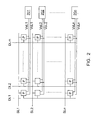
- FIG. 2 is a schematic view of the OLED panel according to the second embodiment of the invention.
- FIG. 3 is a schematic view illustrating first embodiment of partial circuit architecture of the OLED panel according to the invention.
- FIGS. 4A to 4D are illustrating an operation of a compensation circuit shown in FIG. 3 ;
- FIG. 5 is a schematic view illustrating second embodiment of the partial circuit architecture of the OLED panel according to the invention.
- FIG. 6 is a schematic view illustrating third embodiment of the partial circuit architecture of the OLED panel according to the invention.
- FIG. 7 is a schematic view illustrating fourth embodiment of the partial circuit architecture of the OLED panel according to the invention.
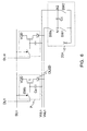
- FIG. 8A is a schematic view illustrating fifth embodiment of the partial circuit architecture of the OLED panel according to the invention.
- FIG. 8B is a schematic view illustrating sixth embodiment of the partial circuit architecture of the OLED panel according to the invention.
- FIG. 8C is a schematic view illustrating seventh embodiment of the partial circuit architecture of the OLED panel according to the invention.
- FIG. 8D is a schematic view illustrating eighth embodiment of the partial circuit architecture of the OLED panel according to the invention.
- FIG. 9 is a schematic view illustrating ninth embodiment of the partial circuit architecture of the OLED panel according to the invention.
- FIG. 10A is a schematic view illustrating the first embodiment of a switch controller in the OLED panel according to the invention.
- FIG. 10B is a schematic view illustrating the second embodiment of the switch controller in the OLED panel according to the invention.
- FIG. 10C is a schematic view illustrating the third embodiment of the switch controller in the OLED panel according to the invention.
- FIG. 11A is a schematic view illustrating the fourth embodiment of the switch controller in the OLED panel according to the invention.
- FIG. 11B is a schematic view illustrating the fifth embodiment of the switch controller in the OLED panel according to the invention.
- FIG. 11C is a schematic view illustrating the sixth embodiment of the switch controller in the OLED panel according to the invention.
- FIG. 12A is a schematic view illustrating the seventh embodiment of the switch controller in the OLED panel according to the invention.
- FIG. 12B is a schematic view illustrating the eighth embodiment of the switch controller in the OLED panel according to the invention.
- FIG. 12C is a schematic view illustrating the ninth embodiment of the switch controller in the OLED panel according to the invention.
- FIG. 13A is a schematic view illustrating the tenth embodiment of the switch controller in the OLED panel according to the invention.
- FIG. 13B is a schematic view illustrating the eleventh another embodiment of the switch controller in the OLED panel according to the invention.
- FIG. 13C is a schematic view illustrating the twelfth another embodiment of the switch controller in the OLED panel according to the invention.
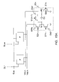
- FIG. 14A is a schematic view illustrating the first embodiment of the compensation circuit in the OLED panel according to the invention.
- FIG. 14B shows waveform of each signal in the switch controller shown in the FIG. 14A ;
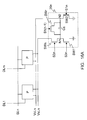
- FIG. 15A is a schematic view illustrating the second embodiment of the compensation circuit in the OLED panel according to the invention.
- FIG. 15B shows waveform of each signal in the switch controller shown in the FIG. 15A ;
- FIG. 16A is a schematic view illustrating the third embodiment of the compensation circuit in the OLED panel according to the invention.
- FIG. 16B shows waveform of each signal in the switch controller shown in the FIG. 16A ;
- FIG. 17 is a flow chart of a driving method of the OLED panel according to the first embodiment of the invention.
- FIG. 18 is a flow chart of a driving method of the OLED panel according to the second embodiment of the invention.
- FIG. 19 is a flow chart of a driving method of the OLED panel according to the third embodiment of the invention.
- FIG. 20 is a flow chart of a driving method of the OLED panel according to the fourth embodiment of the invention.
- FIG. 21 is a partial flow chart of a driving method of the OLED panel according to the fifth embodiment of the invention.
- FIG. 22 is a flow chart of a driving method of the OLED panel according to the sixth embodiment of the invention.
- FIG. 23 is a partial flow chart of a driving method of the OLED panel according to the seventh embodiment of the invention.
- FIG. 1 shows an OLED panel according to the invention.
- the OLED panel 10 comprises several data lines DL 1 to DLm, several scan lines SL 1 to SLn, several pixel P, several sampling voltage lines VsL 1 to VsLn and several compensation voltage lines VcL 1 to VcLn.
- the pixels P are defined by crossing the data lines DL 1 to DLm and the scan lines SL 1 to SLn in isolation. That is, each pixel P is defined by two neighboring data lines and two neighboring scan lines crossing two neighboring data lines.
- Each of the sampling voltage lines VsL 1 to VsLn is connected to a line unit of the pixels P, i.e. it is electrically connected to the pixels connecting to the same scan line.
- the compensation voltage lines VcL 1 to VcLn respectively correspond to the sampling voltage lines VsL 1 to VsLn, and are connected to the pixels P the same as the ones to which the corresponding sampling voltage lines VsL 1 to VsLn are connected.
- the pixels P connected to the same scan line are connected to the sampling voltage line and the compensation voltage line which correspond to each other.
- Each of the data lines DL 1 to DLm transmits a compensation signal
- the scan line SLn transmits a scan signal, such that small current flows through the organic light emitting diode (not shown) in the pixels P connected to the same scan line SLn.
- the sampling voltage line VsLn generates a compensation voltage in response to the compensation signals and threshold voltages of the driving transistors (not shown) and the organic light emitting diodes (not shown) in the pixels P connected thereto. Therefore, the corresponding compensation voltage line VcL 1 to VcLn adjusts the data signals transmitted from the data lines into the pixels P connected thereto in response to the compensation voltage.
- the compensation circuit compensates the threshold voltages of the transistors in the same line unit of the pixels P, i.e. the pixels P connected to the same scan line.
- the compensation circuits can be designed in non-illuminated region of the panel or be an element outside the panel.
- each of the pixels P includes a bias switch SWb, a storage capacitor Cs, a driving transistor T and an organic light emitting unit diode OLED.
- the gate of the driving transistor T is connected to the bias switch SWb, and the drain and source of the driving transistor T are respectively connected to a voltage source VDD and the organic light emitting diode OLED.
- the control terminal of the bias switch SWb is connected to the scan line, to electrically connect the data line and the control terminal of the driving transistor T, which are connected thereto, in response to the scan signal from the scan line connected thereto.
- the driving transistor T electrically connects the voltage source VDD and the organic light emitting diode OLED in response to the signal from the bias switch SWb, to control the current passing through the organic light emitting diode OLED.
- the storage capacitor Cs is connected between the compensation voltage line and the control terminal of the driving transistor T.
- Each of the compensation circuits 201 to 20 n includes a compensation capacitor Cc, a sampling switch SWs, a first switch SW 1 and a second switch SW 2 .
- the compensation circuit compensates the threshold voltages of the transistors in the line unit of the pixels by an external compensation capacitor Cc, i.e. utilizing the external compensation capacitor Cc to compensate the pixels P connected to the same scan line.
- the sampling switch SWs is connected between the sampling voltage lines VsLn and the first end N 1 of the compensation capacitor Cc
- the first switch SW 1 is connected between the first end N 1 of the compensation capacitor Cc and the ground
- the second switch SW 2 is connected between the second end N 2 of the compensation capacitor Cc and the ground
- the second end N 2 of the compensation capacitor Cc is connected to the compensation voltage lines VcLn.
- the sampling switch SWs and the second switch SW 2 of the compensation circuits 20 n are on and the first switch SW 1 of the compensation circuits 20 n is off.
- the voltage level of the compensation voltage lines VcLn is grounded, i.e.
- Vc_N 1 Vcomp ⁇ Vth_T ⁇ Vth_LU.
- the first switch SW 1 of the compensation circuits 20 n is on and the sampling switch SWs and the second switch SW 2 of the compensation circuits 20 n are off.
- the storage capacitor Cs in the pixels is connected to the compensation capacitor Cc of the external compensation circuit 20 n in series, and the polarity of the compensation capacitor Cc is reverse after the series connection, such that the voltage of the compensation voltage lines VcLn is that which is left by Vth_T+Vth_LU ⁇ Vcomp, i.e. the voltage of the compensation signal subtracted from the sum of the threshold voltages of the driving transistor T and the organic light emitting diodes OLED.
- the voltage stored in the storage capacitor Cs is the voltage of the data signal (Vdata).
- the voltage of the node N 3 is that which is left by the voltage of the compensation signal (Vcomp) subtracted from the sum of threshold voltages of the driving transistor T and the organic light emitting diodes OLED (Vth_T+Vth_OLED) and the voltage of the data signal (Vdata), i.e. Vth_T+Vth_OLED ⁇ Vcomp+Vdata.
- Vth_T+Vthe_OLED the voltage of the compensation voltage line VcLn
- Vth_T+Vthe_OLED the voltage of the compensation voltage line VcLn
- a reset switch SWr can be bridge connected with the compensation capacitor Cc, i.e. the reset switch SWr can be connected to the first end N 1 and the second end N 2 , to reset the compensation capacitor Cc.
- the sampling switch SWs, the first switch SW 1 and the reset switch SWr of the compensation circuits 20 n is on and the second switch SW 2 of the compensation circuits 20 n is off, to substantially completely discharge the compensation capacitor Cc.
- the first end N 1 of the compensation capacitor Cc also can be connected to a stable voltage V when the first switch SW 1 is on, and the second end N 2 of the compensation capacitor Cc also can be connected to the stable voltage V when the second switch SW 2 is on, as shown in FIG. 6 and FIG. 7 .
- the voltage source VDD and the stable voltage V can be from the same or different voltage source.
- a switch controller 30 can be used for controlling the sampling switch SWs, the first switch SW 1 and the second switch SW 2 , referring to FIG. 8A , FIG. 8B , FIG. 8C and FIG. 8D .
- the switch controller 30 can generate several control signals S 1 ( n -2), S 1 ( n -1), S 2 ( n -1), S 3 ( n -1), S 1 ( n -1), S 1 n, S 2 n and S 3 n in response to the scan signals S(n-1) and Sn.
- the switch controller can generate the control signals using at least an inverter and/or at least a shifter according to the types of the reset switches, the sampling switches, the first switches and the second switches.
- a inverter 31 inverts the scan signal Sn to generate two control signal S 1 n and S 2 n, so as to control the sampling switch, the first switch and the second switch in the compensation circuit 20 n.
- the control signal S 2 n can also be generated by a shifter 32 or combination of the inverter 31 and the shifter 32 , with reference to FIG. 10B and FIG. 10C .
- At least a buffer 33 is used for buffering the control signal S 1 n and S 2 n to be synchronize, referring to FIG. 11A , FIG. 11B and FIG. C.
- the switch controller 30 can generate the control signal S 2 n through the inverter 31 , the shifter 32 or the combination thereof according to the scan signals Sn and S(n-1), and transmit the control signal S 1 ( n -1), S 1 n and S 2 n, referring to FIG. 12A , FIG. 12B and FIG. 12C .
- the switch controller 30 can synchronize the control signals S 1 ( n -1), S 1 n and S 2 n to be transmitted using the buffer 33 , referring to FIG. 13A , FIG. 13B and FIG. 13C .
- the switch controller can invert the scan signal using the inverter, shift the phase of the scan signal using the buffer, and/or buffer the scan signal or the control signal to be transmitted using the buffer, to generate the control signals for controlling the compensation circuit.
- the reset switch, the sampling switch, the first switch and the second switch can be transistors, such as thin film transistors.
- the compensation circuit 20 n is controlled by three control signals S 1 ( n -1), S 1 n and S 2 n.
- the waveform of each signal is shown in FIG. 14B , where Data represents the data signal transmitted through the data lines DL 1 to DLm, Sn represents the scan signal transmitted through the n-th scan line SLn, and S(n-1) represents the scan signal transmitted through the (n-1)th scan line SL(n-1) (not shown).
- the control signal S 2 n is generated through shifting and inverting the scan signal Sn.
- the compensation circuit 20 n is controlled by three control signals S 1 ( n -1), S 1 n and S 2 n.
- the waveform of each signal is shown in FIG. 15B , where Data represents the data signal transmitted through the data lines DL 1 to DLm, Sn represents the scan signal transmitted through the n-th scan line SLn, and S(n-1) represents the scan signal transmitted through the (n-1)th scan line SL(n-1) (not shown).
- the control signal S 2 n is generated through shifting the scan signal Sn.
- the compensation circuit 20 n is controlled by four control signals S 1 ( n -1), S 1 n, S 2 n and S 3 n.
- the waveform of each signal is shown in FIG. 16B , where Data represents the data signal transmitted through the data lines DL 1 to DLm, Sn represents the scan signal transmitted through the n-th scan line SLn, and S(n-1) represents the scan signal transmitted through the (n-1)th scan line SL(n-1) (not shown).
- the control signal S 2 n is generated through shifting and inverting the scan signal Sn
- the control signal S 3 n is generated through inverting the scan signal Sn.
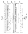
- the OLED panel has several pixels, each which is defined by two neighboring data lines and two neighboring scan lines crossing the two neighboring data lines, is connected to a data line and a scan line and comprises an organic light emitting diode, a driving transistor and a bias switch.
- the driving method comprises the following steps. First, a compensation signal is transmitted from the data line via the bias switch, to drive the driving transistor, such that the current flows through the organic light emitting diode (step 410 ). A compensation voltage is generated in response to threshold voltages of the driving transistors and the organic light emitting diodes in the pixels connected to the same scan line (step 420 ).
- a data signal is transmitted through the data line via the bias switch (step 430 ).
- the data signals, transmitted into the pixels which are connected to the same scan line, are adjusted in response to the compensation voltage (step 440 ).
- the driving transistor is drove in response to the adjusted data signal, to drive the organic light emitting diode (step 450 ).
- the compensation voltage can be generated in response to the compensation signal and the threshold voltages of the driving transistors and the organic light emitting diodes in the pixels connected to the same scan line (step 422 ), as shown in FIG. 18 .
- the voltage level of each of the data signals, transmitted into the pixels connected to the same scan line, is adjusted in response to the compensation voltage (step 442 ), as shown in FIG. 19 .
- FIG. 20 shows the driving method of the OLED panel according to the invention.
- the OLED panel has several pixels, each which is defined by two neighboring data lines and two neighboring scan lines crossing the two neighboring data lines, is connected to a data line and a scan line and comprises an organic light emitting diode, a driving transistor and a bias switch.
- the driving method comprises the following steps. First, a compensation signal is transmitted from the data line via the bias switch, to drive the driving transistor, such that the current flows through the organic light emitting diode (step 510 ). A compensation voltage in the first end of an external compensation capacitor is generated in response to threshold voltages of the driving transistors and the organic light emitting diodes in the pixels connected to the same scan lines (step 520 ).
- a data signal is transmitted through the data line via the bias switch (step 530 ).
- Each of the data signals which are transmitted into the pixels connected to the same scan lines, is adjusted via a second end of the external compensation capacitor in response to the compensation voltage (step 540 ).
- the driving transistor is drove in response to the adjusted data signal, to drive the organic light emitting diode (step 550 ).
- step 540 the following steps are included.
- the first end is grounded to generate a voltage level in response to the compensation voltage in the second end (step 542 ).
- step 544 each of the data signals, transmitted into the pixels connected to the same scan lines, are shifted in response to the voltage level (step 544 ).
- the compensation voltage can be generated in response to the compensation signal and the threshold voltages of the driving transistors and the organic light emitting diodes in the pixels connected to the same scan line (step 522 ), as shown in FIG. 22 .
- the driving method further comprises the following steps, as shown in FIG. 23 .
- the external compensation capacitor is reset (step 502 ), to substantially completely discharge the external compensation capacitor before driving.
Applications Claiming Priority (3)
| Application Number | Priority Date | Filing Date | Title |
|---|---|---|---|
| TW95126896 | 2006-07-24 | ||
| TW95126896A | 2006-07-24 | ||
| TW095126896A TWI343042B (en) | 2006-07-24 | 2006-07-24 | Light-emitting diode (led) panel and driving method thereof |
Publications (2)
| Publication Number | Publication Date |
|---|---|
| US20080018568A1 US20080018568A1 (en) | 2008-01-24 |
| US7956830B2 true US7956830B2 (en) | 2011-06-07 |
Family
ID=38970956
Family Applications (1)
| Application Number | Title | Priority Date | Filing Date |
|---|---|---|---|
| US11/739,777 Active 2030-03-21 US7956830B2 (en) | 2006-07-24 | 2007-04-25 | Organic light-emitting diode (OLED) panel and driving method with compensation voltage thereof |
Country Status (2)
| Country | Link |
|---|---|
| US (1) | US7956830B2 (zh) |
| TW (1) | TWI343042B (zh) |
Cited By (3)
| Publication number | Priority date | Publication date | Assignee | Title |
|---|---|---|---|---|
| US20100103082A1 (en) * | 2008-10-25 | 2010-04-29 | Levey Charles I | Electroluminescent display with initial nonuniformity compensation |
| US20100103159A1 (en) * | 2008-10-29 | 2010-04-29 | Leon Felipe A | Electroluminescent display with efficiency compensation |
| US20130162619A1 (en) * | 2011-12-27 | 2013-06-27 | Samsung Mobile Display Co., Ltd. | Display apparatus and method of repairing the same |
Families Citing this family (7)
| Publication number | Priority date | Publication date | Assignee | Title |
|---|---|---|---|---|
| TWI395174B (zh) * | 2008-11-11 | 2013-05-01 | Generalplus Technology Inc | 發光二極體陣列資訊輸入面板 |
| CN102654975B (zh) * | 2011-11-01 | 2014-08-20 | 京东方科技集团股份有限公司 | Amoled驱动补偿电路、方法及其显示装置 |
| TW201506881A (zh) * | 2013-08-02 | 2015-02-16 | Chunghwa Picture Tubes Ltd | 電壓補償方法及使用其之有機發光二極體顯示器 |
| US10445453B2 (en) * | 2015-04-08 | 2019-10-15 | Mediatek Inc. | Cell layout utilizing boundary cell with mixed poly pitch within integrated circuit |
| CN105243996B (zh) * | 2015-11-09 | 2018-01-30 | 深圳市华星光电技术有限公司 | 采用外部补偿的amoled驱动电路架构 |
| CN105469744B (zh) * | 2016-01-29 | 2018-09-18 | 深圳市华星光电技术有限公司 | 像素补偿电路、方法、扫描驱动电路及平面显示装置 |
| KR20210107225A (ko) * | 2020-02-21 | 2021-09-01 | 삼성디스플레이 주식회사 | 표시 장치 |
Citations (18)
| Publication number | Priority date | Publication date | Assignee | Title |
|---|---|---|---|---|
| KR20040008922A (ko) | 2002-07-19 | 2004-01-31 | 주식회사 하이닉스반도체 | 능동 방식 유기 el 디스플레이 장치 |
| US20040051685A1 (en) * | 2002-09-14 | 2004-03-18 | Choong-Heui Chung | Active matrix organic light emitting diode display panel circuit |
| US6774577B2 (en) * | 2002-07-24 | 2004-08-10 | Hynix Semiconductor Inc. | Flat panel display device for compensating threshold voltage of panel |
| US20050110730A1 (en) * | 2003-11-24 | 2005-05-26 | Yang-Wan Kim | Light emitting display and driving method thereof |
| KR20050080812A (ko) | 2004-02-11 | 2005-08-18 | 삼성에스디아이 주식회사 | 유기 전계 발광 소자 |
| US20050259051A1 (en) * | 2004-05-20 | 2005-11-24 | Samsung Electronics Co., Ltd | Display device and driving method thereof |
| US20050269959A1 (en) * | 2004-06-02 | 2005-12-08 | Sony Corporation | Pixel circuit, active matrix apparatus and display apparatus |
| US20050280614A1 (en) * | 2004-06-22 | 2005-12-22 | Samsung Electronics Co., Ltd. | Display device and a driving method thereof |
| US20060028408A1 (en) * | 2004-06-29 | 2006-02-09 | Kim Keum N | Light emitting diode display circuit with voltage drop compensation |
| US20060038501A1 (en) * | 2004-08-23 | 2006-02-23 | Jun Koyama | Display device, driving method of the same, and electronic device |
| US20060043375A1 (en) | 2004-08-31 | 2006-03-02 | Kyocera Corporation | Image display and method of driving image display |
| US20060061560A1 (en) * | 2004-09-17 | 2006-03-23 | Sony Corporation | Pixel circuit, display and driving method thereof |
| US20060066532A1 (en) | 2004-09-08 | 2006-03-30 | Jeong Jin T | Organic light emitting diode display |
| US20060108937A1 (en) * | 2004-11-08 | 2006-05-25 | Hong-Kwon Kim | Light emitting display and method of driving the same |
| US20060170628A1 (en) * | 2005-02-02 | 2006-08-03 | Sony Corporation | Pixel circuit, display and driving method thereof |
| US20070080908A1 (en) * | 2003-09-23 | 2007-04-12 | Arokia Nathan | Circuit and method for driving an array of light emitting pixels |
| US20070115225A1 (en) * | 2005-11-14 | 2007-05-24 | Sony Corporation | Display apparatus and driving method thereof |
| US7358938B2 (en) * | 2003-09-08 | 2008-04-15 | Samsung Sdi Co., Ltd. | Circuit and method for driving pixel of organic electroluminescent display |
-
2006
- 2006-07-24 TW TW095126896A patent/TWI343042B/zh active
-
2007
- 2007-04-25 US US11/739,777 patent/US7956830B2/en active Active
Patent Citations (18)
| Publication number | Priority date | Publication date | Assignee | Title |
|---|---|---|---|---|
| KR20040008922A (ko) | 2002-07-19 | 2004-01-31 | 주식회사 하이닉스반도체 | 능동 방식 유기 el 디스플레이 장치 |
| US6774577B2 (en) * | 2002-07-24 | 2004-08-10 | Hynix Semiconductor Inc. | Flat panel display device for compensating threshold voltage of panel |
| US20040051685A1 (en) * | 2002-09-14 | 2004-03-18 | Choong-Heui Chung | Active matrix organic light emitting diode display panel circuit |
| US7358938B2 (en) * | 2003-09-08 | 2008-04-15 | Samsung Sdi Co., Ltd. | Circuit and method for driving pixel of organic electroluminescent display |
| US20070080908A1 (en) * | 2003-09-23 | 2007-04-12 | Arokia Nathan | Circuit and method for driving an array of light emitting pixels |
| US20050110730A1 (en) * | 2003-11-24 | 2005-05-26 | Yang-Wan Kim | Light emitting display and driving method thereof |
| KR20050080812A (ko) | 2004-02-11 | 2005-08-18 | 삼성에스디아이 주식회사 | 유기 전계 발광 소자 |
| US20050259051A1 (en) * | 2004-05-20 | 2005-11-24 | Samsung Electronics Co., Ltd | Display device and driving method thereof |
| US20050269959A1 (en) * | 2004-06-02 | 2005-12-08 | Sony Corporation | Pixel circuit, active matrix apparatus and display apparatus |
| US20050280614A1 (en) * | 2004-06-22 | 2005-12-22 | Samsung Electronics Co., Ltd. | Display device and a driving method thereof |
| US20060028408A1 (en) * | 2004-06-29 | 2006-02-09 | Kim Keum N | Light emitting diode display circuit with voltage drop compensation |
| US20060038501A1 (en) * | 2004-08-23 | 2006-02-23 | Jun Koyama | Display device, driving method of the same, and electronic device |
| US20060043375A1 (en) | 2004-08-31 | 2006-03-02 | Kyocera Corporation | Image display and method of driving image display |
| US20060066532A1 (en) | 2004-09-08 | 2006-03-30 | Jeong Jin T | Organic light emitting diode display |
| US20060061560A1 (en) * | 2004-09-17 | 2006-03-23 | Sony Corporation | Pixel circuit, display and driving method thereof |
| US20060108937A1 (en) * | 2004-11-08 | 2006-05-25 | Hong-Kwon Kim | Light emitting display and method of driving the same |
| US20060170628A1 (en) * | 2005-02-02 | 2006-08-03 | Sony Corporation | Pixel circuit, display and driving method thereof |
| US20070115225A1 (en) * | 2005-11-14 | 2007-05-24 | Sony Corporation | Display apparatus and driving method thereof |
Non-Patent Citations (2)
| Title |
|---|
| English translation of abstract of KK 1020050080812. |
| English translation of abstract of KR 1020040008922. |
Cited By (6)
| Publication number | Priority date | Publication date | Assignee | Title |
|---|---|---|---|---|
| US20100103082A1 (en) * | 2008-10-25 | 2010-04-29 | Levey Charles I | Electroluminescent display with initial nonuniformity compensation |
| US8299983B2 (en) * | 2008-10-25 | 2012-10-30 | Global Oled Technology Llc | Electroluminescent display with initial nonuniformity compensation |
| US20100103159A1 (en) * | 2008-10-29 | 2010-04-29 | Leon Felipe A | Electroluminescent display with efficiency compensation |
| US8228267B2 (en) * | 2008-10-29 | 2012-07-24 | Global Oled Technology Llc | Electroluminescent display with efficiency compensation |
| US20130162619A1 (en) * | 2011-12-27 | 2013-06-27 | Samsung Mobile Display Co., Ltd. | Display apparatus and method of repairing the same |
| US8845378B2 (en) * | 2011-12-27 | 2014-09-30 | Samsung Display Co., Ltd. | Display apparatus and method of repairing the same |
Also Published As
| Publication number | Publication date |
|---|---|
| US20080018568A1 (en) | 2008-01-24 |
| TWI343042B (en) | 2011-06-01 |
| TW200807379A (en) | 2008-02-01 |
Similar Documents
| Publication | Publication Date | Title |
|---|---|---|
| US7956830B2 (en) | Organic light-emitting diode (OLED) panel and driving method with compensation voltage thereof | |
| US9741749B2 (en) | Digital circuit having correcting circuit and electronic apparatus thereof | |
| CN113129818B (zh) | 电致发光显示装置 | |
| CN100492477C (zh) | 发光显示器及其驱动方法 | |
| US8284128B2 (en) | Semiconductor device | |
| KR100637203B1 (ko) | 유기 전계발광 표시장치 및 그 동작방법 | |
| EP2299429B1 (en) | Semiconductor device | |
| US7459859B2 (en) | Organic light emitting display having organic light emitting diode circuit with voltage compensation and technique thereof | |
| US20070229417A1 (en) | Flexible Display Device | |
| EP3493191B1 (en) | Pixel and display device having the same | |
| US7586468B2 (en) | Display device using current driving pixels | |
| CN114255708A (zh) | 具有内部补偿的显示装置和像素单元 | |
| KR100502926B1 (ko) | 발광 표시 장치 및 그 표시 패널과 구동 방법 | |
| US10210799B2 (en) | Pixel compensation circuit and display device | |
| US7502002B2 (en) | Pixel circuit, electro-optical device, and electronic apparatus | |
| US11798497B2 (en) | Gate driving circuit and display device using the same | |
| CN112470210A (zh) | 时钟及电压生成电路和包括时钟及电压生成电路的显示装置 | |
| US20060186824A1 (en) | Pixel array and fabrication method thereof | |
| KR20160094472A (ko) | 전압선택장치 및 이를 포함하는 유기발광표시장치 | |
| CN114613333A (zh) | 像素和显示装置 |
Legal Events
| Date | Code | Title | Description |
|---|---|---|---|
| AS | Assignment |
Owner name: AU OPTRONICS CORP., TAIWAN Free format text: ASSIGNMENT OF ASSIGNORS INTEREST;ASSIGNORS:CHEN, YUNG-CHIH;LIN, CHIH-LUNG;WU, YUAN-CHUN;REEL/FRAME:019208/0614;SIGNING DATES FROM 20070407 TO 20070412 Owner name: AU OPTRONICS CORP., TAIWAN Free format text: ASSIGNMENT OF ASSIGNORS INTEREST;ASSIGNORS:CHEN, YUNG-CHIH;LIN, CHIH-LUNG;WU, YUAN-CHUN;SIGNING DATES FROM 20070407 TO 20070412;REEL/FRAME:019208/0614 |
|
| STCF | Information on status: patent grant |
Free format text: PATENTED CASE |
|
| FPAY | Fee payment |
Year of fee payment: 4 |
|
| MAFP | Maintenance fee payment |
Free format text: PAYMENT OF MAINTENANCE FEE, 8TH YEAR, LARGE ENTITY (ORIGINAL EVENT CODE: M1552); ENTITY STATUS OF PATENT OWNER: LARGE ENTITY Year of fee payment: 8 |
|
| MAFP | Maintenance fee payment |
Free format text: PAYMENT OF MAINTENANCE FEE, 12TH YEAR, LARGE ENTITY (ORIGINAL EVENT CODE: M1553); ENTITY STATUS OF PATENT OWNER: LARGE ENTITY Year of fee payment: 12 |