US7459859B2 - Organic light emitting display having organic light emitting diode circuit with voltage compensation and technique thereof - Google Patents
Organic light emitting display having organic light emitting diode circuit with voltage compensation and technique thereof Download PDFInfo
- Publication number
- US7459859B2 US7459859B2 US11/567,989 US56798906A US7459859B2 US 7459859 B2 US7459859 B2 US 7459859B2 US 56798906 A US56798906 A US 56798906A US 7459859 B2 US7459859 B2 US 7459859B2
- Authority
- US
- United States
- Prior art keywords
- tft
- voltage
- capacitor
- terminal
- receiving
- Prior art date
- Legal status (The legal status is an assumption and is not a legal conclusion. Google has not performed a legal analysis and makes no representation as to the accuracy of the status listed.)
- Active, expires
Links
Images


Classifications
-
- G—PHYSICS
- G09—EDUCATION; CRYPTOGRAPHY; DISPLAY; ADVERTISING; SEALS
- G09G—ARRANGEMENTS OR CIRCUITS FOR CONTROL OF INDICATING DEVICES USING STATIC MEANS TO PRESENT VARIABLE INFORMATION
- G09G3/00—Control arrangements or circuits, of interest only in connection with visual indicators other than cathode-ray tubes
- G09G3/20—Control arrangements or circuits, of interest only in connection with visual indicators other than cathode-ray tubes for presentation of an assembly of a number of characters, e.g. a page, by composing the assembly by combination of individual elements arranged in a matrix no fixed position being assigned to or needed to be assigned to the individual characters or partial characters
- G09G3/22—Control arrangements or circuits, of interest only in connection with visual indicators other than cathode-ray tubes for presentation of an assembly of a number of characters, e.g. a page, by composing the assembly by combination of individual elements arranged in a matrix no fixed position being assigned to or needed to be assigned to the individual characters or partial characters using controlled light sources
- G09G3/30—Control arrangements or circuits, of interest only in connection with visual indicators other than cathode-ray tubes for presentation of an assembly of a number of characters, e.g. a page, by composing the assembly by combination of individual elements arranged in a matrix no fixed position being assigned to or needed to be assigned to the individual characters or partial characters using controlled light sources using electroluminescent panels
- G09G3/32—Control arrangements or circuits, of interest only in connection with visual indicators other than cathode-ray tubes for presentation of an assembly of a number of characters, e.g. a page, by composing the assembly by combination of individual elements arranged in a matrix no fixed position being assigned to or needed to be assigned to the individual characters or partial characters using controlled light sources using electroluminescent panels semiconductive, e.g. using light-emitting diodes [LED]
- G09G3/3208—Control arrangements or circuits, of interest only in connection with visual indicators other than cathode-ray tubes for presentation of an assembly of a number of characters, e.g. a page, by composing the assembly by combination of individual elements arranged in a matrix no fixed position being assigned to or needed to be assigned to the individual characters or partial characters using controlled light sources using electroluminescent panels semiconductive, e.g. using light-emitting diodes [LED] organic, e.g. using organic light-emitting diodes [OLED]
- G09G3/3225—Control arrangements or circuits, of interest only in connection with visual indicators other than cathode-ray tubes for presentation of an assembly of a number of characters, e.g. a page, by composing the assembly by combination of individual elements arranged in a matrix no fixed position being assigned to or needed to be assigned to the individual characters or partial characters using controlled light sources using electroluminescent panels semiconductive, e.g. using light-emitting diodes [LED] organic, e.g. using organic light-emitting diodes [OLED] using an active matrix
- G09G3/3233—Control arrangements or circuits, of interest only in connection with visual indicators other than cathode-ray tubes for presentation of an assembly of a number of characters, e.g. a page, by composing the assembly by combination of individual elements arranged in a matrix no fixed position being assigned to or needed to be assigned to the individual characters or partial characters using controlled light sources using electroluminescent panels semiconductive, e.g. using light-emitting diodes [LED] organic, e.g. using organic light-emitting diodes [OLED] using an active matrix with pixel circuitry controlling the current through the light-emitting element
- G09G3/3241—Control arrangements or circuits, of interest only in connection with visual indicators other than cathode-ray tubes for presentation of an assembly of a number of characters, e.g. a page, by composing the assembly by combination of individual elements arranged in a matrix no fixed position being assigned to or needed to be assigned to the individual characters or partial characters using controlled light sources using electroluminescent panels semiconductive, e.g. using light-emitting diodes [LED] organic, e.g. using organic light-emitting diodes [OLED] using an active matrix with pixel circuitry controlling the current through the light-emitting element the current through the light-emitting element being set using a data current provided by the data driver, e.g. by using a two-transistor current mirror
-
- G—PHYSICS
- G09—EDUCATION; CRYPTOGRAPHY; DISPLAY; ADVERTISING; SEALS
- G09G—ARRANGEMENTS OR CIRCUITS FOR CONTROL OF INDICATING DEVICES USING STATIC MEANS TO PRESENT VARIABLE INFORMATION
- G09G2300/00—Aspects of the constitution of display devices
- G09G2300/08—Active matrix structure, i.e. with use of active elements, inclusive of non-linear two terminal elements, in the pixels together with light emitting or modulating elements
- G09G2300/0809—Several active elements per pixel in active matrix panels
- G09G2300/0819—Several active elements per pixel in active matrix panels used for counteracting undesired variations, e.g. feedback or autozeroing
-
- G—PHYSICS
- G09—EDUCATION; CRYPTOGRAPHY; DISPLAY; ADVERTISING; SEALS
- G09G—ARRANGEMENTS OR CIRCUITS FOR CONTROL OF INDICATING DEVICES USING STATIC MEANS TO PRESENT VARIABLE INFORMATION
- G09G2300/00—Aspects of the constitution of display devices
- G09G2300/08—Active matrix structure, i.e. with use of active elements, inclusive of non-linear two terminal elements, in the pixels together with light emitting or modulating elements
- G09G2300/0809—Several active elements per pixel in active matrix panels
- G09G2300/0842—Several active elements per pixel in active matrix panels forming a memory circuit, e.g. a dynamic memory with one capacitor
- G09G2300/0852—Several active elements per pixel in active matrix panels forming a memory circuit, e.g. a dynamic memory with one capacitor being a dynamic memory with more than one capacitor
-
- G—PHYSICS
- G09—EDUCATION; CRYPTOGRAPHY; DISPLAY; ADVERTISING; SEALS
- G09G—ARRANGEMENTS OR CIRCUITS FOR CONTROL OF INDICATING DEVICES USING STATIC MEANS TO PRESENT VARIABLE INFORMATION
- G09G2300/00—Aspects of the constitution of display devices
- G09G2300/08—Active matrix structure, i.e. with use of active elements, inclusive of non-linear two terminal elements, in the pixels together with light emitting or modulating elements
- G09G2300/0809—Several active elements per pixel in active matrix panels
- G09G2300/0842—Several active elements per pixel in active matrix panels forming a memory circuit, e.g. a dynamic memory with one capacitor
- G09G2300/0861—Several active elements per pixel in active matrix panels forming a memory circuit, e.g. a dynamic memory with one capacitor with additional control of the display period without amending the charge stored in a pixel memory, e.g. by means of additional select electrodes
- G09G2300/0866—Several active elements per pixel in active matrix panels forming a memory circuit, e.g. a dynamic memory with one capacitor with additional control of the display period without amending the charge stored in a pixel memory, e.g. by means of additional select electrodes by means of changes in the pixel supply voltage
-
- G—PHYSICS
- G09—EDUCATION; CRYPTOGRAPHY; DISPLAY; ADVERTISING; SEALS
- G09G—ARRANGEMENTS OR CIRCUITS FOR CONTROL OF INDICATING DEVICES USING STATIC MEANS TO PRESENT VARIABLE INFORMATION
- G09G2310/00—Command of the display device
- G09G2310/02—Addressing, scanning or driving the display screen or processing steps related thereto
- G09G2310/0243—Details of the generation of driving signals
- G09G2310/0251—Precharge or discharge of pixel before applying new pixel voltage
-
- G—PHYSICS
- G09—EDUCATION; CRYPTOGRAPHY; DISPLAY; ADVERTISING; SEALS
- G09G—ARRANGEMENTS OR CIRCUITS FOR CONTROL OF INDICATING DEVICES USING STATIC MEANS TO PRESENT VARIABLE INFORMATION
- G09G2320/00—Control of display operating conditions
- G09G2320/02—Improving the quality of display appearance
- G09G2320/0233—Improving the luminance or brightness uniformity across the screen
-
- G—PHYSICS
- G09—EDUCATION; CRYPTOGRAPHY; DISPLAY; ADVERTISING; SEALS
- G09G—ARRANGEMENTS OR CIRCUITS FOR CONTROL OF INDICATING DEVICES USING STATIC MEANS TO PRESENT VARIABLE INFORMATION
- G09G2320/00—Control of display operating conditions
- G09G2320/04—Maintaining the quality of display appearance
- G09G2320/043—Preventing or counteracting the effects of ageing
Definitions
- the invention relates in general to an organic light emitting display, and more particularly to an organic light emitting diode circuit for such a display.
- An organic light emitting diode circuit used in organic light emitting display normally stores signals for controlling the luminance of an organic light emitting diode (OLED) via thin film transistors (TFTs) and capacitors.
- TFTs thin film transistors
- Vth threshold voltage
- An organic light emitting diode circuit 100 includes TFTs MP 1 ⁇ MP 5 , a storage capacitor Cst and an organic light emitting diode (OLED).
- the TFT MP 3 is controlled by a scan signal Scan and the TFT MP 1 is coupled between the TFT MP 3 and the storage capacitor Cst.
- the TFT MP 2 drives the OLED to illuminate according to a voltage of the storage capacitor Cst when the TFT MP 4 is turned on.
- the TFT MP 5 is controlled by a reset signal Rst and the TFT MP 4 is controlled by an enable signal Enb.
- the conventional organic light emitting diode circuit 100 uses the TFT MP 1 with the same device feature as the TFT MP 2 to cancel the threshold voltage Vth 2 of the TFT MP 2 . More specifically, when the scan signal Scan is enabled, the TFT MP 3 is turned on and the pixel data Vdata charges the storage capacitor Cst via the TFTs MP 3 and MP 1 .
- the voltage level at point X that is, a gate voltage of the TFT MP 2
- a voltage level at point Y that is, a threshold voltage Vth 1 of the TFT MP 1
- Vth 1 the voltage difference between the source and gate of the TFT MP 2 is increased by Vth 1 .
- the threshold voltage Vth 1 is substantially the same as the threshold voltage Vth 2
- the voltage difference between the source and gate of the TFT MP 2 is just equal to difference between Vdd and the pixel voltage Vdata. Therefore, the current I OLED flowing by the OLED is precisely related to the pixel voltage Vdata.
- the compensation operation is performed during a data writing stage to eliminate errors generated from the threshold voltage Vth 2 .
- recent OLED panels tend to be developed in high resolution and large size. As a result, the time for writing data is greatly reduced.
- the TFT MP 1 has small current as it is turned on, and thus it needs longer compensation time, which will result in an irregular operation of the TFT MP 1 and disability of the compensation mechanism.
- the conventional voltage compensation arrangement is apt to exhibit the drawback that the the node X does not reach a stable voltage state for canceling Vth 2 due to inadequate time.
- the TFT MP 1 is still turned on.
- the charge sharing issue is generated and the display luminance can not reach the predicted luminance in correspondence with the pixel voltage Vdata.
- the invention is directed to an organic light emitting display and diode with a voltage compensation arrangement which improves the speed of threshold voltage compensation.
- an organic light emitting diode of an organic light emitting display equipped with a voltage compensation arrangement comprises a first capacitor, a first TFT, a second TFT, a third TFT, a reset circuit and an OLED.
- the first TFT has a first terminal for receiving a first reference voltage, and a second terminal coupled to its gate and a first end of the first capacitor.
- the second TFT has a first terminal for receiving a second reference voltage and a gate coupled to the gate of the first TFT.
- the third TFT has a first terminal for receiving a pixel voltage, a second terminal coupled to a second end of the first capacitor and a gate for receiving a scan signal.
- the reset circuit is for setting the first end of the first capacitor to have a first voltage level.
- the OLED has an anode coupled to a second terminal of the second TFT and a cathode for receiving a third reference voltage.
- the first voltage level is smaller than a voltage level of the first reference voltage.
- FIG. 1 is a circuit diagram of a conventional organic light emitting diode circuit.
- FIG. 2 is a schematic diagram of an organic light emitting display according to a first embodiment of the invention.
- FIG. 3 is a timing diagram of the organic light emitting diode circuit according to the first embodiment of the invention.
- FIG. 4 is another example of the reset circuit depicted in FIG. 2 .
- FIG. 5 is a further example of the reset circuit depicted in FIG. 2 .
- FIG. 6 is an internal circuit diagram of the organic light emitting diode circuit with a second storage capacitor according to the first embodiment of the invention.
- FIG. 7 is another example of the fifth TFT depicted in FIG. 2 .
- FIG. 8 is a further example of the fifth TFT depicted in FIG. 2 .
- FIG. 9 is yet another example of the fifth TFT depicted in FIG. 2 .
- FIG. 10 is an internal circuit diagram of the organic light emitting diode circuit equipped with a voltage compensation arrnagement.
- FIG. 11 is a timing diagram of the organic light emitting diode circuit according to a second embodiment of the invention.
- FIG. 12 is another example of the reset circuit depicted in FIG. 10 .
- FIG. 13 is another example of the reset circuit depicted in FIG. 10 .
- FIG. 14 is an internal circuit diagram of the organic light emitting diode circuit with a second storage capacitor according to the second embodiment of the invention.
- FIG. 15 is another example of the fifth TFT depicted in FIG. 10 .
- FIG. 16 is a further example of the fifth TFT depicted in FIG. 10 .
- FIG. 17 is yet another example of the fifth TFT depicted in FIG. 10 .
- the invention is directed to an organic light emitting display having a voltage compensation arrangement which improves the speed of threshold voltage compensation.
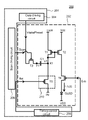
- FIG. 2 is a schematic diagram of an organic light emitting display according to a first embodiment of the invention.
- An organic light emitting display 200 includes a driving unit 201 and an organic light emitting diode circuit 202 .
- the driving unit 201 is for driving the organic light emitting diode circuit 202 and includes a data driving circuit 204 , scan driving circuit 206 and timing control circuit 208 .
- the data driving circuit 204 outputs a fifth voltage to the organic light emitting diode circuit 202 according to image data, wherein the fifth voltage is a pixel voltage Vdata or a low voltage Preset.
- the scan driving circuit 206 is for outputting a scan signal Scan.
- the timing control circuit 208 is configured to output a first control signal Enb to a fifth TFT T 5 and a second control signal Rst to a reset circuit 210 .
- the driving unit 201 also supplies a first voltage Lock, second voltage Vdd, third voltage Vss and fourth voltage INI.
- the organic light emitting diode circuit 202 includes a first capacitor C 1 , first TFT T 1 , second TFT T 2 , third TFT T 3 , fourth TFT T 4 , reset circuit 210 and an OLED.
- the TFTs T 1 ⁇ T 4 are exemplified to be p-typed metal oxide semiconductor (PMOS) transistors as shown in FIG. 2 .
- the third TFT T 3 has a first terminal for receiving the pixel voltage Vdata or the low voltage Preset, a second terminal coupled to a second end of the first capacitor C 1 (i.e. the node Y 1 denoted in FIG. 2 ) and a gate for receiving the scan signal Scan.
- the first TFT T 1 has a first terminal for receiving the first voltage Lock, and a second terminal and a gate coupled together to a first end of the first capacitor C 1 (i.e. the node X 1 denoted in FIG. 2 ).
- the second TFT T 2 has a first terminal for receiving the second voltage Vdd and a gate coupled to the gate of the first TFT T 1 .
- the fourth TFT T 4 has a first terminal coupled to a second terminal of the second TFT T 2 , a second terminal coupled to an anode of the OLED and a gate for receiving the first control signal Enb.
- a cathode of the OLED receives the third voltage Vss.
- the reset circuit 210 which is formed by the fifth TFT T 5 , is for setting the first end (i.e. the node X 1 ) of the first capacitor C 1 to have the first voltage level V 1 .
- the fifth TFT such as a PMOS transistor, has a first terminal coupled to the first end X 1 of the first capacitor C 1 , a second terminal for receiving the fourth voltage INI and a gate for receiving the second control signal Rst. It should be noted that the above first voltage level V 1 is smaller than a voltage level of the first voltage Lock.
- the scan signal Scan is set to have a voltage level such that the third TFT T 3 is turned off
- the second control signal Rst is set to have a voltage level such that the fifth TFT T 5 is turned off
- the first control signal Enb is set to have a voltage level such that the fourth TFT T 4 is turned on. Therefore, the voltage at the node Y 1 is a pixel voltage Vdata′ of the previous frame and the voltage at the node X 1 is a voltage X′ of the previous frame.
- the voltage X′ of the node X 1 is larger than the first voltage Lock.
- the first voltage Lock turns off the first TFT T 1 in the meanwhile the voltage X′ turns on the second TFT T 2 to generate a current I OLED .
- the current I OLED is equal to Kp*(Vsg ⁇ Vtp 2 ) 2 .
- the voltage Vsg is voltage difference between the gate and source of the second TFT T 2 , which is (Vdd ⁇ X′).
- the voltage Vtp 2 is a threshold voltage of the third TFT T 2 .
- the current I OLED drives the OLED to illuminate through the fourth TFT T 4 .
- the voltage level of the second control signal is set such that the fifth TFT T 5 is turned on
- the voltage level of the scan signal Scan is set such that the third TFT T 3 is turned on
- the voltage level of the first control signal Enb is set such that the fourth TFT T 4 is turned off.
- the data driving circuit 204 supplies a low voltage Preset.
- the low voltage Preset sets the voltage of the node Y 1 to be the predetermined low voltage Preset, such as ⁇ 1V ⁇ 0V through the turned-on third TFT T 3 .
- the voltage of the node X 1 is the fourth voltage INI due to turning on of the fifth TFT T 5 .
- the first capacitor C 1 is reset by the low voltage Preset and the fourth voltage INI.
- the voltage level of the second control signal is set such that the fifth TFT T 5 is turned off while the scan signal Scan and the first control signal Enb remain to have the same voltage level as in the previous stage. Therefore, the third TFT T 3 remains turned on and the fourth TFT T 4 remains turned off.
- the voltage of the node Y 1 is still the low voltage Preset and the voltage of the node X 1 rises up to a second voltage level V 2 due to the effect of the turned-off fifth TFT T 5 and the first TFT T 1 .
- the second voltage level V 2 is the first voltage Lock subtracted by the threshold voltage Vtp 1 of the first TFT T 1 .
- the voltage level of the control signal Enb is changed such that the fourth TFT T 4 is turned on, the second control signal Rst and scan signal Scan remain to have the same voltage level as in the second stage.
- the data driving circuit 204 outputs the pixel voltage Vdata.
- the voltage Vdata is provided through the third TFT T 3 to set the voltage of the node Y 1 as the pixel voltage Vdata.
- the voltage of the node X 1 also rises up to (Lock ⁇ Vtp 1 +Vdata ⁇ Preset) due to an effect of the first capacitor C 1 , which causes the first TFT T 1 to be turned off.
- the voltage difference between the gate and source of the second TFT T 2 is the second voltage Vdd subtracted by the voltage level of the node X 1 , i.e. Vdd ⁇ (Lock ⁇ Vtp 1 +Vdata ⁇ Preset).
- Vdd the voltage difference between the gate and source of the second TFT T 2 .
- the conductive current I OLED Kp*(Vsg ⁇ Vtp 2 ) 2 .
- the voltage difference Vsg is Vdd ⁇ (Lock ⁇ Vtp 1 +Vdata ⁇ Preset).
- the current I OLED Kp*(Vdd ⁇ (Lock ⁇ Vtp 1 +Vdata ⁇ Preset) ⁇ Vtp 2 ) 2 .
- Vtp 1 being approximately equal to Vtp 2
- the current I OLED can be approximated to be Kp*(Vdd ⁇ Lock ⁇ Vdata+Preset) 2 .
- the OLED thus has a luminance corresponding to the current I OLED .
- the organic light emitting diode circuit 202 has completed a compensation operation for the threshold voltage Vtp 2 .
- the operational speed of the compensation mechanism can be also increased to reduce compensation time. Owing to this fewer components are used in this embodiment and thus renders it more applicable to a small-size panel, such as in a hand-held equipment.
- another reset circuit 210 can be also implemented in a different circuit structure.
- another reset circuit 210 ′ consists of a fifth TFT T 5 wherein the fifth TFT T 5 has a first terminal coupled to the first end (i.e. the node X 1 ) of the first capacitor C 1 , and a second terminal and a gate coupled together for receiving the second control signal Rst.
- another reset circuit 210 ′′ also consists of the fifth TFT T 5 , but is such that it has a first terminal coupled to the first end (i.e. the node X 1 ) of the first capacitor C 1 , a second terminal coupled to the other end of the first capacitor C 1 and a gate for receiving the second control signal Rst.
- the organic light emitting diode circuit 202 can also be coupled to a second capacitor C 2 .
- the second capacitor C 2 has a first end coupled to the node Y 1 and a second end for receiving the second voltage Vdd.
- the second capacitor C 2 helps maintain a stable voltage difference between the nodes X 1 and Y 1 .
- the above fourth TFT T 4 is for controlling the current I OLED to flow toward the OLED. Except for the disposition position as shown in FIG. 2 , the fourth TFT T 4 can be also disposed at a position as shown in FIG. 7 .
- FIG. 7 is a schematic diagram of the second example of the organic light emitting display in the embodiment.
- the fourth TFT T 4 can also be disposed between the second voltage Vdd and the second TFT T 2 . That is, the fourth TFT T 4 has a first terminal for receiving the second voltage Vdd, a second terminal coupled to the first terminal (a source) of the second TFT T 2 and a gate for receiving the first control signal Enb.
- the fourth TFT T 4 can also be coupled outside the organic light emitting diode circuit for controlling the current I OLED to flow toward the OLED.
- FIG. 8 which is a schematic diagram of the third example of the organic light emitting display in the embodiment, the fourth TFT T 4 is coupled outside the organic light emitting diode circuit 802 . That is, the fourth TFT T 4 has a first terminal coupled to a cathode of the OLED, a second terminal coupled to the third voltage Vss and a gate for receiving the first control signal Enb.
- the fourth TFT T 4 can also be coupled outside the organic light emitting diode circuit and between the second voltage Vdd and second TFT T 2 .
- FIG. 9 which is a schematic diagram of the fourth example of the organic light emitting display of the first embodiment, the fourth TFT T 4 is coupled outside the organic light emitting diode circuit 902 and has a first terminal coupled to the first terminal of the second TFT T 2 , a second terminal coupled to the first voltage Vdd and a gate for receiving the first control signal Enb.
- the reset circuit consists of two TFTs which are respectively coupled to two ends of the first capacitor for resetting the first capacitor and setting a potential of the node X 1 .
- An organic light emitting display 1000 includes a driving unit 1001 and an organic light emitting diode circuit 1002 .
- the driving unit 1001 includes a data driving circuit 1004 , scan driving circuit 1006 and timing controller 1008 .
- the organic light emitting diode circuit 1002 also includes a first capacitor C 1 , a first TFT T 1 , a second TFT T 2 , a third TFT T 3 , a fourth TFT T 4 , a reset circuit 1010 and an OLED.
- the TFTs T 1 ⁇ T 4 are exemplified as PMOS transistors as shown in FIG. 10 .
- the organic light emitting display 1000 has the same structure as that in the first embodiment. Thus, details thereof are omitted for brevity.
- the reset circuit 1010 consists of a fifth TFT T 5 and sixth TFT T 6 .
- the fifth TFT T 5 and a sixth TFT T 6 are PMOS transistors by way of example only.
- the fifth TFT T 5 has a first terminal coupled to a first end (i.e. the node X 1 ) of the first capacitor C 1 , the second terminal for receiving the fourth voltage INI and a gate for receiving the second control signal Rst 1 .
- the sixth TFT T 6 has a first terminal coupled to a second end (i.e. the node Y 1 ) of the first capacitor C 1 , a second terminal for receiving the fourth voltage INI and a gate for receiving the third control signal Rst 2 .
- the first voltage level V 1 is smaller than a voltage level of the first voltage Lock.
- FIG. 11 a timing diagram of the organic light emitting diode circuit according to the second embodiment of the invention is shown.
- the voltage level of the scan signal Scan is set such that the third TFT T 3 is turned off
- the voltage levels of the second control signal Rst 1 and third control signal Rst 2 are set such that the fifth TFT T 5 and sixth TFT T 6 are both turned off. Therefore, the voltage of the node Y 1 is the pixel voltage Vdata′ of the previous frame and the voltage of the node X 1 is the voltage X′ of the previous frame.
- the voltage X′ of the node X 1 is larger than the first voltage Lock and thus the first TFT T 1 is turned off in the meanwhile the voltage X′ also turns on the second TFT T 2 to generate the current I OLED .
- the current I OLED is Kp*(Vdd ⁇ Y′ ⁇ Vtp 2 ) 2 .
- the voltage Vsg is voltage difference between the gate and source of the second TFT T 2 , which is Vdd ⁇ Y′.
- the voltage Vtp 2 is a threshold voltage of the second TFT T 2 .
- the current I OLED drives the OLED to illuminate through the fourth TFT T 4 .
- the voltage level of the scan signal Scan is changed such that the third TFT T 3 is turned off, the voltage levels of the second control signal Rst 1 and the third control signal Rst 2 are changed such that the fifth TFT T 5 and sixth TFT T 6 are both turned on.
- the voltage of the nodes X 1 and Y 1 is the fourth voltage INI, such as ⁇ 2V ⁇ 1V.
- the first capacitor C 1 is reset through the fourth voltage INI.
- the voltage level of the second control signal is changed such that the fifth TFT T 5 is turned off while the scan signal Scan, the first control signal Enb and the third control signal Rst 2 remain at the same voltage level as in the first stage (I Stage′). Therefore, at this time, the voltage of the node Y 1 is still INI and the voltage of the node X 1 rises up to a second voltage level V 2 due to an effect of the turned-off fifth TFT T 5 and the first TFT T 1 .
- the second voltage level V 2 is the first voltage Lock subtracted by the threshold voltage Vtp 1 of the first TFT T 1 . In other words, this stage is for setting the second end Y 1 of the first capacitor C 1 to have the voltage level Lock ⁇ Vtp 1 .
- the voltage level of the first control signal Enb is changed such that the fourth TFT T 4 is turned on
- the voltage level of the third control signal Rst 2 is changed such that the sixth TFT T 6 is turned off
- the voltage level of the scan signal Scan is changed such that the third TFT T 3 is turned on
- the second control signal Rst 1 remains at the original voltage level.
- the data driving circuit 1004 outputs the pixel voltage Vdata.
- the pixel voltage Vdata is provided through the turned-on third TFT T 3 to set the voltage of the node Y 1 as the pixel voltage Vdata.
- the voltage of the node X 1 also rises up to (Lock ⁇ Vtp 1 +Vdata ⁇ INI) due to an effect of the first capacitor C 1 , which causes the first TFT T 1 to be turned off.
- the voltage difference Vsg between the gate and source of the second TFT T 2 is the second voltage Vdd subtracted by the voltage level of the node X 1 , i.e. Vdd ⁇ (Lock ⁇ Vtp 1 +Vdata ⁇ INI).
- the fourth stage (IV Stage′) i.e. the frame display stage, except that the voltage level of the scan signal Scan is changed such that the third TFT T 3 is turned off and no pixel voltage is inputted to the third TFT T 3 , other components exhibit the same operation and the nodes have the same as in the third stage (III Stage′).
- the organic light emitting diode circuit 1002 has completed a compensation operation for the threshold voltage Vtp 2 .
- the operational speed of the compensation mechanism can be also increased to reduce compensation time. Owing to the fact that more components are used, this embodiment tends to be more applicable to large-size panels, such as in a display equipment.
- FIG. 12 another example of a reset circuit 1010 ′ consists of the fifth TFT T 5 and sixth TFT T 6 , wherein the fifth TFT T 5 has a first terminal coupled to the first end (i.e. the node X 1 ) of the first capacitor C 1 , and a second terminal for receiving the fourth voltage INI, and a gate for receiving the second control signal Rst 1 .
- the sixth TFT T 6 has a gate for receiving the third control signal Rst 2 .
- another reset circuit 1010 ′′ is also consisted of the fifth TFT T 5 and sixth TFT T 6 , but the fifth TFT T 5 has a first terminal coupled to the first end (i.e. the node X 1 ) of the first capacitor C 1 , and a second terminal and a gate coupled together for receiving the second control signal Rst 1 .
- the sixth TFT T 6 has a first terminal coupled to the second end (i.e. the node Y 1 ) of the first capacitor C 1 , a second terminal coupled and a gate together for receiving the third control signal Rst 2 .
- the organic light emitting diode circuit 1002 can also be coupled to a second capacitor C 2 .
- the second capacitor C 2 has a first end coupled to the node Y 1 and a second end for receiving the second voltage Vdd.
- the second capacitor C 2 helps maintain a stable voltage difference between the nodes X 1 and Y 1 .
- FIG. 15 is a schematic diagram of the second example of the organic light emitting display in the embodiment.
- the fourth TFT T 4 has a first terminal for receiving the second voltage Vdd, a second terminal coupled to the first terminal of the second TFT T 2 and a gate for receiving the first control signal Enb.
- the fourth TFT T 4 can also be coupled outside the organic light emitting diode circuit for controlling the current I OLED to flow toward the OLED.
- FIG. 16 which is a schematic diagram of the third example of the organic light emitting display in the embodiment, the fourth TFT T 4 is coupled outside the organic light emitting diode circuit 1602 .
- the fourth TFT T 4 has a first terminal coupled to a cathode of the OLED, a second terminal coupled to the third voltage Vss and a gate for receiving the first control signal Enb.
- the fourth TFT T 4 can also be coupled outside the organic light emitting diode circuit and between the second voltage Vdd and second TFT T 2 .
- FIG. 17 which is a schematic diagram of the fourth example of the organic light emitting display in the embodiment, the fourth TFT T 4 is coupled outside the organic light emitting diode circuit 1702 and has a first terminal coupled to the first terminal of the second TFT T 2 , a second terminal coupled to the first voltage Vdd and a gate for receiving the first control signal Enb.
- the organic light emitting display and the organic light emitting diode circuit with the voltage compensation technique disclosed in connection with the above embodiments of the invention can increase the speed of the compensation process and consequently eliminate the drawback of uneven frame display of an active matrix organic light emitting display (AMOLED) due to the present low-temperature poly-silicone technique.
- AMOLED active matrix organic light emitting display
Landscapes
- Engineering & Computer Science (AREA)
- Physics & Mathematics (AREA)
- Computer Hardware Design (AREA)
- General Physics & Mathematics (AREA)
- Theoretical Computer Science (AREA)
- Control Of Indicators Other Than Cathode Ray Tubes (AREA)
- Control Of El Displays (AREA)
- Electroluminescent Light Sources (AREA)
Abstract
Description
Claims (24)
Applications Claiming Priority (2)
| Application Number | Priority Date | Filing Date | Title |
|---|---|---|---|
| TW94143429 | 2005-12-08 | ||
| TW094143429A TWI272570B (en) | 2005-12-08 | 2005-12-08 | Organic light emitting display and pixel with voltage compensation technique thereof |
Publications (2)
| Publication Number | Publication Date |
|---|---|
| US20070159432A1 US20070159432A1 (en) | 2007-07-12 |
| US7459859B2 true US7459859B2 (en) | 2008-12-02 |
Family
ID=38232347
Family Applications (1)
| Application Number | Title | Priority Date | Filing Date |
|---|---|---|---|
| US11/567,989 Active 2027-08-07 US7459859B2 (en) | 2005-12-08 | 2006-12-07 | Organic light emitting display having organic light emitting diode circuit with voltage compensation and technique thereof |
Country Status (2)
| Country | Link |
|---|---|
| US (1) | US7459859B2 (en) |
| TW (1) | TWI272570B (en) |
Cited By (4)
| Publication number | Priority date | Publication date | Assignee | Title |
|---|---|---|---|---|
| US20070195019A1 (en) * | 2006-02-21 | 2007-08-23 | Shinya Ono | Image display apparatus |
| US20100164847A1 (en) * | 2008-12-29 | 2010-07-01 | Lee Baek-Woon | Display device and driving method thereof |
| US20150145754A1 (en) * | 2013-11-25 | 2015-05-28 | Sarnsung Display Co., Ltd. | Pixel circuit for increasing accuracy of current sensing |
| US10615189B2 (en) * | 2011-10-18 | 2020-04-07 | Semiconductor Energy Laboratory Co., Ltd. | Semiconductor device |
Families Citing this family (16)
| Publication number | Priority date | Publication date | Assignee | Title |
|---|---|---|---|---|
| KR100821046B1 (en) * | 2006-12-19 | 2008-04-08 | 삼성에스디아이 주식회사 | Pixel and organic light emitting display using the same |
| US7768483B2 (en) * | 2007-07-02 | 2010-08-03 | Tpo Displays Corp. | Pixels and display panels |
| JP5186950B2 (en) * | 2008-02-28 | 2013-04-24 | ソニー株式会社 | EL display panel, electronic device, and driving method of EL display panel |
| JP5217500B2 (en) * | 2008-02-28 | 2013-06-19 | ソニー株式会社 | EL display panel module, EL display panel, integrated circuit device, electronic apparatus, and drive control method |
| TWI383355B (en) * | 2008-05-27 | 2013-01-21 | Univ Nat Cheng Kung | A driving circuit and a pixel circuit having the driving circuit |
| JP5286992B2 (en) * | 2008-07-09 | 2013-09-11 | セイコーエプソン株式会社 | Electro-optical device and electronic apparatus |
| TWI406228B (en) * | 2010-07-08 | 2013-08-21 | Au Optronics Corp | Pixel structure and pixel structure of organic emitting device |
| TWI484468B (en) * | 2010-11-30 | 2015-05-11 | Univ Nat Cheng Kung | Flexible display and controlling method thereof |
| CN107016962B (en) * | 2013-03-28 | 2020-03-17 | 群创光电股份有限公司 | Pixel circuit, driving method thereof and display panel |
| TWI479468B (en) * | 2013-06-17 | 2015-04-01 | Innolux Corp | Pixel and display device utilizing the same |
| CN103474026B (en) * | 2013-09-06 | 2015-08-19 | 京东方科技集团股份有限公司 | A kind of image element circuit and display |
| CN104637446B (en) * | 2015-02-03 | 2017-10-24 | 北京大学深圳研究生院 | Image element circuit and its driving method and a kind of display device |
| CN104680980B (en) * | 2015-03-25 | 2017-02-15 | 京东方科技集团股份有限公司 | Pixel driving circuit, driving method thereof and display device |
| CN104680981B (en) * | 2015-03-26 | 2017-03-15 | 京东方科技集团股份有限公司 | OLED pixel drive circuit and driving method, OLED display |
| TWI571854B (en) * | 2015-12-30 | 2017-02-21 | 友達光電股份有限公司 | Light-emitting diode device control method |
| CN107919091B (en) * | 2018-01-03 | 2019-11-22 | 京东方科技集团股份有限公司 | A kind of OLED pixel driving circuit and driving method, OLED display |
Citations (3)
| Publication number | Priority date | Publication date | Assignee | Title |
|---|---|---|---|---|
| US7046240B2 (en) * | 2001-08-29 | 2006-05-16 | Semiconductor Energy Laboratory Co., Ltd. | Light emitting device, method of driving a light emitting device, element substrate, and electronic equipment |
| US7245278B2 (en) * | 2003-09-12 | 2007-07-17 | Au Optronics Corporation | Light emitting device and method of driving thereof |
| US7420530B2 (en) * | 2005-05-12 | 2008-09-02 | Sony Corporation | Pixel circuit, display device method for controlling pixel circuit |
-
2005
- 2005-12-08 TW TW094143429A patent/TWI272570B/en not_active IP Right Cessation
-
2006
- 2006-12-07 US US11/567,989 patent/US7459859B2/en active Active
Patent Citations (3)
| Publication number | Priority date | Publication date | Assignee | Title |
|---|---|---|---|---|
| US7046240B2 (en) * | 2001-08-29 | 2006-05-16 | Semiconductor Energy Laboratory Co., Ltd. | Light emitting device, method of driving a light emitting device, element substrate, and electronic equipment |
| US7245278B2 (en) * | 2003-09-12 | 2007-07-17 | Au Optronics Corporation | Light emitting device and method of driving thereof |
| US7420530B2 (en) * | 2005-05-12 | 2008-09-02 | Sony Corporation | Pixel circuit, display device method for controlling pixel circuit |
Cited By (9)
| Publication number | Priority date | Publication date | Assignee | Title |
|---|---|---|---|---|
| US20070195019A1 (en) * | 2006-02-21 | 2007-08-23 | Shinya Ono | Image display apparatus |
| US20100164847A1 (en) * | 2008-12-29 | 2010-07-01 | Lee Baek-Woon | Display device and driving method thereof |
| US8289313B2 (en) | 2008-12-29 | 2012-10-16 | Samsung Electronics Co., Ltd. | Display device and driving method thereof |
| US8736589B2 (en) | 2008-12-29 | 2014-05-27 | Samsung Display Co., Ltd. | Display device and driving method thereof |
| US10615189B2 (en) * | 2011-10-18 | 2020-04-07 | Semiconductor Energy Laboratory Co., Ltd. | Semiconductor device |
| US11587957B2 (en) * | 2011-10-18 | 2023-02-21 | Semiconductor Energy Laboratory Co., Ltd. | Semiconductor device |
| US20150145754A1 (en) * | 2013-11-25 | 2015-05-28 | Sarnsung Display Co., Ltd. | Pixel circuit for increasing accuracy of current sensing |
| US9373282B2 (en) * | 2013-11-25 | 2016-06-21 | Samsung Display Co., Ltd. | Pixel circuit for increasing accuracy of current sensing |
| US9514681B2 (en) | 2013-11-25 | 2016-12-06 | Samsung Display Co., Ltd. | Pixel circuit for increasing accuracy of current sensing |
Also Published As
| Publication number | Publication date |
|---|---|
| TW200723227A (en) | 2007-06-16 |
| TWI272570B (en) | 2007-02-01 |
| US20070159432A1 (en) | 2007-07-12 |
Similar Documents
| Publication | Publication Date | Title |
|---|---|---|
| US7459859B2 (en) | Organic light emitting display having organic light emitting diode circuit with voltage compensation and technique thereof | |
| US11887546B2 (en) | Electronic display with hybrid in-pixel and external compensation | |
| US9601057B2 (en) | Pixel circuit, organic electroluminesce display panel and display device | |
| US10565933B2 (en) | Pixel circuit, driving method thereof, array substrate, display device | |
| US9984626B2 (en) | Pixel circuit for organic light emitting diode, a display device having pixel circuit and driving method of pixel circuit | |
| CN107945737B (en) | Pixel compensation circuit, driving method thereof, display panel and display device | |
| US9047814B2 (en) | Pixel circuit, display device, electronic apparatus, and method of driving pixel circuit | |
| US7800556B2 (en) | Organic light emitting diode display and pixel driving method thereof | |
| US20170178569A1 (en) | Pixel circuit and driving method thereof, array substrate, display device | |
| US20200342812A1 (en) | Pixel driving circuit, driving method thereof, display device | |
| US20070273618A1 (en) | Pixels and display panels | |
| JP2007108378A (en) | Driving method of display device and display device | |
| JP2008170788A (en) | Image display device | |
| US10565926B2 (en) | OLED pixel circuit and driving method and related display panel and display apparatus | |
| US10665163B2 (en) | Pixel circuit, driving method thereof, array substrate and display device | |
| US8624801B2 (en) | Pixel structure having a transistor gate voltage set by a reference voltage | |
| JP2018105917A (en) | Display panel and display device | |
| JP2019082548A (en) | Pixel circuit, display device, driving method of pixel circuit, and electronic apparatus | |
| JP2008052279A (en) | Image display system | |
| US7683863B2 (en) | Organic light emitting diode display and pixel circuit thereof | |
| JP4984863B2 (en) | Display device and driving method thereof | |
| CN101140733A (en) | Driver circuit having electromechanical excitation light dipolar body and driving method thereof | |
| JP5034208B2 (en) | Display device and driving method of display device | |
| US10685601B2 (en) | Pixel circuit and display unit | |
| US10818242B2 (en) | Pixel circuit including plurality of switching transistors and capacitors, and display unit |
Legal Events
| Date | Code | Title | Description |
|---|---|---|---|
| AS | Assignment |
Owner name: CHI MEI OPTOELECTRONICS CORP., TAIWAN Free format text: ASSIGNMENT OF ASSIGNORS INTEREST;ASSIGNORS:TSENG, MING-CHUN;GUO, HONG-RU;HUANG, CHIEN-HSIANG;REEL/FRAME:018991/0029 Effective date: 20070118 Owner name: CHI MEI EL CORPORATION, TAIWAN Free format text: ASSIGNMENT OF ASSIGNORS INTEREST;ASSIGNORS:TSENG, MING-CHUN;GUO, HONG-RU;HUANG, CHIEN-HSIANG;REEL/FRAME:018991/0029 Effective date: 20070118 |
|
| STCF | Information on status: patent grant |
Free format text: PATENTED CASE |
|
| AS | Assignment |
Owner name: CHIMEI INNOLUX CORPORATION,TAIWAN Free format text: MERGER;ASSIGNOR:CHI MEI OPTOELECTRONICS CORP.;REEL/FRAME:024358/0272 Effective date: 20100318 Owner name: CHIMEI INNOLUX CORPORATION, TAIWAN Free format text: MERGER;ASSIGNOR:CHI MEI OPTOELECTRONICS CORP.;REEL/FRAME:024358/0272 Effective date: 20100318 |
|
| FPAY | Fee payment |
Year of fee payment: 4 |
|
| AS | Assignment |
Owner name: INNOLUX CORPORATION, TAIWAN Free format text: CHANGE OF NAME;ASSIGNOR:CHIMEI INNOLUX CORPORATION;REEL/FRAME:032621/0718 Effective date: 20121219 |
|
| FPAY | Fee payment |
Year of fee payment: 8 |
|
| MAFP | Maintenance fee payment |
Free format text: PAYMENT OF MAINTENANCE FEE, 12TH YEAR, LARGE ENTITY (ORIGINAL EVENT CODE: M1553); ENTITY STATUS OF PATENT OWNER: LARGE ENTITY Year of fee payment: 12 |