US7919829B2 - Liner for shallow trench isolation - Google Patents
Liner for shallow trench isolation Download PDFInfo
- Publication number
- US7919829B2 US7919829B2 US11/846,427 US84642707A US7919829B2 US 7919829 B2 US7919829 B2 US 7919829B2 US 84642707 A US84642707 A US 84642707A US 7919829 B2 US7919829 B2 US 7919829B2
- Authority
- US
- United States
- Prior art keywords
- trench
- silicon
- layer
- nitride layer
- silicon nitride
- Prior art date
- Legal status (The legal status is an assumption and is not a legal conclusion. Google has not performed a legal analysis and makes no representation as to the accuracy of the status listed.)
- Expired - Lifetime, expires
Links
Images


Classifications
-
- H—ELECTRICITY
- H10—SEMICONDUCTOR DEVICES; ELECTRIC SOLID-STATE DEVICES NOT OTHERWISE PROVIDED FOR
- H10W—GENERIC PACKAGES, INTERCONNECTIONS, CONNECTORS OR OTHER CONSTRUCTIONAL DETAILS OF DEVICES COVERED BY CLASS H10
- H10W10/00—Isolation regions in semiconductor bodies between components of integrated devices
- H10W10/01—Manufacture or treatment
- H10W10/011—Manufacture or treatment of isolation regions comprising dielectric materials
- H10W10/014—Manufacture or treatment of isolation regions comprising dielectric materials using trench refilling with dielectric materials, e.g. shallow trench isolations
-
- H—ELECTRICITY
- H10—SEMICONDUCTOR DEVICES; ELECTRIC SOLID-STATE DEVICES NOT OTHERWISE PROVIDED FOR
- H10W—GENERIC PACKAGES, INTERCONNECTIONS, CONNECTORS OR OTHER CONSTRUCTIONAL DETAILS OF DEVICES COVERED BY CLASS H10
- H10W10/00—Isolation regions in semiconductor bodies between components of integrated devices
- H10W10/10—Isolation regions comprising dielectric materials
- H10W10/17—Isolation regions comprising dielectric materials formed using trench refilling with dielectric materials, e.g. shallow trench isolations
-
- H—ELECTRICITY
- H10—SEMICONDUCTOR DEVICES; ELECTRIC SOLID-STATE DEVICES NOT OTHERWISE PROVIDED FOR
- H10W—GENERIC PACKAGES, INTERCONNECTIONS, CONNECTORS OR OTHER CONSTRUCTIONAL DETAILS OF DEVICES COVERED BY CLASS H10
- H10W10/00—Isolation regions in semiconductor bodies between components of integrated devices
- H10W10/01—Manufacture or treatment
- H10W10/011—Manufacture or treatment of isolation regions comprising dielectric materials
- H10W10/014—Manufacture or treatment of isolation regions comprising dielectric materials using trench refilling with dielectric materials, e.g. shallow trench isolations
- H10W10/0142—Manufacture or treatment of isolation regions comprising dielectric materials using trench refilling with dielectric materials, e.g. shallow trench isolations the dielectric materials being chemical transformed from non-dielectric materials
Definitions
- This invention relates generally to the field of integrated circuit fabrication, and more specifically to trench isolation and methods therefor.
- Trench isolation is the practice of creating trenches in the substrate in order to separate electrical components on the chip.
- the trenches are typically filled with an insulator that will prevent cross-talk between transistors.
- Shallow trench isolation which is becoming quite prevalent in modern IC design, uses trenches that are substantially narrower than previous isolation technology, such as LOCal Oxidation of Silicon (LOCOS).
- LOCOS LOCal Oxidation of Silicon
- the size can vary, but a trench less than one half of a micron wide has become quite common.
- STI also offers smaller channel width encroachment and better planarity than technologies used in earlier IC generations.
- a silicon nitride liner in an STI trench has substantial stress-relieving capabilities for the sidewalls of the trench.
- Such liners are often used for high density ICs, such as dynamic random access memory (DRAM) chips, to protect the bulk silicon during subsequent process steps.
- DRAM dynamic random access memory
- the trench is then typically filled with an insulator such as a form of silicon oxide.
- the oxide can be deposited in a number of methods, such as CVD, sputtering, or a spin-on deposition process.
- Spin-on insulators, or spin-on dielectrics (SOD) can be deposited evenly. Additionally, SOD materials, which often form silicon oxide after being reacted, carry less risk of voids in the resulting insulating material than other deposition processes.
- the SOD precursor is reacted to form silicon oxide using a high temperature oxidation process.
- an isolation structure for an integrated circuit comprises a trench formed within a substrate.
- the trench has sidewalls and a base.
- a silicon nitride layer is within the trench.
- a portion of the silicon nitride layer at the sidewalls and base of the trench has a higher level of nitrogen than a portion of the silicon nitride layer most removed from the sidewalls and the base of the trench.
- An insulating material is within the silicon nitride layer.
- a method of forming an isolation structure comprises forming a recess with a base and sidewalls within a substrate.
- a first nitride layer is deposited within the recess and a depositing a silicon-rich second nitride layer is deposited over the first nitride layer.
- a insulator precursor within the second nitride layer is deposited.
- a method of isolating electrical components in an integrated circuit comprises forming a trench within a substrate.
- a silicon nitride layer is deposited within and lining the trench.
- the silicon nitride layer is deposited by adjusting the deposition of the silicon nitride layer to produce a lower nitrogen content in an interior portion of the nitride layer compared to an outside portion of the silicon nitride layer.
- a silicon oxide precursor is deposited within the silicon nitride layer.
- a method of isolating electrical components on a substrate comprises forming a recess in the substrate and depositing a graded silicon nitride layer within the recess. Depositing the silicon nitride layer comprises decreasing a nitrogen percentage while depositing the silicon nitride layer. An insulation precursor is deposited after depositing the silicon nitride layer. An insulator is formed from the insulation precursor.
- a method of forming an isolation trench in an integrated circuit comprises forming a trench in a substrate.
- the trench is lined with a silicon nitride layer, wherein the silicon nitride layer has a nitrogen content by atomic weight of less than 34%.
- the method further comprises depositing an insulator in the trench after lining the trench
- a method of forming an isolation trench is disclosed in another aspect of the invention.
- the method comprises lining a trench with a barrier layer and depositing an adhesion layer over the barrier layer.
- the adhesion layer has a silicon content by weight of between about 66% and 88%.
- the method further comprises depositing a spin-on insulation precursor in the recess after depositing the adhesion layer.
- An insulator is formed from the insulation precursor.
- FIG. 1 is a schematic, cross-sectional side view of a substrate with a thin “pad oxide” grown over the surface of the substrate, a thicker layer of silicon nitride (Si 3 N 4 ), and a photoresist mask in accordance with a starting point for preferred embodiments of the present invention.
- FIG. 2 is a schematic, cross-sectional side view of the substrate of FIG. 1 after a trench has been formed.
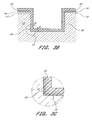
- FIG. 3A is a schematic, cross-sectional side view of the substrate of FIG. 2 with a silicon nitride bilayer within the recess according to an embodiment of the present invention.
- FIG. 3B is a schematic, cross-sectional side view of the substrate of FIG. 2 with a graded silicon nitride layer within the recess according to another embodiment of the present invention.
- FIG. 3C is a close-up view of schematic, cross-sectional side view of the substrate of FIG. 3B with a graded silicon nitride layer.
- FIG. 3D is a schematic, cross-sectional side view of the substrate of FIG. 2 with a silicon nitride tri-layer within the recess according to an embodiment of the present invention.
- FIG. 3E is a close-up view of schematic, cross-sectional side view of the substrate of FIG. 3D .
- FIG. 4 is a schematic, cross-sectional side view of the substrate of FIG. 3A with a layer of spin-on dielectric material filling the trench.
- FIG. 5 is a schematic, cross-sectional side view of the substrate of FIG. 4 after a curing and densification process.
- FIG. 6 is a schematic, cross-sectional side view of the substrate of FIG. 5 after etching back the oxide down to the top nitride surface.
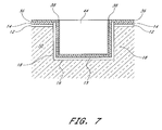
- FIG. 7 is a schematic, cross-sectional side view of a substrate with an isolation trench with a graded nitride layer according to a preferred embodiment.
- Shallow trench isolation (STI) trenches in dynamic random access memory devices are typically lined with a silicon nitride layer.
- silicon oxide formed from a spin-on dielectric (SOD) precursor has been found to adhere poorly to conventional barrier materials, such as stoichiometric silicon nitride, Si 3 N 4 .
- a nitrogen-poor material will not effectively protect the trench and the active area of the bulk silicon from damage from processing.
- the adhesion problem is due to poor re-bonding, which makes the interface between the silicon oxide and the silicon nitride weak.
- the SOD precursor bonds with the walls of the surrounding material to form a blended interface which provides a stable isolation structure.
- the weakest bonds those between silicon and hydrogen, are broken down first.
- a silicon-rich surface is provided as an underlayer for the formation of a SOD layer, more silicon is available for re-bonding at the silicon nitride/silicon oxide interface.
- the preferred embodiments provide a higher silicon content near the interior of the trench.
- the portions of the liner closest to the trench walls and base comprise a silicon nitride with a relatively lower silicon content.
- the spin-on dielectric precursor is deposited after forming the liner and is reacted to form an insulator for the STI trench.
- a highly silicon-based adhesion layer also helps alleviate insulator shrinkage problems that can arise from the densification process.
- An etch-back step such as chemical mechanical polishing (CMP), can then be used to smooth the trench surface.
- CMP chemical mechanical polishing
- An introductory step is the creation of a trench, preferably for shallow trench isolation (STI).
- the trench can be of varying widths, but in a preferred embodiment, the trench is less than a micron wide.
- a semiconductor substrate 10 e.g., a silicon wafer
- a thin “pad” oxide 12 is thermally grown on the substrate.
- a thicker layer of a silicon nitride 14 preferably Si 3 N 4 , is formed over the pad oxide 12 .
- the nitride 14 is preferably formed by chemical vapor deposition (CVD). This nitride layer 14 acts as a stop for a subsequent etch back, such as a CMP process.
- Exemplary thickness ranges are between about 30 ⁇ and 100 ⁇ for the pad oxide 12 and between about 200 ⁇ and 1500 ⁇ for the nitride layer 14 .
- a photoresist mask 16 is applied the substrate 10 in order to etch the trench.
- Photoresist is applied on the surface of the wafer.
- a reticle that blocks ultraviolet (UV) radiation is then placed over the wafer.
- the photoresist is then selectively exposed to UV radiation.
- the developing solution washes away either exposed or unexposed regions.
- a recess preferably a trench for isolation, is formed in the substrate.
- the photoresist mask 16 of FIG. 2 is removed by conventional resist strip process.
- the trench depth is preferably between about 1,000 ⁇ and 10,000 ⁇ , more preferably between about 2,500 ⁇ and 6,000 ⁇ .
- the trench can also be formed through the use of a hard mask or by other methods. The skilled practitioner will appreciate that the trench can be formed by several different procedures.
- the trench is preferably etched by an anisotropic etch, i.e. a directional etch, which produces relatively straight, vertical sidewalls.
- An exemplary etch process is reactive ion etch (RIE). As shown in FIG. 2 , this method is quite accurate and straight. However, RIE can also damage the edges of transistor active areas, defined by the sidewalls 18 of the trench.
- the sidewalls 18 and base 19 are oxidized, forming a thin oxide layer in order to repair any damage from the anisotropic etch process.
- a silicon nitride layer is deposited to line the trench.
- the nitride layer can be deposited by any of a variety of deposition methods, including CVD, atomic layer deposition (ALD), and sputtering.
- An additional method of deposition is ion-metal plasma deposition, a sputtering process with magnetic collimation. While silicon nitride deposited by CVD is described here, other materials and deposition processes can be used to form a liner layer.
- Stoichiometric silicon nitride (Si 3 N 4 ) has a silicon content of approximately 60% by weight, and a nitrogen content of about 40% by weight.
- the silicon content closest to the trench sidewall 18 is lower than the silicon content in the portion of the nitride layer farthest from the trench sidewalls 18 .
- the nitrogen content of the nitride layer close to the trench sidewalls 18 is higher than the nitrogen content near the interior of the trench.
- the nitride liners are formed by a CVD process.
- nitrogen precursors include ammonia (NH 3 ), which is a widely used precursor for many deposition processes, and nitrogen (N 2 ), which is used in processes such as plasma CVD.
- exemplary silicon precursors include dichlorosilane (DCS) and other silane compounds.
- DCS and NH 3 are used together to form a silicon nitride liner. The combination of these two precursors provides an excellent layer at relatively low temperatures.
- the nitride layer can be deposited in several different methods.
- the nitride layer can be deposited in a single wafer chamber.
- the proportion of the precursors can be adjusted during the deposition of the nitride layer.
- the nitride layer deposition can begin with a DCS flow rate of approximately 90 sccm, and a NH 3 flow rate of approximately 270 sccm.
- these flow rates will generally form a layer that is approximately stoichiometric silicon nitride (Si 3 N 4 ) and has approximately 60% silicon by atomic weight.
- the nitrogen source flow is reduced, relative to the silicon flow, or the silicon flow is increased relative to the nitrogen flow.
- the DCS flow rate is preferably approximately 180 sccm, and the ammonia flow rate is unchanged.
- a nitride layer formed with these settings will be substantially more silicon-rich at approximately Si 3 N 2 , and a silicon content of approximately 80% by atomic weight.
- the transition between these states can be accomplished in several methods. Distinct layers with increasing silicon content can be formed by stepped changes.
- the nitride layer is formed as a bilayer 20 and 30 in two deposition steps.
- the nitrogen content of the nitride layer 22 is gradually decreased.
- the resulting nitride layer 22 has smoothly graded nitrogen and silicon percentages.
- a nitrogen-rich layer 21 is formed in the trench.
- a nitrogen-graded layer 25 is formed over the “nitrogen-rich” layer 21 .
- a silicon-rich nitride layer 31 is formed over the graded layer 25 . Skilled practitioners will appreciate that there are a myriad of methods and patterns for decreasing the relative nitrogen content of the nitride layer or increasing the relative silicon content.
- the liner layer ( 20 in FIG. 3A ) closest to the trench walls 18 and base 19 preferably acts as a barrier layer.
- the nitrogen content by atomic weight close to the trench walls 18 is preferably between about 36% and 52%, more preferably between about 39% and 48%.
- the silicon content by atomic weight close to the trench walls is preferably between about 48% and 64%, more preferably between about 52% and 61%.
- the liner layer ( 30 in FIG. 3A ) furthest from the trench walls 18 preferably acts as an adhesion layer.
- the silicon content by atomic weight in this adhesion layer is preferably between about 66% and 88%, more preferably between about 73% and 85%.
- the nitrogen content by atomic weight of the adhesion layer is preferably less than about 35%, more preferably between about 12% and 34%, most preferably between about 15% and 27%.
- the barrier layer and the adhesion layer need not be separate and distinct layers.
- the liner is deposited in the trench in two steps.
- a “nitrogen-rich” layer 20 is deposited, followed by a silicon-rich layer 30 .
- the nitrogen-rich layer 20 is between about 30 ⁇ and 200 ⁇ thick, more preferably between about 50 ⁇ and 100 ⁇ .
- this nitrogen-rich 20 layer is deposited by CVD.
- the gas flow for ammonia (NH 3 ) is preferably between about 200 sccm and 340 sccm.
- the gas flow rate for dichlorosilane is preferably between about 50 sccm and 135 sccm.
- a preferred ratio of nitrogen precursor to silicon precursor is between about 2.5:1 and 3.5:1, more preferably between about 2.7:1 and 3.3:1.
- the temperature in a single wafer CVD chamber is between about 500° C. and 900° C., more preferably between about 600° C. and 800° C.
- the “silicon-rich” layer 30 is preferably thinner than the nitrogen-rich layer 20 at between about 5 ⁇ and 100 ⁇ thick, more preferably between about 10 ⁇ and 20 ⁇ .
- the ratio of nitrogen precursor to silicon precursor for the silicon-rich layer 30 preferably decreases from the ratio of the nitrogen-rich layer 20 by between about 40% and 60%, more preferably by between about 45% and 55%.
- a preferred ratio of nitrogen precursor to silicon precursor is between about 1.1:1 and 2:1, more preferably between about 1.3:1 and 1.8:1.
- the gas flow for ammonia is preferably between about 200 sccm and 340 sccm.
- the gas flow rate for DCS is preferably between about 140 sccm and 220 sccm.
- the temperature in a single wafer CVD chamber is preferably maintained between about 500° C. and 900° C., more preferably between about 600° C. and 800° C.
- a nitride layer is formed using two deposition steps as described above.
- a 60 ⁇ thick “nitrogen-rich” layer 20 was formed during a CVD process.
- the deposition process took 60 minutes to form using gas flow rates of 270 sccm of ammonia and 90 sccm of DCS.
- the gas flow rates are then adjusted to 270 sccm of ammonia and 180 sccm of DCS.
- the silicon-rich layer 30 is formed in a process that takes 60 minutes to form a 60 ⁇ thick layer.
- the temperature of the chamber was about 600° C. in this example.
- the nitrogen content in the nitride layer 22 is graded down from a high level near the walls 18 and floor 19 of the trench, gradually decreasing as the deposition process continues.
- the deposition process is not stopped to change the gas flow rates; rather, the flow rates are adjusted during the deposition process.
- the nitrogen and silicon content of the nitride layer 22 is discussed above.
- the flow rates begin at rates similar to the rates of the “nitrogen-rich” layer 20 described in reference to the embodiment of FIG. 3A , and end at rates similar to the rates for the “silicon-rich” layer 30 in that embodiment.
- the gradient will be linear across the entire nitride layer 22 .
- Other gradient profiles can also be formed depending upon the operation of the deposition, specifically the adjustment of the flow rates.
- the nitride layer consists of three layers.
- the layer closest to the trench walls 18 will be a “nitrogen-rich” layer 21 , as in previous embodiments.
- the nitrogen content close to the trench walls 18 and floor 19 is similar to previous embodiments.
- this layer is between about 5 ⁇ and 20 ⁇ thick, more preferably between about 10 ⁇ and 15 ⁇ .
- An intermediate layer 25 will be graded from nitrogen-rich to silicon-rich, similar to the embodiments described with reference to FIGS. 3B and 3C .
- the gradient profile can be linear or nonlinear depending upon the flow rates and other operation factors of the deposition equipment.
- the graded layer is between about 10 ⁇ and 100 ⁇ thick, more preferably between about 20 ⁇ and 50 ⁇ .
- An outer layer will be a silicon-rich layer 31 with a thickness of between about 5 ⁇ and 20 ⁇ , more preferably between about 10 ⁇ and 15 ⁇ .
- the thickness of the trilayer is preferably similar to the total thickness of the nitride layer of previous embodiments.
- the trench can be filled with an insulator.
- the insulator is a non-conductive oxide, such as silicon oxide.
- the trench is filled with a spin on material.
- an insulator precursor material 40 has been deposited within the trench.
- a spin-on deposition process is preferably used to deposit the precursor 40 into the remaining space in the trench, as shown in FIG. 4 .
- the thickness of the precursor 40 will vary based upon the size of the trench, but in the illustrated embodiment the thickness of the material is preferably between 2500 ⁇ and 5500 ⁇ , more preferably between 3000 ⁇ and 4500 ⁇ .
- Spin-on deposition uses liquid materials dripped on the substrate after formation of the isolation trenches. The wafer is rapidly spun, which spreads the liquid uniformly over the surface of the wafer after filling the low points on the wafer.
- An example of a spin-on material is SpinfilTM made by Clariant (Japan) K.K.-Life Science & Electronic Chemicals of Tokyo, Japan. This product is a polysilazane based inorganic spin-on dielectric precursor. However, the skilled practitioner will appreciate that many dielectric materials can be used for these purposes.
- Clariant's SpinfilTM SOD precursor based upon perhydrosilazane (SiH 2 NH), has a recommended conversion/densification recipe as follows:
- a more preferred densification process is described in an application by Smythe, et al. (filed Feb. 19, 2004, application Ser. No. 10/782,997), which is hereby incorporated by reference.
- the densification process of that application uses a ramped temperature process.
- a prepared wafer is placed in a chamber.
- the wafer is preferably heated to an initial temperature of between about 200° C. and 600° C., more preferably between 300° C. and 500° C.
- steam is then turned on in the chamber. From the initial temperature, the heat ramps up to a target temperature between approximately 800° C. and 1200° C., more preferably between 900° C. and 1100° C., and most preferably between 950° C. and 1050° C.
- the increase of the temperature in the chamber is stopped when it gets to this target temperature.
- the temperature can increase approximately between about 3° C. per minute to 25° C. per minute, more preferably between about 8° C. and 20° C.
- the wafer is in an oxidizing environment, preferably an ambient steam environment.
- the wafer is annealed for approximately 10 to 40 minutes, more preferably between 15 min and 35 min, at the temperature plateau on steady state.
- the wafer is annealed in a second oxidizing environment, preferably in a dry oxygen (O 2 ) environment.
- O 2 dry oxygen
- FIG. 5 shows the trench and surrounding area after the conversion process. Because the portion of the nitride layer 30 ( FIG. 4 ) that is in contact with the insulating precursor 40 ( FIG. 4 ) was silicon-rich, the interface between the resulting insulator 44 and the liner layer 34 will be smooth.
- the densification process consumes some of the silicon from the silicon-rich layer 30 ( FIG. 4 ) and leaves a less silicon-rich layer 34 and a layer of silicon oxynitride (SiON) 38 at the interface of the silicon nitride layer 34 and the densified silicon oxide insulator 44 .
- SiON silicon oxynitride
- the oxide 44 in the trench is preferably etched back with a chemical mechanical polishing (CMP) process.
- CMP chemical mechanical polishing
- the CMP process preferably stops on the silicon nitride layer 34 when using a two layer silicon nitride layer.
- the silicon nitride layer 30 is particularly silicon-rich or was substantially oxidized by the densification process, the CMP process can be stopped by the “nitrogen-rich” silicon nitride layer 20 .
- the CMP process can also stop within the silicon nitride layer.
- FIG. 6 An embodiment is seen in FIG. 6 after an etch back of the oxide.
- the trench is preferably filled without voids, which can negatively affect the isolation effects of the trench.
- the spin-on material 44 has been reacted into silicon oxide, which provides excellent insulation.
- the silicon oxide 44 adheres well to the surface of the remaining silicon nitride layer 34 .
- a silicon oxynitride layer 38 is formed at the interface of the silicon oxide 44 and the nitride layer 34 .
- the silicon oxynitride layer is between about 5 ⁇ and 20 ⁇ thick, more preferably between about 10 ⁇ and 15 ⁇ .
- the nitrogen content gradient and silicon content gradient of the nitride layers 20 and 34 in the completed trench structure can be substantially altered.
- the nitrogen gradient may be somewhat smoothed by diffusion between the “nitrogen-rich” layer 20 and the remaining silicon-rich layer 34 .
- the silicon-rich layer 34 preferably has a higher silicon content than the nitrogen-rich layer 20 .
- the nitrogen-rich layer 20 will have between about 48% and 64% silicon by atomic weight, more preferably between about 52% and 61% silicon by atomic weight.
- the remaining silicon-rich layer 34 will have preferably between about 50% and 85% silicon by atomic weight, more preferably between about 60% and 80% silicon by atomic weight, and most preferably between about 70% and 75% silicon by atomic weight.
- FIG. 7 is an illustration of a trench using a nitride liner 22 similar to that of FIG. 3B .
- the trench has been filled with an oxide 44 , which has been etched back.
- the graded nitride layer 36 has provided an adhesion layer for formation of the oxide 44 .
- the portion of a resultant nitride layer 36 closest to the trench walls 18 and base 19 will have between about 48% and 64% silicon by atomic weight, more preferably between about 52% and 61% silicon by atomic weight.
- the portion of the nitride layer 36 furthest from the trench walls 18 and base 19 will have preferably between about 50% and 85% silicon by atomic weight, more preferably between about 60% and 80% silicon by atomic weight, and most preferably between about 70% and 75% silicon by atomic weight.
- FIG. 7 illustrates an oxide layer 15 along the walls 18 and base 19 of the trench resulting from oxidizing the surfaces of the trench before depositing a graded nitride liner 22 similar to that of FIG. 3B .
- the oxide layer 15 preferably has a thickness of between about 30 ⁇ and 100 ⁇ .
- the oxidation of the trench walls 18 and base 19 serves to repair damage from the trench formation.
- the oxide layer 15 also protects the active areas in the substrate 10 from damage that might be caused during processing.
- a similar oxide layer can be formed in other embodiments described herein.
Landscapes
- Element Separation (AREA)
- Formation Of Insulating Films (AREA)
Abstract
Description
SixNyHz+H2O→SiO2+H2+NH3
Claims (9)
Priority Applications (1)
| Application Number | Priority Date | Filing Date | Title |
|---|---|---|---|
| US11/846,427 US7919829B2 (en) | 2004-08-24 | 2007-08-28 | Liner for shallow trench isolation |
Applications Claiming Priority (2)
| Application Number | Priority Date | Filing Date | Title |
|---|---|---|---|
| US10/925,715 US7271464B2 (en) | 2004-08-24 | 2004-08-24 | Liner for shallow trench isolation |
| US11/846,427 US7919829B2 (en) | 2004-08-24 | 2007-08-28 | Liner for shallow trench isolation |
Related Parent Applications (1)
| Application Number | Title | Priority Date | Filing Date |
|---|---|---|---|
| US10/925,715 Continuation US7271464B2 (en) | 2004-08-24 | 2004-08-24 | Liner for shallow trench isolation |
Publications (2)
| Publication Number | Publication Date |
|---|---|
| US20070290293A1 US20070290293A1 (en) | 2007-12-20 |
| US7919829B2 true US7919829B2 (en) | 2011-04-05 |
Family
ID=35941882
Family Applications (3)
| Application Number | Title | Priority Date | Filing Date |
|---|---|---|---|
| US10/925,715 Expired - Lifetime US7271464B2 (en) | 2004-08-24 | 2004-08-24 | Liner for shallow trench isolation |
| US11/470,150 Expired - Lifetime US7514366B2 (en) | 2004-08-24 | 2006-09-05 | Methods for forming shallow trench isolation |
| US11/846,427 Expired - Lifetime US7919829B2 (en) | 2004-08-24 | 2007-08-28 | Liner for shallow trench isolation |
Family Applications Before (2)
| Application Number | Title | Priority Date | Filing Date |
|---|---|---|---|
| US10/925,715 Expired - Lifetime US7271464B2 (en) | 2004-08-24 | 2004-08-24 | Liner for shallow trench isolation |
| US11/470,150 Expired - Lifetime US7514366B2 (en) | 2004-08-24 | 2006-09-05 | Methods for forming shallow trench isolation |
Country Status (1)
| Country | Link |
|---|---|
| US (3) | US7271464B2 (en) |
Cited By (4)
| Publication number | Priority date | Publication date | Assignee | Title |
|---|---|---|---|---|
| CN104051500A (en) * | 2013-03-12 | 2014-09-17 | 旺宏电子股份有限公司 | Semiconductor device and method for manufacturing the same |
| US20170033179A1 (en) * | 2015-07-29 | 2017-02-02 | Taiwan Semiconductor Manufacturing Co., Ltd. | Trench structure of semiconductor device and manufacturing method thereof |
| CN108987333A (en) * | 2018-07-20 | 2018-12-11 | 上海华力微电子有限公司 | A kind of forming method and fleet plough groove isolation structure of fleet plough groove isolation structure |
| US11251189B2 (en) | 2009-02-09 | 2022-02-15 | Longitude Flash Memory Solutions Ltd. | Gate fringing effect based channel formation for semiconductor device |
Families Citing this family (55)
| Publication number | Priority date | Publication date | Assignee | Title |
|---|---|---|---|---|
| JP2006278745A (en) * | 2005-03-29 | 2006-10-12 | Matsushita Electric Ind Co Ltd | Semiconductor device manufacturing method and semiconductor device |
| US8501632B2 (en) * | 2005-12-20 | 2013-08-06 | Infineon Technologies Ag | Methods of fabricating isolation regions of semiconductor devices and structures thereof |
| JP4984558B2 (en) * | 2006-02-08 | 2012-07-25 | 富士通セミコンダクター株式会社 | Manufacturing method of semiconductor device |
| US7767515B2 (en) * | 2006-02-27 | 2010-08-03 | Synopsys, Inc. | Managing integrated circuit stress using stress adjustment trenches |
| US8936995B2 (en) * | 2006-03-01 | 2015-01-20 | Infineon Technologies Ag | Methods of fabricating isolation regions of semiconductor devices and structures thereof |
| KR100831676B1 (en) * | 2006-06-30 | 2008-05-22 | 주식회사 하이닉스반도체 | Device Separation Method of Semiconductor Device |
| US20080227267A1 (en) * | 2007-03-14 | 2008-09-18 | Theodorus Gerardus Maria Oosterlaken | Stop mechanism for trench reshaping process |
| US7691693B2 (en) * | 2007-06-01 | 2010-04-06 | Synopsys, Inc. | Method for suppressing layout sensitivity of threshold voltage in a transistor array |
| US7892942B2 (en) * | 2007-07-09 | 2011-02-22 | Micron Technology Inc. | Methods of forming semiconductor constructions, and methods of forming isolation regions |
| US7895548B2 (en) * | 2007-10-26 | 2011-02-22 | Synopsys, Inc. | Filler cells for design optimization in a place-and-route system |
| US20090108408A1 (en) * | 2007-10-29 | 2009-04-30 | Synopsys, Inc. | Method for Trapping Implant Damage in a Semiconductor Substrate |
| US9472423B2 (en) * | 2007-10-30 | 2016-10-18 | Synopsys, Inc. | Method for suppressing lattice defects in a semiconductor substrate |
| KR101003494B1 (en) * | 2008-04-10 | 2010-12-30 | 주식회사 하이닉스반도체 | Device Separation Structure and Formation Method of Memory Devices |
| JP2010098293A (en) * | 2008-09-22 | 2010-04-30 | Elpida Memory Inc | Semiconductor device |
| US8216904B2 (en) * | 2008-12-31 | 2012-07-10 | St Microelectronics, Inc. | Strained transistor and method for forming the same |
| US7998359B2 (en) * | 2010-09-24 | 2011-08-16 | Innovalight, Inc. | Methods of etching silicon-containing films on silicon substrates |
| US8030170B2 (en) * | 2009-12-08 | 2011-10-04 | Micron Technology, Inc. | Methods of forming isolation structures, and methods of forming nonvolatile memory |
| US8048755B2 (en) | 2010-02-08 | 2011-11-01 | Micron Technology, Inc. | Resistive memory and methods of processing resistive memory |
| US8921183B2 (en) * | 2010-12-08 | 2014-12-30 | Nanya Technology Corporation | Method for fabricating trench isolation structure |
| US8765561B2 (en) | 2011-06-06 | 2014-07-01 | United Microelectronics Corp. | Method for fabricating semiconductor device |
| US8921944B2 (en) | 2011-07-19 | 2014-12-30 | United Microelectronics Corp. | Semiconductor device |
| US8647941B2 (en) | 2011-08-17 | 2014-02-11 | United Microelectronics Corp. | Method of forming semiconductor device |
| US8691659B2 (en) | 2011-10-26 | 2014-04-08 | United Microelectronics Corp. | Method for forming void-free dielectric layer |
| US8592328B2 (en) | 2012-01-20 | 2013-11-26 | Novellus Systems, Inc. | Method for depositing a chlorine-free conformal sin film |
| US8835243B2 (en) | 2012-05-04 | 2014-09-16 | United Microelectronics Corp. | Semiconductor process |
| US8772120B2 (en) | 2012-05-24 | 2014-07-08 | United Microelectronics Corp. | Semiconductor process |
| US8772904B2 (en) * | 2012-06-13 | 2014-07-08 | United Microelectronics Corp. | Semiconductor structure and process thereof |
| US8951876B2 (en) | 2012-06-20 | 2015-02-10 | United Microelectronics Corp. | Semiconductor device and manufacturing method thereof |
| US9142400B1 (en) | 2012-07-17 | 2015-09-22 | Stc.Unm | Method of making a heteroepitaxial layer on a seed area |
| WO2014131461A1 (en) * | 2013-02-28 | 2014-09-04 | Commissariat à l'énergie atomique et aux énergies alternatives | Dual sti integrated circuit including fdsoi transistors and method for manufacturing the same |
| US8962430B2 (en) | 2013-05-31 | 2015-02-24 | Stmicroelectronics, Inc. | Method for the formation of a protective dual liner for a shallow trench isolation structure |
| US20140374838A1 (en) * | 2013-06-21 | 2014-12-25 | Taiwan Semiconductor Manufacturing Company, Ltd. | FinFETs with Nitride Liners and Methods of Forming the Same |
| US8895396B1 (en) | 2013-07-11 | 2014-11-25 | United Microelectronics Corp. | Epitaxial Process of forming stress inducing epitaxial layers in source and drain regions of PMOS and NMOS structures |
| KR102246280B1 (en) * | 2014-03-26 | 2021-04-29 | 에스케이하이닉스 주식회사 | Semiconductor device and method for fabricating the same |
| US9214333B1 (en) * | 2014-09-24 | 2015-12-15 | Lam Research Corporation | Methods and apparatuses for uniform reduction of the in-feature wet etch rate of a silicon nitride film formed by ALD |
| US9589790B2 (en) | 2014-11-24 | 2017-03-07 | Lam Research Corporation | Method of depositing ammonia free and chlorine free conformal silicon nitride film |
| US9564312B2 (en) | 2014-11-24 | 2017-02-07 | Lam Research Corporation | Selective inhibition in atomic layer deposition of silicon-containing films |
| US9502238B2 (en) | 2015-04-03 | 2016-11-22 | Lam Research Corporation | Deposition of conformal films by atomic layer deposition and atomic layer etch |
| US9601693B1 (en) | 2015-09-24 | 2017-03-21 | Lam Research Corporation | Method for encapsulating a chalcogenide material |
| JP6509095B2 (en) * | 2015-11-04 | 2019-05-08 | 東京エレクトロン株式会社 | Method of forming nitride film |
| US9406617B1 (en) * | 2015-11-19 | 2016-08-02 | International Business Machines Corporation | Structure and process for W contacts |
| US10629435B2 (en) | 2016-07-29 | 2020-04-21 | Lam Research Corporation | Doped ALD films for semiconductor patterning applications |
| US10074543B2 (en) | 2016-08-31 | 2018-09-11 | Lam Research Corporation | High dry etch rate materials for semiconductor patterning applications |
| US9865455B1 (en) | 2016-09-07 | 2018-01-09 | Lam Research Corporation | Nitride film formed by plasma-enhanced and thermal atomic layer deposition process |
| US10454029B2 (en) | 2016-11-11 | 2019-10-22 | Lam Research Corporation | Method for reducing the wet etch rate of a sin film without damaging the underlying substrate |
| US10832908B2 (en) | 2016-11-11 | 2020-11-10 | Lam Research Corporation | Self-aligned multi-patterning process flow with ALD gapfill spacer mask |
| US10134579B2 (en) | 2016-11-14 | 2018-11-20 | Lam Research Corporation | Method for high modulus ALD SiO2 spacer |
| US10269559B2 (en) | 2017-09-13 | 2019-04-23 | Lam Research Corporation | Dielectric gapfill of high aspect ratio features utilizing a sacrificial etch cap layer |
| CN112005343B (en) | 2018-03-02 | 2025-05-06 | 朗姆研究公司 | Selective deposition using hydrolysis |
| WO2020247977A1 (en) | 2019-06-04 | 2020-12-10 | Lam Research Corporation | Polymerization protective liner for reactive ion etch in patterning |
| WO2021025874A1 (en) | 2019-08-06 | 2021-02-11 | Lam Research Corporation | Thermal atomic layer deposition of silicon-containing films |
| JP7278184B2 (en) * | 2019-09-13 | 2023-05-19 | キオクシア株式会社 | Semiconductor device manufacturing method |
| CN115735261A (en) | 2020-07-28 | 2023-03-03 | 朗姆研究公司 | Reduction of impurities in silicon-containing films |
| US12027374B2 (en) * | 2021-04-30 | 2024-07-02 | Applied Materials, Inc. | Processes to deposit amorphous-silicon etch protection liner |
| JP2024524553A (en) | 2021-07-09 | 2024-07-05 | ラム リサーチ コーポレーション | Plasma-enhanced atomic layer deposition of silicon-containing films |
Citations (35)
| Publication number | Priority date | Publication date | Assignee | Title |
|---|---|---|---|---|
| US4855804A (en) * | 1987-11-17 | 1989-08-08 | Motorola, Inc. | Multilayer trench isolation process and structure |
| US5087586A (en) | 1991-07-03 | 1992-02-11 | Micron Technology, Inc. | Process for creating fully-recessed field isolation regions by oxidizing a selectively-grown epitaxial silicon layer |
| US5190889A (en) | 1991-12-09 | 1993-03-02 | Motorola, Inc. | Method of forming trench isolation structure with germanium silicate filling |
| US5229316A (en) | 1992-04-16 | 1993-07-20 | Micron Technology, Inc. | Semiconductor processing method for forming substrate isolation trenches |
| US5387540A (en) | 1993-09-30 | 1995-02-07 | Motorola Inc. | Method of forming trench isolation structure in an integrated circuit |
| US5447884A (en) | 1994-06-29 | 1995-09-05 | International Business Machines Corporation | Shallow trench isolation with thin nitride liner |
| US5492858A (en) | 1994-04-20 | 1996-02-20 | Digital Equipment Corporation | Shallow trench isolation process for high aspect ratio trenches |
| US5702976A (en) | 1995-10-24 | 1997-12-30 | Micron Technology, Inc. | Shallow trench isolation using low dielectric constant insulator |
| US5869384A (en) | 1997-03-17 | 1999-02-09 | Taiwan Semiconductor Manufacturing Company, Ltd. | Trench filling method employing silicon liner layer and gap filling silicon oxide trench fill layer |
| US5926717A (en) | 1996-12-10 | 1999-07-20 | Advanced Micro Devices, Inc. | Method of making an integrated circuit with oxidizable trench liner |
| US5943585A (en) | 1997-12-19 | 1999-08-24 | Advanced Micro Devices, Inc. | Trench isolation structure having low K dielectric spacers arranged upon an oxide liner incorporated with nitrogen |
| US6027982A (en) | 1999-02-05 | 2000-02-22 | Chartered Semiconductor Manufacturing Ltd. | Method to form shallow trench isolation structures with improved isolation fill and surface planarity |
| US6037238A (en) | 1999-01-04 | 2000-03-14 | Vanguard International Semiconductor Corporation | Process to reduce defect formation occurring during shallow trench isolation formation |
| US6046487A (en) * | 1997-01-28 | 2000-04-04 | International Business Machines Corporation | Shallow trench isolation with oxide-nitride/oxynitride liner |
| US6180490B1 (en) | 1999-05-25 | 2001-01-30 | Chartered Semiconductor Manufacturing Ltd. | Method of filling shallow trenches |
| US6187651B1 (en) | 1998-05-07 | 2001-02-13 | Samsung Electronics Co., Ltd. | Methods of forming trench isolation regions using preferred stress relieving layers and techniques to inhibit the occurrence of voids |
| US6297127B1 (en) | 2000-06-22 | 2001-10-02 | International Business Machines Corporation | Self-aligned deep trench isolation to shallow trench isolation |
| US6316331B1 (en) | 2000-10-13 | 2001-11-13 | Vanguard International Semiconductor Corp. | Method of making dishing-free insulator in trench isolation |
| US20020022326A1 (en) | 1999-11-11 | 2002-02-21 | Mitsubishi Denki Kabushiki Kaisha | Semiconductor device and method of manufacturing the same |
| US20020064937A1 (en) | 2000-11-30 | 2002-05-30 | Jae-Hak Kim | Methods of manufacturing integrated circuit devices in which a spin on glass insulation layer is dissolved so as to recess the spin on glass insulation layer from the upper surface of a pattern |
| US20020135025A1 (en) | 2001-03-23 | 2002-09-26 | Samsung Electronics Co., Ltd. | Semiconductor device having a trench isolation structure and method for fabricating the same |
| US6461937B1 (en) | 1999-01-11 | 2002-10-08 | Samsung Electronics Co., Ltd. | Methods of forming trench isolation regions having recess-inhibiting layers therein that protect against overetching |
| US20020168873A1 (en) | 2001-05-09 | 2002-11-14 | Ahn Dong-Ho | Method of forming a semiconductor device |
| US6500726B2 (en) | 2000-08-01 | 2002-12-31 | Samsung Electronics Co., Ltd. | Shallow trench isolation type semiconductor device and method of forming the same |
| US20030022522A1 (en) | 2001-07-13 | 2003-01-30 | Yukio Nishiyama | Method for manufacturing semiconductor device |
| US6518148B1 (en) | 2001-09-06 | 2003-02-11 | Taiwan Semiconductor Manufacturing Company, Ltd | Method for protecting STI structures with low etching rate liners |
| US6576558B1 (en) | 2002-10-02 | 2003-06-10 | Taiwan Semiconductor Manufacturing Company | High aspect ratio shallow trench using silicon implanted oxide |
| US6657276B1 (en) | 2001-12-10 | 2003-12-02 | Advanced Micro Devices, Inc. | Shallow trench isolation (STI) region with high-K liner and method of formation |
| US20040099928A1 (en) | 2002-11-27 | 2004-05-27 | Nunan Thomas K. | Composite dielectric with improved etch selectivity for high voltage mems structures |
| US20040145029A1 (en) * | 2003-01-29 | 2004-07-29 | Adetutu Olubunmi O. | A method of forming an arc layer for a semiconductor device |
| US20050026443A1 (en) | 2003-08-01 | 2005-02-03 | Goo Ju-Seon | Method for forming a silicon oxide layer using spin-on glass |
| US6956276B2 (en) | 2000-12-27 | 2005-10-18 | Kabushiki Kaisha Toshiba | Semiconductor device with an L-shaped/reversed L-shaped gate side-wall insulating film |
| US20060046407A1 (en) | 2004-09-01 | 2006-03-02 | Werner Juengling | DRAM cells with vertical transistors |
| US7176104B1 (en) | 2004-06-08 | 2007-02-13 | Integrated Device Technology, Inc. | Method for forming shallow trench isolation structure with deep oxide region |
| US7271463B2 (en) | 2004-12-10 | 2007-09-18 | Micron Technology, Inc. | Trench insulation structures including an oxide liner that is thinner along the walls of the trench than along the base |
-
2004
- 2004-08-24 US US10/925,715 patent/US7271464B2/en not_active Expired - Lifetime
-
2006
- 2006-09-05 US US11/470,150 patent/US7514366B2/en not_active Expired - Lifetime
-
2007
- 2007-08-28 US US11/846,427 patent/US7919829B2/en not_active Expired - Lifetime
Patent Citations (38)
| Publication number | Priority date | Publication date | Assignee | Title |
|---|---|---|---|---|
| US4855804A (en) * | 1987-11-17 | 1989-08-08 | Motorola, Inc. | Multilayer trench isolation process and structure |
| US5087586A (en) | 1991-07-03 | 1992-02-11 | Micron Technology, Inc. | Process for creating fully-recessed field isolation regions by oxidizing a selectively-grown epitaxial silicon layer |
| US5190889A (en) | 1991-12-09 | 1993-03-02 | Motorola, Inc. | Method of forming trench isolation structure with germanium silicate filling |
| US5229316A (en) | 1992-04-16 | 1993-07-20 | Micron Technology, Inc. | Semiconductor processing method for forming substrate isolation trenches |
| US5387540A (en) | 1993-09-30 | 1995-02-07 | Motorola Inc. | Method of forming trench isolation structure in an integrated circuit |
| US5492858A (en) | 1994-04-20 | 1996-02-20 | Digital Equipment Corporation | Shallow trench isolation process for high aspect ratio trenches |
| US5447884A (en) | 1994-06-29 | 1995-09-05 | International Business Machines Corporation | Shallow trench isolation with thin nitride liner |
| US5702976A (en) | 1995-10-24 | 1997-12-30 | Micron Technology, Inc. | Shallow trench isolation using low dielectric constant insulator |
| US5926717A (en) | 1996-12-10 | 1999-07-20 | Advanced Micro Devices, Inc. | Method of making an integrated circuit with oxidizable trench liner |
| US6046487A (en) * | 1997-01-28 | 2000-04-04 | International Business Machines Corporation | Shallow trench isolation with oxide-nitride/oxynitride liner |
| US5869384A (en) | 1997-03-17 | 1999-02-09 | Taiwan Semiconductor Manufacturing Company, Ltd. | Trench filling method employing silicon liner layer and gap filling silicon oxide trench fill layer |
| US5943585A (en) | 1997-12-19 | 1999-08-24 | Advanced Micro Devices, Inc. | Trench isolation structure having low K dielectric spacers arranged upon an oxide liner incorporated with nitrogen |
| US6187651B1 (en) | 1998-05-07 | 2001-02-13 | Samsung Electronics Co., Ltd. | Methods of forming trench isolation regions using preferred stress relieving layers and techniques to inhibit the occurrence of voids |
| US6037238A (en) | 1999-01-04 | 2000-03-14 | Vanguard International Semiconductor Corporation | Process to reduce defect formation occurring during shallow trench isolation formation |
| US6717231B2 (en) | 1999-01-11 | 2004-04-06 | Samsung Electronics Co., Ltd. | Trench isolation regions having recess-inhibiting layers therein that protect against overetching |
| US20030038334A1 (en) | 1999-01-11 | 2003-02-27 | Kim Sung-Eui | Trench isolation regions having recess-inhibiting layers therein that protect against overetching |
| US6461937B1 (en) | 1999-01-11 | 2002-10-08 | Samsung Electronics Co., Ltd. | Methods of forming trench isolation regions having recess-inhibiting layers therein that protect against overetching |
| US6027982A (en) | 1999-02-05 | 2000-02-22 | Chartered Semiconductor Manufacturing Ltd. | Method to form shallow trench isolation structures with improved isolation fill and surface planarity |
| US6180490B1 (en) | 1999-05-25 | 2001-01-30 | Chartered Semiconductor Manufacturing Ltd. | Method of filling shallow trenches |
| US20020022326A1 (en) | 1999-11-11 | 2002-02-21 | Mitsubishi Denki Kabushiki Kaisha | Semiconductor device and method of manufacturing the same |
| US6297127B1 (en) | 2000-06-22 | 2001-10-02 | International Business Machines Corporation | Self-aligned deep trench isolation to shallow trench isolation |
| US6500726B2 (en) | 2000-08-01 | 2002-12-31 | Samsung Electronics Co., Ltd. | Shallow trench isolation type semiconductor device and method of forming the same |
| US6316331B1 (en) | 2000-10-13 | 2001-11-13 | Vanguard International Semiconductor Corp. | Method of making dishing-free insulator in trench isolation |
| US20020064937A1 (en) | 2000-11-30 | 2002-05-30 | Jae-Hak Kim | Methods of manufacturing integrated circuit devices in which a spin on glass insulation layer is dissolved so as to recess the spin on glass insulation layer from the upper surface of a pattern |
| US6956276B2 (en) | 2000-12-27 | 2005-10-18 | Kabushiki Kaisha Toshiba | Semiconductor device with an L-shaped/reversed L-shaped gate side-wall insulating film |
| US20020135025A1 (en) | 2001-03-23 | 2002-09-26 | Samsung Electronics Co., Ltd. | Semiconductor device having a trench isolation structure and method for fabricating the same |
| US20020168873A1 (en) | 2001-05-09 | 2002-11-14 | Ahn Dong-Ho | Method of forming a semiconductor device |
| US6699799B2 (en) * | 2001-05-09 | 2004-03-02 | Samsung Electronics Co., Ltd. | Method of forming a semiconductor device |
| US20030022522A1 (en) | 2001-07-13 | 2003-01-30 | Yukio Nishiyama | Method for manufacturing semiconductor device |
| US6518148B1 (en) | 2001-09-06 | 2003-02-11 | Taiwan Semiconductor Manufacturing Company, Ltd | Method for protecting STI structures with low etching rate liners |
| US6657276B1 (en) | 2001-12-10 | 2003-12-02 | Advanced Micro Devices, Inc. | Shallow trench isolation (STI) region with high-K liner and method of formation |
| US6576558B1 (en) | 2002-10-02 | 2003-06-10 | Taiwan Semiconductor Manufacturing Company | High aspect ratio shallow trench using silicon implanted oxide |
| US20040099928A1 (en) | 2002-11-27 | 2004-05-27 | Nunan Thomas K. | Composite dielectric with improved etch selectivity for high voltage mems structures |
| US20040145029A1 (en) * | 2003-01-29 | 2004-07-29 | Adetutu Olubunmi O. | A method of forming an arc layer for a semiconductor device |
| US20050026443A1 (en) | 2003-08-01 | 2005-02-03 | Goo Ju-Seon | Method for forming a silicon oxide layer using spin-on glass |
| US7176104B1 (en) | 2004-06-08 | 2007-02-13 | Integrated Device Technology, Inc. | Method for forming shallow trench isolation structure with deep oxide region |
| US20060046407A1 (en) | 2004-09-01 | 2006-03-02 | Werner Juengling | DRAM cells with vertical transistors |
| US7271463B2 (en) | 2004-12-10 | 2007-09-18 | Micron Technology, Inc. | Trench insulation structures including an oxide liner that is thinner along the walls of the trench than along the base |
Non-Patent Citations (4)
| Title |
|---|
| Advertisement entitled "Polysilazane SODs Spinfill(TM) 400 Series for STI/PMD Application," (Undated. |
| Advertisement entitled "Polysilazane SODs Spinfill™ 400 Series for STI/PMD Application," (Undated. |
| PCT Notification of Transmittal of International Search Report and Written Opinion, International Application No. PCT/US2009/053881, dated Feb. 11, 2010. |
| Peters, Laura, "Choices and challenges for shallow trench isolation," Semiconductor International, Website www.reed-electronics.com, Apr. 1, 1999, 6 pages. |
Cited By (9)
| Publication number | Priority date | Publication date | Assignee | Title |
|---|---|---|---|---|
| US11251189B2 (en) | 2009-02-09 | 2022-02-15 | Longitude Flash Memory Solutions Ltd. | Gate fringing effect based channel formation for semiconductor device |
| US11950412B2 (en) | 2009-02-09 | 2024-04-02 | Longitude Flash Memory Solutions Ltd. | Gate fringing effect based channel formation for semiconductor device |
| CN104051500A (en) * | 2013-03-12 | 2014-09-17 | 旺宏电子股份有限公司 | Semiconductor device and method for manufacturing the same |
| US20170033179A1 (en) * | 2015-07-29 | 2017-02-02 | Taiwan Semiconductor Manufacturing Co., Ltd. | Trench structure of semiconductor device and manufacturing method thereof |
| US9871100B2 (en) * | 2015-07-29 | 2018-01-16 | Taiwan Semiconductor Manufacturing Co., Ltd. | Trench structure of semiconductor device having uneven nitrogen distribution liner |
| US10854713B2 (en) | 2015-07-29 | 2020-12-01 | Taiwan Semiconductor Manufacturing Co., Ltd. | Method for forming trench structure of semiconductor device |
| US12464786B2 (en) | 2015-07-29 | 2025-11-04 | Taiwan Semiconductor Manufacturing Co., Ltd. | Semiconductor device |
| CN108987333A (en) * | 2018-07-20 | 2018-12-11 | 上海华力微电子有限公司 | A kind of forming method and fleet plough groove isolation structure of fleet plough groove isolation structure |
| CN108987333B (en) * | 2018-07-20 | 2020-12-25 | 上海华力微电子有限公司 | Shallow trench isolation structure and forming method thereof |
Also Published As
| Publication number | Publication date |
|---|---|
| US7271464B2 (en) | 2007-09-18 |
| US20060043521A1 (en) | 2006-03-02 |
| US20070004131A1 (en) | 2007-01-04 |
| US7514366B2 (en) | 2009-04-07 |
| US20070290293A1 (en) | 2007-12-20 |
Similar Documents
| Publication | Publication Date | Title |
|---|---|---|
| US7919829B2 (en) | Liner for shallow trench isolation | |
| US7501691B2 (en) | Trench insulation structures including an oxide liner and oxidation barrier | |
| US7622769B2 (en) | Isolation trench | |
| US7105397B2 (en) | Semiconductor device and method of fabricating the same | |
| US7655532B1 (en) | STI film property using SOD post-treatment | |
| JP4018596B2 (en) | Manufacturing method of semiconductor device | |
| US7947551B1 (en) | Method of forming a shallow trench isolation structure | |
| CN100375264C (en) | Method for forming shallow trench isolation structure | |
| US20020123206A1 (en) | Method of forming an insulating layer in a trench isolation type semiconductor device | |
| CN1858898A (en) | Method for producing shallow trench isolation structure and semiconductor structure | |
| US7682927B2 (en) | Method of manufacturing semiconductor device | |
| US20050224907A1 (en) | Isolation structure with nitrogen-containing liner and methods of manufacture | |
| US6015757A (en) | Method of oxide etching with high selectivity to silicon nitride by using polysilicon layer | |
| US6479367B2 (en) | Method for forming isolation layer in semiconductor device | |
| KR20050067445A (en) | Shallow trench isolation method in semiconductor device | |
| JP2008010884A (en) | Manufacturing method of semiconductor device | |
| KR100533966B1 (en) | Isolation by trench type and method for manufacturing the same | |
| KR100517351B1 (en) | Method for manufacturing device isolation barrier of semiconductor device | |
| KR100567756B1 (en) | Semiconductor device manufacturing method | |
| KR19980051508A (en) | Device isolation insulating film formation method of semiconductor device | |
| KR20060011611A (en) | Device Separation Method of Semiconductor Devices | |
| KR20040049888A (en) | Method for fabricating semiconductor device | |
| CN1519909A (en) | Method for manufacturing shallow trench isolation structure |
Legal Events
| Date | Code | Title | Description |
|---|---|---|---|
| FEPP | Fee payment procedure |
Free format text: PAYOR NUMBER ASSIGNED (ORIGINAL EVENT CODE: ASPN); ENTITY STATUS OF PATENT OWNER: LARGE ENTITY |
|
| STCF | Information on status: patent grant |
Free format text: PATENTED CASE |
|
| FPAY | Fee payment |
Year of fee payment: 4 |
|
| AS | Assignment |
Owner name: U.S. BANK NATIONAL ASSOCIATION, AS COLLATERAL AGENT, CALIFORNIA Free format text: SECURITY INTEREST;ASSIGNOR:MICRON TECHNOLOGY, INC.;REEL/FRAME:038669/0001 Effective date: 20160426 Owner name: U.S. BANK NATIONAL ASSOCIATION, AS COLLATERAL AGEN Free format text: SECURITY INTEREST;ASSIGNOR:MICRON TECHNOLOGY, INC.;REEL/FRAME:038669/0001 Effective date: 20160426 |
|
| AS | Assignment |
Owner name: MORGAN STANLEY SENIOR FUNDING, INC., AS COLLATERAL AGENT, MARYLAND Free format text: PATENT SECURITY AGREEMENT;ASSIGNOR:MICRON TECHNOLOGY, INC.;REEL/FRAME:038954/0001 Effective date: 20160426 Owner name: MORGAN STANLEY SENIOR FUNDING, INC., AS COLLATERAL Free format text: PATENT SECURITY AGREEMENT;ASSIGNOR:MICRON TECHNOLOGY, INC.;REEL/FRAME:038954/0001 Effective date: 20160426 |
|
| AS | Assignment |
Owner name: U.S. BANK NATIONAL ASSOCIATION, AS COLLATERAL AGENT, CALIFORNIA Free format text: CORRECTIVE ASSIGNMENT TO CORRECT THE REPLACE ERRONEOUSLY FILED PATENT #7358718 WITH THE CORRECT PATENT #7358178 PREVIOUSLY RECORDED ON REEL 038669 FRAME 0001. ASSIGNOR(S) HEREBY CONFIRMS THE SECURITY INTEREST;ASSIGNOR:MICRON TECHNOLOGY, INC.;REEL/FRAME:043079/0001 Effective date: 20160426 Owner name: U.S. BANK NATIONAL ASSOCIATION, AS COLLATERAL AGEN Free format text: CORRECTIVE ASSIGNMENT TO CORRECT THE REPLACE ERRONEOUSLY FILED PATENT #7358718 WITH THE CORRECT PATENT #7358178 PREVIOUSLY RECORDED ON REEL 038669 FRAME 0001. ASSIGNOR(S) HEREBY CONFIRMS THE SECURITY INTEREST;ASSIGNOR:MICRON TECHNOLOGY, INC.;REEL/FRAME:043079/0001 Effective date: 20160426 |
|
| AS | Assignment |
Owner name: JPMORGAN CHASE BANK, N.A., AS COLLATERAL AGENT, ILLINOIS Free format text: SECURITY INTEREST;ASSIGNORS:MICRON TECHNOLOGY, INC.;MICRON SEMICONDUCTOR PRODUCTS, INC.;REEL/FRAME:047540/0001 Effective date: 20180703 Owner name: JPMORGAN CHASE BANK, N.A., AS COLLATERAL AGENT, IL Free format text: SECURITY INTEREST;ASSIGNORS:MICRON TECHNOLOGY, INC.;MICRON SEMICONDUCTOR PRODUCTS, INC.;REEL/FRAME:047540/0001 Effective date: 20180703 |
|
| AS | Assignment |
Owner name: MICRON TECHNOLOGY, INC., IDAHO Free format text: RELEASE BY SECURED PARTY;ASSIGNOR:U.S. BANK NATIONAL ASSOCIATION, AS COLLATERAL AGENT;REEL/FRAME:047243/0001 Effective date: 20180629 |
|
| MAFP | Maintenance fee payment |
Free format text: PAYMENT OF MAINTENANCE FEE, 8TH YEAR, LARGE ENTITY (ORIGINAL EVENT CODE: M1552); ENTITY STATUS OF PATENT OWNER: LARGE ENTITY Year of fee payment: 8 |
|
| AS | Assignment |
Owner name: MICRON TECHNOLOGY, INC., IDAHO Free format text: RELEASE BY SECURED PARTY;ASSIGNOR:MORGAN STANLEY SENIOR FUNDING, INC., AS COLLATERAL AGENT;REEL/FRAME:050937/0001 Effective date: 20190731 |
|
| AS | Assignment |
Owner name: MICRON SEMICONDUCTOR PRODUCTS, INC., IDAHO Free format text: RELEASE BY SECURED PARTY;ASSIGNOR:JPMORGAN CHASE BANK, N.A., AS COLLATERAL AGENT;REEL/FRAME:051028/0001 Effective date: 20190731 Owner name: MICRON TECHNOLOGY, INC., IDAHO Free format text: RELEASE BY SECURED PARTY;ASSIGNOR:JPMORGAN CHASE BANK, N.A., AS COLLATERAL AGENT;REEL/FRAME:051028/0001 Effective date: 20190731 |
|
| MAFP | Maintenance fee payment |
Free format text: PAYMENT OF MAINTENANCE FEE, 12TH YEAR, LARGE ENTITY (ORIGINAL EVENT CODE: M1553); ENTITY STATUS OF PATENT OWNER: LARGE ENTITY Year of fee payment: 12 |