US7893607B2 - Organic electroluminescence display device - Google Patents
Organic electroluminescence display device Download PDFInfo
- Publication number
- US7893607B2 US7893607B2 US11/178,421 US17842105A US7893607B2 US 7893607 B2 US7893607 B2 US 7893607B2 US 17842105 A US17842105 A US 17842105A US 7893607 B2 US7893607 B2 US 7893607B2
- Authority
- US
- United States
- Prior art keywords
- organic
- layer
- display device
- electrode
- wavelength converting
- Prior art date
- Legal status (The legal status is an assumption and is not a legal conclusion. Google has not performed a legal analysis and makes no representation as to the accuracy of the status listed.)
- Active, expires
Links
- 238000005401 electroluminescence Methods 0.000 title description 2
- 239000010410 layer Substances 0.000 claims abstract description 88
- 239000000758 substrate Substances 0.000 claims abstract description 39
- 238000000034 method Methods 0.000 claims abstract description 35
- 239000000463 material Substances 0.000 claims abstract description 30
- 239000011241 protective layer Substances 0.000 claims abstract description 26
- 238000000576 coating method Methods 0.000 claims abstract description 20
- 239000011248 coating agent Substances 0.000 claims abstract description 19
- 230000008569 process Effects 0.000 claims abstract description 15
- 230000006866 deterioration Effects 0.000 claims abstract description 11
- 238000007789 sealing Methods 0.000 claims description 15
- 239000011159 matrix material Substances 0.000 claims description 10
- 238000005192 partition Methods 0.000 claims description 5
- 230000002745 absorbent Effects 0.000 claims description 2
- 239000002250 absorbent Substances 0.000 claims description 2
- 238000002161 passivation Methods 0.000 claims 1
- 239000010408 film Substances 0.000 description 31
- 239000000976 ink Substances 0.000 description 24
- 239000003086 colorant Substances 0.000 description 16
- 238000004519 manufacturing process Methods 0.000 description 15
- 239000010409 thin film Substances 0.000 description 15
- 239000011229 interlayer Substances 0.000 description 11
- 239000011521 glass Substances 0.000 description 8
- 229910052751 metal Inorganic materials 0.000 description 8
- 239000002184 metal Substances 0.000 description 8
- 238000007740 vapor deposition Methods 0.000 description 7
- 229910052581 Si3N4 Inorganic materials 0.000 description 6
- 230000015572 biosynthetic process Effects 0.000 description 6
- 238000010586 diagram Methods 0.000 description 6
- HQVNEWCFYHHQES-UHFFFAOYSA-N silicon nitride Chemical compound N12[Si]34N5[Si]62N3[Si]51N64 HQVNEWCFYHHQES-UHFFFAOYSA-N 0.000 description 6
- 101100016388 Arabidopsis thaliana PAS2 gene Proteins 0.000 description 5
- 101100297150 Komagataella pastoris PEX3 gene Proteins 0.000 description 5
- 101100315760 Saccharomyces cerevisiae (strain ATCC 204508 / S288c) PEX4 gene Proteins 0.000 description 5
- IJGRMHOSHXDMSA-UHFFFAOYSA-N Atomic nitrogen Chemical compound N#N IJGRMHOSHXDMSA-UHFFFAOYSA-N 0.000 description 4
- 150000004703 alkoxides Chemical class 0.000 description 4
- 230000001965 increasing effect Effects 0.000 description 4
- 238000000059 patterning Methods 0.000 description 4
- 238000000206 photolithography Methods 0.000 description 4
- 238000003860 storage Methods 0.000 description 4
- 101100060179 Drosophila melanogaster Clk gene Proteins 0.000 description 3
- 101150038023 PEX1 gene Proteins 0.000 description 3
- 229910045601 alloy Inorganic materials 0.000 description 3
- 239000000956 alloy Substances 0.000 description 3
- 230000000694 effects Effects 0.000 description 3
- 238000005516 engineering process Methods 0.000 description 3
- 230000009545 invasion Effects 0.000 description 3
- 239000011368 organic material Substances 0.000 description 3
- 101150014555 pas-1 gene Proteins 0.000 description 3
- 238000005268 plasma chemical vapour deposition Methods 0.000 description 3
- 238000004904 shortening Methods 0.000 description 3
- KLZUFWVZNOTSEM-UHFFFAOYSA-K Aluminum fluoride Inorganic materials F[Al](F)F KLZUFWVZNOTSEM-UHFFFAOYSA-K 0.000 description 2
- CBENFWSGALASAD-UHFFFAOYSA-N Ozone Chemical compound [O-][O+]=O CBENFWSGALASAD-UHFFFAOYSA-N 0.000 description 2
- 101100214488 Solanum lycopersicum TFT2 gene Proteins 0.000 description 2
- XAGFODPZIPBFFR-UHFFFAOYSA-N aluminium Chemical compound [Al] XAGFODPZIPBFFR-UHFFFAOYSA-N 0.000 description 2
- 238000006073 displacement reaction Methods 0.000 description 2
- 239000002019 doping agent Substances 0.000 description 2
- 238000010030 laminating Methods 0.000 description 2
- PQXKHYXIUOZZFA-UHFFFAOYSA-M lithium fluoride Chemical compound [Li+].[F-] PQXKHYXIUOZZFA-UHFFFAOYSA-M 0.000 description 2
- 229910052757 nitrogen Inorganic materials 0.000 description 2
- 239000011347 resin Substances 0.000 description 2
- 229920005989 resin Polymers 0.000 description 2
- LIVNPJMFVYWSIS-UHFFFAOYSA-N silicon monoxide Chemical compound [Si-]#[O+] LIVNPJMFVYWSIS-UHFFFAOYSA-N 0.000 description 2
- 238000004528 spin coating Methods 0.000 description 2
- 229910000838 Al alloy Inorganic materials 0.000 description 1
- OKTJSMMVPCPJKN-UHFFFAOYSA-N Carbon Chemical compound [C] OKTJSMMVPCPJKN-UHFFFAOYSA-N 0.000 description 1
- 229910000861 Mg alloy Inorganic materials 0.000 description 1
- 101100489584 Solanum lycopersicum TFT1 gene Proteins 0.000 description 1
- 230000004913 activation Effects 0.000 description 1
- 229910003481 amorphous carbon Inorganic materials 0.000 description 1
- 230000005540 biological transmission Effects 0.000 description 1
- 230000000903 blocking effect Effects 0.000 description 1
- 229910052799 carbon Inorganic materials 0.000 description 1
- 230000008859 change Effects 0.000 description 1
- 238000006243 chemical reaction Methods 0.000 description 1
- 238000005229 chemical vapour deposition Methods 0.000 description 1
- 238000004891 communication Methods 0.000 description 1
- 239000002131 composite material Substances 0.000 description 1
- 230000009849 deactivation Effects 0.000 description 1
- 239000002274 desiccant Substances 0.000 description 1
- 238000009826 distribution Methods 0.000 description 1
- 239000000975 dye Substances 0.000 description 1
- 239000007772 electrode material Substances 0.000 description 1
- 230000002708 enhancing effect Effects 0.000 description 1
- 230000002349 favourable effect Effects 0.000 description 1
- 230000005525 hole transport Effects 0.000 description 1
- 238000005286 illumination Methods 0.000 description 1
- 229910010272 inorganic material Inorganic materials 0.000 description 1
- 239000011147 inorganic material Substances 0.000 description 1
- 238000009413 insulation Methods 0.000 description 1
- 239000012774 insulation material Substances 0.000 description 1
- 239000004973 liquid crystal related substance Substances 0.000 description 1
- 230000004048 modification Effects 0.000 description 1
- 238000012986 modification Methods 0.000 description 1
- IBHBKWKFFTZAHE-UHFFFAOYSA-N n-[4-[4-(n-naphthalen-1-ylanilino)phenyl]phenyl]-n-phenylnaphthalen-1-amine Chemical compound C1=CC=CC=C1N(C=1C2=CC=CC=C2C=CC=1)C1=CC=C(C=2C=CC(=CC=2)N(C=2C=CC=CC=2)C=2C3=CC=CC=C3C=CC=2)C=C1 IBHBKWKFFTZAHE-UHFFFAOYSA-N 0.000 description 1
- 230000001590 oxidative effect Effects 0.000 description 1
- 239000000049 pigment Substances 0.000 description 1
- 238000002294 plasma sputter deposition Methods 0.000 description 1
- 230000005855 radiation Effects 0.000 description 1
- 238000007650 screen-printing Methods 0.000 description 1
- 239000002904 solvent Substances 0.000 description 1
- 238000003892 spreading Methods 0.000 description 1
- 230000007480 spreading Effects 0.000 description 1
- 238000004544 sputter deposition Methods 0.000 description 1
- 239000000126 substance Substances 0.000 description 1
- 238000009281 ultraviolet germicidal irradiation Methods 0.000 description 1
Images


Classifications
-
- H—ELECTRICITY
- H10—SEMICONDUCTOR DEVICES; ELECTRIC SOLID-STATE DEVICES NOT OTHERWISE PROVIDED FOR
- H10K—ORGANIC ELECTRIC SOLID-STATE DEVICES
- H10K59/00—Integrated devices, or assemblies of multiple devices, comprising at least one organic light-emitting element covered by group H10K50/00
- H10K59/30—Devices specially adapted for multicolour light emission
- H10K59/38—Devices specially adapted for multicolour light emission comprising colour filters or colour changing media [CCM]
-
- H—ELECTRICITY
- H10—SEMICONDUCTOR DEVICES; ELECTRIC SOLID-STATE DEVICES NOT OTHERWISE PROVIDED FOR
- H10K—ORGANIC ELECTRIC SOLID-STATE DEVICES
- H10K50/00—Organic light-emitting devices
- H10K50/80—Constructional details
- H10K50/86—Arrangements for improving contrast, e.g. preventing reflection of ambient light
- H10K50/865—Arrangements for improving contrast, e.g. preventing reflection of ambient light comprising light absorbing layers, e.g. light-blocking layers
-
- H—ELECTRICITY
- H10—SEMICONDUCTOR DEVICES; ELECTRIC SOLID-STATE DEVICES NOT OTHERWISE PROVIDED FOR
- H10K—ORGANIC ELECTRIC SOLID-STATE DEVICES
- H10K59/00—Integrated devices, or assemblies of multiple devices, comprising at least one organic light-emitting element covered by group H10K50/00
- H10K59/10—OLED displays
- H10K59/12—Active-matrix OLED [AMOLED] displays
- H10K59/122—Pixel-defining structures or layers, e.g. banks
-
- H—ELECTRICITY
- H10—SEMICONDUCTOR DEVICES; ELECTRIC SOLID-STATE DEVICES NOT OTHERWISE PROVIDED FOR
- H10K—ORGANIC ELECTRIC SOLID-STATE DEVICES
- H10K59/00—Integrated devices, or assemblies of multiple devices, comprising at least one organic light-emitting element covered by group H10K50/00
- H10K59/80—Constructional details
- H10K59/8791—Arrangements for improving contrast, e.g. preventing reflection of ambient light
- H10K59/8792—Arrangements for improving contrast, e.g. preventing reflection of ambient light comprising light absorbing layers, e.g. black layers
Definitions
- the present invention relates in general to a display device, and, more particularly, the present invention relates to an organic electroluminescence display device (hereinafter referred to as “organic EL display device”) which is capable of producing a multi-colored display by combining organic EL elements, which are capable of emitting a white light, and color filters.
- organic EL display device an organic electroluminescence display device which is capable of producing a multi-colored display by combining organic EL elements, which are capable of emitting a white light, and color filters.
- a display device for use in these products a display device which has a reduced thickness, is light-weight and exhibits a low power consumption is suitable. From this viewpoint, a liquid crystal display device which uses auxiliary illumination, a display device which uses self-luminous electro-optical elements, such as organic EL elements, and a plasma display device have been practically used.
- unit pixels of a plurality of colors (usually, three colors consisting of red(R), green(G) and blue(B)) are arranged close to each other and, a color layer (a color filter or a color emitting layer) is formed for every pixel unit, thus realizing a so-called full color display.
- the coatings in three-colors, which are produced by a mask vapor deposition method are formed separately for forming an organic EL layer.
- a large-sized board that is capable of producing a large number of substrates at a time is used for enhancing the throughput and for reducing the manufacturing cost, there exists a limit with respect to the manufacturing accuracy of a mask and the positioning accuracy that can be attained in the mask vapor deposition method.
- the mask is liable to easily suffer from a change in the size thereof due to the heat radiation from a vapor deposition source, it is difficult to achieve a high yield ratio.
- the operational efficiency of a manufacturing facility is lowered, since a step to treat foreign substances in the vapor deposition atmosphere and the exchange of masks require a considerable time.
- Patent literatures 1 and 2 disclose an organic EL display device having a top emission structure in which a first substrate, having an organic EL element formed thereon, and a second substrate, having a color changing medium formed thereon by a photolithography method, are laminated to each other with a given gap therebetween.
- Patent literature 3 discloses a method of manufacture of liquid-crystal-panel filters in which wettability varying layers are formed on a smooth transparent substrate and respective color filter dyes are selectively applied to the wettability varying layers by making use of the difference in wettability.
- Patent literature 4 discloses an organic EL display device which produces a full color display by combining color filters with a white organic EL element.
- Patent literature 5 discloses a display element which enables the emission of light of three primary colors with high efficiency by combining light emitting members, pigment converting members and color filters.
- Patent literature 6 Japanese Patent Laid-open 2003-282250 (Patent literature 6), Japanese Patent Laid-open 2003-187959 (Patent literature 7), Japanese Patent Laid-open Hei11(1999)-106934 (Patent literature 8), Japanese Patent Laid-open Hei11(1999)-242916 (Patent literature 9), Japanese Patent Laid-open Hei7(1995)-199165 (Patent literature 10), Japanese Patent Laid-open 2000-3786 (Patent literature 11) and Japanese Patent Laid-open 2004 - 22541 (Patent literature 12) disclose related subject matter.
- the patent literature 6 to the patent literature 10 disclose a technique for forming thin films at a relatively low temperature.
- the patent literature 11 and the patent literature 12 disclose a technique for forming color filters and color changing media in a top-emission-type organic EL display device.
- these patent literatures fail to disclose a technique which may be used to manufacture color filters and color changing media for a full color display with high definition at a low cost.
- an object of the present invention to provide an organic EL display device which makes it possible to manufacture color filters and color changing media for a color display of high definition at a low cost.
- the present invention includes a plurality of aspects to achieve the above-mentioned object.
- the first aspect of the present invention is directed to an organic EL display device which includes organic EL elements which are formed by laminating first electrodes formed as a film for respective pixels, the organic EL layer having a white light emitting function which is formed on the respective first electrodes to cover the respective first electrodes in common, and a second electrode which is formed on the organic EL layer to cover the organic EL layer in common in this order on a main face of a substrate, wherein the organic EL display device further includes color changing media which have a function of converting a white light from the organic EL layers to light of a given color, which are constituted as upper layers and which are applied by coating using a wet process or color filters which have a light transmission peak at a given wavelength and are applied by a wet process above the second electrodes, and a protective layer which suppresses the deterioration of the light emitting layers attributed to a coating material used in the manufacturing step of the color changing media or the color filters are formed between the
- the protective layer which exhibits a higher resistance against the coating material of the color changing media or the color filters formed above the second electrode than the light emitting layers, is formed. Accordingly, it is possible to suppress the deterioration of the light emitting layers which is generated in the coating step; and, at the same time, even when a residual component of a solvent used in the coating step remains in a finished product after the formation of the color filters, it is possible to protect the light emitting layers, and, hence, the light emitting property of the organic EL display device can be enhanced at a low cost.
- the color filters may be divided for respective organic EL light emitting elements (in other words, for the respective pixels), and each one of the plurality of color filters may be arranged to face one of the plurality of first electrodes by way of the organic EL layer and the second electrode.
- the second aspect of the present invention which achieves the above-mentioned object, is directed to an organic EL display device in which by laminating a plurality of first electrodes (the respective electrodes corresponding to pixels on a display screen), an organic EL layer having a white light emitting function which is formed on the respective first electrodes to cover the respective first electrode in common (the organic EL layer being capable of including other organic material layer which assists the light emitting function of the organic EL layer) and a second electrode which is formed on the organic EL layer and covers the plurality of first electrodes in common (for example, the second electrode spreading over a whole display screen) in this order on a main face of a substrate, respective organic EL light emitting elements each of which is formed at a portion where one of the plurality of first electrodes, the organic EL layer and the second electrode are overlapped relative to each other are constituted (for example, two-dimensionally) in the inside of the main face of the substrate, and light emitted from the organic EL layer is irradiated to the
- the flatness of the organic EL light emitting layer can be made uniform among the pixels and, at the same time, the leaking of light from the neighboring pixels can be prevented by suitably selecting a refractive index of the leveling film and the size of the opening portion of the pixel formed by a black matrix BM, whereby an image display of high contrast and high color purity can be obtained.
- the color filters may be arranged such that the plurality of color filters which correspond to the plurality of respective organic EL light emitting elements which are arranged in the inside of the main face of the substrate are arranged above the organic EL light emitting elements which correspond to the color filters (on a side opposite to the main face of the substrate by way of the organic EL light emitting elements).
- Each one of the plurality of color filters is arranged to face one of the plurality of first electrodes by way of the organic EL layer, the second electrode and the leveling layer.
- the third aspect of the present invention is directed to an organic EL display device in which a wavelength converting filter, which has a function of converting a wavelength of the light emitted from the organic EL layer and is formed by coating in a wet process, is formed above the second electrode for every organic EL element (in other words, for every pixel), a color filter is formed above each of the wavelength converting filters, a first protective layer for suppressing the deterioration of the organic EL layer attributed to a coating material of the wavelength converting filter (for example, a material which is used in a wet process for forming the wavelength converting filter) is formed between the second electrode and the wavelength converting filter, and a second protective layer for preventing the deterioration of the organic EL layer attributed to a coating material of the color filter (for example, a material which is used in a wet process for forming the color filter) is formed between the wavelength converting filter and the color filter.
- a wavelength converting filter which has a function of converting a wavelength of
- the wavelength converting filter is also referred to as a color changing medium and is provided for changing the wavelength profile (the distribution of intensity for the wavelength) of light incident on the wavelength converting filter based on the activation and deactivation of the electron energy level in the material. Accordingly, the color filter and the wavelength converting filter differ from each other with respect to the fact that, while the color filter selectively irradiates the light which is incident on the color filter within a given wavelength band, the wavelength converting filter irradiates the light incident on the wavelength converting filter by changing a wavelength profile thereof (by shifting a wavelength which exhibits the maximum intensity).
- the wavelength converting filter is divided into a plural number corresponding to the plurality of respective organic EL elements arranged in the inside of the main face, and each one of the respective wavelength converting filters may be arranged on an upper portion (a side opposite to the main face of the substrate by way of the organic EL element) corresponding to the wavelength converting filter.
- Each one of the respective wavelength converting filters is arranged to face each one of the plurality of first electrodes by way of the organic EL layer, the second electrode and the first protective layer.
- the color filter is divided in a plural number corresponding to the plurality of respective wavelength converting filters, and each color filter is arranged to face a corresponding one of the plurality of wavelength converting filters by way of the second protective layer.
- the color filters and the color changing media for performing a full color display of high definition with high positional accuracy and at a low cost, whereby it is possible to provide an organic EL display device which can produce an image display of high quality.
- FIG. 1 is a cross-sectional view showing an embodiment 1 of the present invention
- FIG. 2 is a cross-sectional view showing an embodiment 2 of the present invention
- FIG. 3 is a cross-sectional view showing an embodiment 3 of the present invention.
- FIG. 4 is a diagrammatic cross-sectional view showing one example of a sealing member which seals a color filter forming surface of a TFT substrate AMP which constitutes an organic EL display device of the present invention
- FIG. 5 is a circuit diagram showing an example of a pixel of the organic EL display device
- FIG. 6 is a plan view of the vicinity of the pixel showing a constitutional example in which a circuit of the pixel shown in FIG. 5 is realized on a substrate;
- FIG. 7 is an equivalent circuit diagram including a drive circuit of the organic EL display device.
- FIG. 8 is an equivalent circuit diagram showing the constitution of a full-color-display organic EL display device.
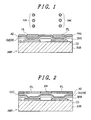
- FIG. 1 is a cross-sectional view showing an embodiment 1 of the present invention.
- a substrate AMP in FIG. 1 is an active matrix substrate (or a thin film transistor substrate or a TFT substrate in an abbreviated form) which constitutes an organic EL display device.
- a cathode CD which constitutes a first electrode, is formed for every pixel on a main face of an insulating substrate (here, a glass substrate) SUB.
- the cathode CD is formed by the patterning of a conductive metal film.
- the conductive metal film an alloy of aluminum and lithium fluoride (LiF) is used.
- a Mg/Al alloy, Mg/in alloy and the like can be used.
- Such a conductive metal film is formed on a main face of the glass substrate SUB by vapor deposition, sputtering, CVD or the like, and a desired patterning is performed through a photolithography step or the like, thus forming a cathode CD for every pixel. It is preferable that the cathode CD has a favorable reflectance.
- an insulation film (hereinafter referred to as “an interlayer film”) which covers the cathodes CD is formed.
- the interlayer film may be formed of an inorganic material, such as silicon nitride (SiN), on the main face of the substrate SUB, including the cathodes CD, using a chemical vapor deposition method. Further, the interlayer film may be formed by applying an organic material, such as Novorak resin or the like, to the main face of the substrate SUB by coating and curing the Novorak resin thereafter. The interlayer film is subjected to patterning such that upper surfaces of the cathodes CD are exposed, thus forming partition banks (also referred to as “banks”) BNK. A region which includes an upper surface of the cathode CD, which is surrounded by the banks BNK, corresponds to one pixel (a sub pixel for color display).
- An organic EL light emitting layer (also referred to as “an organic EL layer”) OLE is formed above the banks BNK and the cathodes CD to cover the banks BNK and the cathodes CD.
- the organic EL light emitting layer OLE is formed typically by a mask vapor deposition method, it is possible to use other methods, such as an ink jet method or patterning using a photolithography method after forming a thin film, depending on the material of the organic light emitting layer OLE.
- an electron transport layer (Alq) a first organic light emitting layer, a second organic light emitting layer, and a hole transport layer ( ⁇ -NPD) are stacked sequentially.
- BH-120 In forming the first organic light emitting layer, BH-120, a product of ldemitsu Kosan Co., Ltd., is used as a host material, and RD-001X, a product of Idemitsu Kosan Co., Ltd, is used as a dopant.
- BH-120 In forming the second organic light emitting layer, BH-120, a product of ldemitsu Kosan Co., Ltd., is used as a host material, and BD-102, a product of ldemitsu Kosan Co., Ltd, is used as a dopant.
- the organic light emitting layer OLE(W) which is capable of emitting a white light, is obtained using both the first light emitting layer and the second light emitting layer.
- An ITO film is formed to cover a front surface of the organic EL light emitting layer OLE(W), thus forming a transparent anode AD, which constitutes a second electrode.
- the transparent anode AD is not limited to an ITO film, and it may be formed of another transparent conductive film, such as a transparent metal film.
- a protective layer PAS is formed over the transparent anode AD.
- the organic EL light emitting layer OLE(W), the transparent anode AD and the protective layer PAS define surface shapes (recessed portions) which trace the shapes of the banks BNK.
- the protective layer PAS is formed for protecting the organic EL light emitting layer OLE(W) and for controlling the wettability in forming the color filters using an ink jet method in a succeeding step.
- the protective layer PAS also prevents deterioration of the properties of the organic EL light emitting layer OLE(W) by the color filter material (ink) applied using the ink jet method.
- the protective layer PAS is formed using a plasma CVD. When it is necessary to ensure the wettability, an ultra-violet-ray (UV) irradiation is performed optionally. It is also possible to adopt a film forming method in which a metal alkoxide is formed into a film by spin coating and is baked thereafter. Here, depending on the process condition, the formation of the protective layer PAS may be omitted.
- color filters FIL having three colors R, G, B
- FIG. 1 the coating of only color filters of two colors is shown. Although it is desirable to form the color filters FIL having three colors simultaneously from the point of view of shortening the manufacturing steps, this is not a requisite.
- the banks BNK suppress the mixing of the color-filter-material inks INK dropped from the nozzle.
- the color filters FIL are covered with a sealing member, such as a glass plate, a resilient film or the like, having a light transmitting property, thus sealing the surrounding area of the color filters FIL so as to prevent deterioration of the operational properties attributed to invasion of moisture from the surrounding environment, whereby a stable display is realized.
- a sealing member such as a glass plate, a resilient film or the like, having a light transmitting property
- the embodiment 1 adopts a top anode constitution in which the first electrode and the second electrode are respectively formed of the cathode CD and the transparent anode AD, by selecting the electrode material, the organic light emitting material, the process condition and the like, the embodiment 1 can adopt a top cathode constitution in which the first electrode is formed of the anode and the second electrode is formed of the cathode.
- the color filters which form the respective pixels can be directly formed on the substrate on which the white-light organic light emitting layer is formed using the ink jet method, and, therefore, it is possible to provide an organic EL display device capable of high definition, which is free from displacement or shifting of the three colors.
- FIG. 2 is a cross-sectional view showing an embodiment 2 of the present invention.
- the illustration of the color-filter-material ink INK indicated in FIG. 1 is omitted in FIG. 2 for purposes of simplification of the drawing.
- the TFT substrate AMP of the embodiment 2 is substantially the same as that of embodiment 1 until the step in which the cathodes CD, which constitute the first electrodes, the banks BNK, the organic light emitting layer OLE(W) and the transparent anode AD, which constitutes the second electrode, are formed in this order on the upper surface of the glass substrate SUB.
- the organic material is applied to the upper surface of the transparent anode AD so as to form an interlayer film OVC which covers the transparent anode AD, whereby the undulation of an upper surface of the transparent anode AD (in other words, an irradiation surface of light from the organic light emitting layer OLE(W)) which is generated by the banks (BNK) or the like can be leveled. Accordingly, the surface of the transparent anode AD is eliminated.
- the interlayer film OVC is made of a material which belongs to a metal alkoxide group.
- the interlayer film OVC made of metal alkoxide is applied, with a film thickness (desirably 1 ⁇ m or more) equal to or more than a degree which can level the upper surface of the transparent anode AD, by spin coating, the UV irradiation is performed under a mixed atmosphere of ozone and nitrogen so as to enhance the oxidizing property, and the interlayer film OVC is cured at a low temperature (desirably, 100° C. or less).
- a light blocking layer (black matrix) BM is formed between the pixels, that is, right above the banks BNK by screen printing using a mask. Further, the color-filter-material ink INK is dropped into the openings of the black matrix BM from the nozzle of the ink jet device so as to form the color filters FIL.
- the step in which the interlayer film OVC made of metal alkoxide is treated under a mixed atmosphere of ozone and nitrogen is an option which is adopted to shorten the treatment time, and, hence, the step is not a requisite.
- the color filters FIL are covered with a sealing member, such as a glass plate, a flexible film or the like, having light transmitting property, thus sealing the surrounding area of the color filters FIL so as to prevent deterioration of the operational properties attributed to invasion of moisture from the surrounding environment, whereby a stable display is realized.
- a sealing member such as a glass plate, a flexible film or the like, having light transmitting property
- the flatness of the organic EL light emitting layer can be made uniform between the pixels, and, at the same time, a leaking of light from a neighboring pixel can be prevented by properly selecting the refractive index of the interlayer film OVC and the size of opening portions of the pixels formed by the black matrix BM, whereby it is possible to obtain an image display of high contrast and high color purity.
- the embodiment 2 can also adopt a top cathode constitution in the same manner as the embodiment 1.
- FIG. 3 is a cross-sectional view showing an embodiment 3 of the present invention.
- the illustration of the color-filter-material ink INK shown in FIG. 1 is omitted.
- the TFT substrate AMP of the embodiment 3 is substantially the same as the TFT substrate AMP of the embodiment 1 and the embodiment 2 up to the formation of the cathodes CD, which constitute the first electrodes, and the banks BNK formed on the main face of the glass substrate SUB.
- an organic light emitting layer OLE (B), which emits blue light is formed in a state such that the organic light emitting layer OLE (B) covers the banks BNK and the opening portions of the cathodes CD.
- the height of the banks BNK in the embodiment 3 is set to be larger than the height of the banks BNK in the embodiment 1 and the embodiment 2.
- the anode AD which constitutes the second electrode, is formed in a state such that the anode AD covers the whole surface of the organic light emitting layer OLE (B), and then a first protective layer PAS 1 is formed above the anode AD.
- ink material for forming wavelength converting filters (a color changing medium which converts the blue light into three respective colors) is dropped from the nozzle of the ink jet device into the recessed portions formed by the banks BNK, thus forming wavelength converting filters CCF of three colors (R, G, B).
- FIG. 3 only the coating of the wavelength converting filters of two colors is shown.
- the banks BNK suppress the mixing of the wavelength-converting-filter-material ink dropped from the nozzle.
- the pixel for the color blue (B) may adopt a constitution in which the wavelength converting filter is not applied.
- a second protective layer PAS 2 which also functions as an interlayer film, is formed as a film in a state such that the second protective layer PAS 2 covers the wavelength converting filter CCF.
- the second protective layer PAS 2 is also made of silicon nitride (SiN) or silicon oxide (SiO) in the same manner as the first protective layer PAS 1
- the second protective layer PAS 2 may be formed using other similar materials, such as an amorphous carbon film, for example, by a plasma CVD method or sputtering.
- the carbon film which is formed by the plasma CVD method constitutes a diamond-like hard film.
- color-filter-material ink is dropped into recessed portions of the second protective layer PAS 2 , which follow the surface shape of the banks BNK, from the nozzle of the ink jet device, thus forming color filters FIL of three colors (R, G, B).
- FIG. 3 shows only the coating of the color filters of two colors.
- the banks BNK suppress the mixing of color-filter-material inks dropped from the nozzle.
- the pixel for the color blue (B) may have a constitution in which the color filter is not applied.
- the upper surfaces of the color filters FIL are covered with a sealing member, such as a glass plate, a flexible film or the like, having a light transmitting property, thus sealing the surrounding area of the color filters FIL, so as to prevent deterioration of the operational properties attributed to the invasion of moisture from the surrounding environment, whereby a stable display is realized.
- a sealing member such as a glass plate, a flexible film or the like, having a light transmitting property
- the embodiment 3 with the use of the organic light emitting layer OLE (B), which emits a blue light that exhibits a higher luminance and has a longer lifetime than the currently available organic light emitting layer OLE (W), which is capable of emitting the white light, it is possible to obtain an image display of high luminance and high contrast.
- the embodiment 3 also can adopt a top cathode constitution in the same manner as the embodiment 1 and the embodiment 2.
- FIG. 4 is a diagrammatic cross-sectional view showing one example of a sealing member which seals a color filter forming surface of the TFT substrate AMP, which constitutes the organic BL display device of the present invention.
- the sealing member CVP provides an absorbent (desiccant) layer DES on an inner surface of a glass plate SLS.
- FIG. 5 is a schematic circuit diagram showing a constitutional example of a pixel of the organic EL display device.
- the pixel PX constitutes a sub pixel in the color display.
- the pixel PX is constituted of a thin film transistor TFT 1 for switching, which is connected to a scanning line GL and a data line DL, a storage capacitance CPR, which stores display data supplied from the data line DL as a charge when the thin film transistor TFT is selected by the scanning line GL, a thin film transistor TFT 2 which drives an organic EL element OLE, and a current supply line CSL.
- the thin film transistor TFT 1 has the gate electrode thereof connected to the scanning line GL and the drain electrode thereof connected to the data line DL. Further, the gate electrode of the thin film transistor TFT 2 is connected to the source electrode of the thin film transistor TFT 1 , and one electrode (+pole) of the storage capacitance CPR is connected to this node.
- the thin film transistor TFT 2 has the drain electrode thereof connected to the current supply line CSL and the source electrode thereof connected to the anode AD of the organic EL element OLE.
- the display data supplied from the data line DL is stored in the storage capacitance CPR. Further, at a point of time when the thin film transistor TFT 1 is turned off, the thin film transistor TFT 2 is turned on and an electric current flows from the current supply line CSL to the organic EL element OLE, and the current is held for a period of substantially 1 frame (or 1 field).
- the electric current which flows here is defined by a charge corresponding to the data signal stored in the storage capacitance CPR.
- the circuit shown in FIG. 5 has the simplest constitution, and other various circuit constitutions can be used.
- FIG. 6 is a plan view of the vicinity of a pixel showing a structural example of the circuit of the pixel shown in FIG. 5 on a substrate.
- the same symbols used in FIG. 5 correspond to identical portions, wherein symbol DE indicates the opening portion of the pixel.
- the thin film transistor TFT 1 and the thin film transistor TFT 2 are arranged on a non-display portion, which is arranged close to the opening portion DE of the pixel.
- FIG. 7 is an equivalent circuit diagram including a drive circuit of the organic EL display device.
- the pixels PX are arranged in a matrix array to form a display region AR.
- the data lines DL are driven by a data line drive circuit DDR.
- the scanning lines GL are driven by a scanning line drive circuit GDR.
- the current supply line CSL is connected to a current supply circuit (not shown in the drawing) through a current supply bus line CSLB.
- symbol TM indicates external input terminals.
- FIG. 8 is an equivalent circuit diagram which shows the constitution of an organic EL display device that is capable of producing a full color display.
- the respective display portions R, G, B of three colors are constituted of pixels (sub pixels) PX shown in FIG. 7 , and they are arranged in the direction of the scanning line GL to form one color pixel (constituted of the respective sub pixels PX of R, G, B).
- Other constitutions of this equivalent circuit are substantially the same as the corresponding constitutions shown in FIG. 7 .
- the advantageous effect in which the mixing of colors to the neighboring pixel can be prevented by realizing a coating of the materials of different color filters or the different wavelength converting filters with high accuracy using an ink jet device, is not limited to an organic EL display device. That is, it is possible to obtain substantially the same advantageous effect by applying such a technical concept to other display devices, for example, a display device which uses plasma elements.
Abstract
Description
Claims (16)
Applications Claiming Priority (2)
| Application Number | Priority Date | Filing Date | Title |
|---|---|---|---|
| JP2004-206105 | 2004-07-13 | ||
| JP2004206105A JP2006032010A (en) | 2004-07-13 | 2004-07-13 | Organic el display device |
Publications (2)
| Publication Number | Publication Date |
|---|---|
| US20060012288A1 US20060012288A1 (en) | 2006-01-19 |
| US7893607B2 true US7893607B2 (en) | 2011-02-22 |
Family
ID=35598750
Family Applications (1)
| Application Number | Title | Priority Date | Filing Date |
|---|---|---|---|
| US11/178,421 Active 2027-03-05 US7893607B2 (en) | 2004-07-13 | 2005-07-12 | Organic electroluminescence display device |
Country Status (3)
| Country | Link |
|---|---|
| US (1) | US7893607B2 (en) |
| JP (1) | JP2006032010A (en) |
| CN (1) | CN1722925A (en) |
Cited By (4)
| Publication number | Priority date | Publication date | Assignee | Title |
|---|---|---|---|---|
| US20130099221A1 (en) * | 2010-08-06 | 2013-04-25 | Panasonic Corporation | Organic el display panel, and method for producing same |
| US20150048333A1 (en) * | 2013-08-13 | 2015-02-19 | Samsung Display Co., Ltd. | Organic light emitting diode display and method for preparing the same |
| US9513523B2 (en) * | 2014-12-31 | 2016-12-06 | Hon Hai Precision Industry Co., Ltd. | Thin film transistor array substrate and method of fabricating same |
| US10825871B2 (en) | 2015-12-28 | 2020-11-03 | Samsung Display Co., Ltd. | Organic light-emitting display apparatus and method of manufacturing the same |
Families Citing this family (40)
| Publication number | Priority date | Publication date | Assignee | Title |
|---|---|---|---|---|
| JP2007234391A (en) * | 2006-03-01 | 2007-09-13 | Seiko Epson Corp | Electroluminescence display device and electronic apparatus |
| JP2008066216A (en) * | 2006-09-11 | 2008-03-21 | Seiko Epson Corp | Organic electroluminescence device, its manufacturing method and electronic apparatus |
| JP2008277270A (en) * | 2007-03-30 | 2008-11-13 | Dainippon Printing Co Ltd | Light-emitting organic el display panel |
| JP2009020493A (en) * | 2007-06-13 | 2009-01-29 | Canon Inc | Organic el panel |
| KR101391326B1 (en) | 2007-09-19 | 2014-05-07 | 샤프 가부시키가이샤 | Color conversion filter, and process for producing color conversion filter and organic el display |
| JP5214360B2 (en) | 2008-07-29 | 2013-06-19 | シャープ株式会社 | Color conversion organic EL display |
| WO2010092688A1 (en) | 2009-02-16 | 2010-08-19 | 富士電機ホールディングス株式会社 | Process for producing color conversion filter |
| TWI491303B (en) * | 2009-06-29 | 2015-07-01 | 群創光電股份有限公司 | Image display system |
| JP5452178B2 (en) * | 2009-11-12 | 2014-03-26 | 株式会社日立ハイテクノロジーズ | Vacuum deposition apparatus, vacuum deposition method, and organic EL display device manufacturing method |
| WO2011061789A1 (en) | 2009-11-17 | 2011-05-26 | 富士電機ホールディングス株式会社 | Organic el display |
| JP5601025B2 (en) | 2010-05-21 | 2014-10-08 | セイコーエプソン株式会社 | Electro-optical device, method of manufacturing electro-optical device, and electronic apparatus |
| JP5605050B2 (en) * | 2010-07-21 | 2014-10-15 | セイコーエプソン株式会社 | Manufacturing method of organic EL device |
| KR101784994B1 (en) * | 2011-03-31 | 2017-10-13 | 삼성디스플레이 주식회사 | Organic light emitting diode display and manufacturing method thereof |
| FR2973941B1 (en) * | 2011-04-11 | 2013-05-03 | Commissariat Energie Atomique | ORGANIC OPTOELECTRONIC DEVICE AND METHOD OF ENCAPSULATION |
| KR101980233B1 (en) * | 2012-09-04 | 2019-05-21 | 삼성디스플레이 주식회사 | Organic light emitting display apparatus and method of manufacturing thereof |
| CN103797531A (en) * | 2012-09-10 | 2014-05-14 | 深圳市柔宇科技有限公司 | Large-size display screen and manufacturing method therefor |
| JP5956918B2 (en) * | 2012-12-07 | 2016-07-27 | 株式会社ジャパンディスプレイ | Organic EL display device |
| US9024336B2 (en) * | 2013-05-28 | 2015-05-05 | J Touch Corporation | Display panel driven by electrode wires |
| KR20150010232A (en) * | 2013-07-18 | 2015-01-28 | 삼성디스플레이 주식회사 | Organic light emitting display apparatus and method of manufacturing the same |
| JP6247855B2 (en) * | 2013-07-26 | 2017-12-13 | 株式会社ジャパンディスプレイ | Light emitting element display device |
| TWI681559B (en) | 2013-10-10 | 2020-01-01 | 日商精工愛普生股份有限公司 | Light-emitting device and electronic apparatus having the same |
| JP6284346B2 (en) * | 2013-11-25 | 2018-02-28 | 株式会社ジャパンディスプレイ | Organic EL display device |
| JP2015128003A (en) | 2013-12-27 | 2015-07-09 | ソニー株式会社 | Display device and electronic apparatus |
| JP5937124B2 (en) * | 2014-03-10 | 2016-06-22 | ユニファイド イノヴェイティヴ テクノロジー, エルエルシー | Organic EL display |
| JP6528370B2 (en) | 2014-07-25 | 2019-06-12 | セイコーエプソン株式会社 | Light emitting device and electronic device |
| WO2016098954A1 (en) * | 2014-12-18 | 2016-06-23 | 엘지전자 주식회사 | Organic light-emitting diode display device |
| JP2015156381A (en) * | 2015-03-31 | 2015-08-27 | ユニファイド イノヴェイティヴ テクノロジー, エルエルシー | Organic electroluminescence (el) display |
| KR102609507B1 (en) * | 2015-12-30 | 2023-12-04 | 엘지디스플레이 주식회사 | White light emitting device and hybrid display device using the same |
| CN111627924B (en) * | 2016-06-14 | 2023-05-16 | 群创光电股份有限公司 | Display device and method for manufacturing display device |
| KR101965157B1 (en) * | 2017-02-28 | 2019-04-08 | 한국생산기술연구원 | Quantum dot hybrid organic light emitting display device and method for manufacturing the same |
| KR20190033979A (en) * | 2017-09-22 | 2019-04-01 | 주식회사 루멘스 | vertical type light emitting elements having color conversion electrode part |
| US10693104B2 (en) * | 2017-12-26 | 2020-06-23 | Sakai Display Products Corporation | Organic electroluminescent device and method for producing same |
| WO2019150506A1 (en) * | 2018-01-31 | 2019-08-08 | 堺ディスプレイプロダクト株式会社 | Organic el display device and manufacturing method thereof |
| JP6442117B1 (en) * | 2018-01-31 | 2018-12-19 | 堺ディスプレイプロダクト株式会社 | Manufacturing method of organic EL display device |
| CN110164910B (en) * | 2018-05-28 | 2021-04-23 | 京东方科技集团股份有限公司 | Color conversion layer, preparation method thereof and display device |
| KR20200054423A (en) * | 2018-11-09 | 2020-05-20 | 삼성디스플레이 주식회사 | Display device and method of manufacturing of the same |
| KR20210042195A (en) * | 2019-10-08 | 2021-04-19 | 삼성디스플레이 주식회사 | Display device |
| KR20210043776A (en) * | 2019-10-11 | 2021-04-22 | 삼성디스플레이 주식회사 | Color-converting substrate, display device including the same and method for manufacturing the same |
| KR20210118292A (en) * | 2020-03-19 | 2021-09-30 | 삼성디스플레이 주식회사 | Display apparatus |
| KR20220021978A (en) * | 2020-08-14 | 2022-02-23 | 삼성디스플레이 주식회사 | Display device |
Citations (7)
| Publication number | Priority date | Publication date | Assignee | Title |
|---|---|---|---|---|
| US5932327A (en) * | 1995-02-09 | 1999-08-03 | Nippondenso Co., Ltd. | Electroluminescent element |
| US6140766A (en) * | 1997-12-27 | 2000-10-31 | Hokuriku Electric Industry Co., Ltd. | Organic EL device |
| US20020093284A1 (en) * | 2001-01-15 | 2002-07-18 | Masaya Adachi | Light-emitting devices and light-emitting displays |
| US20030107314A1 (en) * | 2001-12-06 | 2003-06-12 | Tetsuo Urabe | Display and method of manufacturing the same |
| US6624567B2 (en) * | 2000-06-08 | 2003-09-23 | Tohoku Pioneer Corporation | Organic electroluminescent display panel and its manufacturing method |
| US20040000864A1 (en) | 2002-06-27 | 2004-01-01 | Yoshifumi Kato | Color display unit |
| US20050146266A1 (en) | 2002-02-12 | 2005-07-07 | Hitoshi Kuma | Organic el display and its production method |
Family Cites Families (2)
| Publication number | Priority date | Publication date | Assignee | Title |
|---|---|---|---|---|
| JPH10162958A (en) * | 1996-11-28 | 1998-06-19 | Casio Comput Co Ltd | El element |
| JP3936170B2 (en) * | 2001-11-07 | 2007-06-27 | 双葉電子工業株式会社 | Top emission type organic EL element |
-
2004
- 2004-07-13 JP JP2004206105A patent/JP2006032010A/en active Pending
-
2005
- 2005-07-12 CN CNA2005100840166A patent/CN1722925A/en active Pending
- 2005-07-12 US US11/178,421 patent/US7893607B2/en active Active
Patent Citations (7)
| Publication number | Priority date | Publication date | Assignee | Title |
|---|---|---|---|---|
| US5932327A (en) * | 1995-02-09 | 1999-08-03 | Nippondenso Co., Ltd. | Electroluminescent element |
| US6140766A (en) * | 1997-12-27 | 2000-10-31 | Hokuriku Electric Industry Co., Ltd. | Organic EL device |
| US6624567B2 (en) * | 2000-06-08 | 2003-09-23 | Tohoku Pioneer Corporation | Organic electroluminescent display panel and its manufacturing method |
| US20020093284A1 (en) * | 2001-01-15 | 2002-07-18 | Masaya Adachi | Light-emitting devices and light-emitting displays |
| US20030107314A1 (en) * | 2001-12-06 | 2003-06-12 | Tetsuo Urabe | Display and method of manufacturing the same |
| US20050146266A1 (en) | 2002-02-12 | 2005-07-07 | Hitoshi Kuma | Organic el display and its production method |
| US20040000864A1 (en) | 2002-06-27 | 2004-01-01 | Yoshifumi Kato | Color display unit |
Cited By (8)
| Publication number | Priority date | Publication date | Assignee | Title |
|---|---|---|---|---|
| US20130099221A1 (en) * | 2010-08-06 | 2013-04-25 | Panasonic Corporation | Organic el display panel, and method for producing same |
| US8816339B2 (en) * | 2010-08-06 | 2014-08-26 | Panasonic Corporation | Organic EL display panel, and method for producing same |
| US20150048333A1 (en) * | 2013-08-13 | 2015-02-19 | Samsung Display Co., Ltd. | Organic light emitting diode display and method for preparing the same |
| US9513523B2 (en) * | 2014-12-31 | 2016-12-06 | Hon Hai Precision Industry Co., Ltd. | Thin film transistor array substrate and method of fabricating same |
| US10825871B2 (en) | 2015-12-28 | 2020-11-03 | Samsung Display Co., Ltd. | Organic light-emitting display apparatus and method of manufacturing the same |
| US10879317B2 (en) | 2015-12-28 | 2020-12-29 | Samsung Display Co., Ltd. | Organic light-emitting display apparatus and method of manufacturing the same |
| US11342388B2 (en) | 2015-12-28 | 2022-05-24 | Samsung Display Co., Ltd. | Organic light-emitting display apparatus comprising quantum dots |
| US11737336B2 (en) | 2015-12-28 | 2023-08-22 | Samsung Display Co., Ltd. | Organic light-emitting display apparatus comprising quantum dots |
Also Published As
| Publication number | Publication date |
|---|---|
| CN1722925A (en) | 2006-01-18 |
| US20060012288A1 (en) | 2006-01-19 |
| JP2006032010A (en) | 2006-02-02 |
Similar Documents
| Publication | Publication Date | Title |
|---|---|---|
| US7893607B2 (en) | Organic electroluminescence display device | |
| JP6479738B2 (en) | Non-common capping layer on organic devices | |
| KR100944311B1 (en) | Light emitting device and display device using the same | |
| KR101980233B1 (en) | Organic light emitting display apparatus and method of manufacturing thereof | |
| US8446091B2 (en) | Color conversion filter and manufacturing method of the organic EL display | |
| JP5808624B2 (en) | Display device and electronic device | |
| US7642109B2 (en) | Electrical connection in OLED devices | |
| US8957579B2 (en) | Low image sticking OLED display | |
| US20100277450A1 (en) | Display Device | |
| KR101903774B1 (en) | Organic light emitting diode display device and method for fabricating the same | |
| JP2006332019A (en) | Organic electroluminescent device and manufacturing method of organic electroluminescent device | |
| US20040140762A1 (en) | Organic EL device and method for producing the same | |
| KR20040036545A (en) | Electro-optical device and electronic apparatus | |
| US20090203285A1 (en) | Method for producing light-emitting device | |
| CN103681746A (en) | Organic light-emitting display apparatus and method of manufacturing the same | |
| JP2006073219A (en) | Display device and its manufacturing method | |
| CN103681745A (en) | Organic electroluminescent display and method of manufacturing the same | |
| JP2015002075A (en) | Light emitting element, display device and lighting system | |
| JP2011090925A (en) | Method for manufacturing electro-optical device | |
| US9698389B2 (en) | Method of producing organic EL device | |
| JP4678124B2 (en) | Electro-optical device, method of manufacturing electro-optical device, and electronic apparatus | |
| KR20110063227A (en) | Organic light emitting diode display device | |
| JP2011009093A (en) | Organic el device and electronic equipment | |
| JP2011054424A (en) | Top-emission type organic el display and method of manufacturing the same, and color filter used for it | |
| CN113299710A (en) | High resolution low power OLED display with extended lifetime |
Legal Events
| Date | Code | Title | Description |
|---|---|---|---|
| AS | Assignment |
Owner name: HITACHI DISPLAYS, LTD., JAPAN Free format text: ASSIGNMENT OF ASSIGNORS INTEREST;ASSIGNORS:TERAKADO, MASATOMO;KATO, SHINICHI;MATSUZAKI, EIJI;REEL/FRAME:016887/0897 Effective date: 20050809 |
|
| STCF | Information on status: patent grant |
Free format text: PATENTED CASE |
|
| AS | Assignment |
Owner name: IPS ALPHA SUPPORT CO., LTD., JAPAN Free format text: COMPANY SPLIT PLAN TRANSFERRING FIFTY (50) PERCENT SHARE OF PATENTS;ASSIGNOR:HITACHI DISPLAYS, LTD.;REEL/FRAME:027063/0019 Effective date: 20100630 Owner name: PANASONIC LIQUID CRYSTAL DISPLAY CO., LTD., JAPAN Free format text: MERGER;ASSIGNOR:IPS ALPHA SUPPORT CO., LTD.;REEL/FRAME:027063/0139 Effective date: 20101001 |
|
| FPAY | Fee payment |
Year of fee payment: 4 |
|
| MAFP | Maintenance fee payment |
Free format text: PAYMENT OF MAINTENANCE FEE, 8TH YEAR, LARGE ENTITY (ORIGINAL EVENT CODE: M1552); ENTITY STATUS OF PATENT OWNER: LARGE ENTITY Year of fee payment: 8 |
|
| AS | Assignment |
Owner name: SAMSUNG DISPLAY CO., LTD., KOREA, REPUBLIC OF Free format text: ASSIGNMENT OF ASSIGNORS INTEREST;ASSIGNORS:PANASONIC LIQUID CRYSTAL DISPLAY CO., LTD.;JAPAN DISPLAY INC.;SIGNING DATES FROM 20180731 TO 20180802;REEL/FRAME:046988/0801 |
|
| MAFP | Maintenance fee payment |
Free format text: PAYMENT OF MAINTENANCE FEE, 12TH YEAR, LARGE ENTITY (ORIGINAL EVENT CODE: M1553); ENTITY STATUS OF PATENT OWNER: LARGE ENTITY Year of fee payment: 12 |