US9513523B2 - Thin film transistor array substrate and method of fabricating same - Google Patents
Thin film transistor array substrate and method of fabricating same Download PDFInfo
- Publication number
- US9513523B2 US9513523B2 US14/812,151 US201514812151A US9513523B2 US 9513523 B2 US9513523 B2 US 9513523B2 US 201514812151 A US201514812151 A US 201514812151A US 9513523 B2 US9513523 B2 US 9513523B2
- Authority
- US
- United States
- Prior art keywords
- photoresist
- units
- color filter
- layer
- tft
- Prior art date
- Legal status (The legal status is an assumption and is not a legal conclusion. Google has not performed a legal analysis and makes no representation as to the accuracy of the status listed.)
- Active
Links
- 239000000758 substrate Substances 0.000 title claims abstract description 82
- 239000010409 thin film Substances 0.000 title claims abstract description 11
- 238000004519 manufacturing process Methods 0.000 title description 3
- 229920002120 photoresistant polymer Polymers 0.000 claims abstract description 111
- 125000006850 spacer group Chemical group 0.000 claims description 21
- 238000000034 method Methods 0.000 claims description 15
- 230000009849 deactivation Effects 0.000 claims description 4
- 238000000059 patterning Methods 0.000 claims description 4
- 239000004973 liquid crystal related substance Substances 0.000 description 9
- 239000000463 material Substances 0.000 description 9
- 239000011159 matrix material Substances 0.000 description 9
- 239000012780 transparent material Substances 0.000 description 6
- AMGQUBHHOARCQH-UHFFFAOYSA-N indium;oxotin Chemical compound [In].[Sn]=O AMGQUBHHOARCQH-UHFFFAOYSA-N 0.000 description 4
- -1 siloxanes Chemical class 0.000 description 4
- 239000000919 ceramic Substances 0.000 description 2
- 229920001971 elastomer Polymers 0.000 description 2
- 239000011521 glass Substances 0.000 description 2
- 238000012986 modification Methods 0.000 description 2
- 230000004048 modification Effects 0.000 description 2
- 239000004033 plastic Substances 0.000 description 2
- 229920003023 plastic Polymers 0.000 description 2
- 229920000515 polycarbonate Polymers 0.000 description 2
- 239000004417 polycarbonate Substances 0.000 description 2
- 229910021420 polycrystalline silicon Inorganic materials 0.000 description 2
- 229920000728 polyester Polymers 0.000 description 2
- 239000010453 quartz Substances 0.000 description 2
- VYPSYNLAJGMNEJ-UHFFFAOYSA-N silicon dioxide Inorganic materials O=[Si]=O VYPSYNLAJGMNEJ-UHFFFAOYSA-N 0.000 description 2
- XUIMIQQOPSSXEZ-UHFFFAOYSA-N Silicon Chemical compound [Si] XUIMIQQOPSSXEZ-UHFFFAOYSA-N 0.000 description 1
- 230000003247 decreasing effect Effects 0.000 description 1
- 229910010272 inorganic material Inorganic materials 0.000 description 1
- 239000011147 inorganic material Substances 0.000 description 1
- 239000011368 organic material Substances 0.000 description 1
- 229910052710 silicon Inorganic materials 0.000 description 1
- 239000010703 silicon Substances 0.000 description 1
Images


Classifications
-
- G—PHYSICS
- G02—OPTICS
- G02F—OPTICAL DEVICES OR ARRANGEMENTS FOR THE CONTROL OF LIGHT BY MODIFICATION OF THE OPTICAL PROPERTIES OF THE MEDIA OF THE ELEMENTS INVOLVED THEREIN; NON-LINEAR OPTICS; FREQUENCY-CHANGING OF LIGHT; OPTICAL LOGIC ELEMENTS; OPTICAL ANALOGUE/DIGITAL CONVERTERS
- G02F1/00—Devices or arrangements for the control of the intensity, colour, phase, polarisation or direction of light arriving from an independent light source, e.g. switching, gating or modulating; Non-linear optics
- G02F1/01—Devices or arrangements for the control of the intensity, colour, phase, polarisation or direction of light arriving from an independent light source, e.g. switching, gating or modulating; Non-linear optics for the control of the intensity, phase, polarisation or colour
- G02F1/13—Devices or arrangements for the control of the intensity, colour, phase, polarisation or direction of light arriving from an independent light source, e.g. switching, gating or modulating; Non-linear optics for the control of the intensity, phase, polarisation or colour based on liquid crystals, e.g. single liquid crystal display cells
- G02F1/133—Constructional arrangements; Operation of liquid crystal cells; Circuit arrangements
- G02F1/136—Liquid crystal cells structurally associated with a semi-conducting layer or substrate, e.g. cells forming part of an integrated circuit
- G02F1/1362—Active matrix addressed cells
- G02F1/1368—Active matrix addressed cells in which the switching element is a three-electrode device
-
- H—ELECTRICITY
- H01—ELECTRIC ELEMENTS
- H01L—SEMICONDUCTOR DEVICES NOT COVERED BY CLASS H10
- H01L27/00—Devices consisting of a plurality of semiconductor or other solid-state components formed in or on a common substrate
- H01L27/02—Devices consisting of a plurality of semiconductor or other solid-state components formed in or on a common substrate including semiconductor components specially adapted for rectifying, oscillating, amplifying or switching and having at least one potential-jump barrier or surface barrier; including integrated passive circuit elements with at least one potential-jump barrier or surface barrier
- H01L27/12—Devices consisting of a plurality of semiconductor or other solid-state components formed in or on a common substrate including semiconductor components specially adapted for rectifying, oscillating, amplifying or switching and having at least one potential-jump barrier or surface barrier; including integrated passive circuit elements with at least one potential-jump barrier or surface barrier the substrate being other than a semiconductor body, e.g. an insulating body
- H01L27/1214—Devices consisting of a plurality of semiconductor or other solid-state components formed in or on a common substrate including semiconductor components specially adapted for rectifying, oscillating, amplifying or switching and having at least one potential-jump barrier or surface barrier; including integrated passive circuit elements with at least one potential-jump barrier or surface barrier the substrate being other than a semiconductor body, e.g. an insulating body comprising a plurality of TFTs formed on a non-semiconducting substrate, e.g. driving circuits for AMLCDs
- H01L27/1259—Multistep manufacturing methods
-
- H—ELECTRICITY
- H01—ELECTRIC ELEMENTS
- H01L—SEMICONDUCTOR DEVICES NOT COVERED BY CLASS H10
- H01L29/00—Semiconductor devices adapted for rectifying, amplifying, oscillating or switching, or capacitors or resistors with at least one potential-jump barrier or surface barrier, e.g. PN junction depletion layer or carrier concentration layer; Details of semiconductor bodies or of electrodes thereof ; Multistep manufacturing processes therefor
- H01L29/66—Types of semiconductor device ; Multistep manufacturing processes therefor
- H01L29/68—Types of semiconductor device ; Multistep manufacturing processes therefor controllable by only the electric current supplied, or only the electric potential applied, to an electrode which does not carry the current to be rectified, amplified or switched
- H01L29/76—Unipolar devices, e.g. field effect transistors
- H01L29/772—Field effect transistors
- H01L29/78—Field effect transistors with field effect produced by an insulated gate
- H01L29/786—Thin film transistors, i.e. transistors with a channel being at least partly a thin film
- H01L29/78651—Silicon transistors
- H01L29/7866—Non-monocrystalline silicon transistors
- H01L29/78672—Polycrystalline or microcrystalline silicon transistor
-
- G—PHYSICS
- G02—OPTICS
- G02F—OPTICAL DEVICES OR ARRANGEMENTS FOR THE CONTROL OF LIGHT BY MODIFICATION OF THE OPTICAL PROPERTIES OF THE MEDIA OF THE ELEMENTS INVOLVED THEREIN; NON-LINEAR OPTICS; FREQUENCY-CHANGING OF LIGHT; OPTICAL LOGIC ELEMENTS; OPTICAL ANALOGUE/DIGITAL CONVERTERS
- G02F1/00—Devices or arrangements for the control of the intensity, colour, phase, polarisation or direction of light arriving from an independent light source, e.g. switching, gating or modulating; Non-linear optics
- G02F1/01—Devices or arrangements for the control of the intensity, colour, phase, polarisation or direction of light arriving from an independent light source, e.g. switching, gating or modulating; Non-linear optics for the control of the intensity, phase, polarisation or colour
- G02F1/13—Devices or arrangements for the control of the intensity, colour, phase, polarisation or direction of light arriving from an independent light source, e.g. switching, gating or modulating; Non-linear optics for the control of the intensity, phase, polarisation or colour based on liquid crystals, e.g. single liquid crystal display cells
- G02F1/133—Constructional arrangements; Operation of liquid crystal cells; Circuit arrangements
- G02F1/136—Liquid crystal cells structurally associated with a semi-conducting layer or substrate, e.g. cells forming part of an integrated circuit
- G02F1/1362—Active matrix addressed cells
- G02F1/136222—Colour filters incorporated in the active matrix substrate
-
- G02F2001/136222—
-
- H—ELECTRICITY
- H01—ELECTRIC ELEMENTS
- H01L—SEMICONDUCTOR DEVICES NOT COVERED BY CLASS H10
- H01L27/00—Devices consisting of a plurality of semiconductor or other solid-state components formed in or on a common substrate
- H01L27/02—Devices consisting of a plurality of semiconductor or other solid-state components formed in or on a common substrate including semiconductor components specially adapted for rectifying, oscillating, amplifying or switching and having at least one potential-jump barrier or surface barrier; including integrated passive circuit elements with at least one potential-jump barrier or surface barrier
- H01L27/12—Devices consisting of a plurality of semiconductor or other solid-state components formed in or on a common substrate including semiconductor components specially adapted for rectifying, oscillating, amplifying or switching and having at least one potential-jump barrier or surface barrier; including integrated passive circuit elements with at least one potential-jump barrier or surface barrier the substrate being other than a semiconductor body, e.g. an insulating body
- H01L27/1214—Devices consisting of a plurality of semiconductor or other solid-state components formed in or on a common substrate including semiconductor components specially adapted for rectifying, oscillating, amplifying or switching and having at least one potential-jump barrier or surface barrier; including integrated passive circuit elements with at least one potential-jump barrier or surface barrier the substrate being other than a semiconductor body, e.g. an insulating body comprising a plurality of TFTs formed on a non-semiconducting substrate, e.g. driving circuits for AMLCDs
- H01L27/1248—Devices consisting of a plurality of semiconductor or other solid-state components formed in or on a common substrate including semiconductor components specially adapted for rectifying, oscillating, amplifying or switching and having at least one potential-jump barrier or surface barrier; including integrated passive circuit elements with at least one potential-jump barrier or surface barrier the substrate being other than a semiconductor body, e.g. an insulating body comprising a plurality of TFTs formed on a non-semiconducting substrate, e.g. driving circuits for AMLCDs with a particular composition or shape of the interlayer dielectric specially adapted to the circuit arrangement
Definitions
- the subject matter herein generally relates to a thin transistor array substrate, and a method of fabricating a thin film transistor array substrate.
- Liquid crystal display includes a thin film transistor array substrate and a color filter substrate which are separately formed. An error of alignment can occur between the thin film transistor array substrate and the color filter substrate while assembling.
- FIG. 1 is a cross-sectional view of an embodiment of a first substrate with thin film transistors (TFTs).
- TFTs thin film transistors
- FIG. 2 is a cross-sectional view of an embodiment of a photoresist layer covering on the TFTs of FIG. 1 .
- FIG. 3 is a cross-sectional view of an embodiment of a plurality of spacers and a plurality of gaps formed via patterning the photoresist layer of FIG. 3 .
- FIG. 4 is a cross-sectional view of an embodiment of a red photoresist layer filling the gaps of FIG. 3 .
- FIG. 5 is a cross-sectional view of an embodiment of red photoresist units formed via patterning the red photoresist layer of FIG. 4 .
- FIG. 6 is a cross-sectional view of an embodiment of a green photoresist layer filling the rest gaps of FIG. 5 .
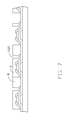
- FIG. 7 is a cross-sectional view of an embodiment of green photoresist units formed via patterning the green photoresist layer of FIG. 6 .
- FIG. 8 is a cross-sectional view of an embodiment of a blue photoresist layer covered the remainder of gaps of FIG. 7 .
- FIG. 9 is a cross-sectional view of an embodiment of a color filter layer formed by the red, the green, and the blue photoresist units of FIG. 8 .
- FIG. 10 is a cross-sectional view of an embodiment of a display panel of FIG. 1 .
- FIG. 11 is a cross-sectional view of a first embodiment of a display panel.
- FIG. 12 is a cross-sectional view of a second embodiment of a display panel.
- substantially is defined to be essentially conforming to the particular dimension, shape or other feature that the term modifies, such that the component need not be exact.
- substantially cylindrical means that the object resembles a cylinder, but can have one or more deviations from a true cylinder.
- comprising means “including, but not necessarily limited to”; it specifically indicates open-ended inclusion or membership in a so-described combination, group, series and the like.
- TFT thin film transistor
- FIGS. 1-9 illustrate an embodiment of a TFT array substrate 11 during fabrication.
- the TFT array substrate 11 includes a first substrate 110 and a plurality of TFTs 111 formed on the first substrate 110 .
- the TFTs 111 are spaced a first predetermined distance from each other.
- the TFT array substrate 11 further includes a photoresist layer 30 covering the first substrate 110 and the TFTs 111 .
- the photoresist layer 30 is cut to form a plurality of spacers 31 .
- the spacers 31 are spaced a second predetermined distance from each other to form a plurality of gaps 32 .
- the spacer 31 is located on an upper surface of a drain 1113 of a TFT 111 .
- the spacer 31 is substantially a trapezoidal shape.
- the photoresist layer 30 is a positive photoresist.
- the opening 1121 is substantially a trapezoidal shape.
- a width of the opening away from the first substrate 110 is wider than a width of the opening adjacent to the first substrate 110 .
- a width of the spacer 31 is in a range between 3-5 micrometer (mm)
- a height of the spacer 31 is in a range between 5-10 mm.
- the TFT array substrate 11 further includes a red photoresist layer 40 filling in the gap 32 .
- the red photoresist layer 40 is substantially coplanar with the TFT 111 .
- the red photoresist layer 30 is exposed and developed to form a plurality of red photoresist units R.
- the red photoresist units R are spaced a third distance from each other.
- Each of the red photoresist units R corresponds to an opening 1121 .
- the opening 1121 is formed by removing the spacer 31 disposed in a red photoresist unit R while exposing and developing the red photoresist layer 30 .
- the red photoresist layer 40 is a negative photoresist.
- Each of the adjacent red photoresist units R contains two TFTs 111 .
- the TFT array substrate 11 further includes a green photoresist layer 50 filling in the gaps 32 which are not filled with the red photoresist units R.
- the green photoresist layer 50 is substantially coplanar with the red photoresist units R.
- the green photoresist layer 50 is exposed and developed to form a plurality of green photoresist units G.
- the green photoresist units G are spaced the third distance from each other.
- Each of the green photoresist units G corresponds to an opening 1121 .
- the opening 1121 is formed by removing the spacer 31 disposed in the corresponding green photoresist unit G while exposing and developing the green photoresist layer 40 .
- the green photoresist layer 50 is a negative photoresist.
- Each of the green photoresist units G is adjacent to a red photoresist unit R.
- the TFT array substrate 11 further includes blue photoresist units B formed by filling blue photoresist in the gaps 32 which are not filled with the red photoresist units R or the green photoresist units G.
- the spacer 31 disposed in a blue photoresist unit B is removed to form an openings 1121 via an exposing and developing manner.
- Each of the blue photoresist units G is adjacent to a green photoresist unit G.
- the red photoresist units R, the green photoresist units G, and the blue photoresist units B are alternately disposed in the gaps 32 , and cooperate with each other to from a color filter layer 112 .
- the color filter layer 112 is also used as a deactivation layer of the TFT 111 .
- the TFT array substrate 11 further includes a plurality of white photoresist units W.
- the red photoresist units R, the green photoresist units G, the blue photoresist units B, and the white photoresist units W are orderly and alternately disposed in the gaps 32 , and cooperate with each other to from a color filter layer 112 .
- FIG. 10 illustrates an embodiment of the TFT array substrate 11 .
- the TFT array substrate 11 further includes a plurality of pixel electrodes 113 and an insulating layer 114 formed on the color filter layer 112 .
- the pixel electrode 113 is electrically connected with a drain of the TFT 111 via the openings 1121 .
- the pixel electrode layer 113 is sandwiched between the insulating layer 114 and the color filter layer 112 .
- the insulating layer 114 simultaneously covers the color filter layer 112 and the pixel electrodes 113 .
- the insulating layer 114 is made of silsesquioxane or siloxanes material.
- a thickness of the insulating layer 114 is in a range between 0.5-2.0 mm.
- the color filter 112 is directly formed on TFT array substrate 11 .
- the spacers 31 in a positive photoresist are formed on the TFT 111 , and are removed after forming the color filter 112 in a negative photoresist. Therefore, a size of the opening 1121 and the thickness of the TFT array substrate 11 can be decreased.
- FIG. 11 illustrates a first embodiment of a display panel 10 .
- the display panel 10 includes a TFT array substrate 11 , and an opposite substrate 12 , and a liquid crystal layer 23 sandwiched between the TFT array substrate 11 and the opposite substrate 12 .
- the TFT array substrate 11 includes a first substrate 110 , a plurality of TFTs 111 , a color filter layer 112 , a plurality of pixel electrodes 113 , and an insulating layer 114 .
- the first substrate 110 is made of transparent material, such as glass or quartz, or is made of inorganic, such as chip or ceramics, or is made of flexible organics, such as plastic, rubber, polyester, or polycarbonate.
- the TFT 111 is located on the first substrate 110 .
- the TFT 111 includes a gate 1110 , a gate insulating layer 1111 , a source 1112 , and a drain 1113 , and a path layer 1114 .
- the gate 1110 is located on the first substrate 110 .
- the gate insulating layer 1111 covers the gate 1110 and the first substrate 110 .
- the path layer 1114 is located above the gate insulating layer 1111 and corresponds to the gate 1110 .
- the source 1112 and the drain 1113 are symmetrically opposite on the gate insulating layer 1111 and the path layer 1114 .
- the TFT 111 is a low temperature poly-silicon thin film transistor.
- the color filter layer 112 covers the TFT 111 .
- the color filter layer 114 is considered as a deactivation layer of the TFT 111 .
- the color filter layer 112 includes a plurality of red photoresist units R, a plurality of green photoresist units G, and a plurality of blue photoresist units B.
- the red photoresist units R, the green photoresist units G, and the blue photoresist units B are alternately disposed on the TFT array substrate 11 .
- Each of the red photoresist units R, the green photoresist units G, and the blue photoresist units B defines an opening 1121 .
- a drain of the TFT 111 is exposed via the opening 1121 .
- a width of the opening 1121 is in a range between 3-5 micrometer (mm)
- a height of the spacer 31 is in a range between 5-10 mm.
- the opening 1121 is substantially a trapezoidal shape.
- a width of the opening 1121 away from the first substrate 110 is wider than a width of the opening 1121 adjacent to the first substrate 110 .
- the width of the opening 1121 from the first substrate 110 is 5 mm, and a width of the opening 1121 adjacent to the first substrate 110 is 3 mm.
- the pixel electrode 113 is located on an upper surface of the color layer 112 , and is electrically connected to the TFT 111 .
- the pixel electrode 113 is a made of transparent material, such as indium tin oxide.
- the pixel electrode 113 is capable of driving the liquid crystal layer 13 to rotate.
- the insulating layer 114 simultaneously covers the color filter layer 112 and the pixel electrodes 113 .
- the insulating layer 114 is made of made of silsesquioxane or siloxanes. silsesquioxane or siloxanes.
- a thickness of the insulating layer 114 is in a range between 0.5-2.0 mm.
- the opposite substrate 12 includes a second substrate 120 , a black matrix 121 , a flat layer 122 , and a common electrode layer 123 .
- the black matrix 121 cooperates with the color filter 112 to form a color filter of the display panel 10 .
- the black matrix 121 is located on a surface of the second substrate 120 adjacent to the liquid crystal layer 13 .
- the flat layer 122 is located on a surface of the black matrix 121 away from the second substrate 120 .
- the common electrode layer 123 is sandwiched between the second substrate 120 and the black matrix 121 . In at least one embodiment, the common electrode layer 123 cooperates with the pixel electrode 113 to drive the liquid crystal layer 130 to rotate.
- a material of the second substrate 120 is the same as the material of the first substrate 110 .
- the common electrode layer 123 is made of transparent material, such as indium tin oxide. In other embodiments, the material of the second substrate 120 is different from the material of the first substrate 110 .
- FIG. 12 illustrates a second embodiment of the display panel 20 .
- the display panel 20 includes a TFT array substrate 21 , and an opposite substrate 22 , and a liquid crystal layer 23 sandwiched between the TFT array substrate 21 and the opposite substrate 22 .
- the TFT array substrate 21 includes a first substrate 210 , a plurality of TFTs 211 , a color filter layer 212 , a plurality of pixel electrodes 213 , and an insulating layer 214 .
- the first substrate 210 is made of transparent material, such as glass or quartz, or is made of inorganic material, such as silicon chip or ceramics, or is made of flexible organic material, such as plastic, rubber, polyester, or polycarbonate.
- the TFT 211 is located on the first substrate 210 .
- the TFT 211 is a low temperature poly-silicon thin film transistor.
- the color filter layer 212 covers the TFT 211 .
- the color filter layer 214 is considered as a deactivation layer of the TFT 211 .
- the pixel electrode 213 is located on an upper surface of the color layer 212 , and is electrically connected to the TFT 211 .
- the pixel electrode 213 is made of transparent material, such as indium tin oxide.
- the pixel electrode 213 is capable of driving the liquid crystal layer 23 to rotate.
- the insulating layer 214 simultaneously covers the color filter layer 212 and the pixel electrodes 213 .
- the insulating layer 214 is made of made of silsesquioxane or siloxanes.
- a thickness of the insulating layer 114 is in a range between 0.5-2.0 mm.
- the display panel 20 further includes a black matrix 221 and a flat layer 222 .
- the black matrix 221 is located on the insulating layer 214 , and is opposite to a top surface of the TFT 211 .
- the black matrix 221 cooperates with the color filter layer 212 to form a color filter of the display panel 20 .
- the flat layer 222 covers the black matrix 221 and the insulating layer 214 .
- the opposite substrate 22 includes a second substrate 220 and a common electrode layer 223 .
- the common electrode layer 223 is located on a surface of the second substrate 220 adjacent to the liquid crystal layer 23 . In at least one embodiment, the common electrode layer 223 cooperates with the pixel electrode 213 to drive the liquid crystal layer 130 to rotate.
- a material of the second substrate 220 is equal to a material of the first substrate 210 .
- the common electrode layer 223 is made of transparent material, such as indium tin oxide. In other embodiments, the material of the second substrate 220 is different from the material of the first substrate 210 .
- the color filter layer is directly formed on TFT array substrate, and the opening are defined on the TFT via a positive photoresist and a negative photoresist. Therefore, a thickness of the display panel is reduced and the fabricating process for fabricating the display panel is simplified.
Abstract
Description
Claims (16)
Applications Claiming Priority (3)
| Application Number | Priority Date | Filing Date | Title |
|---|---|---|---|
| TW103146677A TWI557486B (en) | 2014-12-31 | 2014-12-31 | Thin film transistor substrate, method of manufacturing same and a display panel |
| TW103146677A | 2014-12-31 | ||
| TW103146677 | 2014-12-31 |
Publications (2)
| Publication Number | Publication Date |
|---|---|
| US20160187689A1 US20160187689A1 (en) | 2016-06-30 |
| US9513523B2 true US9513523B2 (en) | 2016-12-06 |
Family
ID=56163965
Family Applications (1)
| Application Number | Title | Priority Date | Filing Date |
|---|---|---|---|
| US14/812,151 Active US9513523B2 (en) | 2014-12-31 | 2015-07-29 | Thin film transistor array substrate and method of fabricating same |
Country Status (2)
| Country | Link |
|---|---|
| US (1) | US9513523B2 (en) |
| TW (1) | TWI557486B (en) |
Families Citing this family (4)
| Publication number | Priority date | Publication date | Assignee | Title |
|---|---|---|---|---|
| CN104965333B (en) * | 2015-07-15 | 2018-05-01 | 深圳市华星光电技术有限公司 | COA type liquid crystal display panels and preparation method thereof |
| KR102347665B1 (en) * | 2017-03-21 | 2022-01-07 | 삼성디스플레이 주식회사 | Display apparatus and method of manufacturing the same |
| US20190187527A1 (en) * | 2017-12-19 | 2019-06-20 | Shenzhen China Star Optoelectronics Semiconductor Display Technology Co., Ltd. | Array substrate, array substrate preparation method and display device |
| CN111696919B (en) * | 2020-07-23 | 2022-08-12 | 厦门天马微电子有限公司 | Array substrate, manufacturing method thereof and display device |
Citations (5)
| Publication number | Priority date | Publication date | Assignee | Title |
|---|---|---|---|---|
| US20040023425A1 (en) * | 2002-08-01 | 2004-02-05 | Industrial Technology Research Institute | Method of forming a color filter on a substrate having pixel driving elements |
| US20060093928A1 (en) * | 2004-11-03 | 2006-05-04 | Mu-Ching Hung | Manufacturing method of color filter on TFT array and manufacturing method of LCD panel |
| US20070247572A1 (en) * | 2006-04-21 | 2007-10-25 | Au Optronics Corp. | Transflective liquid crystal displays and methods for fabricating the same |
| US7893607B2 (en) * | 2004-07-13 | 2011-02-22 | Hitachi Displays., Ltd. | Organic electroluminescence display device |
| US20140104527A1 (en) * | 2012-10-17 | 2014-04-17 | Apple Inc. | Process Architecture for Color Filter Array in Active Matrix Liquid Crystal Display |
Family Cites Families (7)
| Publication number | Priority date | Publication date | Assignee | Title |
|---|---|---|---|---|
| CN100443930C (en) * | 2004-02-14 | 2008-12-17 | 鸿富锦精密工业(深圳)有限公司 | Color filter and display unit |
| TW200801820A (en) * | 2006-06-20 | 2008-01-01 | Sekisui Fine Chem Korea Co Ltd | Method for simultaneously forming color filter overcoat and column spacer of LCD and negative photoresist composition usable therein |
| TWI362506B (en) * | 2006-09-28 | 2012-04-21 | Au Optronics Corp | Method for fabricating color filters |
| TWI370271B (en) * | 2008-08-13 | 2012-08-11 | Chunghwa Picture Tubes Ltd | Color filter substrate and method of making the same |
| TW201044056A (en) * | 2009-06-03 | 2010-12-16 | Chi Mei Optoelectronics Corp | Color filter on array substrate and method for manufacturing the same and liquid crystal display panel and liquid crystal display device using the same |
| JP5741879B2 (en) * | 2013-01-25 | 2015-07-01 | 凸版印刷株式会社 | Color filter substrate and liquid crystal display device |
| JP6008891B2 (en) * | 2013-03-15 | 2016-10-19 | 富士フイルム株式会社 | Colored radiation-sensitive composition, colored cured film, color filter, colored pattern forming method, color filter manufacturing method, solid-state imaging device, and liquid crystal display device |
-
2014
- 2014-12-31 TW TW103146677A patent/TWI557486B/en active
-
2015
- 2015-07-29 US US14/812,151 patent/US9513523B2/en active Active
Patent Citations (5)
| Publication number | Priority date | Publication date | Assignee | Title |
|---|---|---|---|---|
| US20040023425A1 (en) * | 2002-08-01 | 2004-02-05 | Industrial Technology Research Institute | Method of forming a color filter on a substrate having pixel driving elements |
| US7893607B2 (en) * | 2004-07-13 | 2011-02-22 | Hitachi Displays., Ltd. | Organic electroluminescence display device |
| US20060093928A1 (en) * | 2004-11-03 | 2006-05-04 | Mu-Ching Hung | Manufacturing method of color filter on TFT array and manufacturing method of LCD panel |
| US20070247572A1 (en) * | 2006-04-21 | 2007-10-25 | Au Optronics Corp. | Transflective liquid crystal displays and methods for fabricating the same |
| US20140104527A1 (en) * | 2012-10-17 | 2014-04-17 | Apple Inc. | Process Architecture for Color Filter Array in Active Matrix Liquid Crystal Display |
Also Published As
| Publication number | Publication date |
|---|---|
| TW201624082A (en) | 2016-07-01 |
| US20160187689A1 (en) | 2016-06-30 |
| TWI557486B (en) | 2016-11-11 |
Similar Documents
| Publication | Publication Date | Title |
|---|---|---|
| US9711542B2 (en) | Method for fabricating display panel | |
| US9207494B2 (en) | Display device and method of manufacturing the same | |
| US9354478B2 (en) | Display substrate and method of manufacturing the same, and display device | |
| KR102007905B1 (en) | Display panel and liquid crystal display including the same | |
| US9287296B2 (en) | Display device | |
| US9482904B2 (en) | Liquid crystal display device and manufacturing method thereof | |
| US9791733B2 (en) | Array substrate, manufacture method thereof, and display device | |
| US9513523B2 (en) | Thin film transistor array substrate and method of fabricating same | |
| JP2007183632A (en) | Display panel and method of manufacturing the same | |
| JP2008309863A (en) | Method for manufacturing liquid crystal display panel, and liquid crystal display panel | |
| JP6220592B2 (en) | Liquid crystal display element and manufacturing method thereof | |
| US9595549B2 (en) | Display device comprising a plurality of microcavities and an encapsulation layer that seals the plurality of microcavities and method of manufacturing the same | |
| US10168570B2 (en) | Display apparatus | |
| US10067393B2 (en) | Thin film display panel and liquid crystal display device including the same | |
| US9411200B2 (en) | Liquid crystal display | |
| US20150116640A1 (en) | Liquid crystal component, method for fabricating the same, and liquid crystal display having the same | |
| US9664956B2 (en) | Liquid crystal display and manufacturing method thereof | |
| US20210356824A1 (en) | Coa array substrate and method of fabricating same | |
| US9383608B2 (en) | Array substrate and manufacturing method thereof | |
| US9810936B2 (en) | Display panel | |
| US9851595B2 (en) | Display device and manufacturing method thereof | |
| US20150378224A1 (en) | Display panel and method of manufacturing the same | |
| US20190129242A1 (en) | Display device | |
| US9477110B2 (en) | Display device and manufacturing method thereof | |
| JP2007017932A (en) | Display substrate, method of manufacturing the same, and display apparatus having the same |
Legal Events
| Date | Code | Title | Description |
|---|---|---|---|
| AS | Assignment |
Owner name: YE XIN TECHNOLOGY CONSULTING CO., LTD., TAIWAN Free format text: ASSIGNMENT OF ASSIGNORS INTEREST;ASSIGNORS:WU, MEI-LING;HOU, CHIH-YUAN;CHENG, HSIN-AN;AND OTHERS;SIGNING DATES FROM 20150520 TO 20150702;REEL/FRAME:036208/0460 |
|
| AS | Assignment |
Owner name: HON HAI PRECISION INDUSTRY CO., LTD., TAIWAN Free format text: ASSIGNMENT OF ASSIGNORS INTEREST;ASSIGNOR:YE XIN TECHNOLOGY CONSULTING CO., LTD.;REEL/FRAME:038930/0292 Effective date: 20160308 |
|
| STCF | Information on status: patent grant |
Free format text: PATENTED CASE |
|
| MAFP | Maintenance fee payment |
Free format text: PAYMENT OF MAINTENANCE FEE, 4TH YEAR, LARGE ENTITY (ORIGINAL EVENT CODE: M1551); ENTITY STATUS OF PATENT OWNER: LARGE ENTITY Year of fee payment: 4 |